
 Open Access Article
 This Open Access Article is licensed under a
 Creative Commons Attribution 3.0 Unported Licence
Electron/hole blocking layers as ionic blocking layers in perovskite solar cells
Sapir
Bitton
and
Nir
Tessler
 *
*
Microelectronics and Nanoelectronics Centers, Electrical Engineering Department, Technion Israel Institute of Technology, Haifa 32000, Israel. E-mail: nir@technion.ac.il
First published on 19th January 2021
Abstract
Theoretical studies of ion migration have thus far focused on migration within the perovskite layer only. This reflected a “hidden” assumption that the electron/hole blocking layers also function as ion blocking. Following experimental evidence, we study the effect of ion migration into the blocking layers and as a case study we compare our simulations to experimental results of device degradation under storage conditions (V = 0, dark), obtained by others. Good agreement is found between the simulated ion accumulation at the electrode interface with the experimental device degradation dynamics. Also, we find that the migration into the blocking layers dominates the effects on the device energy level diagram and that it may also turn the intrinsic perovskites into either p or n type solar cells. Although our simulations do not include the chemistry of degradation, they show two potential mechanisms associated with ion out-diffusion. First, the electron/hole balanced solar cell structure becomes imbalanced (should be reversible). Second, ions reaching the electrode may react with it (i.e. irreversible).
Introduction
Organic–inorganic perovskites of the type CH3NH3PbX3 (X = Cl, Br, I) have been around for a while1 including for light harvesting2 and have gained significant attention once they broke the 10% efficiency barrier in solid state solar cells.3 Since the 2012 reports,3–5 the field has expanded and advanced rapidly with current record efficiencies exceeding 25% within less than a decade.6 Besides the efficiency benchmarking there have also been advances in understanding the chemistry, physics, and device chemical-physics of these cells.7–27 We20,28 and others23,29–33 have addressed ion migration within the perovskite layer through device models and its relation to hysteresis, built-in potential, traps, etc. In the context of device stability there are several experimental reports highlighting the process of ion migration into the electron/hole blocking layers.18,19,34 Hence, while most simulation results, today, contain the “hidden” assumption that the electron/hole blocking layers also function as ion blocking, we will examine the effect of ion migration into the electron/hole blocking layers.35 This work was primarily inspired by Rivkin et al.19 who quantified the anion density within the hole blocking layer (HBL) and by Galatopoulos et al.18 which showed that the HBL may function as an ion blocking layer (IBL) too. Hence, while in ref. 35 we examined the ion migration under light and close to open circuit conditions, the current study is assuming dark and short-circuit conditions.Results
We study the ion migration within a perovskite solar cell of the form cathode/HBL/perovskite/EBL/anode (Fig. 1a), where EBL stands for the electron blocking layer. To simulate perfect electronic blocking, we assumed a 0.7eV blocking barrier between the perovskite and the BLs (Fig. 1b) and set the electron/hole mobility at a relatively high value. To ensure some relevance to the report by Galatopoulos et al.18 we study the ion migration under dark conditions, and the perovskite and blocking layers are 500 nm and 100 nm, respectively. Also, we set the ionic diffusion within the blocking layers to be 100 times slower compared to the perovskite layer. We note that 100 is an arbitrary number (≫1) and that the actual factor may be significantly higher, depending on the materials used for the electronic blocking layers or their polycrystalline nature. The modeling is carried out using a 2D model of the solar-cell implemented in Sentaurus TCAD and the physical properties used are listed in Table 1. Using the Sentaurus TCAD one can include rich physical picture including a range of recombination processes, including trap assisted ones, and sophisticated contact models. However, to keep the physical picture simple we implemented only bi-molecular recombination and Schottky type contacts. Regarding the dielectric constant, in the literature one may find values between 633 and 60.1 We chose 50 based on the temperature and frequency dependence measurements reported in ref. 1 and 36. Another issue to mention is that it is likely that the ionic motion induces secondary effects that impale the degradation either at the contacts,37,38 the blocking layers39 or in the bulk.40 Also, these degradation pathways are only part of those described in a recent review.41 All these potential degradation paths are not included in the simulation model and hence our model cannot directly predict cells’ degradation.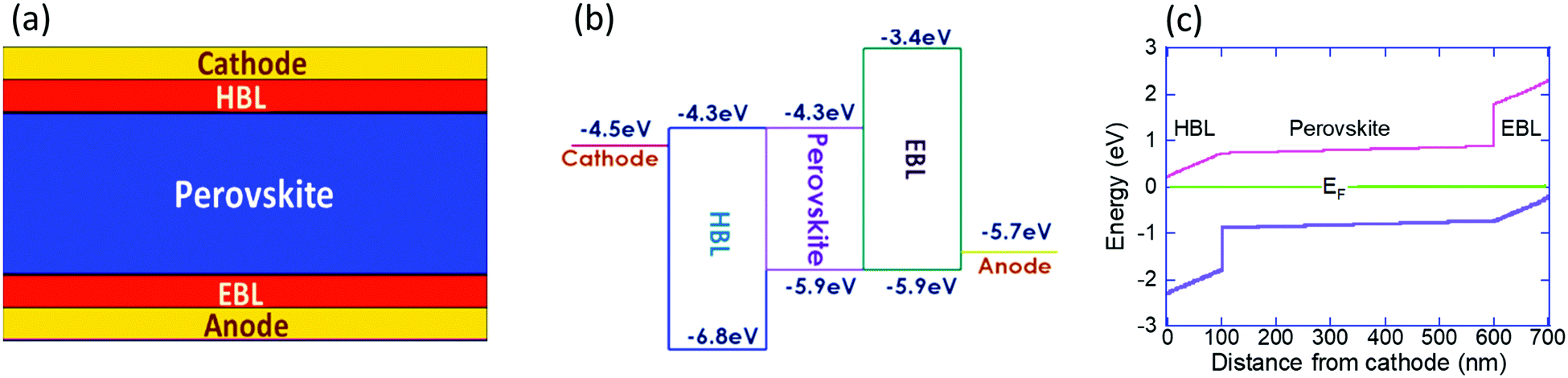 | ||
| Fig. 1 (a) Schematic description of the solar cell (b) energy levels used in the simulations. (c) Energy level diagram of the solar cell under short circuit and dark conditions calculated assuming none of the ions are mobile. | ||
| HBL | EBL | Perovskite | |
|---|---|---|---|
| Affinity, χ (eV) | 4.3 | 3.4 | 4.3 |
| Band gap, Eg (eV) | 2.5 | 2.5 | 1.6 |
| Charge mobility, μe = μh (cm2 V−1 s−1) | 10−2 | 10−2 | 2 |
| Dielectric constant, εr | 3 | 3 | 50 |
| Conduction density of states (cm−3) | 1021 | 1021 | 7 × 10¹⁸ |
| Valence density of states (cm−3) | 1021 | 1021 | 2.5 × 10¹⁸ |
| Initial free-ion density (cm−3) | 0 | 0 | 1018 |
| Cation diffusion, D (cm2 s−1) | 10−10 | 10−10 | 10−8 |
| Bimolecular recombination, B (cm2 s−1) | 1.2 × 10⁻⁸ | 1.2 × 10⁻⁸ | 10−10 |
| Contact injection barrier (eV) | 0.2 | 0.2 |
It is generally accepted that it is mostly one type of ion that migrates within the cell, but the exact identity may vary between reports or compositions.19,42–44 In our simulations we include only one type of mobile ion and it is the positive ion (cation) that is mobile. Namely, only singly charged cation is allowed to diffuse, and across the entire structure. However, by exchanging the roles of electrons and holes, the simulations also represent the case where only the anion is mobile. To assist such a conceptual exchange, we use an e/h symmetric device structure, in particular, when we discuss cation migration into the EBL which is equivalent to anion migration into the HBL. Namely, our results correspond well with I− migration into the PCBM layer.18,19Fig. 1c shows the energy level diagram of the solar cell under short circuit and dark conditions calculated assuming none of the ions are mobile. By saying that none of the ions are mobile we mean that anions (as I−) and cations (as MA+ and/or Pb+2) fully overlap and compensate each other. The values presented in Fig. 1c are relative to the Fermi level energy and we note that due to the high dielectric constant1,36,45 the voltage drop across the perovskite is negligible, and that the energy level diagram is fully symmetric.
Next, we use the calculation where all the ions are immobile, as the initial conditions for the time dependent simulation where the cations are allowed to drift-diffuse (dark and V = 0). In Fig. 2a–f we present the ions and electron/hole charge distribution. We compare the distributions at t = 0 (Fig. 2a and b) with those obtained at steady state (Fig. 2c–f). In Fig. 2c and d we present the results of our previous models (our Phase I) where we assumed the blocking layers to block also the ions. Fig. 2e and f show the steady state (t → ∞) distributions obtained by the current model (our Phase II). The left column describes the ions’ distributions where the light-green line is for the (immobile) anions and the fuchsia line describes the cation density distribution. Fig. 2a shows the initial free ion density (1018 cm−3) being uniformly distributed within the perovskite layer only. We chose 1018 cm−3 since our Phase I modeling indicated that for 1017 cm−3 to 1019 cm−3 the results are qualitatively similar and for 1016 cm−3 there was almost no effect of the ions. In Fig. 2c we see the known effect, where the combination of the built-in potential and the ion blocking by the BLs cause ion-accumulation at the perovskite–BL interface.20 Our Phase II results, Fig. 2e, are very different. The perovskite layer shows no ion accumulation but only depletion, on both sides. The mobile cations have separated from the immobile anions and have spilled primarily into the electron blocking layer (EBL) leaving the hole blocking layer (HBL) essentially empty. Note that the cations in the EBL have accumulated at the anode's interface, which in this simulation is blocking ions.
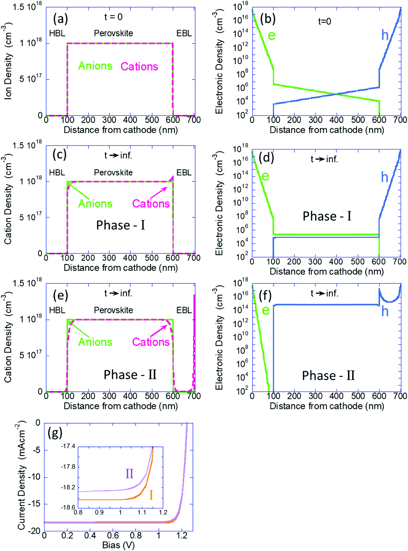 | ||
| Fig. 2 (a–f) Left column shows the ion density distribution and the right column the electronic charge distribution (a and b) are for t = 0, before any ion motion (c and d) are for our phase-I simulations where ions are blocked by the BLs (t → ∞) (e and f) are for our phase-II simulations where ions penetrate the BLs (t → ∞). (g) PCE curves of both models (see text for discussion). | ||
The right column of Fig. 2 describes the electron (green) and hole (blue) distributions. Fig. 2b shows the standard charge distribution expected of an intrinsic semiconductor under internal bias. Our Phase I results, Fig. 2d, indicate the effect of band flattening due to the ion migration within the perovskite layer. Our Phase II modeling where the ions are allowed to spill into the BLs shows an entirely different result (Fig. 2f). At this steady state (also equilibrium) the hole density inside the perovskite layer is orders of magnitude higher indicating that the ion spillage into the BLs has somewhat turned the perovskite layer from intrinsic to P-type semiconductor. An immediate question that may arise is wouldn’t this ion spillage destroy the device performance? In Fig. 2g we show the simulated PCE curves and we see that the ion-spillage created a negligible degradation. As discussed above, our simulations do not include any secondary effect of the ion motion such as trap formation or reaction with electrodes. Hence, while the real device would most certainly degrade, it won’t be due to the ion migration but due to the chemistry involved with such a motion (not included in our Phase II model).
To understand the p-type formation we need to examine the energy level diagram. To do so we follow a procedure similar to ref. 46 for studying the space charge, internal electric field, and the resulting band diagram modification. In Fig. 3 the left column is for t = 0 and the center and right columns are for t → ∞ as computed by our Phase I and Phase II models, respectively. Fig. 3a–c show the space charge within the perovskite solar cell devices. At t = 0 the only possible space charge is electronic and we note that the ohmic contacts induce a charge density of ∼5 × 1017 cm−3 at the contact interface. At steady state the cations have shifted in the perovskite layer (Fig. 3b) and in Fig. 3c they even spilled into the BLs with almost identical dipoles formed at the interfaces with the HBL and EBL. However, the most significant one is at the anode's interface with a density of 1.8 × 1018 cm−3.
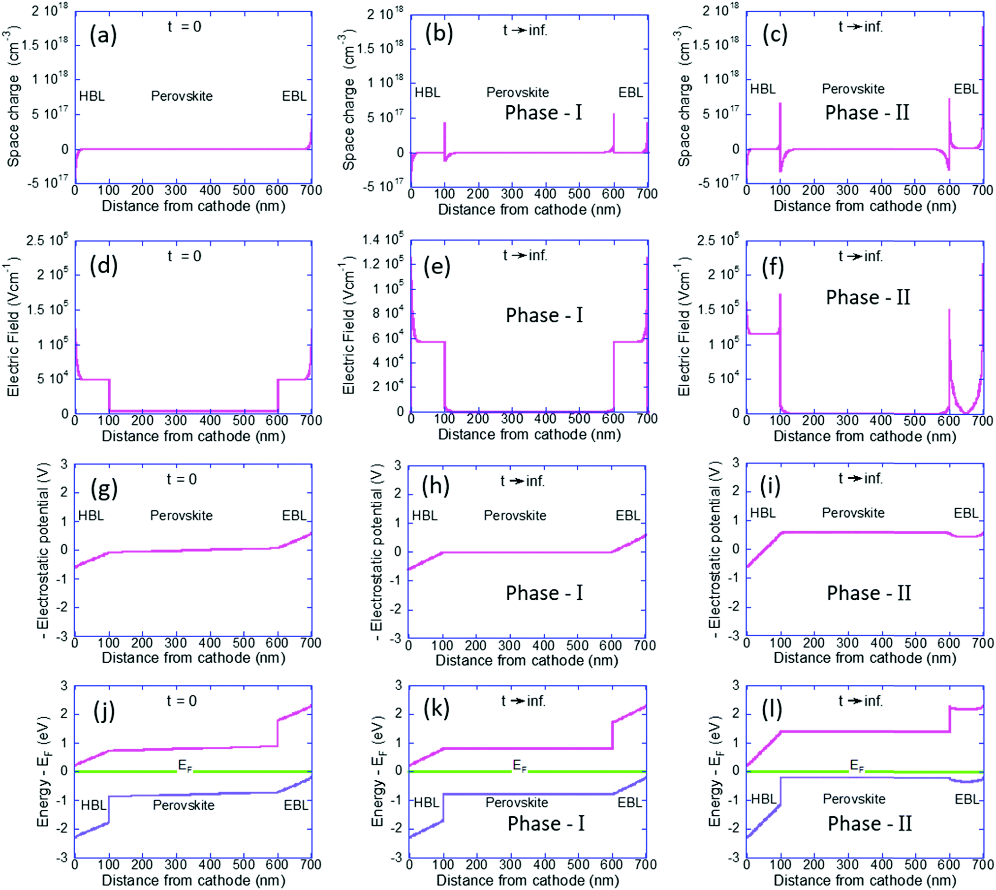 | ||
| Fig. 3 Left column is for t = 0, the center column is our phase-I simulations (t → ∞) where ions are blocked at the BLs, and the right column is our current, phase-II, simulations (t → ∞) (a–c) space charge distribution along the cell. (d–f) Internal electric field distribution. (g–i) The electrostatic potential times (−1) which represent the band modification induced by the internal electric field. (j–l) Energy level diagram relative to the Fermi level energy. | ||
Fig. 3d–f describe the internal electric field resulting from the space charge as well as the built-in potential. Fig. 3d is fully symmetric with the electric field at the BLs being slightly above 5 × 10⁴ V cm−1 and at the perovskite layer it is an order of magnitude lower at 3 × 10³ V cm−1. This difference in the electric field value reflects the difference in the dielectric constant (see Table 1). Fig. 3e is still symmetric and we note the effect of screening of the field at the perovskite layer. Fig. 3f is anything but symmetric. The dipoles at the interfaces with the BLs have reduced the electric field at the perovskite layer to zero. The dipole at the anode's interface screened most of the electric field in the EBL and as a result, the field drops primarily on the HBL.
Integrating over Fig. 3d–f will result in Fig. 3g–i, respectively 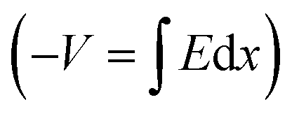 . In other words, Fig. 3g–i show the effect of the space charge on tilting the energy band diagram. Comparing these sub-figures, we note that the ions’ spillage into the EBL caused an upward shift of the levels which at the center of the device is from −0.015 eV to 0.58 eV, i.e. ∼0.6 eV shift. Also, the tilt that existed in the EBL (Fig. 3g and h) almost disappeared and was transferred to the HBL (Fig. 3i).
Lastly, Fig. 3j–l show the energy level diagram relative to the Fermi level energy. When the ions are forced to stay within the perovskite it remains intrinsic in nature however, the out diffusion of the cations turned the perovskite solar cell into a p-type one. This is in good agreement with Fig. 2f which shows only holes in the perovskite layer.
Using the fully symmetric structure we found that under storage conditions, the cations would spill out of the perovskite layer. This spillage modifies the nature of the perovskite layer (I to P) and creates cation accumulation at the anode. Using symmetry arguments, we may conclude that for the device studied by Galatopoulos et al.18 where the mobile ion was the anion I−, we would expect it to accumulate close to the cathode. Namely, diffusion through the PCBM is very likely to take place and it could be that indeed the thicker PCBM acted as the ion blocking layer, although the mechanism by which it blocked is not clear (yet).
Next, we move to examine the time evolution of the ion density at the contact interface. Galatopoulos et al.18 reported that enhancing the PCBM thickness resulted in a significantly longer device lifetime and attributed it to better ion blocking exhibited by thicker PCBM. To study this effect, we simulated several structures with varying BL thicknesses (25 nm, 50 nm, 100 nm, and 200 nm).
Fig. 4 shows the evolution of the ion density at the contact interface for different BL thicknesses, as depicted on the graph. The x axis is the simulation time, which for an ion diffusion coefficient of 10−10 cm2 s−1 translates into seconds and for ∼10−15 cm2 s−1 it translates into days. The top x-axis is an absolute reference as it is the distance the ions would have propagated due to diffusion only (i.e. the diffusion length at time “t” or  ). The inset shows the same data but with the x-axis being on log scale. The vertical dashed lines indicate the point where the ion density reached 90% of the steady state value. We note that the steady state density at the contact interface (Fig. 4) reduces as the contact is farther from the perovskite (i.e. thicker BL). This is somewhat similar to the effect found for the channel of a transistor47 with the opposite sign immobile-ions playing the role of the gate in pulling the cations back. The other effect we note is that for a short BL 90% density is reached for a diffusion length shorter than the BL's (12 nm < 25 nm) while for the longer it is reached for a diffusion length that is longer than the BL's length (340 nm > 200 nm). This is in line with the drift component being important close to t = 0 (Fig. 3j) or at short distances. At median times (medium distances) the bands at the EBL flatten and the ion transport becomes diffusion limited. At even longer times, not only the EBL bands flatten but a slight barrier to cation transport evolves at the perovskite/EBL interface (Fig. 3l). This small barrier is the manifestation of the immobile anions “pulling” (electrostatically) the cations back into the perovskite layer.
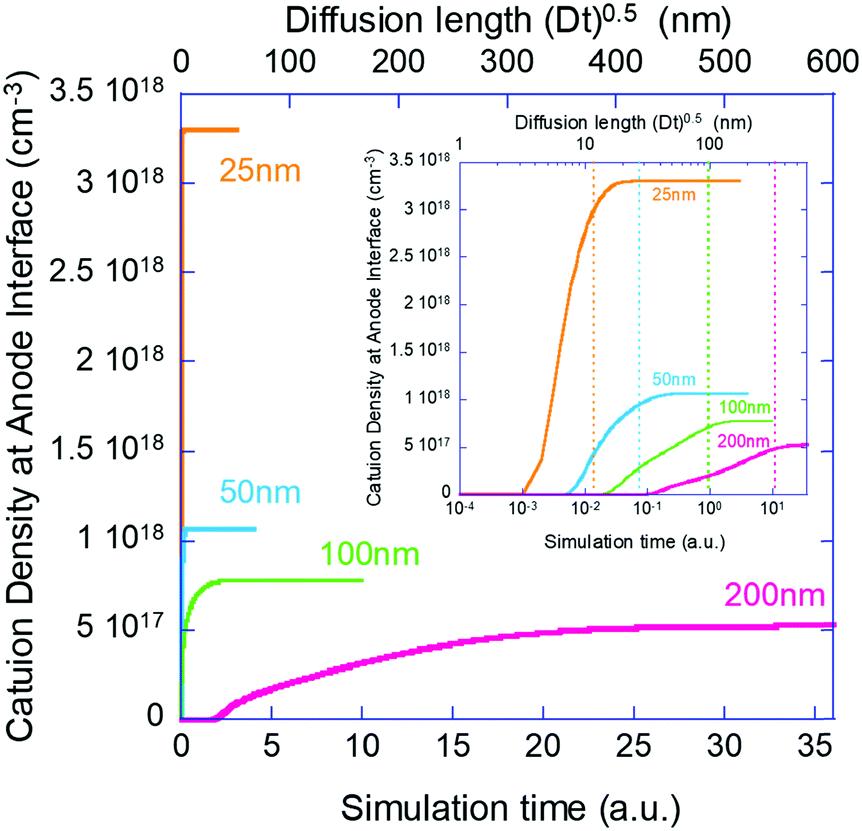 | ||
| Fig. 4 Ion density at the contact interface as a function of time and for different BL thicknesses, as depicted on the graph. The top x-axis shows the distance the ions could propagate through diffusion. Namely, it shows the ion diffusion length in the BLs. The inset presents the same data but with the x-axis being on log scale. The vertical dashed lines indicate the point where the ion density reached 90% of the steady state value. | ||
Discussion and conclusions
We have set to understand the ion diffusion into the electron/hole blocking layers (BLs) and the effect of the BLs being non-blocking for ions on the device characteristics. In Fig. 2 and 3 we compare the current model (our Phase II model) to results obtained from an older version of the model (our Phase I model). We note that the effect of ion motion within the perovskite layer only, is negligible compared to the one introduced by them spilling into the BLs. In a recent publication we showed that when operated close to the maximum power point the injection barrier at the contacts also plays a role.35 However, since we deal here with zero bias and zero light (zero current) the injection barriers were found to have no effect (not shown). To place the simulations on solid ground we chose to perform them under experimental conditions similar to those reported by Galatopoulos et al.18 Fig. 2 in ref. 18 compares BLs of 70 nm and 200 nm. This is roughly like our comparison of 50 nm and 200 nm. Similarly to ref. 18, Fig. 4 shows that at the point where the density at the contact of the 50 nm BL reached 90% of its final value, nothing is observed at the contact of the 200 nm one. The inset to Fig. 4 indicates that it would take more than 10 times longer to start observing some degradation for the 200 nm capped cell. Namely, our results are in qualitative agreement with ref. 18. If we assume that our simulation results of the ion accumulation at the contact directly correlates with the degradation reported in ref. 18 due to chemistry at the contact interface, then 90% degradation after about 60 hours of 70 nm PCBM capped device18 would reflect an ion diffusion coefficient of ∼10−16 cm2 s−1 in PCBM. While thick blocking layers may provide some ion blocking, the relatively low mobility may compromise the fill factor. In such a case, a controlled low level doping48 of ∼1017 cm−3 may prove beneficial. We note that in Fig. 2g we checked if the ion spillage by itself would cause performance degradation and we found none. Namely, secondary effects as chemistry at the contacts or trap formation are required to account for performance degradation.Besides the potential chemistry and degradation at the contacts which is irreversible, the ion diffusion into the BLs modifies the band structure. The effect of out-diffusion is so pronounced that any ion-redistribution within the perovskite layer is relatively insignificant. The symmetric and electron/hole balanced structure (Fig. 3g) became asymmetric with a clear preference to extraction of one type (Fig. 3h) of carriers. Such an imbalance may account for reversible degradation reported in some cases. Interestingly, the unbalancing of the structure is accompanied by switching the device from intrinsic perovskites to doped solar cells.
Author contributions
The manuscript was written through contributions from all authors. All authors have given approval to the final version of the manuscript.Funding sources
Israel Science Foundation (grant no. 488/16).Conflicts of interest
Authors declare no conflict of interest.Acknowledgements
This research was supported by the Israel Science Foundation (grant no. 488/16), the Adelis Foundation for renewable energy research within the framework of the Grand Technion Energy Program (GTEP), and the Technion Ollendorff Minerva Center.References
- N. Onoda-Yamamuro, T. Matsuo and H. Suga, J. Phys. Chem. Solids, 1992, 53, 935–939 CrossRef CAS.
- A. Kojima, K. Teshima, Y. Shirai and T. Miyasaka, J. Am. Chem. Soc., 2009, 131, 6050–6051 CrossRef CAS.
- M. M. Lee, J. Teuscher, T. Miyasaka, T. N. Murakami and H. J. Snaith, Science, 2012, 338, 643–647 CrossRef CAS.
- I. Chung, B. Lee, J. He, R. P. H. Chang and M. G. Kanatzidis, Nature, 2012, 485, 486–489 CrossRef CAS.
- H.-S. Kim, C.-R. Lee, J.-H. Im, K.-B. Lee, T. Moehl, A. Marchioro, S.-J. Moon, R. Humphry-Baker, J.-H. Yum, J. E. Moser, M. Grätzel and N.-G. Park, Sci. Rep., 2012, 2, 591 CrossRef.
- NREL, Best Research-Cell Efficiency Chart, https://www.nrel.gov/pv/assets/pdfs/best-research-cell-efficiencies.20200406.pdf, accessed May 2020.
- P. Lopez-Varo, A. Jiménez-Tejada Juan, M. García-Rosell, S. Ravishankar, G. Garcia-Belmonte, J. Bisquert and O. Almora, Adv. Energy Mater., 2018, 8, 1702772 CrossRef.
- D. Cui, Y. Wang and L. Han, Sci. Bull., 2020, 65, 1306–1315 CrossRef.
- Y. Xing, C. Sun, H. L. Yip, G. C. Bazan, F. Huang and Y. Cao, Nano Energy, 2016, 26, 7–15 CrossRef CAS.
- A. Buin, P. Pietsch, J. Xu, O. Voznyy, A. H. Ip, R. Comin and E. H. Sargent, Nano Lett., 2014, 14, 6281–6286 CrossRef CAS.
- H. J. Snaith, A. Abate, J. M. Ball, G. E. Eperon, T. Leijtens, N. K. Noel, S. D. Stranks, J. T.-W. Wang, K. Wojciechowski and W. Zhang, J. Phys. Chem. Lett., 2014, 5, 1511–1515 CrossRef CAS.
- E. L. Unger, E. T. Hoke, C. D. Bailie, W. H. Nguyen, A. R. Bowring, T. Heumuller, M. G. Christoforo and M. D. McGehee, Energy Environ. Sci., 2014, 7, 3690–3698 RSC.
- J. M. Azpiroz, E. Mosconi, J. Bisquert and F. De Angelis, Energy Environ. Sci., 2015, 8, 2118–2127 RSC.
- D. A. Egger, E. Edri, D. Cahen and G. Hodes, J. Phys. Chem. Lett., 2015, 6, 279–282 CrossRef CAS.
- K. Miyano, M. Yanagida, N. Tripathi and Y. Shirai, J. Phys. Chem. Lett., 2016, 7, 2240–2245 CrossRef CAS.
- T. S. Sherkar, C. Momblona, L. Gil-Escrig, H. J. Bolink and L. J. A. Koster, Adv. Energy Mater., 2017, 7, 1602432 CrossRef.
- J.-W. Lee, S.-G. Kim, J.-M. Yang, Y. Yang and N.-G. Park, APL Mater., 2019, 7, 041111 CrossRef.
- F. Galatopoulos, I. T. Papadas, G. S. Armatas and S. A. Choulis, Adv. Mater. Interfaces, 2018, 5, 1800280 CrossRef.
- B. Rivkin, P. Fassl, Q. Sun, A. D. Taylor, Z. Chen and Y. Vaynzof, ACS Omega, 2018, 3, 10042–10047 CrossRef CAS.
- N. Tessler and Y. Vaynzof, ACS Energy Lett., 2020, 5, 1260–1270 CrossRef CAS.
- A. Walsh and S. D. Stranks, ACS Energy Lett., 2018, 3, 1983–1990 CrossRef CAS.
- M. Saliba, J. P. Correa-Baena, M. Gratzel, A. Hagfeldt and A. Abate, Angew. Chem., Int. Ed., 2018, 57, 2554–2569 CrossRef CAS.
- L. Bertoluzzi, R. A. Belisle, K. A. Bush, R. Cheacharoen, M. D. McGehee and B. C. O’Regan, J. Am. Chem. Soc., 2018, 140, 12775–12784 CrossRef CAS.
- S. Xie, R. Xia, Z. Chen, J. Tian, L. Yan, M. Ren, Z. Li, G. Zhang, Q. Xue, H.-L. Yip and Y. Cao, Nano Energy, 2020, 105238, DOI:10.1016/j.nanoen.2020.105238.
- G. Tumen-Ulzii, T. Matsushima, D. Klotz, M. R. Leyden, P. Wang, C. Qin, J.-W. Lee, S.-J. Lee, Y. Yang and C. Adachi, Commun. Mater., 2020, 1, 31 CrossRef.
- C. Ge, Z. Yang, X. Liu, Y. Song, A. Wang and Q. Dong, CCS Chem., 2020, 2, 2035–2044 CrossRef.
- S. Singh, Laxmi and D. Kabra, J. Phys. D: Appl. Phys., 2020, 53(50) DOI:10.1088/1361-6463/abb487.
- N. Tessler and Y. Vaynzof, ACS Appl. Energy Mater., 2018, 1, 676–683 CrossRef CAS.
- G. Richardson, S. E. J. O'Kane, R. G. Niemann, T. A. Peltola, J. M. Foster, P. J. Cameron and A. B. Walker, Energy Environ. Sci., 2016, 9, 1476–1485 RSC.
- O. J. Sandberg, J. Kurpiers, M. Stolterfoht, D. Neher, P. Meredith, S. Shoaee and A. Armin, Adv. Mater. Interfaces, 2020, 2000041 CrossRef CAS.
- M. T. Neukom, A. Schiller, S. Züfle, E. Knapp, J. Ávila, D. Pérez-del-Rey, C. Dreessen, K. P. S. Zanoni, M. Sessolo, H. J. Bolink and B. Ruhstaller, ACS Appl. Mater. Interfaces, 2019, 11, 23320–23328 CrossRef CAS.
- D. Moia, I. Gelmetti, P. Calado, W. Fisher, M. Stringer, O. Game, Y. Hu, P. Docampo, D. Lidzey, E. Palomares, J. Nelson and P. R. F. Barnes, Energy Environ. Sci., 2019, 12, 1296–1308 RSC.
- S. van Reenen, M. Kemerink and H. J. Snaith, J. Phys. Chem. Lett., 2015, 6, 3808–3814 CrossRef CAS.
- C. C. Boyd, R. Cheacharoen, K. A. Bush, R. Prasanna, T. Leijtens and M. D. McGehee, ACS Energy Lett., 2018, 3, 1772–1778 CrossRef CAS.
- S. Bitton and N. Tessler, Appl. Phys. Lett., 2020, 117, 133904 CrossRef CAS.
- I. Anusca, S. Balčiūnas, P. Gemeiner, Š. Svirskas, M. Sanlialp, G. Lackner, C. Fettkenhauer, J. Belovickis, V. Samulionis, M. Ivanov, B. Dkhil, J. Banys, V. V. Shvartsman and D. C. Lupascu, Adv. Energy Mater., 2017, 7, 1700600 CrossRef.
- S. Thampy, B. Zhang, K. H. Hong, K. Cho and J. W. P. Hsu, ACS Energy Lett., 2020, 5, 1147–1152 CrossRef CAS.
- C. Besleaga, L. E. Abramiuc, V. Stancu, A. G. Tomulescu, M. Sima, L. Trinca, N. Plugaru, L. Pintilie, G. A. Nemnes, M. Iliescu, H. G. Svavarsson, A. Manolescu and I. Pintilie, J. Phys. Chem. Lett., 2016, 7, 5168–5175 CrossRef CAS.
- Y. Zhao, W. Zhou, H. Tan, R. Fu, Q. Li, F. Lin, D. Yu, G. Walters, E. H. Sargent and Q. Zhao, J. Phys. Chem. C, 2017, 121, 14517–14523 CrossRef CAS.
- C. Li, A. Guerrero, Y. Zhong, A. Gräser, C. A. M. Luna, J. Köhler, J. Bisquert, R. Hildner and S. Huettner, Small, 2017, 13, 1701711 CrossRef.
- C. C. Boyd, R. Cheacharoen, T. Leijtens and M. D. McGehee, Chem. Rev., 2019, 119, 3418–3451 CrossRef CAS.
- S. T. Birkhold, J. T. Precht, H. Liu, R. Giridharagopal, G. E. Eperon, L. Schmidt-Mende, X. Li and D. S. Ginger, ACS Energy Lett., 2018, 3, 1279–1286 CrossRef CAS.
- M. H. Futscher, J. M. Lee, L. McGovern, L. A. Muscarella, T. Wang, M. I. Haider, A. Fakharuddin, L. Schmidt-Mende and B. Ehrler, Mater. Horiz., 2019, 6, 1497–1503 RSC.
- S. G. Motti, D. Meggiolaro, S. Martani, R. Sorrentino, A. J. Barker, F. De Angelis and A. Petrozza, Adv. Mater., 2019, 31, 1901183 CrossRef CAS.
- Z. Yang, A. Surrente, K. Galkowski, N. Bruyant, D. K. Maude, A. A. Haghighirad, H. J. Snaith, P. Plochocka and R. J. Nicholas, J. Phys. Chem. Lett., 2017, 8, 1851–1855 CrossRef CAS.
- L. Bertoluzzi, C. C. Boyd, N. Rolston, J. Xu, R. Prasanna, B. C. O’Regan and M. D. McGehee, Joule, 2020, 4, 109–127 CrossRef CAS.
- A. J. Ben-Sasson, M. Greenman, Y. Roichman and N. Tessler, Isr. J. Chem., 2014, 54, 568–585 CrossRef CAS.
- P. K. H. Ho, D. S. Thomas, R. H. Friend and N. Tessler, Science, 1999, 285, 233–236 CrossRef CAS.
| This journal is © The Royal Society of Chemistry 2021 |