
 Open Access Article
 This Open Access Article is licensed under a
 Creative Commons Attribution 3.0 Unported Licence
Single crystal of two-dimensional mixed-halide copper-based perovskites with reversible thermochromism†
Amr
Elattar
a,
Hiroo
Suzuki
a,
Ryuji
Mishima
a,
Kodai
Nakao
a,
Hiromi
Ota
b,
Takeshi
Nishikawa
a,
Hirotaka
Inoue
 a,
Aung Ko Ko
Kyaw
c and
Yasuhiko
Hayashi
*a
a,
Aung Ko Ko
Kyaw
c and
Yasuhiko
Hayashi
*a
aGraduate School of Natural Science and Technology, Okayama University, 3-1-1 Tsushimanaka, Kita-ku, Okayama 700-8530, Japan. E-mail: hayashi.yasuhiko@okayama-u.ac.jp
bAdvanced Science Research Center, Okayama University, 3-1-1 Tsushimanaka, Kita-ku, Okayama 700-8530, Japan
cDepartment of Electrical and Electronic Engineering, Southern University of Science and Technology, Shenzhen, 518055, P. R. China
First published on 15th February 2021
Abstract
Two-dimensional (2D) lead-based hybrid perovskites have shown strong photochemical stability. However, the high toxicity of lead hinders their commercialization. Here, we report the synthesis of 2D Cu-based mixed-halide perovskite (CH3NH3)2CuClxBr4−x thin films by the exfoliation of centimeter-sized single crystals and study their structural, thermal, and optical properties, and thermochromism. A strong orientation along the c-axis direction with preferable (00l) diffraction peaks in the XRD spectrum and no grain boundary in the SEM image of the bulk crystal confirm single crystal formation. As the Br content increases, mixed-halide Cu-perovskites exhibit tunable band gap energy ranging from 2.24 eV to 1.43 eV. Upon temperature variation, the Cl-rich perovskites show a reversible thermochromic behavior with a color change between yellow, orange, red, and brown, but no observable color change is observed for Br-rich perovskites. The in situ temperature-dependent X-ray diffraction reveals that thermochromism originates from structural changes in the 2D crystal.
Introduction
Two-dimensional (2D) perovskite materials are considered to be an ideal platform for novel functional materials owing to their capability of chemical tuning of halides, metal ions, and organic spacer cations. The 2D layered perovskites have the advantage of multiple-quantum-well (MQW) structures through which inorganic octahedral network slabs alternate with organic layers.1 The organic molecule layers serve as potential barriers, while the inorganic network layers function as potential wells. Moreover, the number of inorganic sheets within a layered perovskite can determine the quantum-well band gap.2Owing to their strong photo and chemical stability, absorption and emission characteristics, and photophysical tunability, 2D halide perovskites have attracted substantial attention. Recently, they have exhibited potential application in lasers3 photodetectors,4 spintronics5 and electroluminescence.6
Intensive research has been performed to replace the lead element in 2D perovskites with other elements to solve the toxicity and stability issues simultaneously.7 Lead-free divalent elements such as Sn2+, Ge2+, Mg2+, Ba2+, Ca2+, and Sr2+,8–11 have been studied. However, these metal ions have their own limitations. For instance, Sr2+ and Ca2+ ions have low light absorption and slow carrier transport owing to their large carrier effective mass and wide band gap.12 Additionally, studies have shown that perovskite structure formation is affected by the ionic size, and Mg2+ and Ba2+ are not suitable to form a stable perovskite phase according to the Goldschmidt tolerance factor. Despite the wide usage of Sn2+ and Ge2+ as lead-free perovskites because of their efficient charge transport and lower toxicity than Pb2+, Sn- and Ge-based perovskites suffer from phase transformation and even decomposition because of the significant issue of easy oxidation to Sn4+ and Ge4+.11,13,14
Copper (Cu2+), with electronic configuration 3d9 (t2g6 eg3), possesses higher air stability than Sn2+ and Ge2+, high charge mobility, and the ability to form compounds with high absorption coefficients as well as high flexibility due to the Jahn–Teller distortion. Combined with the non-toxicity and global abundance, these advantages make Cu-based perovskites a promising alternative for lead-based perovskite materials. Compared to Pb2+ (119 pm), the smaller effective ionic radius of Cu2+ (73 pm) stereochemically hinders the formation of a 3D perovskite structure. As a result, copper-based perovskites form a 2D layered structure with formula A2CuX4, where X is a halogen and A is the alkyl ammonium cation located as spacers between the (2D) [CuX4]2− layers. Two-dimensional Cu-based perovskites have been previously studied as promising candidates for lead-free perovskite photovoltaics,15,16 Li+ ion batteries,19 and Heisenberg ferromagnets,24–26 and exhibit thermochromic behaviors17,18 and magnetic properties.20–23
Mixed halides in a 2D copper-based hybrid perovskite, (CH3NH3)2CuClxBr4−x, play a crucial role in tuning properties beyond those of pure halide perovskites. However, compared to the single-crystal structure, the polycrystalline nature of the thin film still suffers from disadvantages such as heavy defect density, low chemical durability, and lower carrier diffusion length. In this regard, the growth of (CH3NH3)2CuClxBr4−x single crystals is essential for the manifestation of their intrinsic optoelectronic and thermal properties as well as for the progress of perovskite-based applications.
Similar to the mechanical exfoliation method used for graphene isolation,27,28 2D perovskite bulk crystals can be exfoliated by overcoming the forces between the organic cation layers.29 Numerous studies have shown that the fine tuning of the thickness of perovskite crystals30 and nanocrystals31,32 provides the opportunity to optimize their performance in optoelectronic applications.33,34 To the best of our knowledge, this is the first study showing the exfoliation process for copper-based hybrid perovskite crystals by tracking their effect through Raman measurements.35
Here, we demonstrate the synthesis of centimeter-sized 2D Cu-based perovskite thin film single crystals by studying their thermochromic properties. A series of (CH3NH3)2CuClxBr4−x: (CH3NH3)2CuCl4, (CH3NH3)2CuCl3.63Br0.37, (CH3NH3)2CuCl2.55Br1.45, (CH3NH3)2CuCl2.20Br1.80, (CH3NH3)2CuCl1.79Br2.21, (CH3NH3)2CuCl0.78Br3.22, (CH3NH3)2CuCl0.31Br3.69, and (CH3NH3)2CuBr4, which are abbreviated as CC, C6.5, C5, C4, C3, C2, C0.5, and BB, respectively, were prepared from aqueous solutions at room temperature. Importantly, these centimeter-sized 2D single crystals can be easily exfoliated as ultrathin flakes. Based on these free-standing thin film single crystals, tunable band gap energies ranging from 2.24 eV for CC to 1.43 eV for BB were achieved, exhibiting a strong orientation along the c-axis direction with preferable (00l) diffraction peaks. Furthermore, these 2D-perovskite materials exhibit reversible thermochromic properties ascribed to the changes in the crystal structure with temperature variation. This work provides a potential pathway for fabricating not only smart windows but also low-defect devices.
Experimental
Materials
Copper chloride CuCl2 (≥99%), copper bromide CuBr2(≥99%), methylammonium bromide MABr (≥99%), and methylammonium chloride MACl (≥99%), as raw solute materials were purchased from Wako. Deionized water was used as the solvent for the 2D-single crystal growth method. All reagents and solvents were used without further purification.Synthesis of (CH3NH3)2CuCl4−xBrx single crystals
As shown in Table 1, saturated aqueous solutions of different molar ratios of cupric halide CuX2 (2 mmol) and methylammonium halide MAX (3 mmol) were prepared. After three days at room temperature, 2D layered single crystals of (CH3NH3)2CuCl4−xBrx were obtained.| MACl (mol) | MABr (mol) | CuCl2 (mol) | CuBr2 (mol) | Perovskite abbreviation |
|---|---|---|---|---|
| 3.0 | w/o | 2.0 | w/o | CC |
| 2.5 | 0.5 | 2.0 | w/o | C6.5 |
| 1.0 | 2.0 | 2.0 | w/o | C5 |
| w/o | 3.0 | 2.0 | w/o | C4 |
| 3.0 | w/o | w/o | 2.0 | C3 |
| 2.0 | 1.0 | w/o | 2.0 | C2 |
| 0.5 | 2.5 | w/o | 2.0 | C0.5 |
| w/o | 3.0 | w/o | 2.0 | BB |
Characterization
A two-dimensional structure was confirmed via scanning electron microscopy (SEM) (JEOL, JEM-2100F) with energy dispersive spectroscopy (EDS) to measure the Cl/Br ratio and obtain an elemental mapping of the perovskite samples. Raman spectroscopy (JASCO, NRS4500 NMDS) was performed using 532 nm excitation (green) lasers to characterize perovskite crystal lattice vibrations. Reflectance measurement was performed using a JASCO, V-670 to estimate the band gap by applying the Kubelka–Munk equation as follows: X-axis: hv vs. Y-axis: (F(R)hv)n where F(R) is the Kubelka–Munk function and is equal to, F(R) = K/S where K is the molar absorption coefficient and is equal to, K = (1 − R)2 and S is the scattering factor and is equal to, S = 2R where R is the reflectance of the material and is equal to, R = (% R)/100. The thermal stability was estimated by thermal gravimetric analysis (TGA–DTG-60, Shimadzu). TGA was performed at 10 °C min−1 from 25 to 1000 °C under an air flow rate of 300 mL min−1. Differential scanning calorimetry (DSC) was carried out using a Shimadzu calorimeter at a scanning rate of 10 K min−1. Optical micrographs were obtained using a Leica DM 4000 B. X-ray diffraction data were obtained using a Rigaku diffractometer made by Rigaku Company at a wavelength of 1.5406 Å. In situ temperature-dependent powder X-ray diffractograms (PXRD) were collected from (CH3NH3)2CuCl4−xBrx cm-sized crystals using a Rigaku diffractometer operated at 40 kV and 40 mA (Cu Kα radiation, 1.5406 Å) in the Bragg–Brentango geometry. An Oxford Cryosystems PheniX cryostat was used during temperature variation measurement with a heating and cooling rate of 10 K min−1. Data were collected with a step size of 0.02° and a scan rate of 1° min−1. Temperature-dependent transmittance measurement was performed for scotch tape-assisted exfoliated samples using a JASCO, V-670 with an external thermal plate to control the temperature of the sample. The perovskite samples were measured after 1 min from reaching the required temperature.Results and discussion
Crystal growth
Centimeter-sized 2D copper-based mixed-halide perovskite single crystals were synthesized from saturated aqueous solutions with different molar ratios of cupric chloride/bromide and methylammonium chloride/bromide followed by slow evaporation of the solution at room temperature. The crystals were grown at the water–air interface as shown in Fig. S1, ESI.† It should be noted that the solvent choice is crucial for the synthesis of large 2D-single crystals. Therefore, very small crystals were grown from an ethanolic supersaturated Cu-perovskite solution, as previously proposed.15 Photographs of 2D mixed-halide perovskite single crystals with different Cl/Br precursor ratios are presented in Fig. 1(a–h). With the increasing Br content in the precursor solution, the color gradually changed from yellow to orange, red, brown, and finally to dark green. This color change was further confirmed after grinding single crystals, as shown in Fig. S2, ESI.† The Cl/Br ratio in the mixed-halide perovskite single crystals determined by energy dispersive spectroscopy (EDS) is shown in Table 2. According to the EDS results, the values of x in (CH3NH3)2CuCl4−xBrx crystals were obtained using the equation Cl (at%)/Br (at%) = 4 − x/x, where Cl (at%) and Br (at%) are the atomic compositions measured by EDS. The homogeneous distribution of elements in 2D-perovskite layers and the gradual increase in the Cl/Br ratios, obtained by EDS, are also confirmed via the elemental mapping of EDS, as shown in Fig. S3, ESI.† Both Cl and Br mappings reveal increasing and decreasing Br distributions, respectively, with an increasing Br-content. Additionally, the 2D perovskite layered structure was confirmed microscopically by scanning electron microscopy (SEM), as shown in Fig. S3, ESI.† The (CH3NH3)2CuCl4−xBrx crystals show a highly ordered, uniform surface morphology without any grain boundaries or voids. | ||
| Fig. 1 Microscopic images of (a) CC, (b) C6.5, (c) C5, (d) C4, (e) C3, (f) C2, (g) C0.5, and (h) BB with scale bar (1 mm) at room temperature. | ||
| Cl (at%) | Br (at%) | x | 4 − x | (CH3NH3)2CuClxBr4−x | Symbol |
|---|---|---|---|---|---|
| 35.59 | w/o | 4 | w/o | (CH3NH3)2CuCl4 | CC |
| 34.65 | 3.57 | 3.63 | 0.37 | (CH3NH3)2CuCl3.63Br0.37 | C6.5 |
| 29.92 | 17.08 | 2.55 | 1.45 | (CH3NH3)2CuCl2.55Br1.45 | C5 |
| 21.41 | 17.53 | 2.20 | 1.80 | (CH3NH3)2CuCl2.20Br1.80 | C4 |
| 13.99 | 17.28 | 1.79 | 2.21 | (CH3NH3)2CuCl1.79Br2.21 | C3 |
| 8.58 | 35.38 | 0.78 | 3.22 | (CH3NH3)2CuCl0.78Br3.22 | C2 |
| 3.09 | 37.40 | 0.31 | 3.69 | (CH3NH3)2CuCl0.31Br3.69 | C0.5 |
| w/o | 41.75 | w/o | 4 | (CH3NH3)2CuBr4 | BB |
To further characterize the mixed chloride–bromide crystals, we obtained the X-ray diffraction (XRD) data (Fig. 2). According to the literature, CC and C6.5 are monoclinic, while the remaining C5, C4, C3, C2, C0.5, and BB materials are crystalline with an orthorhombic crystal system. The monoclinic and orthorhombic crystal structures of CC and C4, respectively, are shown in Fig. S4, ESI.† The 2D-structure with high orientation along the c-axis direction of Cu-perovskite single crystals was further confirmed from the XRD patterns showing strong diffraction peaks at (001), (002), (003), (004), and (005) for the CC and C6.5 samples and at (002), (004), (006), (008), and (0010) for C5, C4, C3, C2, C0.5, and BB, as shown in Fig. 2(a). It should be noted that the (004) diffraction peak disappeared in Br-rich samples (C2, C0.5, and BB). Cl/Br mixed halide substitution has different effects on the ionic radii, unit cell dimensions, and bond angles.15 Owing to the smaller effective ionic radius of Cl− (181 pm) compared to Br− (196 pm), the diffraction peak positions shifted obviously toward smaller angles, that is, a larger d-space, with an increase in the bromide content until C3. After this, to some extent, for the Br-rich samples a slight shift towards larger angles was obtained. This indicates that a small amount of Br-content inside chloride-based perovskites has an obvious influence on the distance between planes in the perovskite crystal structure. Related to the first diffraction peak, with the decrease of the chloride concentration, 2θ value shifted from 9.41, 9.33, 9.18, 9.10, 9.11, 9.09, 9.12, and 9.14° with a spacing of 9.39, 9.47, 9.63, 9.71, 9.70, 9.72, 9.69, and 9.67° A for CC, C6.5, C5, C4, C3, C2, C0.5, and BB, respectively (Fig. 2(b) and (c)). The same 2θ-shift was further obtained for the Cu-perovskite powder samples (Fig. S5, ESI†). A similar shift was also reported for mixed-halide lead-based perovskite single crystals.36
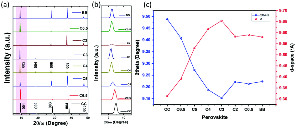 | ||
| Fig. 2 (a) Powder XRD patterns of Cu-perovskite crystals. (b) Expansion of XRD-first peak. (c) Relationship between 2θ/d-space values of XRD-first peak (y-axis) and mixed-halide perovskite crystals (x-axis). | ||
As illustrated in the AFM topographical map (Fig. 3(a)) on the (002) face of the C3 bulk single crystal, the perovskite material reveals a terrace feature with two-dimensional parallel large quantum well planes. Fig. 3(b–d) display the edge height difference for three different layers A, B, and C. The steps are 1.1, 1.1, and 1.2 nm, respectively, which are nearly equal to the d-space of the C3 perovskite (0.965 nm), suggesting that each layer resembles a single layer.
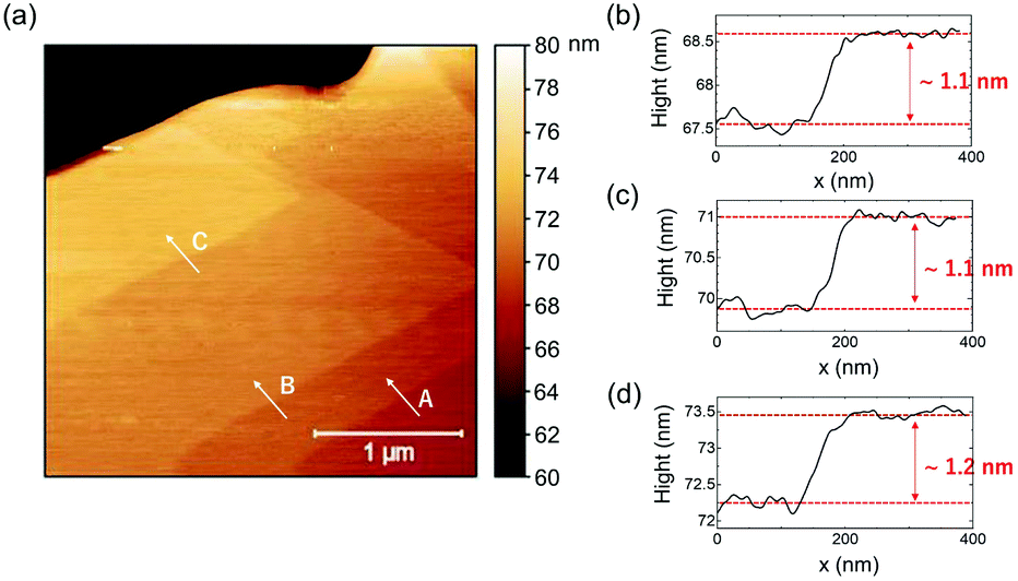 | ||
| Fig. 3 (a) AFM topography image of the C3 perovskite bulk single crystal on the (002) plane (scale bars: 1 μm). (b–d) Height profiles of three regions A–C, respectively, of C3 perovskite bulk single crystal along the (002) facet. | ||
Study of vibrational modes
To understand the structural origin of (CH3NH3)2CuCl4−xBrx single crystals, the important Raman spectral bands of mixed-halide perovskite single crystals were examined between 50 and 3400 cm−1. The Raman modes, as shown in Fig. 4(a), naturally separate into four different band regions, M1–M4, according to the nature of their molecular motion. The low-frequency range of Raman spectra (50–300 cm−1), with three main band regions M1, M2, and M3, are assigned to the internal and external modes of X–Cu–X bonds, where X: Cl or Br. The Raman bands in these regions are shifted towards higher Raman frequencies with the appearance of new features with a decrease in the weight of the halide derivatives, that is, in the Br–Cl sequence, which confirms not only the alloy nature of (CH3NH3)2CuCl4−xBrx crystals, but also the influence of the copper–halide interaction over the Raman peaks. A similar observation was also observed for mixed-halide lead-based perovskite single crystals, as reported by Ruan et al.37 In particular, the M1-Raman band region, ∼97 cm−1 for all bromide-perovskite (BB) samples, which may be assigned to the stretching vibration of the Cu–Br bond, is blue-shifted with an increase in Cl content until it disappears at C0.5 and CC samples. For all chloride perovskite single crystals (CC), the Raman modes at M1–167 and M2–238 cm−1 are ascribed to the equatorial and axial planar vibrations of Cu–Cl bonds, respectively.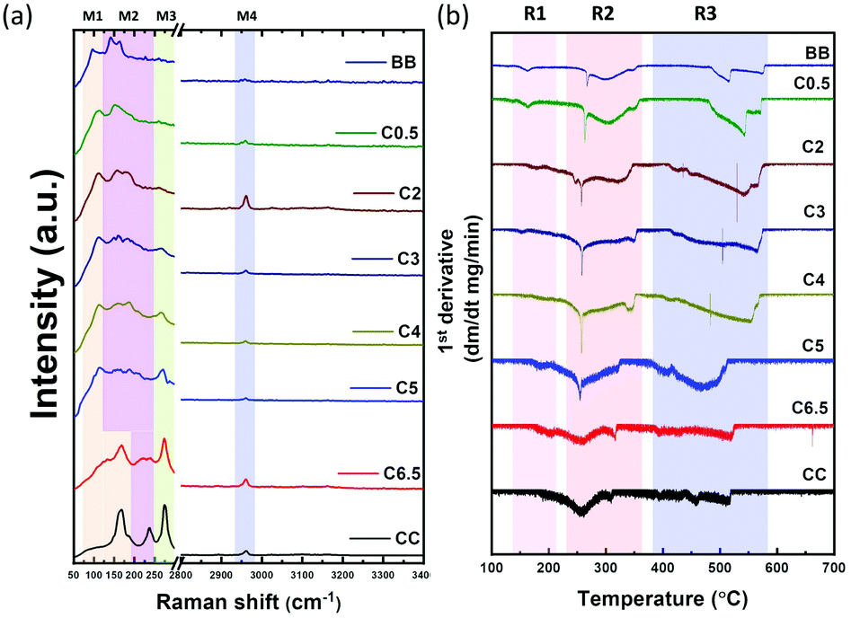 | ||
| Fig. 4 (a) Raman spectra of Cu-perovskite crystals. (b) First derivative of TGA analysis. | ||
In addition, the M3-Raman band region, ∼275 cm−1 for the CC sample, is assigned to both the bridging Cu–Cl vibration and out-of-phase coupling of the terminal Cu–Cl vibration. This band is shifted towards lower frequencies with Br-doping and is accompanied by band broadening and decreasing Raman intensities. It is worth noting that the widths of the Raman peaks at the (M1–M3) regions for mixed halide crystals are broader than those of CC or BB, which can be assigned to the microscopic disorder in (CH3NH3)2CuCl4−xBrx crystals.38 On the other hand, all perovskite crystals have the same high-frequency Raman peak in the M4 band region ∼2960 cm−1, which is attributed to the overlapping of the stretching vibration of hydrogen bonding between the halide and hydrogen of the organic ammonium cation N–H·X with the stretching vibration of C–H in the MA-cation.39
Thermal stability
Thermal stability was studied for mixed-halide Cu-perovskites through thermogravimetric analysis (TGA) for powder samples obtained by grinding single crystals. The decomposition profiles for Cu-perovskites can be divided into two steps, as shown in Fig. S6, ESI.† The first step (R1 and R2 regions) is composed of two partial steps of HX and CH3NH2 weight losses, respectively. The second step (R3 region) is possibly accompanied by the loss of CuX2.15 The first derivative peaks are plotted in Fig. 4(b). The first weight loss, as presented in the R1 region, shifted towards higher temperatures with increasing Cl content. At 167, 165, 159, 146, 122, 128, 117, and 90 °C for CC, C6.5, C5, C4, C3, C2, C0.5, and BB samples, respectively, which indicated an increase in thermal stability as the Cl content increased. The broader feature of the CC sample in the R1- and R2-regions of the 1st derivative suggests that the weight in the first weight loss step of the organic species MACl is not as readily lost as HCl and is more tightly bound into the perovskite structure, likely by hydrogen bonding. However, as the Br content increases, the sharp features obtained suggest that the two sequential partial weight loss steps, HX and organic species, respectively, became obvious. As previously reported, mixed halide systems tend to form an excess of organic material that undergoes sublimation upon heating of the perovskite, and as a result, an additional weight loss step is obtained in the TGA curve.40Optical properties
UV-Vis spectra in the diffuse reflectance mode measured the optical band gap energies using the reflectance data according to the Kubelka–Munk equation (Fig. 5(a) and (b)). The optical direct band gaps of the perovskites are 2.24 eV for CC, 2.12 eV for C6.5, 2.01 eV for C5, 1.99 eV for C4, 1.89 eV for C3, 1.47 eV for C2, 1.45 eV for C0.5, and 1.43 eV for BB. These tuning of the band gap energy values appear evident from the color of both the single crystals and the powders, which change from yellow to petroleum green on increasing the Br content. According to the literature, the (CH3NH3)2CuClxBr4−x series show strong absorption bands, with absorption coefficients of up to 35![[thin space (1/6-em)]](https://www.rsc.org/images/entities/char_2009.gif) 000 cm−1, with typical features of strong Jahn–Teller distortion in square planar coordinated copper complexes, CuX42−18
000 cm−1, with typical features of strong Jahn–Teller distortion in square planar coordinated copper complexes, CuX42−18
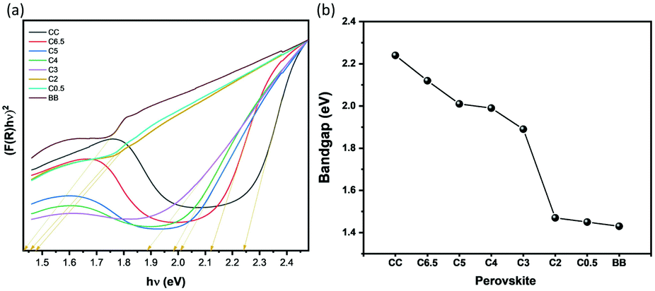 | ||
| Fig. 5 Band gap determination of Cu-perovskites (a) Kubelka–Munk function plot. (b) Band gap energy values of Cu-perovskite crystals extracted from the Kubelka–Munk function. | ||
Mechanical exfoliation
To further approve their two-dimensional structure, a mechanical exfoliation process was performed using a SiO2/Si substrate and Nitto tape. All mixed-halide Cu-perovskites were mechanically exfoliated to obtain 2D flakes with different thicknesses. Fig. 6(a) shows the microscopic optical images of the (CH3NH3)2CuCl4 Cu-perovskite (CC) flakes. The difference in the flake colors through these optical images is an indication of both the successful exfoliation process and the difference in thickness. To further verify the difference in thickness, Raman spectral bands of different flakes were examined between 50 and 3400 cm−1. For the 50–450 cm−1 range as shown in Fig. 6(b), the exfoliation process led to a decrease in the intensity of the three main vibrational bands of perovskite flakes (black dashed lines) and an increase in the intensity of the Raman peak of the Si at nearly 300 cm−1 (the red dashed line) with peak broadening as the thickness of the flake decreases. According to the 2500–3000 cm−1 range, as shown in Fig. 6(c), the 2960 cm−1 vibrational band intensity decreased with exfoliation until the disappearance of the light purple flake, which may be an indication of the breakdown of hydrogen bonding between the halide and hydrogen of the organic ammonium cation N–H·X for the lowest exfoliated flake. Other samples of mixed halide and all bromide copper perovskites were successfully exfoliated and showed the same behavior as all chloride perovskite flakes, as shown in Fig. S7–S13, ESI.† These findings require further investigation to study the impact of exfoliation of Cu-perovskites on their optoelectronic properties. | ||
| Fig. 6 Exfoliation effect: (a) Optical microscopy images of different mechanically exfoliated MA2CuCl4 flakes, scale bar (10 μm). (b) The position of the incident laser beam is circled in black, (c) Raman spectra of exfoliated flakes in the range of 50–50 cm−1 and 2500–3000 cm−1, respectively. | ||
Thermochromic behavior
All mixed-halide Cu-perovskites showed reversible thermochromism. We attempted to track the thermochromic effect using both microscopic cameras and temperature-dependent XRD measurements. Reversible thermochromism was investigated using a microscopic camera through heating–cooling cycles for Cu-perovskite single crystals. Reversible thermochromic processes of all mixed-halide perovskites are presented in the ESI.† Fig. S7 of the ESI,† shows the microscopic camera photographs of mixed-halide Cu perovskite crystals at high temperatures. When comparing the crystals at room temperature and high temperature, there was an obvious color change for Cl-rich perovskites, as shown in Fig. 7(a–f). However, there was no observable color change for Br-rich perovskite materials, as shown in Fig. 7(g and h). | ||
| Fig. 7 Microscopy images of (a) CC, (b) C6.5, (c) C5, (d) C4, (e) C3, (f) C2, (g) C0.5, and (h) BB, scale bar (1 mm) at high temperatures. | ||
Based on results of Differential Scanning Calorimetry (DSC) analysis, as shown in the ESI,† Fig. S29 and S30, which was performed for mixed-halide Cu-perovskites from 300 K to 380 K with the heating/cooling cycle. Only Cl-rich samples (CC, C6.5, and C5) showed structural phase transition with endothermic peaks at 348.5, 350.5, and 350.3 K, respectively. However, the remaining Br-rich samples showed no structural phase transition except the C0.5 sample with very small endothermic peak at 354 K.
Thermochromism for all mixed-halide Cu-perovskites was further examined by temperature-dependent XRD measurements. Initially, temperature-dependent XRD was tracked in the range of a 30–80 °C heating–cooling cycle for the C6.5 sample. Dramatic changes for d-space values were observed above 70 °C, as shown in Fig. S15 and S16 (ESI†), which indicates structural phase transition, consistent with DSC results. Consequently, the temperature was controlled in the range of 30–60 °C during XRD measurement under the effect of heating/cooling cycles for the remaining samples. As shown in Fig. S15–S28 (ESI†), for all mixed-halide Cu-perovskites, during the heating step from 30 to 60 °C, the XRD peaks shifted to lower 2θ angles. During the cooling step from 60 to 30 °C, the XRD peaks shifted back to the higher 2θ angles. These results indicate that only crystal lattice expansion, no structural phase transition, occurs in the crystal upon heating in the range 30–60 °C, which is consistent with the DSC results.
Fig. 8(a) and (b) show the microscopic camera photographs of the CC crystal under the effect of heating and cooling, respectively. The yellow color of the CC sample changed upon heating to dark yellow and changed back to its original yellow color upon cooling. The darkness of the crystal is an indication of band gap reduction. The thermochromism for CC was examined with temperature-dependent XRD measurements (see Fig. S14, ESI,† for full range XRD). Fig. 8(c) shows that the diffraction peak at 2θ = 38.018 shifted to lower 2θ angles (2θ = 37.957 at 60 °C) upon increasing the temperature, and gradually shifted back to higher 2θ values during the cooling process. The crystal structure of CC upon heating and cooling is visualized by comparing the d-lattice spacing parameters at each temperature, as shown in Fig. 8(d). The results show that the d-spacing increased upon heating and decreased upon cooling, showing a reversible process. It should be noted that the peak position did not fully recover to its original position after one heating/cooling cycle, which can be an indication of slight hysteresis. Similar hysteresis has been previously reported for 2D (BED)2CuCl618 and 3D (CH3NH3)PbI341 perovskites.
 | ||
| Fig. 8 (a and b) Temperature-induced color change of the CC crystal with heating and cooling cycles. Temperature-dependent XRD of CC: (c) Expansion of 2θ = 38.1° reflection at different temperatures. (d) d-spacing calculated from the 2θ values extracted from the XRD patterns at different temperatures. | ||
Temperature-dependent transmittance spectra were collected for the heating/cooling cycle in the range of 30–60 °C for exfoliated mixed-halide Cu-perovskites (Fig. S31–S34, ESI†) to further confirm thermochromic behavior. Upon heating, all perovskites samples showed shifting of the transmittance edges towards longer wavelengths, narrowing the band gap. On the other hand, upon cooling, shifting of the transmittance edges back toward shorter wavelengths, and widening of the band gap were observed. The red/blue shifts of the transmittance edges during heating/cooling cycles, respectively, are consistent with the darkness of the color upon heating and reversing-back to its original color upon cooling. Moreover, these results confirm reversible thermochromism in 2D-mixed-halide Cu perovskites after mechanical exfoliation. Hysteresis loops of transmittance values at different temperature values, provided in the ESI,† are also consistent with hysteresis obtained from temperature-dependent XRD.
Conclusions
In summary, we have synthesized centimeter-sized 2D mixed-halide Cu-based perovskite crystals via a slow evaporation method and studied their structural, thermal, and optical properties and their exfoliation and thermochromism. All crystals displayed a strong orientation along the c-axis direction with preferable (00l) diffraction peaks. The thermal stability of perovskites increased as the Cl content increased. As the Br content increases, mixed-halide Cu-perovskites exhibit a tunable band gap energy ranging from 2.24 eV to 1.43 eV. Upon temperature variation, mixed-halide perovskites show a reversible thermochromic behavior indicated by the darkness of their color. The in situ temperature-dependent XRD confirmed this color change by tracking of 2θ reflections and lattice spacing values of temperature-induced crystals.Author's contributions
Amr Elattar and Yasuhiko Hayashi conceived the idea for the manuscript and designed the experiments. Amr Elattar, Ryuji Mishima and Nakao Kodai synthesized the materials and conducted structural and optical characterization. Amr Elattar and Hiroo Suzuki conducted Raman and AFM measurements. Ryuji Mishima and Hiromi Ota carried out the temperature-dependent PXRD characterization. Amr Elattar carried out temperature-dependent transmittance measurements. Hirotaka Inoue carried out DSC measurements. Amr Elattar, Hiroo Suzuki, Takeshi Nishikawa, Aung Ko Ko Kyaw, and Yasuhiko Hayashi discussed the results and commented on the manuscript at all stages. Yasuhiko Hayashi led the project.Conflicts of interest
There are no conflicts to declare.Acknowledgements
We would like to thank Editage (http://www.editage.com) for English language editing. A. E. acknowledges financial support from the Egypt-Japan Education Partnership (EJEP) for his PhD scholarship and Ain Shams University (Cairo, Egypt) for supporting the research.References
- N. Wang, L. Cheng, R. Ge, S. Zhang, Y. Miao, W. Zou, C. Yi, Y. Sun, Y. Cao, R. Yang, Y. Wei, Q. Guo, Y. Ke, M. Yu, Y. Jin, Y. Liu, Q. Ding, D. Di, L. Yang, G. Xing, H. Tian, C. Jin, F. Gao, R. H. Friend, J. Wang and W. Huang, Nat. Photonics, 2016, 10, 699–704 CrossRef CAS.
- W. Zou, R. Li, S. Zhang, Y. Liu, N. Wang, Y. Cao, Y. Miao, M. Xu, Q. Guo, D. Di, L. Zhang, C. Yi, F. Gao, R. H. Friend, J. Wang and W. Huang, Nat. Commun., 2018, 9, 608 CrossRef.
- H. Zhang, Q. Liao, Y. Wu, Z. Zhang, Q. Gao, P. Liu, M. Li, J. Yao and H. Fu, Adv. Mater., 2018, 30, 1706186 CrossRef.
- Y. Pan, H. Wang, X. Li, X. Zhang, F. Liu, M. Peng, Z. Shi, C. Li, H. Zhang, Z. Weng, M. Gusain, H. Long, D. Li, J. Wang, Y. Zhan and L. Zheng, J. Mater. Chem. C, 2020, 8, 3359–3366 RSC.
- J. Wang, C. Zhang, H. Liu, R. McLaughlin, Y. Zhai, S. R. Vardeny, X. Liu, S. McGill, D. Semenov, H. Guo, R. Tsuchikawa, V. V. Deshpande, D. Sun and Z. V. Vardeny, Nat. Commun., 2019, 10, 129 CrossRef.
- X. Pan, H. Liu, U. Huynh and Z. V. Vardeny, J. Chem. Phys., 2020, 152, 44714 CrossRef CAS.
- S. Chatterjee and A. J. Pal, J. Mater. Chem. A, 2018, 6, 3793–3823 RSC.
- X.-G. Zhao, J.-H. Yang, Y. Fu, D. Yang, Q. Xu, L. Yu, S.-H. Wei and L. Zhang, J. Am. Chem. Soc., 2017, 139, 2630–2638 CrossRef CAS.
- Z. Zhao, F. Gu, Y. Li, W. Sun, S. Ye, H. Rao, Z. Liu, Z. Bian and C. Huang, Adv. Sci., 2017, 4, 1700204 CrossRef.
- W. Meng, X. Wang, Z. Xiao, J. Wang, D. B. Mitzi and Y. Yan, J. Phys. Chem. Lett., 2017, 8, 2999–3007 CrossRef CAS.
- L. Qian, Y. Sun, M. Wu, C. Li, D. Xie, L. Ding and G. Shi, Nanoscale, 2018, 10, 6837–6843 RSC.
- D. Ray, C. Clark, H. Q. Pham, J. Borycz, R. J. Holmes, E. S. Aydil and L. Gagliardi, J. Phys. Chem. C, 2018, 122, 7838–7848 CrossRef CAS.
- I. Zimmermann, S. Aghazada and M. K. Nazeeruddin, Angew. Chem., Int. Ed., 2019, 58, 1072–1076 CrossRef CAS.
- R. L. Z. Hoye, R. E. Brandt, A. Osherov, V. Stevanović, S. D. Stranks, M. W. B. Wilson, H. Kim, A. J. Akey, J. D. Perkins, R. C. Kurchin, J. R. Poindexter, E. N. Wang, M. G. Bawendi, V. Bulović and T. Buonassisi, Chem. – Eur. J., 2016, 22, 2605–2610 CrossRef CAS.
- D. Cortecchia, H. A. Dewi, J. Yin, A. Bruno, S. Chen, T. Baikie, P. P. Boix, M. Grätzel, S. Mhaisalkar, C. Soci and N. Mathews, Inorg. Chem., 2016, 55, 1044–1052 CrossRef CAS.
- A. M. Elseman, A. E. Shalan, S. Sajid, M. M. Rashad, A. M. Hassan and M. Li, ACS Appl. Mater. Interfaces, 2018, 10, 11699–11707 CrossRef CAS.
- J. Li, X. Liu, P. Cui, J. Li, T. Ye, X. Wang, C. Zhang and Y. S. Zhao, Sci. China: Chem., 2019, 62, 1257–1262 CrossRef CAS.
- B. Sun, X.-F. Liu, X.-Y. Li, Y. Cao, Z. Yan, L. Fu, N. Tang, Q. Wang, X. Shao, D. Yang and H.-L. Zhang, Angew. Chem., Int. Ed., 2020, 59, 203–208 CrossRef CAS.
- P. Pandey, N. Sharma, R. A. Panchal, S. W. Gosavi and S. Ogale, ChemSusChem, 2019, 12, 3742–3746 CrossRef CAS.
- R. Willett, H. Place and M. Middleton, J. Am. Chem. Soc., 1988, 110, 8639–8650 CrossRef CAS.
- L. O. Snively, J. E. Drumheller and K. Emerson, Phys. Rev. B: Condens. Matter Mater. Phys., 1981, 23, 6013–6017 CrossRef CAS.
- A. Aqeel, N. Akhtar, A. O. Polyakov, P. Rudolf and T. T. M. Palstra, APL Mater., 2018, 6, 114206 CrossRef.
- Z. Hu, H. Zhao, Z. Cheng, J. Ding, H. Gao, Y. Han, S. Wang, Z. Xu, Y. Zhou, T. Jia, H. Kimura and M. Osada, Phys. Chem. Chem. Phys., 2020, 22, 4235–4239 RSC.
- L. J. de Jongh, J. Appl. Phys., 1978, 49, 1305–1310 CrossRef CAS.
- W. E. Estes, D. B. Losee and W. E. Hatfield, J. Chem. Phys., 1980, 72, 630–638 CrossRef CAS.
- A. O. Polyakov, A. H. Arkenbout, J. Baas, G. R. Blake, A. Meetsma, A. Caretta, P. H. M. van Loosdrecht and T. T. M. Palstra, Chem. Mater., 2012, 24, 133–139 CrossRef CAS.
- K. Leng, W. Fu, Y. Liu, M. Chhowalla and K. P. Loh, Nat. Rev. Mater., 2020, 5, 482–500 CrossRef CAS.
- Y. Huang, E. Sutter, N. N. Shi, J. Zheng, T. Yang, D. Englund, H.-J. Gao and P. Sutter, ACS Nano, 2015, 9, 10612–10620 CrossRef CAS.
- W. Niu, A. Eiden, G. V. Prakash and J. J. Baumberg, Appl. Phys. Lett., 2014, 104, 171111 CrossRef.
- B. Dhanabalan, A. Castelli, M. Palei, D. Spirito, L. Manna, R. Krahne and M. Arciniegas, Nanoscale, 2019, 11, 8334–8342 RSC.
- X.-D. Wang, N.-H. Miao, J.-F. Liao, W.-Q. Li, Y. Xie, J. Chen, Z.-M. Sun, H.-Y. Chen and D.-B. Kuang, Nanoscale, 2019, 11, 5180–5187 RSC.
- V. A. Hintermayr, A. F. Richter, F. Ehrat, M. Döblinger, W. Vanderlinden, J. A. Sichert, Y. Tong, L. Polavarapu, J. Feldmann and A. S. Urban, Adv. Mater., 2016, 28, 9478–9485 CrossRef CAS.
- W. Zhang, Y. Sui, B. Kou, Y. Peng, Z. Wu and J. Luo, ACS Appl. Mater. Interfaces, 2020, 12, 9141–9149 CrossRef CAS.
- J. Li, J. Wang, Y. Zhang, H. Wang, G. Lin, X. Xiong, W. Zhou, H. Luo and D. Li, 2D Mater., 2018, 5, 021001 CrossRef.
- B. Dhanabalan, Y.-C. Leng, G. Biffi, M.-L. Lin, P.-H. Tan, I. Infante, L. Manna, M. P. Arciniegas and R. Krahne, ACS Nano, 2020, 14, 4689–4697 CrossRef CAS.
- W. Wang, J. Su, L. Zhang, Y. Lei, D. Wang, D. Lu and Y. Bai, CrystEngComm, 2018, 20, 1635–1643 RSC.
- S. Ruan, D. P. McMeekin, R. Fan, N. A. S. Webster, H. Ebendorff-Heidepriem, Y.-B. Cheng, J. Lu, Y. Ruan and C. R. McNeill, J. Phys. Chem. C, 2020, 124, 2265–2272 CrossRef CAS.
- F. Liu, F. Wang, K. R. Hansen and X.-Y. Zhu, J. Phys. Chem. C, 2019, 123, 14865–14870 CrossRef CAS.
- N. Meinander, G. Bergström, S. Forss and F. Stenman, J. Raman Spectrosc., 1979, 8, 265–273 CrossRef CAS.
- A. Dualeh, P. Gao, S. Il Seok, M. K. Nazeeruddin and M. Grätzel, Chem. Mater., 2014, 26, 6160–6164 CrossRef CAS.
- A. Osherov, E. M. Hutter, K. Galkowski, R. Brenes, D. K. Maude, R. J. Nicholas, P. Plochocka, V. Bulović, T. J. Savenije and S. D. Stranks, Adv. Mater., 2016, 28, 10757–10763 CrossRef CAS.
Footnote |
| † Electronic supplementary information (ESI) available. See DOI: 10.1039/d0tc04307a |
| This journal is © The Royal Society of Chemistry 2021 |