
2D layered metal-halide perovskite/oxide semiconductor-based broadband optoelectronic synaptic transistors with long-term visual memory†
Youngjun
Park
,
Min-Kyu
Kim
and
Jang-Sik
Lee
 *
*
Materials Science and Engineering, Pohang University of Science and Technology (POSTECH), Pohang 37673, Korea. E-mail: jangsik@postech.ac.kr; Tel: +82 54-279-2153
First published on 5th January 2021
Abstract
To implement neuromorphic visual systems that can perceive and memorize optical information, it is essential to realize the artificial synapses that respond to optical signals. Organic–inorganic halide perovskites (OIHPs) have been considered as optically modulated synapses due to high absorption coefficient and long charge-carrier lifetime. However, it is difficult to store the optical information because photo-excited carriers recombine after removal of illumination. Here, we combine an OIHP with indium zinc tin oxide (IZTO) to implement artificial synapses that can perceive and memorize optical information for long-term storage in neuromorphic visual systems. The transparent IZTO on OIHP allows optical signal absorption by the OIHP and protects it from atmosphere exposure. Excellent optical absorption of OIHP leads to generation of photo-excited carriers, and the band alignment between IZTO and OIHP facilitates the spatial separation of photo-excited carriers that serves as the basis of optically-meditated charge trapping; these characteristics enable nonvolatile change in conductance. Optical synapses show potentiation/depression under multiple wavelengths with a large dynamic range of ∼104, which is significantly advantageous for recognition accuracy in artificial neural networks. These results demonstrate the feasibility of OIHP-based optical synapses for neuromorphic visual systems.
Introduction
Vision is the main sense by which humans perceive their environment.1,2 Optical information sensed by the retina is transmitted and interpreted by neural networks.3 In neural networks, synapses are the basic units that transmit, process, and memorize visual information.3 These processes can be achieved by synaptic plasticity, which is a change of connection strength of a synapse in response to repeated stimulation, in this case by light signals.4 Therefore, the implementation of neuromorphic visual systems requires emulation of this synaptic plasticity in response to the optical stimuli. For this purpose, artificial synapses for vision perception have been designed by connecting a photodetector to a memory device,5–7 but this physical separation of the optical sensing and memory requires complex integrated circuits that cause low efficiency and high power consumption. The solution to this problem is to develop a device that can perform detection and synaptic behaviors simultaneously.To implement such artificial synapses, various materials have been evaluated using graphene, quantum dots, transition metal dichalcogenides, and organic–inorganic halide perovskites (OIHPs).8–12 Especially, OIHPs have superior optical properties such as high optical absorption coefficient, long carrier diffusion length, and low exciton binding energy, and therefore have been considered as promising candidates for artificial synapses.8,13–18 However, OIHPs are easily degraded by air and moisture.19,20 Two-dimensional (2D) layered OIHPs have been evaluated to overcome these problems.21–23 2D layered OIHPs can be regarded as derivatives of 3D OIHPs by replacing a small methylammonium cation (MA+) with a large ammonium cation such as butylammonium (BA+) or phenylethylammonium (PEA+).22,24 These OIHPs are stable in ambient air because the large cations can impede moisture infiltration.22 Also, the optical and electrical properties of 2D layered OIHPs can be easily modulated by modifying their compositions.23,25 However, although OIHPs have superior optical properties, they show only temporary change in conductance under illumination; and after removal of the illumination, the changed conductance decays rapidly due to recombination of photo-excited carriers.26,27 These properties impede applications of OIHPs as artificial synapses that require combined memory and learning functions. Thus, to store the information about optical stimulation, OIHPs have been developed as artificial synapses by introducing integrated structures with other materials such as pentacene with a floating-gate structure or Si nanomembrane.13,18,28,29 Synaptic behaviors in these devices result from the movement and trapping of photo-excited carriers between perovskite and channel layer. Also, to apply the artificial synapses to artificial neural networks (ANNs), the synapses should have large dynamic range (i.e., the ratio of maximum conductance to minimum conductance) and linear/symmetric synaptic weight updates. These properties would enable the implementation of ANNs with high recognition accuracy,30,31 so to obtain these properties, the development of materials and device structures for artificial synapses is required.
In this study, we develop an optical synapse that combines 2D layered OIHP of (C4H9NH3)2PbBr4 (BA2PbBr4, BA = butylammonium) with transparent oxide semiconductor of indium zinc tin oxide (IZTO). The use of IZTO on OIHP enables implementation of bottom-gate structure. In this optical synapse, the OIHP shows strong optical absorption, and therefore can be efficiently stimulated by optical spikes. The band alignment between IZTO and 2D layered OIHP can lead to the effective spatial separation of photo-excited carriers that serves as the basis of optically meditated charge trapping, which enables nonvolatile conductance change. The device shows potentiation/depression characteristics with a large dynamic range of ∼104. The large dynamic range can allow a large number of distinct synaptic weight states, which can improve the recognition accuracy in ANNs.31 Also, the large dynamic range can increase mapping capability of synaptic weights in algorithms that normalize synaptic weights to a range between 0 and 1.30 Symmetry and linearity of potentiation/depression characteristics are improved by controlling depression pulses. In a simulation using these properties, ANNs that use these optical synapses achieve 80% recognition accuracy of handwritten digits. These results demonstrate the feasibility of an optical synapse based on 2D layered OIHP and provide a promising resource for development of neuromorphic visual systems.
Experimental section
Materials
Lead bromide (PbBr2, 98% purity) was purchased from Sigma-Aldrich. n-Butylammonium bromide (BABr) was purchased from GreatCell Solar. Si wafers with a 300 nm-thick thermally-grown SiO2 were used as the substrate.Device fabrication
SiO2/Si substrate was cleaned by sequential ultrasonication in acetone, ethanol, and distilled water for 10 min each. The OIHP layer was formed by sequential vapor deposition. First, PbBr2 thin film was deposited on the substrate by thermal evaporation using PbBr2 powder. Then, the PbBr2 film deposited on the substrate was transferred to a glove box. To transform the PbBr2 to BA2PbBr4, PbBr2 film was exposed to BABr vapor that was prepared by heating the BABr powder (3 mg) sprinkled on a glass Petri dish. BaBr molecules were intercalated into PbBr2 frames during exposure to BABr vapor; consequently, the PbBr2 layer was transformed to BA2PbBr4 with layered structure. This treatment was performed at 150 °C for 3 h on a hot plate. Then IZTO film was deposited on the OIHP layer by co-sputtering from ITO and ZnO targets. The RF power of 100 W was used for the ZnO target, and DC power of 100 W was used for the ITO target. Sputtering was performed with the gas flow of Ar/O2 (10/4 sccm) at the deposition pressure of 5 mTorr. Finally, Al source and drain electrodes of 100 nm thickness were deposited on the IZTO layer by e-beam evaporation.Characterization
All electrical characteristics of the optical synapse were measured using a semiconductor parameter analyser (4200A-SCS, Keithley) in the probe station. The crystal structures of PbBr2 and 2D layered OIHP were investigated using X-ray diffraction (XRD, D/MAX-2500, Rigaku) with Cu Kα radiation. The optical responses were measured by applying monochromatic light from a xenon lamp under ambient conditions with a light source (Model 71SI00059, Newport). Memorization of letter ‘N’ images by the optical synapse array was performed by optical spike input to each device in a 5 × 5 synapse array.Results and discussion
A human perceives optical information via the retina (Fig. 1a). Nerve cells in a retina transform optical information to neural impulses, which are transmitted along the optic nerve to the visual cortex in the brain.3 The visual cortex consists of a large number of neurons and synapses that can process and memorize information.3,32 We emulated these properties of a visual system by implementing optical synapses composed of 2D layered BA2PbBr4 and IZTO. The BA2PbBr4 was composed of an inorganic layer of [PbBr6]4− octahedra sandwiched between two organic [C4H9NH3]+ layers (Fig. 1b). The BA2PbBr4 was formed by sequential vapor deposition of PbBr2 and BABr on SiO2/Si substrate (Fig. 1c).33 This process could form an OIHP layer that has uniform surface coverage and controllable thickness.34,35 A PbBr2 layer was first deposited on the substrate by thermal evaporation. Then BABr was deposited on the PbBr2 layer to form the BA2PbBr4. BaBr molecules became intercalated into the PbBr2 frames during this process, then PbBr2 was transformed to BA2PbBr4. To confirm the formation of BA2PbBr4 OIHP, we analyzed the XRD patterns. The XRD patterns of BA2PbBr4 showed (00l) diffraction peaks, which indicated the preferential orientations along c-axis (Fig. 1d).33,36 To confirm whether sputtering of IZTO affects the quality of the OIHP, we analyzed the XRD patterns of BA2PbBr4 after the deposition of IZTO. Diffraction peaks assigned to (002), (004), (006), (008), and (0010) planes were observed (Fig. S1, ESI†); this result is consistent with the peaks observed on the BA2PbBr4 film before deposition of IZTO. These results indicated that the sputtering process did not noticeably affect the OIHP film.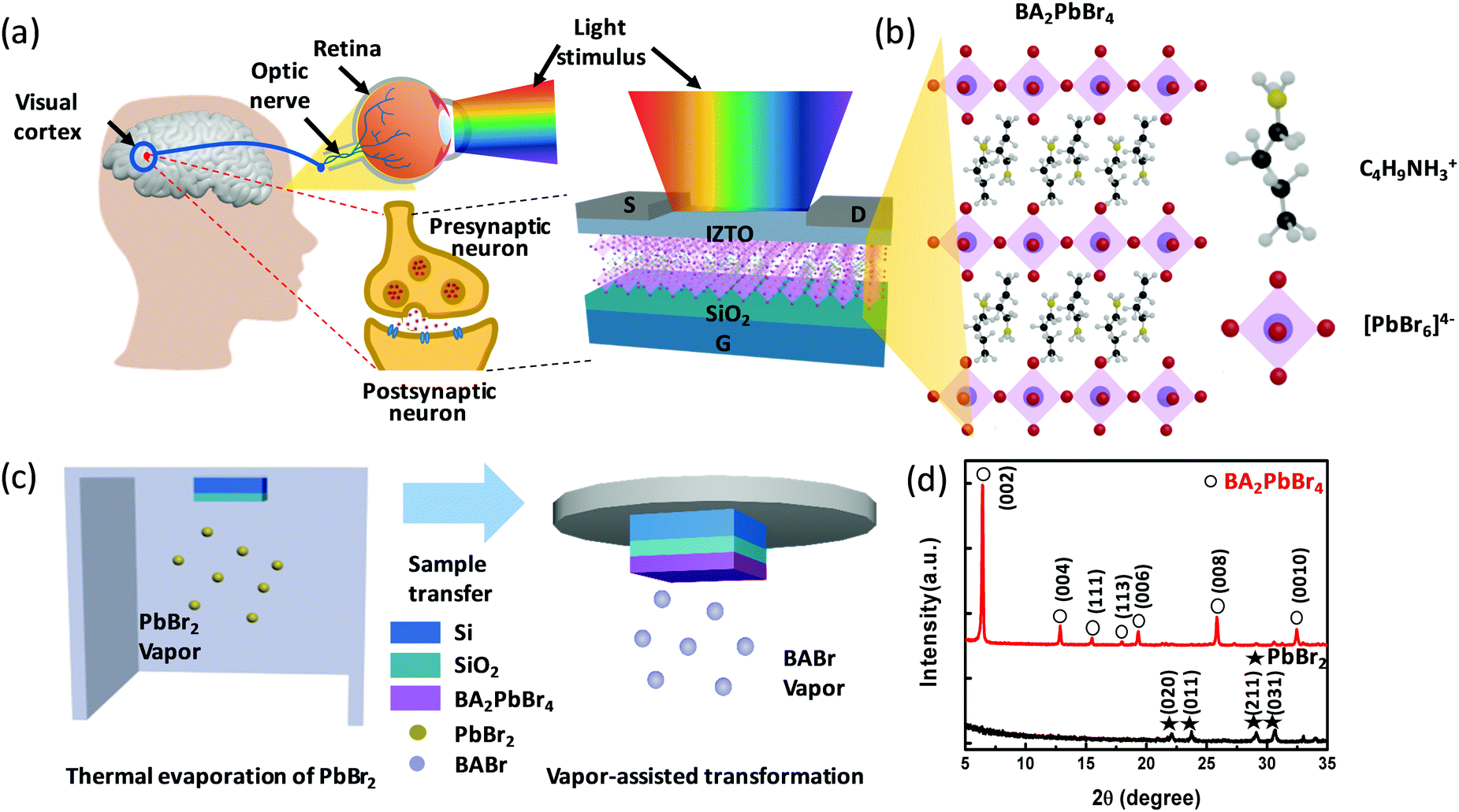 | ||
| Fig. 1 (a) Schematic illustrations of human visual system and optical synapse composed of 2D layered OIHP with IZTO. Al is used for source (S) and drain (D) electrodes; Si is used as the gate electrode (G). (b) Schematic structure of BA2PbBr4 (atom colors: Pb = blue; Br = red; C = black; N = yellow; H = grey). (c) Schematic illustrations of procedures to deposit the 2D layered OIHP using the sequential vapor deposition process. PbBr2 film is deposited by thermal evaporation, then this PbBr2 film is exposed to BaBr vapor to convert PbBr2 to BA2PbBr4. (d) XRD patterns of PbBr2 and BA2PbBr4. | ||
The transfer characteristics of the device were measured by applying gate voltage VG to the Si gate electrode under a drain voltage VD of 5 V. When an optical pulse with a wavelength λ = 365 nm and intensity LI = 100 μW cm−2 was irradiated to the device for 30 s, drain current ID abruptly increased and the threshold voltage shifted in the negative direction. (Fig. 2a). The threshold voltage was changed more in the device that combined IZTO with 2D layered OIHP than in the device that used only IZTO (Fig. S2, ESI†). These results indicated that electron–hole pairs generated by light illumination in the OIHP layer could contribute to the device operation. Transfer curve that shifted in the negative direction returned to its initial state after the application of a positive VG pulse (30 V, 2 s). To further quantify the effect of illumination, the device was exposed to light (365 nm, 100 μW cm−2) for 30 s, without applying VG (i.e., VG = 0 V). The ID increased abruptly from high-resistance state (HRS) to low-resistance state (LRS) during illumination; and the ratio of the current values of the two states was ∼104 (Fig. 2b). The device remained in LRS for 104 s after the illumination ceased (Fig. S3, ESI†). The long retention time may be related to optically-meditated charge trapping, so it is important to understand charge trapping mechanism and trap energy levels. The trap depth can be calculated from attempt-to-escape frequencies and trap density of states obtained by thermal admittance spectroscopy measurement.37–39 Among them, the attempt-to-escape frequency can be obtained by temperature-dependent capacitance-frequency measurement.38,40 Deep-level traps may be formed for long retention time. 2D layered OIHPs are known to have deep level defects.41,42 Butylammonium-based 2D layered OIHP has deep level defects with a defect activation energy of 0.398 eV, which is higher than that of 3D perovskite (0.075 eV).42 In our device, 2D layered OIHP was used for optical signal absorption and the formation of deep traps in the 2D layered OIHP may enable long retention time. Also, we implemented four distinct resistance states by controlling light illumination time (Fig. 2c). These results demonstrated that the device showed the feasibility of multilevel data storage by modulating the illumination time. In addition, the device showed consecutive resistance change between HRS and LRS during repeated application of pulses. The change of resistance from HRS to LRS was achieved by an optical pulse (365 nm, 100 μW cm−2, 10 s). The return to HRS from LRS was implemented by applying a VG pulse (30 V, 2 s) (Fig. 2d). The 2D layered OIHP-based device was switched stably between HRS and LRS for 110 cycles (Fig. 2e). To confirm the stability, the device was kept in ambient air and transfer characteristics were measured. The device was operated stably without degradation after 14 days (Fig. S4, ESI†). There are several possible mechanisms for device operation in three-terminal devices such as ion migration and charge carrier transport. OIHP film includes several ions such as CH3NH3+, Pb2+, and halides.43 In 3D OIHP, halide ions can move easily because they have a low ionic migration barrier.44,45 However, in 2D OIHP, ion migration is suppressed because long-chain organic cations can act as a barrier that prevents the ion migration.46,47 Also, ion migration in the OIHP is observed when voltage is applied and affects the electrical properties of device.48,49 However, the fabricated device did not require the voltage to change the resistance from HRS to LRS. In contrast, movement of photo-excited carriers can affect the change of resistance state of device. The change of resistance state with optical signal may be a result of the photogating effect caused by photo-excited carriers.50 The photogating effect has been reported in heterostructured devices that combine OIHP with oxide semiconductor, organic semiconductor, or graphene.12,13,50–53 During light illumination, electron–hole pairs were generated in the 2D OIHP layer (Fig. 2f). The photo-excited carriers could be effectively dissociated by the built-in field that was induced by a bending of the energy band. The photo-excited electrons were transferred from OIHP layer to IZTO layer, whereas the photo-excited holes remained behind in OIHP layer. These holes could induce photogating effect and consequently increase current by capacitive coupling.50 The number of remaining holes could be reduced by recombination under positive VG, and thereby overcome the barrier to prompt electron injection from IZTO to OIHP layer, so the increased ID could return to its initial state.
 | ||
| Fig. 2 (a) Transfer characteristics of the device in ‘dark’, ‘after illumination’, and ‘erase’ operation. Transfer characteristic of ‘after illumination’ state is measured 30 s after application of optical pulse (365 nm, 100 μW cm−2, 30 s) under VG sweep from −15 to 5 V. Transfer characteristic of ‘erase’ state is measured after applying a positive VG pulse (30 V, 2 s) under VG sweep from 5 to 20 V. (b) Retention property after light illumination for 30 s. (c) Change of ID with different durations of illumination (5 s, 10 s, 30 s) and without illumination. (d) The resistance change of the device by applying optical spikes (365 nm, 100 μW cm−2, 10 s) and applying positive VG (30 V, 2 s). (e) Change of ID between LRS and HRS for 110 cycles. (f) Schematic illustration of band diagram of the IZTO/2D layered OIHP device under illumination. | ||
Synapses are responsible for signal transmission, memory, and learning functions in a brain.54 Biological synapses are located between presynaptic and postsynaptic neurons. The synapses perform their functions by adapting their connection strength, which is called ‘synaptic plasticity’.55,56 Synaptic plasticity can be classified into short-term plasticity (STP) and long-term plasticity (LTP).57,58 STP is a temporary change in synaptic weight that lasts a few seconds to minutes; LTP is a permanent change in synaptic weight that lasts days to years.58 We emulated synaptic plasticity by using the device. STP was emulated by applying an optical pulse with a short pulse duration that was insufficient to induce a permanent change of current. When optical pulses (365 nm, 100 μW cm−2) with a duration of 50 ms were applied, the ID increased, then decayed after the applied pulses ended (Fig. 3a). Also, we emulated paired-pulse facilitation (PPF) using the device. PPF is the phenomenon in which a second presynaptic spike causes a larger postsynaptic current than the first spike does.59 The degree of increase in the second postsynaptic current decreases with an increase in the time interval Δt between the two spikes. A biological synapse exploits PPF to recognize and decode temporal information.60 To emulate this characteristic, we applied two consecutive optical pulses (365 nm, 100 μW cm−2, 200 ms) with Δt = 400 ms. The first spike yielded an increased amplitude A1 of ID, and the second spike yielded a further increased amplitude A2 (Fig. 3b). Also, we investigated the change of PPF value by adjusting Δt between two pulses. The PPF index was defined as a ratio between A2 and A1 (A2/A1 × 100%).60 The PPF index was 55% at Δt = 100 ms, and decreased to 21% at Δt = 2 s (Fig. 3c). The decay in PPF index was described using a double-exponential function,61,62

 | ||
| Fig. 3 (a) STP characteristics with four consecutive optical spikes (365 nm, 100 μW cm−2, 50 ms). (b) Change of ID after two consecutive optical pulses (365 nm, 100 μW cm−2, 200 ms) separated by Δt = 400 ms. A1 is the change of ID after the first spike; A2 is the change of ID after the second spike. (c) Decrease in PPF = A2/A1 × 100% with increase in time interval Δt between two optical spikes. (d) LTP characteristics by four consecutive optical spikes (365 nm, 100 μW cm−2, 1 s) (e) Change of ID by the number of applied optical spikes (N = 5, 10, 20, 50). (f) Potentiation and depression characteristics of the ITZO/2D layered OIHP device. 50 optical spikes (100 μW cm−2, 1 s) with different wavelengths were applied for potentiation process and 50 positive VG pulses (20 V, 2 s) were applied for depression process. | ||
The goal in developing artificial synapses is to apply the devices to practical ANNs. The introduction of artificial synapses with weight-update characteristics can accelerate the training process and reduce power consumption in ANNs.65 Simulation can easily confirm the possibility of the fabricated device in practical application. We performed simulation to confirm the applicability of the fabricated artificial synapses in ANNs. To investigate the learning capability of the artificial synapse driven by optical spikes, we simulated the recognition accuracy in ANNs. The simulation was conducted using a multilayer perceptron neural network with 400 input neurons, 100 hidden neurons, and 10 output neurons (Fig. 4a).64,66 The Modified National Institute of Standard and Technology (MNIST) data set was used for the simulation. The multilayer perceptron algorithm was used in simulations with our experimental results of the optical synapse, including dynamic range, number of states, and linearity from the fitting result of potentiation and depression. Potentiation was performed by applying fifty optical spikes (365 nm, 100 μW cm−2, 1 s). To improve the linearity for synaptic weight update, electrical pulses with incremental amplitudes were used for depression. Fifty consecutive pulses with amplitudes of VG from 10 V to 29.6 V in increments of 0.4 V were applied to control the depression process (Fig. S7, ESI†). We compared recognition accuracy of depression processes with controlled VG pulses and those with fifty consecutive identical VG pulses (20 V, 2 s). In the simulation, recognition accuracy was 45% for identical-pulse condition and 80% for controlled-pulse condition (Fig. 4b). These results indicated that this optical synapse was applicable in ANNs for neuromorphic systems, and that recognition accuracy could be increased by controlling the potentiation/depression characteristics. We also emulated the functions of human visual memory that used the optical information sensing and memorizing capabilities of the optical synapse. The simulation used the conductance change under illumination of IZTO/2D layered OIHP (Fig. S8a, ESI†). To compare the possibility of human visual memory emulation, we also considered a device that used only 2D layered OIHP without IZTO (Fig. S8b, ESI†). Twenty-five devices were chosen to recognize and memorize the input image of letter “N” consisting of 5 × 5 pixel array. Before the optical stimuli were applied, all devices had low conductance because they were in the HRS. Each device was stimulated by application of optical pulses (365 nm, 100 μW cm−2, 30 s), followed by decay measurement of postsynaptic current at 5 V for 60 s. The input image of letter “N” was recognized on all devices as a result of contrast in postsynaptic current. The IZTO/2D layered OIHP device showed reliable memorization for 300 s (Fig. 4c), whereas the 2D layered OIHP forgot the information after 5 s (Fig. 4d). These results indicated that integrated optical information sensing and memorizing capabilities of the IZTO/2D layered OIHP enabled mimicry of human visual memory.
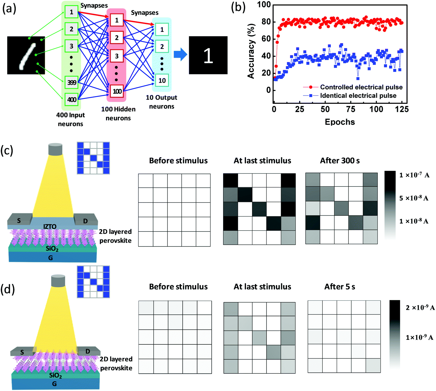 | ||
| Fig. 4 (a) Schematic illustration of multilayer neural network composed of 400 input neurons, 100 hidden neurons, and 10 output neurons. (b) The recognition accuracy of artificial neural networks based on the artificial synapses that use IZTO/2D layered OIHP device for 125 epochs under identical and controlled pulse condition. (c) Current response before stimulus, at the last stimulus, and 300 s after last stimulus by inputting the optical stimuli with image of letter of “N” consisting of 5 × 5 pixels of IZTO/2D layered OIHP optical synapses and (d) current response before stimulus, at the last stimulus, and after 5 s of 2D layered OIHP device without IZTO. | ||
Conclusions
We investigated an optical synapse that used a 2D layered OIHP (BA2PbBr4) and an amorphous oxide semiconductor (IZTO). The band alignment between IZTO and 2D layered OIHP could induce effective spatial separation of photo-excited carriers; this separation was the basis of optically-meditated charge trapping, and this trapping enabled control of conductance under illumination. The conductance increased by applying optical spikes, then returned to its initial state by applying electrical pulses. The device showed long-term potentiation and depression characteristics with a large dynamic range of ∼104, which allowed a large number of distinct synaptic states that could improve the recognition accuracy in the neuromorphic system. We confirmed the applicability of the optical synapses to ANNs by simulation of recognition accuracy. These results demonstrated the feasibility of an optical synapse based on 2D layered OIHP. We believe that this work can provide a promising route to development of neuromorphic visual systems.Author contributions
J.-S. L. conceived and directed the research. J.-S. L. and Y. P. designed and planned the experiment. Y. P. performed the experiment and acquired the data. J.-S. L., Y. P., and M.-K. K analyzed data. J.-S. L. and Y. P. wrote the manuscript.Conflicts of interest
There are no conflicts to declare.Acknowledgements
This research was supported by the Industrial Strategic Technology Development Program (20003968) funded by the Ministry of Trade, Industry & Energy (MOTIE, Korea). This research was supported by the National Research Foundation of Korea (NRF-2016M3D1A1027665 and NRF-2019R1A2C2084114) funded by Ministry of Science and ICT. In addition, this work was partially supported by the Brain Korea 21 PLUS project (Center for Creative Industrial Materials).References
- S. Gao, G. Liu, H. Yang, C. Hu, Q. Chen, G. Gong, W. Xue, X. Yi, J. Shang and R.-W. Li, ACS Nano, 2019, 13, 2634–2642 CAS.
- G. Wang, R. Wang, W. Kong and J. Zhang, Cognit. Neurodyn., 2018, 12, 615–624 CrossRef.
- W. Deng, X. Zhang, R. Jia, L. Huang, X. Zhang and J. Jie, NPG Asia Mater., 2019, 11, 77 CrossRef CAS.
- Z. D. Luo, X. Xia, M. M. Yang, N. R. Wilson, A. Gruverman and M. Alexe, ACS Nano, 2020, 14, 746–754 CrossRef CAS.
- S. Chen, Z. Lou, D. Chen and G. Shen, Adv. Mater., 2018, 30, 1705400 CrossRef.
- C. Koch and B. Mathur, IEEE Spectrum, 1996, 33, 38–46 Search PubMed.
- G. Indiveri and R. Douglas, Science, 2000, 288, 1189–1190 CrossRef.
- F. M. Ma, Y. B. Zhu, Z. W. Xu, Y. Liu, X. J. Zheng, S. Ju, Q. Q. Li, Z. Q. Ni, H. L. Hu, Y. Chai, C. X. Wu, T. W. Kim and F. S. Li, Adv. Funct. Mater., 2020, 30, 1908901 CrossRef CAS.
- H. L. Park, H. Kim, D. Lim, H. Zhou, Y. H. Kim, Y. Lee, S. Park and T. W. Lee, Adv. Mater., 2020, 32, 1906899 CrossRef CAS.
- Y. Wang, J. Yang, Z. Wang, J. Chen, Q. Yang, Z. Lv, Y. Zhou, Y. Zhai, Z. Li and S. T. Han, Small, 2019, 15, 1805431 CrossRef.
- M.-K. Kim and J.-S. Lee, Adv. Mater., 2020, 32, 1907826 CrossRef CAS.
- B. Pradhan, S. Das, J. Li, F. Chowdhury, J. Cherusseri, D. Pandey, D. Dev, A. Krishnaprasad, E. Barrios, A. Towers, A. Gesquiere, L. Tetard, T. Roy and J. Thomas, Sci. Adv., 2020, 6, eaay5225 CrossRef CAS.
- L. Yin, W. Huang, R. Xiao, W. Peng, Y. Zhu, Y. Zhang, X. Pi and D. Yang, Nano Lett., 2020, 20, 3378–3387 CrossRef CAS.
- K. Wang, S. Dai, Y. Zhao, Y. Wang, C. Liu and J. Huang, Small, 2019, 15, 1900010 CrossRef.
- L. Qian, Y. Sun, M. Wu, C. Li, D. Xie, L. Ding and G. Shi, Nanoscale, 2018, 10, 6837–6843 RSC.
- X. Zhu and W. D. Lu, ACS Nano, 2018, 12, 1242–1249 CrossRef CAS.
- S. Ham, S. Choi, H. Cho, S.-I. Na and G. Wang, Adv. Funct. Mater., 2019, 29, 1806646 CrossRef.
- Y. Wang, Z. Lv, J. Chen, Z. Wang, Y. Zhou, L. Zhou, X. Chen and S. T. Han, Adv. Mater., 2018, 30, 1802883 CrossRef.
- Q. Wang, B. Chen, Y. Liu, Y. Deng, Y. Bai, Q. Dong and J. Huang, Energy Environ. Sci., 2017, 10, 516–522 RSC.
- B. Li, Y. Li, C. Zheng, D. Gao and W. Huang, RSC Adv., 2016, 6, 38079–38091 RSC.
- B. Hwang and J.-S. Lee, Adv. Opt. Mater., 2019, 7, 1801356 CrossRef.
- H. Lin, C. Zhou, Y. Tian, T. Siegrist and B. Ma, ACS Energy Lett., 2018, 3, 54–62 CrossRef CAS.
- S. Chen and G. Shi, Adv. Mater., 2017, 29, 1605448 CrossRef.
- K. Hong, Q. V. Le, S. Y. Kim and H. W. Jang, J. Mater. Chem. C, 2018, 6, 2189–2209 RSC.
- Y. Liao, H. Liu, W. Zhou, D. Yang, Y. Shang, Z. Shi, B. Li, X. Jiang, L. Zhang, L. N. Quan, R. Quintero-Bermudez, B. R. Sutherland, Q. Mi, E. H. Sargent and Z. Ning, J. Am. Chem. Soc., 2017, 139, 6693–6699 CrossRef CAS.
- J. Zhou, Y. Chu and J. Huang, ACS Appl. Mater. Interfaces, 2016, 8, 25660–25666 CrossRef CAS.
- F. Li, C. Ma, H. Wang, W. Hu, W. Yu, A. D. Sheikh and T. Wu, Nat. Commun., 2015, 6, 8238 CrossRef.
- S. Chen, C. Teng, M. Zhang, Y. Li, D. Xie and G. Shi, Adv. Mater., 2016, 28, 5969–5974 CrossRef CAS.
- J.-Y. Chen, Y.-C. Chiu, Y.-T. Li, C.-C. Chueh and W.-C. Chen, Adv. Mater., 2017, 29, 1702217 CrossRef.
- S. Yu, Proc. IEEE, 2018, 106, 260–285 CAS.
- A. Melianas, T. J. Quill, G. LeCroy, Y. Tuchman, H. V. Loo, S. T. Keene, A. Giovannitti, H. R. Lee, I. P. Maria, I. McCulloch and A. Salleo, Sci. Adv., 2020, 6, eabb2958 CrossRef CAS.
- X. W. Feng, X. K. Liu and K. W. Ang, Nanophotonics, 2020, 9, 1579–1599 CAS.
- D. Lee, B. Hwang and J.-S. Lee, ACS Appl. Mater. Interfaces, 2019, 11, 20225–20231 CrossRef CAS.
- B. Hwang and J.-S. Lee, Adv. Mater., 2017, 29, 1701048 CrossRef.
- L. K. Ono, M. R. Leyden, S. Wang and Y. Qi, J. Mater. Chem. A, 2016, 4, 6693–6713 RSC.
- A. Biswas, R. Bakthavatsalam and J. Kundu, Chem. Mater., 2017, 29, 7816–7825 CrossRef CAS.
- R. Azmi, N. Nurrosyid, S.-H. Lee, M. Al Mubarok, W. Lee, S. Hwang, W. Yin, T. K. Ahn, T.-W. Kim, D. Y. Ryu, Y. R. Do and S.-Y. Jang, ACS Energy Lett., 2020, 5, 1396–1403 CrossRef CAS.
- Z. Yu, Z. Yang, Z. Ni, Y. Shao, B. Chen, Y. Lin, H. Wei, Z. J. Yu, Z. Holman and J. Huang, Nat. Energy, 2020, 5, 657–665 CrossRef CAS.
- Z. Ni, C. Bao, Y. Liu, Q. Jiang, W.-Q. Wu, S. Chen, X. Dai, B. Chen, B. Hartweg, Z. Yu, Z. Holman and J. Huang, Science, 2020, 367, 1352–1358 CrossRef CAS.
- Y. Chen, N. Li, L. Wang, L. Li, Z. Xu, H. Jiao, P. Liu, C. Zhu, H. Zai, M. Sun, W. Zou, S. Zhang, G. Xing, X. Liu, J. Wang, D. Li, B. Huang, Q. Chen and H. Zhou, Nat. Commun., 2019, 10, 1112 CrossRef.
- A. Fakharuddin, W. Qiu, G. Croes, A. Devižis, R. Gegevičius, A. Vakhnin, C. Rolin, J. Genoe, R. Gehlhaar, A. Kadashchuk, V. Gulbinas and P. Heremans, Adv. Funct. Mater., 2019, 29, 1904101 CrossRef.
- N. Liu, P. Liu, H. Zhou, Y. Bai and Q. Chen, J. Phys. Chem. Lett., 2020, 11, 3521–3528 CrossRef CAS.
- J. Haruyama, K. Sodeyama, L. Han and Y. Tateyama, J. Am. Chem. Soc., 2015, 137, 10048–10051 CrossRef CAS.
- S. Meloni, T. Moehl, W. Tress, M. Franckevičius, M. Saliba, Y. H. Lee, P. Gao, M. K. Nazeeruddin, S. M. Zakeeruddin, U. Rothlisberger and M. Graetzel, Nat. Commun., 2016, 7, 10334 CrossRef CAS.
- B. Hwang, C. Gu, D. Lee and J.-S. Lee, Sci. Rep., 2017, 7, 43794 CrossRef.
- Y. Lin, Y. Bai, Y. Fang, Q. Wang, Y. Deng and J. Huang, ACS Energy Lett., 2017, 2, 1571–1572 CrossRef CAS.
- X. Xiao, J. Dai, Y. Fang, J. Zhao, X. Zheng, S. Tang, P. N. Rudd, X. C. Zeng and J. Huang, ACS Energy Lett., 2018, 3, 684–688 CrossRef CAS.
- W. Xu, H. Cho, Y. H. Kim, Y. T. Kim, C. Wolf, C. G. Park and T. W. Lee, Adv. Mater., 2016, 28, 5916–5922 CrossRef CAS.
- B. Chen, M. Yang, S. Priya and K. Zhu, J. Phys. Chem. Lett., 2016, 7, 905–917 CrossRef CAS.
- S. Wei, F. Wang, X. Zou, L. Wang, C. Liu, X. Liu, W. Hu, Z. Fan, J. C. Ho and L. Liao, Adv. Mater., 2020, 32, 1907527 CrossRef CAS.
- C. Xie and F. Yan, J. Mater. Chem. C, 2018, 6, 1338–1342 RSC.
- C. Xie, P. You, Z. Liu, L. Li and F. Yan, Light: Sci. Appl., 2017, 6, e17023 CrossRef.
- Y. Liu, H. Wei, J. Guo, P.-A. Chen, S. Liu, J. Li, L. Miao, N. Wang, Z. Chen, J. Wang, H. Chen and Y. Hu, Org. Electron., 2019, 75, 105372 CrossRef CAS.
- E. R. Kandel, Science, 2001, 294, 1030–1038 CrossRef CAS.
- S. J. Martin, P. D. Grimwood and R. G. M. Morris, Annu. Rev. Neurosci., 2000, 23, 649–711 CrossRef CAS.
- L. F. Abbott and S. B. Nelson, Nat. Neurosci., 2000, 3, 1178–1183 CrossRef CAS.
- J. L. McGaugh, Science, 2000, 287, 248–251 CrossRef CAS.
- T. Ohno, T. Hasegawa, T. Tsuruoka, K. Terabe, J. K. Gimzewski and M. Aono, Nat. Mater., 2011, 10, 591–595 CrossRef CAS.
- R. S. Zucker and W. G. Regehr, Annu. Rev. Physiol., 2002, 64, 355–405 CrossRef CAS.
- Y. H. Liu, L. Q. Zhu, P. Feng, Y. Shi and Q. Wan, Adv. Mater., 2015, 27, 5599–5604 CrossRef CAS.
- C. S. Yang, D. S. Shang, N. Liu, G. Shi, X. Shen, R. C. Yu, Y. Q. Li and Y. Sun, Adv. Mater., 2017, 29, 1700906 CrossRef.
- L. Yin, C. Han, Q. Zhang, Z. Ni, S. Zhao, K. Wang, D. Li, M. Xu, H. Wu, X. Pi and D. Yang, Nano Energy, 2019, 63, 103859 CrossRef CAS.
- Y. Sun, L. Qian, D. Xie, Y. Lin, M. Sun, W. Li, L. Ding, T. Ren and T. Palacios, Adv. Funct. Mater., 2019, 29, 1902538 CrossRef.
- S. Choi, S. H. Tan, Z. Li, Y. Kim, C. Choi, P. Y. Chen, H. Yeon, S. Yu and J. Kim, Nat. Mater., 2018, 17, 335–340 CrossRef CAS.
- S. Ambrogio, P. Narayanan, H. Tsai, R. M. Shelby, I. Boybat, C. di Nolfo, S. Sidler, M. Giordano, M. Bodini, N. C. P. Farinha, B. Killeen, C. Cheng, Y. Jaoudi and G. W. Burr, Nature, 2018, 558, 60–67 CrossRef CAS.
- M. K. Kim and J.-S. Lee, Nano Lett., 2019, 19, 2044–2050 CrossRef CAS.
Footnote |
| † Electronic supplementary information (ESI) available. See DOI: 10.1039/d0tc04250a |
| This journal is © The Royal Society of Chemistry 2021 |