
 Open Access Article
 This Open Access Article is licensed under a Creative Commons Attribution-Non Commercial 3.0 Unported Licence
Isotopic study of Raman active phonon modes in β-Ga2O3†
Benjamin M.
Janzen
 a,
Piero
Mazzolini
bc,
Roland
Gillen
d,
Andreas
Falkenstein
e,
Manfred
Martin
e,
Hans
Tornatzky
af,
Janina
Maultzsch
d,
Oliver
Bierwagen
b and
Markus R.
Wagner
*a
a,
Piero
Mazzolini
bc,
Roland
Gillen
d,
Andreas
Falkenstein
e,
Manfred
Martin
e,
Hans
Tornatzky
af,
Janina
Maultzsch
d,
Oliver
Bierwagen
b and
Markus R.
Wagner
*a
aTechnische Universität Berlin, Institute of Solid State Physics, Hardenbergstr. 36, 10623 Berlin, Germany. E-mail: markus.wagner@physik.tu-berlin.de
bPaul-Drude-Institut für Festkörperelektronik, Leibniz-Institut im Forschungsverbund Berlin e.V., Hausvogteiplatz 5-7, 10117 Berlin, Germany
cDepartment of Mathematical, Physical and Computer Sciences, University of Parma, Viale delle Scienze 7/A, 43124 Parma, Italy
dChair of Experimental Physics, Friedrich-Alexander Universität Erlangen-Nürnberg, Staudtstr. 7, 91058 Erlangen, Germany
eInstitute of Physical Chemistry, RWTH Aachen University, Landoltweg 2, 52074 Aachen, Germany
fUniversité de Toulouse, INSA-CNRS-UPS, LPCNO, 135 avenue de Rangueil, 31077 Toulouse, France
First published on 11th January 2021
Abstract
Holding promising applications in power electronics, the ultra-wide band gap material gallium oxide has emerged as a vital alternative to materials like GaN and SiC. The detailed study of phonon modes in β-Ga2O3 provides insights into fundamental material properties such as crystal structure and orientation and can contribute to the identification of dopants and point defects. We investigate the Raman active phonon modes of β-Ga2O3 in two different oxygen isotope compositions (16O,18O) by experiment and theory: By carrying out polarized micro-Raman spectroscopy measurements on the (010) and (![[2 with combining macron]](https://www.rsc.org/images/entities/char_0032_0304.gif) 01) planes, we determine the frequencies of all 15 Raman active phonons for both isotopologues. The measured frequencies are compared with the results of density functional perturbation theory (DFPT) calculations. In both cases, we observe a shift of Raman frequencies towards lower energies upon substitution of 16O with 18O. By quantifying the relative frequency shifts of the individual Raman modes, we identify the atomistic origin of all modes (Ga–Ga, Ga–O or O–O) and present the first experimental confirmation of the theoretically calculated energy contributions of O lattice sites to Raman modes. The DFPT results enable the identification of Raman modes that are dominated by the different, inequivalent O- or Ga-atoms of the unit cell. We find that oxygen substitution on the OIII site leads to an elevated relative mode frequency shift compared to OI and OII sites. This study presents a blueprint for the future identification of different point defects in Ga2O3 by Raman spectroscopy.
01) planes, we determine the frequencies of all 15 Raman active phonons for both isotopologues. The measured frequencies are compared with the results of density functional perturbation theory (DFPT) calculations. In both cases, we observe a shift of Raman frequencies towards lower energies upon substitution of 16O with 18O. By quantifying the relative frequency shifts of the individual Raman modes, we identify the atomistic origin of all modes (Ga–Ga, Ga–O or O–O) and present the first experimental confirmation of the theoretically calculated energy contributions of O lattice sites to Raman modes. The DFPT results enable the identification of Raman modes that are dominated by the different, inequivalent O- or Ga-atoms of the unit cell. We find that oxygen substitution on the OIII site leads to an elevated relative mode frequency shift compared to OI and OII sites. This study presents a blueprint for the future identification of different point defects in Ga2O3 by Raman spectroscopy.
1 Introduction
Gallium oxide (Ga2O3) is a semiconductor material with an ultra-wide bandgap of about 4.8 eV,1,2 enabling applications in power-electronics devices such as rectifiers,3,4 metal-semiconductor field-effect transistors (MESFETs),5,6 metal oxide semiconductor field-effect transistors (MOSFETs)3,4,7 or deep-UV photodetectors.8,9 The material may, depending upon temperature and pressure, exist in five different polymorphs: α, β, γ, κ (mostly referred as ε)10 and δ.3,11–19 The majority of the Ga2O3 related research focuses on the β-phase as it is the thermodynamically most stable phase11,12,18 and can be produced as bulk single crystals by different growth techniques such as the Czochralski method,20–23 floating-zone,1,24–27 edge-defined film fed (EFG),23,28 or Bridgman (horizontal or vertical, HB and VB)29–31 growth methods.1.1 Crystal structure and electronic properties
The crystal structure of the β-polymorph (Fig. 1) is monoclinic (space group: C32h; C2/m)12,19,32 with lattice parameters a = 12.29 Å, b = 3.05 Å, c = 5.81 Å and the monoclinic angle of β = 103.77° between the crystallographic a and c axes.19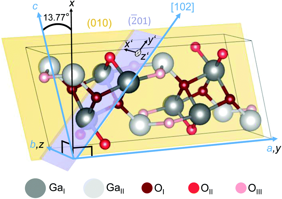 | ||
| Fig. 1 Unit cell of monoclinic β-Ga2O3. Two types of Ga (GaI and GaII) and three types of O (OI, OII and OIII) lattice sites are illustrated. By aligning the y and z axes of a Cartesian coordinate system (black) along the crystallographic a and b axes (blue), the x and c axes confine an angle of 13.77°.19 The (010) plane (yellow) is spanned by the a and c axes. Cartesian coordinates x′||b and y′||[102] parameterize the (01) plane (violet), with z′ denoting the surface normal. The crystallographic plot was created using VESTA.57 | ||
The commercial availability of β-Ga2O3 substrates with different surface planes enables lattice-matched strain-free homoepitaxial growth of β-Ga2O3 films with low defect densities.33–40 Nonetheless, even in the case of homoepitaxy, different substrate orientations can result in the formation of structural defects in the deposited layers, e.g. twin domains in (100) and (01) films.33,38 In order to overcome this problem, homoepitaxial growth of β-Ga2O3 is mostly performed on (010) oriented substrates,34 although viable alternatives such as (001) homoepitaxy33 or the employment of proper offcuts in (100) oriented substrates41 were recently reported.
Previous works have demonstrated the possibility of extrinsic n-doping by substituting Ga atoms with electron donors like Si,42 Sn,43 Ge44 and Nb.45 To date, the reported charge carrier densities in β-Ga2O3 bulk crystals46,47 and thin films44,45,48 have rarely exceeded high 1019 cm−3. Free carrier concentrations are commonly limited by point defects and structural defects. Theoretical works49–56 have addressed the effects of Ga and O point defects in gallium oxide on the electrical and optical properties. Using hybrid functional calculations, it was revealed that oxygen vacancies (VO) are deep donors with ionization energies above 1 eV and hence do not contribute to the observed n-type conductivity in unintentionally doped β-Ga2O3.49 Succeeding studies found that all other native defects, except for gallium interstitials (Gai), are deep, too.53–55 While Gai may act as shallow donors, their high mobility, coupled with large formation energies under n-type conditions inhibit their contribution to the electrical conductivity.56
Whereas intrinsic defects should not be the main source of electrical conductivity, different impurities including H, Si, Ge, Sn, F and Cl could act as extrinsic shallow donors.49,50 Moreover, a large concentration of point defects can also affect the mobility of free charge carriers. Nonetheless, from an experimental point of view both (i) the control over the formation of different point defects during the material synthesis and (ii) their unambiguous identification is extremely difficult to achieve, but potentially of paramount importance for fully exploiting the material potential. In order to address this challenge, we conduct a combined experimental and theoretical study of the impact of different lattice atoms on phonon modes in β-Ga2O3 isotopologues.
1.2 Lattice dynamics
Polarized micro-Raman spectroscopy constitutes a powerful tool that enables e.g. the study of strain in epitaxial thin films,58 the detection of dopants and point defects via local vibrational modes,59 the identification of lattice sites via angular resolved measurements,60 and the determination of the thermal conductivity via Raman thermometry in its one and two laser implementations.61,62 Symmetries and spectral positions of Raman active phonons of β-Ga2O3 in the natural 16O isotopic composition have been calculated theoretically and verified experimentally in a number of publications.60,63–66 Two recent works60,66 employed polarized micro-Raman spectroscopy to separate Raman modes of different symmetries. Infrared active phonons were investigated by IR ellipsometry.67 The influence of lattice expansion was studied by temperature dependent Raman spectroscopy of β-Ga2O3.63 Employing the valence force field calculation, the authors indentified three categories of Raman active phonons with respect to the motions of Ga and O atoms. The transition of the β- to the α-phase under high pressure was investigated by carrying out Raman spectroscopy in diamond anvil cells.64 Raman tensor elements were determined in angular-resolved measurements60 using a modified Raman tensor formalism proposed in a preceding publication.68 Though the effects of isotope substitution on the frequencies of the Raman active phonon modes in β-Ga2O3 were investigated theoretically,69 no corresponding experimental study is available in the literature.Raman vibrations may be excited by oscillations of Ga or O atoms. By calculating the displacements of the individual O or Ga lattice sites, density functional perturbation theory (DFPT) calculations enable the identification of the atomistic origins of vibrational modes (Ga–Ga, Ga–O or O–O). From an experimental point of view, the identification of individual lattice sites in materials with large unit cells is a challenging endeavour. A powerful tool is the usage of different isotopes and investigate their impact on the vibrational properties of a material. This approach was successfully applied in TiO2 enabling the experimental identification of Raman modes without any contribution of oxygen lattice vibrations as evidenced by the unchanged frequency of the Eg(1) and B1g(1) modes in anatase TiO2.70,71
Alternatively, the introduction of different isotopes of the same dopant can provide an unambiguous identification of dopant related local vibrational modes. ZnO is a well-studied wide band-gap oxide, whose point defects have been thoroughly investigated by vibrational spectroscopy. Apart from Zn and O vacancies, point defects in ZnO include Zn on interstitial sites (Zni) and oxygen on interstitial sites (Oi).72,73 Undoped ZnO exhibits intrinsic n-type conductivity, which is commonly attributed to one or more of the following origins: (i) intrinsic defects acting as shallow donors,74,75 (ii) shallow donors due to H absorbed from the air,76–79 (iii) shallow donors formed by residual trace amounts of group – III impurities such as Al, Ga and In.80 The substitution of N on O lattice sites in ZnO produced a pair of additional modes at ν ≈ 274 and 510 cm−1,81–84 irrespective of the implanted N isotope.85,86 Moreover, since the doping of ZnO with Ga, Fe, Sb, Li and Al yielded the same vibrational modes,87 their occurrence was tentatively attributed to a Zni–Ni or Zni–Oi complex.83 By investigating undoped and nitrogen-doped ZnO thin films in different Zn isotope compositions, the presence of the 274 cm−1 mode was eventually revealed to be related to interstitial Zn clusters depending on the surface polarity of ZnO.84 This experimental approach could represent an important milestone for the future identification of different point defects in Ga2O3 layers as a function of different synthesis (e.g. deposition, annealing) conditions.88 Oxygen defects such as O-vacancies and nitrogen on O-sites are deep donors and acceptors, respectively, which can strongly impact electronic behavior (traps, scattering centers, centers that get charged/discharged in space-charge devices). These defects need to be studied and we propose on the long run to use Raman spectroscopy for it.
Towards this goal, this work investigates the phonon frequencies of β-Ga2O3 in the natural 16O and 18O isotope compositions using confocal and cross-sectional micro-Raman spectroscopy. The acquired experimental data are complemented with the results of DFPT calculations. By quantifying the relative frequency shifts of the individual Raman modes, we discuss the origins of vibration dynamics (Ga–Ga, Ga–O or O–O), resolved for different non-equivalent lattice sites, and present the first experimental confirmation of the theoretically calculated energy contribution of O sites to Raman modes. The results of our study shall open the possibility of analyzing O-related point defects in β-Ga2O3 by Raman spectroscopy.
2 Experimental and theoretical methods
A β-Ga2O3 layer was homoepitaxially deposited (deposition time 445 min) on top of an unintentionally doped (010)-oriented substrate with In-mediated metal-exchange catalysis (MEXCAT)89–91 in an MBE chamber equipped with an oxygen-plasma source run at a power of 300 W. For this deposition run, nominally 97.39% isotopically enriched 18O2 was employed to provide an oxygen flux of 0.38 standard cubic centimeter per minute (sccm) during the layer growth. For gallium (with natural isotopic abundance) a beam equivalent pressure (BEP) of BEPGa = 1.27 × 10⁻⁷ mbar was used (equivalent to a particle flux of ΦGa = 2.2 nm−2 s−1), while the additional In-flux necessary to allow the catalytic growth of the layer at a substrate temperature of Tg = 900 °C was set to ΦIn = 1/3 ΦGa (BEPIn = 5.2 × 10⁻⁸ mbar).The 18O isotope fraction, n*, within the sample was determined by time-of-flight secondary ion mass spectrometry (ToF-SIMS) depth profiles on a ToF-SIMS IV machine (IONTOF GmbH, Münster, Germany). Measurements were performed with a 25 kV Ga+ analysis beam and a 2 kV Cs+ sputter beam. The isotope fraction is directly accessible from the 18O and 16O intensities by
 | (1) |
Crater depths were analysed by interference microscopy with a WYKO NT1100 (Veeco Instruments Inc., USA).
Raman scattering at room temperature (293 K) was excited by a 632.816 nm He–Ne laser on a LabRAM HR 800 spectrometer (Horiba Jobin-Yvon, France). The laser beam was focused onto the sample using a 100× Olympus objective with a numerical aperture (NA) of 0.9, with the scattered light being collected in backscattering geometry. Backreflected and elastically scattered light (Rayleigh component) was filtered using an ultra low frequency filter (ULF) unit and then spectrally-dispersed by a monochromator spectrometer with a grating of 1800 lines per mm. The light was detected by a charge-coupled device (CCD). The spectral dispersion of the setup is 0.35 cm−1 per pixel. The spectral resolution at 650 nm (400 cm−1) using the 1800 lines per mm grating is about 0.5 cm−1. The precision in the determination of peak positions in comparison to neighboring Raman modes after line shape fitting for non-overlapping modes is better than 0.1 cm−1. The sample was placed beneath the objective with a respective surface's normal parallel to the direction of light propagation. A λ/2 wave plate in the excitation was set at 0° or 45° to polarize the incident light parallel or crossed with respect to the scattered light, which was selected using a fixed polarizer in the detection. Prior to each measurement, the Raman spectrometer was calibrated using the silicon T2g-peak at 520.7 cm−1.
Simulations of the lattice vibrations were performed within the frame of density functional perturbation theory (DFPT) on the level of the local density approximation (LDA) as implemented into the Quantum Espresso suite.92 The Ga(3s,3p,3d) and the O(2s,2p) states were treated as valence electrons using multi-projector optimized normconserving Vanderbildt (ONCV) pseudopotentials93 from the Pseudo Dojo repository,94 where we used a large cutoff of the planewave basis set of 180 Ry. All reciprocal space integrations were performed by a discrete k-point sampling of 7 × 7 × 7 points in the Brillouin zone. We fully optimized the atomic positions and cell parameters of the primitive cell of β-Ga2O3 until the residual forces between atoms and the cell stress were smaller than 0.0025 eV Å−1 and 0.01 GPa, respectively. The threshold for the total energy was set to 10−15 Ry, which ensured tightly converged interatomic forces for the geometry optimization and of the ground state density and wavefunctions for the DFPT calculations. As a result of the intrinsic underbinding of the LDA exchange–correlation functional, our optimized lattice constants are less than 1% underestimated compared to the experimental values (Table 1). On the other hand, it is well-known that the LDA overbinding gives rise to a typically very good agreement of the DFT phonon frequencies,95 motivating our choice for the purposes of this work.
3 Results and discussion
The Raman-active phonon modes of β-Ga2O3 in the 16O and 18O isotoplogues (substrate and film, respectively) were acquired in polarized micro-Raman measurements, the results of which are depicted in Fig. 2a–c. From ToF-SIMS experiments, the dominating presence of 18O in the homoepitaxial film has been verified: the isotope fraction is 96.3% and remains constant up to a depth of 1.5 μm from the surface (Fig. S2 in ESI†). At the interface between film and substrate, the isotope fraction drops over an intermediate region of 300 nm to 0.3%, which is slightly higher than the natural isotope abundance of 0.2%. The difference might be caused by diffusion during the deposition process at elevated temperatures. The depth with 50% of the initial isotope fraction marks the interface of the film resulting in a film thickness of 1.65 μm (AFM micrography of the layer reported in Fig. S1 of ESI†). | ||
| Fig. 2 Raman spectra of the homoepitaxially-grown Ga2O3 thin film (18O) on the (010) plane of a β-Ga2O3 substrate with natural (16O) isotope abundance. (a and b) Raman spectra in parallel polarization for excitation on the (010)-plane. Substrate spectra (dark yellow) were subtracted from the epilayer spectra (blue) to obtain difference spectra (green), in which 18O Raman modes (denoted by *) dominate. For clarity, spectra are vertically offset and the difference spectra multiplied by a constant factor. The Cartesian coordinate system x, y, z is chosen such that z-axis aligns with the [010] direction, while y||[100]. (c) Raman spectra of the (01)-plane in crossed polarization. The z′-axis is parallel to the surface normal, with x′||[010] and y′||[102]. (d) Schematic illustration of sample set-up, plane orientation, and measurement geometry. The (010) plane was accessible in confocal micro-Raman scattering (left). The [102] direction is oriented along an edge of the square-shaped wafer. Spectra of the (01)-plane were acquired by focusing the laser on the edge of the sample in cross-section geometry (right). | ||
The MEXCAT deposition process33,91,98 allows to widen the deposition window of Ga2O3 to otherwise forbidden growth regimes (e.g. the high Tg and metal-to-oxygen flux ratios used in this work), while at the same time allowing for low incorporation of the catalyzing element.
The primitive unit cell of the monoclinic structure consists of 10 atoms: Ga lattice sites occur in tetrahedral (GaI) or octahedral (GaII) coordination, with three nonequivalent oxygen sites (OI, OII and OIII) in between. At the Γ-point, these correspond to 27 optical phonons:60,63,66
| Γopt = 10Ag + 5Bg + 4Au + 8Bu, | (2) |
All 15 Raman-active phonon modes of symmetries Ag and Bg were separated by utilization of the measurement geometries illustrated in Fig. 2d. The sample was irradiated normally in a confocal setup (left) and on the edge (right) to access the (010) or (01) plane, respectively. The choice of the (010) and (01) planes is advantageous as it enables the selected detection of Raman modes with Ag or Bg symmetry and thus facilitates the separation of modes with closely matching phonon frequencies. For the (010) plane, Bg-modes are forbidden as determined by Raman selection rules. For excitation normal to the (01)-plane, Ag modes have vanishing intensity for crossed polarization of incident and scattered light when the polarization of the incident radiation aligns with the [010] direction.60,63
Fig. 2a illustrates the Raman spectra of the (010) plane in parallel polarization between incident and scattered light. Using the Porto notation, the applied scattering geometry can be written as z(yy)![[z with combining macron]](https://www.rsc.org/images/entities/i_char_007a_0304.gif) , where z and y correspond to the [010] and [100] directions, respectively (cf.Fig. 1).60,63,66 In this configuration, the A1g, A2g, A3g, A7g and A8g modes have maximum intensity. As we only investigated phonon modes accessible in Raman measurements, the index g denoting a Raman-active mode is omitted in the following discussion. The Raman spectra of the substrate with 16O (dark yellow) and the epilayer with 18O (blue) were recorded in a confocal set-up by moving the z-focus into the substrate (minimum signal contribution from the film) and into the film (maximum film contribution). By subtracting the two spectra from each other, we obtained a difference spectrum (green), in which the 18O Raman modes dominate. For clarity spectra are vertically offset and the difference spectrum is scaled by a constant factor. 18O Raman modes are labeled with * to distinguish them from 16O modes.
, where z and y correspond to the [010] and [100] directions, respectively (cf.Fig. 1).60,63,66 In this configuration, the A1g, A2g, A3g, A7g and A8g modes have maximum intensity. As we only investigated phonon modes accessible in Raman measurements, the index g denoting a Raman-active mode is omitted in the following discussion. The Raman spectra of the substrate with 16O (dark yellow) and the epilayer with 18O (blue) were recorded in a confocal set-up by moving the z-focus into the substrate (minimum signal contribution from the film) and into the film (maximum film contribution). By subtracting the two spectra from each other, we obtained a difference spectrum (green), in which the 18O Raman modes dominate. For clarity spectra are vertically offset and the difference spectrum is scaled by a constant factor. 18O Raman modes are labeled with * to distinguish them from 16O modes.
Subsequently, the polarization vectors of both the incident and scattered radiation were rotated 90° around the [010] direction. The x-axis and the [001] direction confined an angle of 13.77° (Fig. 1), yielding the configuration z(xx), in which the A5, A6, A9 and A10 modes are maximal. The same procedures as above were applied to acquire the substrate, epilayer and difference spectra, which are displayed in Fig. 2b. The objective's large NA (0.9) implies a relaxation of selection rules, as light is also collected from directions other than perpendicular to the (010) plane. Hence, the most-intense B2-mode is weakly present in Fig. 2b.
To access the B-modes, Raman scattering was performed in a cross-section configuration. The thickness of the film equals approximately twice the diffraction limited extent of the laser of about 800 nm. In order to obtain the Raman spectrum of the homoepitaxial layer, we performed cross-section line scans with 200 nm step size. Based on these linescans, we selected two positions for long integration Raman measurements, one for which the 18O related Raman modes reach maximum intensity and a second one for which only substrate modes are visible. Subtracting of the resulting spectra yielded the difference spectrum (green) in Fig. 2c.
The in-plane crystalline directions of the (010)-oriented sample were identified (i) by the presence of a rounded edge in the used substrate correspondent to the [102] crystalline direction (orthogonal to the (01) planes, cf.Fig. 2d), (ii) by X-ray diffraction (XRD) 2θ- and φ-scans performed on different (010) crystals, and (iii) by the recognition of (110)-facets visible as oriented lines along the [001] in-plane orientation in AFM micrographs (cf. Fig. S1b, ESI†).91,98 Indeed the correct probe of the (01) planes was experimentally verified via Raman spectroscopy which highlighted the mode intensity ratios expected for the (01) planes (Fig. 2c)60. We thus selected an edge, whose surface plane corresponds to the (01) plane. For normal incidence z′ (cf.Fig. 1) with crossed polarization in the z′(x′y′)′ configuration (x′||[010], y′||[102]), Raman selection rules predict vanishing intensity for the A modes and maximum intensity for the B modes. Due to the edge's imperfect preparation, A-modes were still present, yet less intense. An intensity ratio of about 3![[thin space (1/6-em)]](https://www.rsc.org/images/entities/char_2009.gif) :1 between the most intense B2 and A3 modes was achieved. All five B-modes are hence available in this configuration.
:1 between the most intense B2 and A3 modes was achieved. All five B-modes are hence available in this configuration.
The spectral positions of 16O and 18O Raman modes are derived from the difference spectra in Fig. 2a–c by fitting Lorentzian lineshape functions. The obtained peak positions are listed in Table 2 for both O isotopes in conjunction with the results of DFPT calculations. A few modes deserve particular attention, as the determination of their spectral positions and relative frequency shifts is challenging due to small frequency shifts or overlapping modes. This applies to the low-frequency A1, B1, B2 and A2 modes, for which the frequency shifts are in the order of the respective mode's linewidth.
| Phonon mode | Experiment | Theory | ||||||
|---|---|---|---|---|---|---|---|---|
| 16O (cm−1) | 18O (cm−1) | Absolute shift (cm−1) | Relative shift (cm−1) | 16O (cm−1) | 18O (cm−1) | Absolute shift (cm−1) | Relative shift (cm−1) | |
| A1g | 110.7 | 110.2 | 0.5 | 0.43 | 106.4 | 105.7 | 0.7 | 0.62 |
| B1g | 114.3 | 113.5 | 0.8 | 0.68 | 107.7 | 106.7 | 1.0 | 0.91 |
| B2g | 144.9 | 143.4 | 1.5 | 1.03 | 145.0 | 144.0 | 1.0 | 0.71 |
| A2g | 169.8 | 168.7 | 1.1 | 0.62 | 163.1 | 161.8 | 1.3 | 0.79 |
| A3g | 200.3 | 193.7 | 6.6 | 3.32 | 190.5 | 183.6 | 6.9 | 3.62 |
| A4g | 320.3 | 315.4 | 4.9 | 1.54 | 314.0 | 308.1 | 5.9 | 1.87 |
| A5g | 347.0 | 337.5 | 9.5 | 2.74 | 345.0 | 336.0 | 9.0 | 2.60 |
| B3g | 353.4 | 334.1 | 19.3 | 5.47 | 351.4 | 331.4 | 20.0 | 5.69 |
| A6g | 416.7 | 399.0 | 17.7 | 4.24 | 384.2 | 368.3 | 15.9 | 4.14 |
| A7g | 475.3 | 453.3 | 22.0 | 4.63 | 458.9 | 435.5 | 23.4 | 5.11 |
| B4g | 475.9 | 453.6 | 22.3 | 4.70 | 473.3 | 449.3 | 24.0 | 5.07 |
| A8g | 630.4 | 599.6 | 30.8 | 4.87 | 620.3 | 589.1 | 31.2 | 5.04 |
| B5g | 652.4 | 621.3 | 31.1 | 4.76 | 644.4 | 613.1 | 31.3 | 4.86 |
| A9g | 659.0 | 627.2 | 31.8 | 4.83 | 648.5 | 614.8 | 33.7 | 5.20 |
| A10g | 767.3 | 727.7 | 39.6 | 5.16 | 751.5 | 709.6 | 41.9 | 5.58 |
Furthermore, in the Raman spectra of the substrate (dark yellow) shown in Fig. 2c, the B3 resides in the right shoulder of the A5. As for the 18O distribution (green), the two modes are superimposed in a joint widened peak. With the  position derived from Fig. 2b, we analysed this peak by setting the position of the
  fixed and varying the position of the
  until the intensity ratio
  was equal to the intensity ratio A5/B3. In the 16O substrate spectrum the B5 is closely neighbored by the A9. The
  envelope in the 18O difference spectrum is composed of three individual modes: In addition to the
  , the
, the  as well as the A8 mode from the substrate lie in close proximity. The intensity of the A8 can be regarded as negligible due to its suppression in the difference spectrum. In analogy to the analysis of the
  spectral position, the
  Raman frequency is obtained by setting the
  position determined from the difference spectrum in Fig. 2b fixed and varying the
  position until obtaining equal intensity ratios for
  and A9/B5.
Distinguishing the A7 and B4 modes in both isotope compositions is a formidable task in the literature, as the two modes are located at nearly the same frequency. With the exception of one publication,66 previous experimental works have usually reported both modes at the same frequency or have only assigned one mode,60,63,64 whereas theoretical works have calculated a frequency difference ranging from 0.3 to 13.4 cm−1 between these two modes.60,63–65
Using a (01)-oriented β-Ga2O3 sample as reference, we obtained an intensity ratio B4/B2 > 1/28 between the B4 and B2 mode in the z′(x′y′)′ configuration. Using this intensity ratio, we conclude that the B4 and  will contribute more than 70% to the total intensity of the occurring peaks at 475.9 cm−1 and 453.6 cm−1. Hence, we assign these peaks to the B4 and
  , respectively. Analogously, the peak positions of the A7 and
  are determined from the analysis of the (010) spectra in Fig. 2a with a negligible B4 or
  intensity, respectively. Consequently, we obtain a previously unresolved mode spacing of the A7 and B4 of 0.6 cm−1 and 0.3 cm−1 for the 16O and 18O isotopologues.
Following this detailed analysis, we were able to determine the spectral positions of all 15 Raman-active phonon modes in the 16O and 18O isotopologues of β-Ga2O3 (summarized in Table 2).
While a slight change in the oxygen mass does not affect the formation of point defects during the MBE growth, altering the mass of one of the two elements of a binary oxide induces a shift in Raman modes, in which atomic vibrations of the respective element are present. Owing to the larger relative mass difference between e.g.16O and 18O compared to stable Ga isotopes, oxygen isotopes produce an elevated frequency shift and are preferably used to study the variation of phonon frequencies in different isotopologues.99 The observed shift of Raman modes towards lower frequencies upon substitution of 16O with 18O corresponds to an increase in the isotopic mass.99,100
Table 2 further lists the absolute and relative frequency shift for each mode. Based on the data displayed in Table 2, Fig. 3a depicts the experimentally- (blue) and theoretically-determined (green) relative mode frequency shifts for all 15 Raman active modes. Errors in the experimental data originate from the uncertainties in the determined peak positions as described above. A qualitative agreement between experimental and theoretical data is apparent, with a slight overestimation of the frequency shifts of the majority of modes by the DFPT calculations.
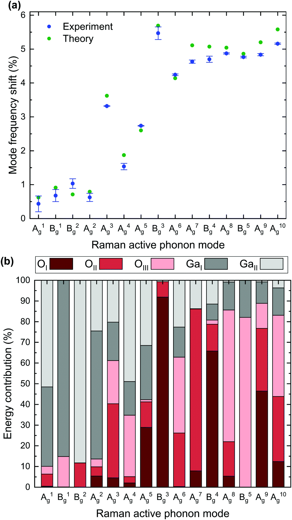 | ||
| Fig. 3 (a) Relative mode frequency shifts of Raman modes for 18O isotope substitution compared to natural isotope distribution based on experimental and theoretical data listed in Table 2. (b) Theoretical calculations of relative energy contributions to the total phonon energy corresponding to each O or Ga lattice site. Raman vibrations can be excited by one of the two Ga (grey) or one of the three O (red) lattice sites. The height of a column indicates the relative energy contribution of the corresponding lattice site. | ||
The analysis of the experimental Raman mode frequency shifts in Fig. 3a reveals several noteworthy results: (i) the relative shift strongly varies between the different modes with the smallest and largest shift of 0.43% for the A1 and 5.47% for the B3, respectively; (ii) low energy phonons between 110 and 170 cm−1 exhibit weak frequency shifts below 1.03%, whereas high frequency phonons with Raman shifts above 350 cm−1 experience large relative shifts close to 5% upon O isotope substitution; (iii) phonons with wavenumbers between 200 and 350 cm−1 show intermediate relative shifts, which do not scale linearly with increasing phonon energy.
Fig. 4 illustrates a scheme of the Raman-active A1, A5 and A10 modes as representatives of the low-energy phonons, phonons of intermediate energies and high-energy-phonons. Modes of A symmetry oscillate within the (010)-plane, with arrows indicating the amplitude of vibration. A scheme of all Raman-active phonon modes is presented in Fig. S3 in the ESI.†
 | ||
| Fig. 4 Scheme of the Raman-active A1, A5 and A10 modes within the primitive unit cell of β-Ga2O3. Modes are shown in projection on the (010)/b-plane. Arrows indicate the displacements of basis atoms, with lengths denoting the amplitude of vibration. Different red and grey colours indicate individual O and Ga lattice site atoms. | ||
In order to explain the reasons for the observations (i)–(iii), we calculate the relative energy contribution of the three oxygen (OI, OII, OIII) and two gallium (GaI, GaII) lattice sites to the total phonon energy for each mode (Fig. 3b). By treating the individual atoms as harmonic oscillators, the displacement of atom k in the x-direction is given by
| xk(t) = Ak·ei·ω·t, | (3) |
The size of the relative frequency shift is dependent upon the contribution of O atoms to the mode intensity. While a large relative frequency shift implies the dominance of O lattice site oscillations within a vibrational mode, a small shift corresponds to the absence of the same. The occurrence of a frequency shift in each of the 15 Raman modes suggests that O vibrations contribute to each phonon mode, which is confirmed by the fact that O lattice sites are present in each mode's energy contribution. Hence, pure Ga–Ga vibrations do not occur.
The smallest relative frequency shifts seen in the low-frequency A1, B1, B2 and A2 modes correspond to a comparatively low energy contribution from O lattice sites to the respective modes. An increased frequency shift relative to the low-frequency modes is distinctive of the A3, A4, A5 and A6 modes. O lattice sites are expected to contribute 61% to the energy of the A3, which is reflected in an observed relative frequency shift of 3.32%. Conversely, a lower frequency shift of 1.54% or 2.74% for the A4 or A5 stems from a less prominent energy contribution from O lattice sites. Oxygen lattice site vibrations are predominant in the B3 and the remaining high-frequency modes from A7 onward and vary between 81% or 99% for the B4 or B3, respectively. Correspondingly, these modes exhibit the greatest mode frequency shifts, with the largest shift observed for the B3.
Finally, we address the impact of oxygen isotope substitutions on the three distinct oxygen lattice sites. A direct comparison of the observed mode frequency shifts and phonon energy contribution of individual lattice sites indicates that the size of the relative frequency shift depends on which of the three O lattice sites contributes to the vibrational mode. The experimental data indicate that replacing 16O with 18O isotopes on the OIII lattice site induces an increased frequency shift compared to OI and OII:
As for the A3 and A6, oxygen vibrations account for 61% or 63% of the mode energy. However, the A6, characterized by a more intense contribution from OIII lattice sites and a reduced contribution from OII sites, has an increased relative frequency shift. Equally, oxygen vibrations account for 86% in the A7 and A8 or 89% in the A9. Yet, the observed frequency shift is most profound for the A8, where OIII lattice sites prevail. As for the B5, the O energy contribution is comprised entirely of OIII sites. Despite a lower overall oxygen contribution (82%) compared to the A7 and B4 modes, the B5 is characterized by an increased relative frequency shift. While the exact values of the computed relative energy contributions may vary slightly depending on the employed XC functional, the above LDA-based conclusions also hold true for PBE, PBEsol and opt-B88.
4 Conclusions
In summary, we examined a homoepitaxial β-Ga2O3 thin film in the 18O isotope composition, deposited on top of a substrate with 16O isotope distribution. Polarized micro-Raman spectroscopy was carried out to record Raman spectra of both isotopologues. By probing the (010) and (01) planes, we were able to separate all 15 Raman active phonon modes and determine their phonon frequencies for both isotopologues. The replacement of 16O with the heavier 18O atoms resulted in a reduction of the phonon frequency. We provided the spectral positions of 18O Raman modes and quantified the absolute as well as relative frequency shifts compared to 16O Raman modes. Based on the comparison of experimental data with DFPT calculations of mode frequency shifts and calculation of the relative energy contributions of each lattice site to the total phonon energy, we identified and quantified the atomistic vibrations for each of the five distinct lattice sites which give rise to the 15 different Raman-active phonon modes in β-Ga2O3. A large relative frequency shift seen in the modes of higher frequencies is emblematic of modes governed predominantly by O lattice site vibrations. In contrast, the low-frequency A1, B1, B2 and A2 modes exhibit the smallest overall shifts and hence are governed by the vibration of both Ga and O atoms. By determining dedicated Raman modes dominated by one of the three inequivalent O-sites and relating their relative frequency shifts to the calculated relative amount each lattice site contributes to a respective mode's energy, we conclude that substituting 16O with 18O isotopes on the OIII lattice site results in an elevated mode frequency shift compared to OI and OII lattice sites. This discovery paves the way for the identification of O-site-related defects by Raman spectroscopy in future studies. Furthermore, micro-Raman spectroscopy may be carried out to investigate the formation of oxygen vacancies in different lattice sites as a function of different synthesis (e.g. deposition, annealing) conditions.
Conflicts of interest
There are no conflicts to declare.Acknowledgements
We acknowledge funding by the Deutsche Forschungsgemeinschaft (DFG, German Research Foundation) – project number 446185170. This work was performed in parts in the framework of GraFOx, a Leibniz-ScienceCampus partially funded by the Leibniz association. Computational resources used for the calculations were provided by the HPC of the Regional Computer Centre Erlangen (RRZE). The authors thank Maximilian Ries for fruitful discussions, Thomas Kure for experimental support, and Arne Haeger for support in graphic design.Notes and references
- N. Ueda, H. Hosono, R. Waseda and H. Kawazoe, Appl. Phys. Lett., 1997, 71, 933–935 CrossRef CAS.
- M. Yamaga, T. Ishikawa, M. Yoshida, T. Hasegawa, E. G. Villora and K. Shimamura, Phys. status, 2011, 8, 2621–2624 CAS.
- S. J. Pearton, J. Yang, P. H. Cary, F. Ren, J. Kim, M. J. Tadjer and M. A. Mastro, Appl. Phys. Rev., 2018, 5, 011301 Search PubMed.
- S. J. Pearton, F. Ren, M. Tadjer and J. Kim, J. Appl. Phys., 2018, 124, 220901 CrossRef.
- M. Higashiwaki, K. Sasaki, A. Kuramata, T. Masui and S. Yamakoshi, Phys. Status Solidi A, 2014, 211, 21–26 CrossRef CAS.
- M. Higashiwaki, K. Sasaki, A. Kuramata, T. Masui and S. Yamakoshi, Appl. Phys. Lett., 2012, 100, 013504 CrossRef.
- M. Higashiwaki, A. Kuramata, H. Murakami and Y. Kumagai, J. Phys. D: Appl. Phys., 2017, 50, 333002 CrossRef.
- Y. Kokubun, K. Miura, F. Endo and S. Nakagomi, Appl. Phys. Lett., 2007, 90, 031912 CrossRef.
- T. Oshima, T. Okuno, N. Arai, N. Suzuki, S. Ohira and S. Fujita, Appl. Phys. Express, 2008, 1, 011202 CrossRef.
- I. Cora, F. Mezzadri, F. Boschi, M. Bosi, M. Čaplovičová, G. Calestani, I. Dódony, B. Pécz and R. Fornari, CrystEngComm, 2017, 19, 1509–1516 RSC.
- R. Roy, V. G. Hill and E. F. Osborn, J. Am. Chem. Soc., 1952, 74, 719–722 CrossRef CAS.
- S. Yoshioka, H. Hayashi, A. Kuwabara, F. Oba, K. Matsunaga and I. Tanaka, J. Phys.: Condens. Matter, 2007, 19, 346211 CrossRef.
- H. von Wenckstern, Adv. Electron. Mater., 2017, 3, 1600350 CrossRef.
- S. I. Stepanov, V. I. Nikolaev, V. E. Bougrov and A. E. Romanov, Rev. Adv. Mater. Sci., 2016, 44, 63–86 CAS.
- H. He, R. Orlando, M. A. Blanco, R. Pandey, E. Amzallag, I. Baraille and M. Rérat, Phys. Rev. B: Condens. Matter Mater. Phys., 2006, 74, 195123 CrossRef.
- H. He, M. A. Blanco and R. Pandey, Appl. Phys. Lett., 2006, 88, 261904 CrossRef.
- P. Kroll, R. Dronskowski and M. Martin, J. Mater. Chem., 2005, 15, 3296 RSC.
- H. Y. Playford, A. C. Hannon, E. R. Barney and R. I. Walton, Chem. – Eur. J., 2013, 19, 2803–2813 CrossRef CAS.
- J. Furthmüller and F. Bechstedt, Phys. Rev. B: Condens. Matter Mater. Phys., 2016, 93, 115204 CrossRef.
- Z. Galazka, R. Uecker, K. Irmscher, M. Albrecht, D. Klimm, M. Pietsch, M. Brützam, R. Bertram, S. Ganschow and R. Fornari, Cryst. Res. Technol., 2010, 45, 1229–1236 CrossRef CAS.
- Z. Galazka, K. Irmscher, R. Uecker, R. Bertram, M. Pietsch, A. Kwasniewski, M. Naumann, T. Schulz, R. Schewski, D. Klimm and M. Bickermann, J. Cryst. Growth, 2014, 404, 184–191 CrossRef CAS.
- K. Irmscher, Z. Galazka, M. Pietsch, R. Uecker and R. Fornari, J. Appl. Phys., 2011, 110, 063720 CrossRef.
- V. I. Vasyltsiv, Y. I. Rym and Y. M. Zakharko, Phys. Status Solidi, 1996, 195, 653–658 CrossRef CAS.
- E. Villora, Y. Morioka, T. Atou, T. Sugawara, M. Kikuchi and T. Fukuda, Phys. Status Solidi, 2002, 193, 187–195 CrossRef CAS.
- N. Suzuki, S. Ohira, M. Tanaka, T. Sugawara, K. Nakajima and T. Shishido, Phys. Status Solidi C, 2007, 4, 2310–2313 CrossRef CAS.
- S. Ohira, N. Suzuki, N. Arai, M. Tanaka, T. Sugawara, K. Nakajima and T. Shishido, Thin Solid Films, 2008, 516, 5763–5767 CrossRef CAS.
- J. Zhang, B. Li, C. Xia, G. Pei, Q. Deng, Z. Yang, W. Xu, H. Shi, F. Wu, Y. Wu and J. Xu, J. Phys. Chem. Solids, 2006, 67, 2448–2451 CrossRef CAS.
- A. Kuramata, K. Koshi, S. Watanabe, Y. Yamaoka, T. Masui and S. Yamakoshi, Jpn. J. Appl. Phys., 2016, 55, 1202A2 CrossRef.
- V. Nikolaev, V. Maslov, S. Stepanov, A. Pechnikov, V. Krymov, I. Nikitina, L. Guzilova, V. Bougrov and A. Romanov, J. Cryst. Growth, 2017, 457, 132–136 CrossRef CAS.
- M. Mohamed, K. Irmscher, C. Janowitz, Z. Galazka, R. Manzke and R. Fornari, Appl. Phys. Lett., 2012, 101, 132106 CrossRef.
- K. Suzuki, T. Okamoto and M. Takata, Ceram. Int., 2004, 30, 1679–1683 CrossRef CAS.
- S. Geller, J. Chem. Phys., 1960, 33, 676–684 CrossRef CAS.
- P. Mazzolini, A. Falkenstein, C. Wouters, R. Schewski, T. Markurt, Z. Galazka, M. Martin, M. Albrecht and O. Bierwagen, APL Mater., 2020, 8, 011107 CrossRef CAS.
- K. Sasaki, A. Kuramata, T. Masui, E. G. Víllora, K. Shimamura and S. Yamakoshi, Appl. Phys. Express, 2012, 5, 035502 CrossRef.
- M. Higashiwaki, K. Konishi, K. Sasaki, K. Goto, K. Nomura, Q. T. Thieu, R. Togashi, H. Murakami, Y. Kumagai, B. Monemar, A. Koukitu, A. Kuramata and S. Yamakoshi, Appl. Phys. Lett., 2016, 108, 133503 CrossRef.
- S. Rafique, M. R. Karim, J. M. Johnson, J. Hwang and H. Zhao, Appl. Phys. Lett., 2018, 112, 052104 CrossRef.
- M.-Y. Tsai, O. Bierwagen, M. E. White and J. S. Speck, J. Vac. Sci. Technol., A, 2010, 28, 354–359 CrossRef CAS.
- G. Wagner, M. Baldini, D. Gogova, M. Schmidbauer, R. Schewski, M. Albrecht, Z. Galazka, D. Klimm and R. Fornari, Phys. Status Solidi A, 2014, 211, 27–33 CrossRef CAS.
- H. Murakami, K. Nomura, K. Goto, K. Sasaki, K. Kawara, Q. Tu Thieu, R. Togashi, Y. Kumagai, M. Higashiwaki, A. Kuramata, S. Yamakoshi, B. Monemar and A. Koukitu, Appl. Phys. Express, 2015, 8, 015503 CrossRef.
- S.-D. Lee, K. Kaneko and S. Fujita, Jpn. J. Appl. Phys., 2016, 55, 1202B8 CrossRef.
- R. Schewski, K. Lion, A. Fiedler, C. Wouters, A. Popp, S. V. Levchenko, T. Schulz, M. Schmidbauer, S. Bin Anooz, R. Grüneberg, Z. Galazka, G. Wagner, K. Irmscher, M. Scheffler, C. Draxl and M. Albrecht, APL Mater., 2019, 7, 022515 CrossRef.
- E. G. Víllora, K. Shimamura, Y. Yoshikawa, T. Ujiie and K. Aoki, Appl. Phys. Lett., 2008, 92, 202120 CrossRef.
- M. Orita, H. Ohta, M. Hirano and H. Hosono, Appl. Phys. Lett., 2000, 77, 4166–4168 CrossRef CAS.
- E. Ahmadi, O. S. Koksaldi, S. W. Kaun, Y. Oshima, D. B. Short, U. K. Mishra and J. S. Speck, Appl. Phys. Express, 2017, 10, 041102 CrossRef.
- W. Zhou, C. Xia, Q. Sai and H. Zhang, Appl. Phys. Lett., 2017, 111, 242103 CrossRef.
- S. C. Siah, R. E. Brandt, K. Lim, L. T. Schelhas, R. Jaramillo, M. D. Heinemann, D. Chua, J. Wright, J. D. Perkins, C. U. Segre, R. G. Gordon, M. F. Toney and T. Buonassisi, Appl. Phys. Lett., 2015, 107, 252103 CrossRef.
- T. Onuma, S. Fujioka, T. Yamaguchi, M. Higashiwaki, K. Sasaki, T. Masui and T. Honda, Appl. Phys. Lett., 2013, 103, 041910 CrossRef.
- M. Baldini, M. Albrecht, A. Fiedler, K. Irmscher, R. Schewski and G. Wagner, ECS J. Solid State Sci. Technol., 2017, 6, Q3040–Q3044 CrossRef CAS.
- J. B. Varley, J. R. Weber, A. Janotti and C. G. Van de Walle, Appl. Phys. Lett., 2010, 97, 142106 CrossRef.
- S. Lany, APL Mater., 2018, 6, 046103 CrossRef.
- J. L. Lyons, Semicond. Sci. Technol., 2018, 33, 05LT02 CrossRef.
- J. Lee, S. Ganguli, A. K. Roy and S. C. Badescu, J. Chem. Phys., 2019, 150, 174706 CrossRef.
- T. Zacherle, P. C. Schmidt and M. Martin, Phys. Rev. B: Condens. Matter Mater. Phys., 2013, 87, 235206 CrossRef.
- A. Kyrtsos, M. Matsubara and E. Bellotti, Phys. Rev. B, 2017, 95, 245202 CrossRef.
- P. Deák, Q. Duy Ho, F. Seemann, B. Aradi, M. Lorke and T. Frauenheim, Phys. Rev. B, 2017, 95, 075208 CrossRef.
- H. Peelaers, J. L. Lyons, J. B. Varley and C. G. Van de Walle, APL Mater., 2019, 7, 022519 CrossRef.
- K. Momma and F. Izumi, J. Appl. Crystallogr., 2011, 44, 1272–1276 CrossRef CAS.
- M. R. Wagner, T. P. Bartel, R. Kirste, A. Hoffmann, J. Sann, S. Lautenschläger, B. K. Meyer and C. Kisielowski, Phys. Rev. B: Condens. Matter Mater. Phys., 2009, 79, 035307 CrossRef.
- A. Kaschner, U. Haboeck, M. Strassburg, M. Strassburg, G. Kaczmarczyk, A. Hoffmann, C. Thomsen, A. Zeuner, H. R. Alves, D. M. Hofmann and B. K. Meyer, Appl. Phys. Lett., 2002, 80, 1909–1911 CrossRef CAS.
- C. Kranert, C. Sturm, R. Schmidt-Grund and M. Grundmann, Sci. Rep., 2016, 6, 35964 CrossRef CAS.
- J. S. Reparaz, E. Chavez-Angel, M. R. Wagner, B. Graczykowski, J. Gomis-Bresco, F. Alzina and C. M. Sotomayor Torres, Rev. Sci. Instrum., 2014, 85, 034901 CrossRef CAS.
- E. Chávez-Ángel, J. S. Reparaz, J. Gomis-Bresco, M. R. Wagner, J. Cuffe, B. Graczykowski, A. Shchepetov, H. Jiang, M. Prunnila, J. Ahopelto, F. Alzina and C. M. Sotomayor Torres, APL Mater., 2014, 2, 012113 CrossRef.
- D. Dohy, G. Lucazeau and A. Revcolevschi, J. Solid State Chem., 1982, 45, 180–192 CrossRef CAS.
- D. Machon, P. F. McMillan, B. Xu and J. Dong, Phys. Rev. B: Condens. Matter Mater. Phys., 2006, 73, 094125 CrossRef.
- B. Liu, M. Gu and X. Liu, Appl. Phys. Lett., 2007, 91, 172102 CrossRef.
- T. Onuma, S. Fujioka, T. Yamaguchi, Y. Itoh, M. Higashiwaki, K. Sasaki, T. Masui and T. Honda, J. Cryst. Growth, 2014, 401, 330–333 CrossRef CAS.
- M. Schubert, R. Korlacki, S. Knight, T. Hofmann, S. Schöche, V. Darakchieva, E. Janzén, B. Monemar, D. Gogova, Q.-T. Thieu, R. Togashi, H. Murakami, Y. Kumagai, K. Goto, A. Kuramata, S. Yamakoshi and M. Higashiwaki, Phys. Rev. B, 2016, 93, 125209 CrossRef.
- C. Kranert, C. Sturm, R. Schmidt-Grund and M. Grundmann, Phys. Rev. Lett., 2016, 116, 127401 CrossRef.
- K. A. Mengle and E. Kioupakis, AIP Adv., 2019, 9, 015313 CrossRef.
- L. Kavan, M. Zukalova, M. Ferus, J. Kürti, J. Koltai and S. Civiš, Phys. Chem. Chem. Phys., 2011, 13, 11583 RSC.
- O. Frank, M. Zukalova, B. Laskova, J. Kürti, J. Koltai and L. Kavan, Phys. Chem. Chem. Phys., 2012, 14, 14567 RSC.
- H. Kaftelen, K. Ocakoglu, R. Thomann, S. Tu, S. Weber and E. Erdem, Phys. Rev. B: Condens. Matter Mater. Phys., 2012, 86, 014113 CrossRef.
- E. Erdem, J. Alloys Compd., 2014, 605, 34–44 CrossRef CAS.
- Ü. Özgür, Y. I. Alivov, C. Liu, A. Teke, M. A. Reshchikov, S. Doğan, V. Avrutin, S. J. Cho and H. Morkoç, J. Appl. Phys., 2005, 98, 041301 CrossRef.
- M. D. McCluskey and S. J. Jokela, J. Appl. Phys., 2009, 106, 71101 CrossRef.
- Y. M. Strzhemechny, H. L. Mosbacker, S. H. Goss, D. C. Look, D. C. Reynolds, C. W. Litton, N. Y. Garces, N. C. Giles, L. E. Halliburton, S. Niki and L. J. Brillson, J. Electron. Mater., 2005, 34, 399–403 CrossRef CAS.
- C. G. Van De Walle, Phys. B, 2001, 308-310, 899–903 CrossRef CAS.
- E. A. Davis, S. P. Cottrell, P. J. King, J. S. Lord, J. M. Gil, H. V. Alberto, R. C. Vilão, J. Piroto Duarte, N. Ayres de Campos, A. Weidinger, R. L. Lichti, S. J. Irvine and S. F. Cox, Phys. Rev. Lett., 2001, 86, 2601–2604 CrossRef.
- A. Kohan, G. Ceder, D. Morgan and C. G. Van de Walle, Phys. Rev. B: Condens. Matter Mater. Phys., 2000, 61, 15019–15027 CrossRef CAS.
- B. K. Meyer, J. Sann, S. Lautenschläger, M. R. Wagner and A. Hoffmann, Phys. Rev. B: Condens. Matter Mater. Phys., 2007, 76, 184120 CrossRef.
- A. Kaschner, U. Haboeck, M. Strassburg, M. Strassburg, G. Kaczmarczyk, A. Hoffmann, C. Thomsen, A. Zeuner, H. R. Alves, D. M. Hofmann and B. K. Meyer, Appl. Phys. Lett., 2002, 80, 1909–1911 CrossRef CAS.
- F. Friedrich and N. H. Nickel, Appl. Phys. Lett., 2007, 91, 111903 CrossRef.
- F. Friedrich, M. A. Gluba and N. H. Nickel, Appl. Phys. Lett., 2009, 95, 141903 CrossRef.
- M. A. Gluba, N. H. Nickel and N. Karpensky, Phys. Rev. B: Condens. Matter Mater. Phys., 2013, 88, 245201 CrossRef.
- L. Artús, R. Cuscó, E. Alarcón-Lladó, G. González-Díaz, I. Mártil, J. Jiménez, B. Wang and M. Callahan, Appl. Phys. Lett., 2007, 90, 181911 CrossRef.
- J. B. Wang, H. M. Zhong, Z. F. Li and W. Lu, Appl. Phys. Lett., 2006, 88, 101913 CrossRef.
- C. Bundesmann, N. Ashkenov, M. Schubert, D. Spemann, T. Butz, E. M. Kaidashev, M. Lorenz and M. Grundmann, Appl. Phys. Lett., 2003, 83, 1974–1976 CrossRef CAS.
- P. Mazzolini, V. Russo, C. S. Casari, T. Hitosugi, S. Nakao, T. Hasegawa and A. Li Bassi, J. Phys. Chem. C, 2016, 120, 18878–18886 CrossRef CAS.
- P. Vogt, O. Brandt, H. Riechert, J. Lähnemann and O. Bierwagen, Phys. Rev. Lett., 2017, 119, 196001 CrossRef.
- O. Bierwagen, P. Vogt and P. Mazzolini, in Gallium Oxide-Materials Properties, Crystal Growth, and Devices, ed. M. Higashiwaki and S. Fujita, Springer International Publishing, Cham, 2020, vol. 293, ch. 6, pp. 95–121 Search PubMed.
- P. Mazzolini, P. Vogt, R. Schewski, C. Wouters, M. Albrecht and O. Bierwagen, APL Mater., 2019, 7, 022511 CrossRef.
- P. Giannozzi, S. Baroni, N. Bonini, M. Calandra, R. Car, C. Cavazzoni, D. Ceresoli, G. L. Chiarotti, M. Cococcioni, I. Dabo, A. D. Corso, S. de Gironcoli, S. Fabris, G. Fratesi, R. Gebauer, U. Gerstmann, C. Gougoussis, A. Kokalj, M. Lazzeri, L. Martin-Samos, N. Marzari, F. Mauri, R. Mazzarello, S. Paolini, A. Pasquarello, L. Paulatto, C. Sbraccia, S. Scandolo, G. Sclauzero, A. P. Seitsonen, A. Smogunov, P. Umari and R. M. Wentzcovitch, J. Phys.: Condens. Matter, 2009, 21, 395502 CrossRef.
- D. R. Hamann, Phys. Rev. B, 2013, 88, 085117 CrossRef.
- M. J. van Setten, M. Giantomassi, E. Bousquet, M. J. Verstraete, D. R. Hamann, X. Gonze and G.-M. Rignanese, Comput. Phys. Comm., 2018, 226, 39–54 CrossRef CAS.
- L. He, F. Liu, G. Hautier, M. J. T. Oliveira, M. A. L. Marques, F. D. Vila, J. J. Rehr, G.-M. Rignanese and A. Zhou, Phys. Rev. B: Condens. Matter Mater. Phys., 2014, 89, 064305 CrossRef.
- J. Åhman, G. Svensson and J. Albertsson, Acta Crystallogr., Sect. C: Cryst. Struct. Commun., 1996, 52, 1336–1338 CrossRef.
- K. Yamaguchi, Solid State Commun., 2004, 131, 739–744 CrossRef CAS.
- P. Mazzolini and O. Bierwagen, J. Phys. D: Appl. Phys., 2020, 53, 354003 CrossRef CAS.
- M. Cardona and M. L. W. Thewalt, Rev. Mod. Phys., 2005, 77, 1173–1224 CrossRef CAS.
- M. D. McCluskey, J. Appl. Phys., 2000, 87, 3593–3617 CrossRef CAS.
Footnote |
| † Electronic supplementary information (ESI) available. See DOI: 10.1039/d0tc04101g |
| This journal is © The Royal Society of Chemistry 2021 |