
 Open Access Article
 This Open Access Article is licensed under a Creative Commons Attribution-Non Commercial 3.0 Unported Licence
Crystallization driven boost in fill factor and stability in additive-free organic solar cells†
David
Garcia Romero
 ,
Lorenzo
Di Mario
,
Giuseppe
Portale
and
Maria Antonietta
Loi
*
,
Lorenzo
Di Mario
,
Giuseppe
Portale
and
Maria Antonietta
Loi
*
Zernike Institute for Advanced Materials, University of Groningen, Nijenborgh 4, Groningen 9747 AG, The Netherlands. E-mail: m.a.loi@rug.nl
First published on 11th October 2021
Abstract
The control of morphology and microstructure during and after the active layer processing of bulk-heterojunction solar cells is critical to obtain elevated fill factors and overall good device performance. With the recent development of non-fullerene acceptors, wide attention has been paid to improve miscibility, solubility and nanoscale separation by laborious molecular design processes and by the use of additives. Nonetheless, several post-processing strategies can equally contribute to obtain an optimum phase separation and even to an enhanced crystallinity, but their effect on performance and device lifetime of polymer/non-fullerene acceptor solar cells is still unclear. Herein, we report a systematic comparison between different post-processing treatments including thermal annealing (TA), vacuum drying (VD) and solvent vapor annealing (SVA) on the TPD-3F polymer and IT-4F non-fullerene acceptor, comparing their effects on device performance as well as on the morphology and optical and electrical properties. The optimized SVA treated devices exhibited power conversion efficiencies close to 14% with a remarkable 76% fill factor and superior short-circuit currents compared to the one of untreated devices. Moreover, SVA demonstrated improvements in device stability both under illumination and under ambient conditions. The induced phase separation and the increased crystallinity of the acceptor molecules, as revealed by GIWAXS measurements, led to increased photogenerated currents, with a more effective exciton dissociation and charge collection. The open-circuit voltage losses in the SVA and TA devices were explained by a bandgap reduction and a higher trap-assisted recombination, respectively. Overall, our study points to the role of post-processing in organic solar cell fabrication, and contributes towards a new generation of efficient and stable additive-free organic solar cells.
Introduction
Solution-processed organic solar cells (OSCs) have recently gained enormous interest, thanks to the development of non-fullerene acceptors (NFAs), leading to record efficiencies over 18%.1 In general, the chemical tuneability, the easy thin film deposition, and the high absorption in the visible spectral region make these materials very promising for solar cell fabrication. On the other hand, the mostly amorphous nature of these small molecule thin films usually gives rise to poor blend morphologies, leading to low mobilities and high recombination rates.2 Hence, the nanoscale phase separation and the crystallinity mostly determine the exciton dissociation and charge transport, and ultimately the photovoltaic performance.2,3 Moreover, the domain size, domain purity and molecular stacking have an important impact on the most elusive solar cell parameter, the fill factor (FF), which is usually very challenging to predict and boost in OSCs.4 While over 80% FFs have been reported for other emerging photovoltaic technologies such as perovskite-based solar cells, even the state-of-the art reported organic solar cells struggle to achieve FFs over 75%.5,6A common strategy to control donor and acceptor phase segregation in order to boost the FF and overall performance is the use of additives. However, there is a strong concern about their adoption for industrial production, similar to the use of halogenated solvents, as most of them are toxic or harmful to the environment. Moreover, additive residuals have been shown to have negative effects on the device lifetime due to faster morphological deterioration.7,8 Conversely, post-processing treatments can provide significant improvements in performance even in the absence of additives. The extensively used thermal annealing (TA) often improves the morphology of the components inducing a controlled de-mixing.9 The vacuum drying (VD) method has been recently shown to improve solvent removal, giving rise to smoother films and enhanced photovoltaic performance.10 Finally, solvent vapor annealing (SVA) has been demonstrated to enable further control of both phase separation and crystallinity.3,11
In the first generation of OSCs, where fullerene derivatives were employed, these methods were extensively used and many systematic studies are present in the literature.12–14 Also, in the second generation of OSCs, namely the one based on all-small-molecules, the crucial role of post-processing for morphological optimization has been widely reported.9,15,16 Conversely, research on the third generation of OSCs, where non-fullerene acceptors (NFAs) are used, has somehow disregarded the importance of the control of crystallization and the microstructure.
Recently, Datt et al. showed the superior effectiveness of SVA over TA for several polymer/NFA combinations. Nonetheless, in their study the device lifetime was not considered and additives were employed to obtain efficiencies over 9%.17 More recently, the influence of these treatments on the microstructure of record-efficient D18/NFA blends demonstrated the relevance of post-processing in high-performance OSCs. However, also in this case the device lifetime was not investigated, missing an important verification check towards possible implementation in real life products.18 Actually, while the importance of operational stability and the need for lifetime measurement consensus are on the rise,19 its correlation with the active layer morphology for NFA OSCs is still not seldomly investigated.20 Overall, despite the wide adoption of these strategies, a complete picture that correlates the morphological changes with all the device parameters using a reproduceable process and a proper investigation of their influence on device stability are still missing for polymer/NFA OSCs.
Therefore, our study focuses on the effect on photovoltaic, optical, morphological and electrical properties of three different post-processing methods employed for additive-free bulk-heterojunction (BHJ) OSCs. The commercially available poly[[2,2′-[[4,8-bis[4-fluoro-5-(2-hexyldecyl)-2-thienyl]benzo[1,2-b:4,5-b′]dithiophene-2,6-diyl]-2,5-thiophenediyl(5,6-dihydro-5-octyl-4,6-dioxo-4H-thieno[3,4-c]pyrrole-1,3-diyl)-2,5-thiophenediyl] (TPD-3F) was used as a donor candidate due to its recently reported suitability to fabricate high performance BHJ OSCs with potential for device scalability.21,22 As for a non-fullerene acceptor, we used the well-known small molecule 3,9-bis(2-methylene-((3-(1,1-dicyanomethylene)-6,7-difluoro)-indanone))-5,5,11,11-tetrakis(4-hexylphenyl)-dithieno[2,3-d:2′,3′-d′]-s-indaceno[1,2-b:5,6-b′]dithiophene (IT-4F) due to its deep molecular levels and easy processability. It is one of the most widely used NFAs, nowadays. Moreover, these materials have shown efficiencies up to ∼14% in binary BHJ solar cells using 1,8-diodoctane as an additive and with an inverted structure,21 and up to 17% when used in ternary solar cells,22 showing remarkable stabilities as well. It is important to underline that not only stability, simple materials synthesis, the fabrication from environmentally friendly solvents and efficiency should be considered when evaluating the relevance of an active layer for future industrialization.
In this work, differences in the performance of solar cells when the TPD-3F/IT-4F active layer was treated with VD, TA and SVA compared to the as-cast (AC) condition are directly correlated with modifications of the blend nanostructure. Devices with SVA showed the highest performance, as a result of an increase in JSC and FF, which made up for a slightly reduced VOC as compared with that of the control sample. Grazing incidence wide-angle X-ray scattering (GIWAXS) showed that the induced aggregation due to prominent acceptor crystallization upon SVA is at the origin of the increased exciton dissociation and charge collection, leading to a high JSC and FF. Nonetheless, the increased molecular packing promotes the reduction of the energy band-gap, leading to a decrease of ∼30 mV in VOC. The correlation between the morphology and performance is further confirmed by impedance spectroscopy and photoluminescence measurements. Overall, an increase of PCE from 11.31% for AC devices to 13.84% is achieved by using an optimized SVA procedure. This result is on par with the best results reported in the literature for the same donor and acceptor when additives are used.21 Remarkably, with a FF = 76% and a VOC = 0.911 V, our champion device showed, to the best of our knowledge, the highest reported combination of these parameters for efficient and additive-free BHJ solar cells. In addition, the influence of post-deposition strategies on the device stability was evaluated under continuous illumination and under long term storage, both under inert and under ambient conditions, as recommended by the stability ISOS test guidelines.19,23 In contrast to the as-cast devices, those treated with SVA were found to maintain ∼75% of their initial PCE after >35 h of light soaking at 1 sun illumination, and showed improved lifetimes under ambient conditions.
Results and discussion
As shown in the schematic of Fig. 1a, after spin-coating an active layer composed of TPD-3F and IT-4F from a chloroform solution, three different post-processing treatments were applied: (i) vacuum-assisted drying (VD) for 2 h, (ii) thermal annealing (TA) at 120 °C and (iii) solvent vapor annealing (SVA) with chloroform. The chemical structures of the TPD-3F donor and of the IT-4F acceptor are shown in Fig. 1b. The ultraviolet-visible (UV-Vis) absorption spectra of both compounds in thin films (Fig. 1c) show complementary absorption in the visible region with an estimated optical band gap (Eoptg) of 1.87 eV for the polymer and 1.55 eV for the small molecule. The normalized absorption spectra of the blends show that SVA induces a red-shift of ∼40 meV in the acceptor peak, while VD and TA have a negligible effect on the peak position (Fig. 1d). In agreement with the absorption, the photoluminescence spectra of the SVA treated sample, also show a red-shift. Furthermore, the effect of the SVA treatment is also observed for the neat acceptor film, while no change is found for the donor polymer (Fig. S1†). Such a change in the optical response suggests that the acceptor small molecules face a strong conformational modification upon the swelling of chloroform vapors, leading to morphological changes in both blend and neat material films. A similar observation was previously reported for fullerene acceptors.9,24 | ||
| Fig. 1 (a) Schematic representation of the post-processing methods used after spin-casting the BHJ active layer. (b) Molecular structures of small molecule acceptor IT-4F and polymer donor TPD-3F. Normalized UV-Vis absorption spectra of the neat material films (c) and of the blend for each post-processing treatment together with the photoluminescence emission (d). The followed color code is defined in panel (a). | ||
To understand the influence of post-processing on the photovoltaic performance, we fabricated solar cells using a conventional stack composed of ITO/PEDOT:PSS/active layer/PDIN/Ag. The organic layer thickness was maintained at ∼130 nm. Fig. 2a shows the J–V curves under AM 1.5 illumination and the measured power conversion efficiencies (PCE). As shown in Table 1, all post-processing treatments have a positive impact on the device performance. The VD method led to a maximum VOC of 0.949 V with enhanced FF and JSC as compared to the AC condition, as well as improved reproducibility, as shown in the inset of Fig. 2a. The other two methods have an even stronger impact on the JSC and FF, exhibiting maximum values of 19.2 mA cm−2 and 69% for the TA devices, and 20.3 mA cm−2 and 76% for the SVA ones. The latter condition led to a champion device PCE of 13.8%, yielding a record combination of VOC and FF in comparison to those of previously reported high-efficiency additive-free BHJ OSCs (Fig. S2†). Moreover, an enhancement of the reproducibility was also observed for SVA devices. Nevertheless, in contrast to AC and VD, the other two methods prompted a reduction in VOC. This detrimental effect of TA and SVA treatments on BHJs has been ascribed by some researchers to the narrowing of the quasi-Fermi level splitting and the increase of crystallinity,15,24 while others attribute it to an increase of energetic disorder leading to higher recombination losses.16
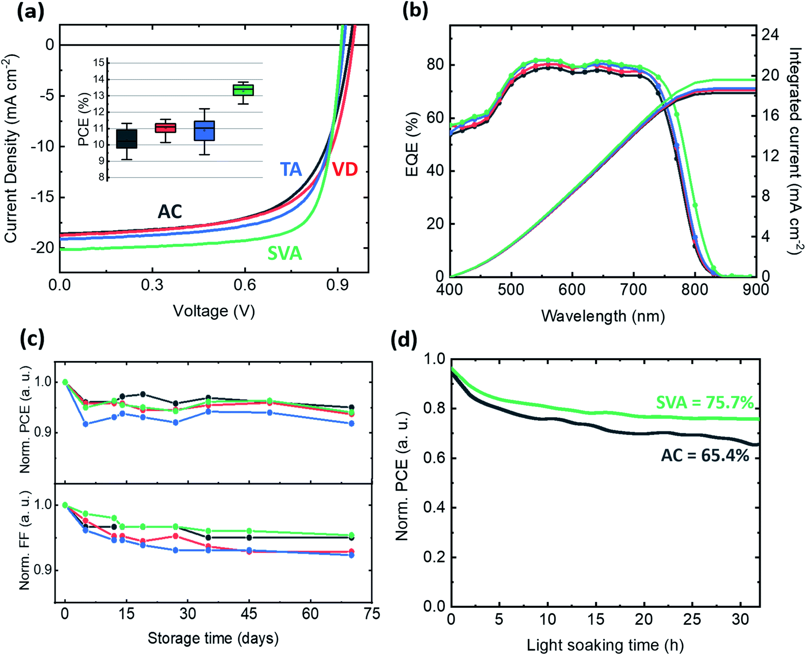 | ||
| Fig. 2 (a) J–V characteristics of the best device with the as-cast (AC), vacuum dried (VD), thermally annealed (TA) and solvent vapor annealed (SVA) active layer; in the inset is shown the distribution of PCE over 15 different devices for each condition. (b) External quantum efficiency (EQE) and integrated short-circuit currents for all four conditions. (c) Normalized PCE and FF over 70 days of storage under nitrogen conditions. (d) Power conversion efficiency at maximum output power tracked over 30 hours under continuous illumination (100 mW cm−2). | ||
| Post-treatment | V OC (V) | J SC (mA cm−2) | FF (%) | PCE (%) |
|---|---|---|---|---|
| As-cast | 0.942 (0.928 ± 0.024) | 18.62 (18.20 ± 0.33) | 65 (60.8 ± 2.6) | 11.31 (10.28 ± 0.69) |
| VD | 0.949 (0.937 ± 0.006) | 18.87 (18.40 ± 0.28) | 66 (63.4 ± 2.5) | 11.56 (10.94 ± 0.39) |
| TA | 0.927 (0.884 ± 0.040) | 19.23 (18.80 ± 0.28) | 69 (64.1 ± 2.9) | 12.21 (10.69 ± 0.81) |
| SVA | 0.911 (0.901 ± 0.004) | 20.25 (20.0 ± 0.14) | 76 (73.8 ± 2.0) | 13.84 (13.29 ± 0.41) |
Fig. 2b shows the external quantum efficiency (EQE) spectra and the calculated JSC for all four post-processing conditions. A similar shape is found for AC, VD and TA devices, whereas the SVA ones show a clear extension in the low energy edge of the spectrum leading to an increased JSC. Hence, a shift in the acceptor energy levels appears to be beneficial for photocurrent generation. The systematic increase of the EQE in the whole visible region suggests an enhanced charge generation and transport in donor and acceptor domains upon post-treatment.
The effect of post-processing on device stability is shown in Fig. 2c, d and S3.† Non-encapsulated samples stored under nitrogen conditions for over 70 days show a well-maintained PCE of ∼95% of the initial value, except for the TA device, which shows efficiencies close to 90% of the initial value. The improvement in the fill factor of VD and TA devices does not translate into a better stability with storage time than the reference AC device. Conversely, SVA is able to maintain both the PCE and the FF at a closer level to those of the fresh device. For this reason, the maximum output power delivered by AC and SVA devices was tracked over time under 1 sun illumination conditions (Fig. 2d). A constant value of ∼75% of the initial PCE after more than 35 h of light soaking was measured for SVA devices, while for AC devices a value of ∼65% was measured at the end of the test.
The interaction between the photoactive layer and the acidic PEDOT:PSS interlayer is known to induce degradation in OSCs, especially under ambient conditions due to its hygroscopicity.19,25 Recently, Hu et al. showed that the high diffusion coefficient of IT-4F leading to high crystal growth rates can bring device stability problems.20 On the contrary, our results show that the optimized SVA treated devices have an improved stability both under light soaking and when aged. Even when stored under air conditions at 45% of relative humidity (RH), SVA devices proved to be more stable than their AC counterparts (Fig. S3†). We speculate that the induced molecular configuration closer to the thermodynamic equilibrium obtained with SVA might be the reason why the typical burn-in degradation region is much less profound than in the AC.26
To understand if the source of the observed differences in absorption, device performance and stability is due to induced structural changes, grazing incidence wide-angle X-ray scattering (GIWAXS) measurements were performed. Fig. S4† shows the GIWAXS patterns and the corresponding plane cuts of the neat TPD-3F and IT-4F films, with and without SVA. The donor was found to have a preferential face-on molecular orientation with respect to the substrate. Both conditions showed a π–π stacking attributed to the (010) reflection with an interplanar distance of 3.3 Å. However, both the (010) and the lamellar (100) peak located at qxy = 0.29 Å−1 corresponding to the donor alkyl-chain periodicity were weakened with SVA. In contrast, the SVA method caused an increase in the scattering intensity in both the in-plane and the out-of-plane directions of the poorly ordered acceptor film. Using the Scherrer analysis, the apparent crystallite size or correlation length was calculated using CCL = 2π/FWHM, where FWHM is the full width of the half maximum of the peak.27 Considering the weak (100) peak at qxy ∼ 0.4 Å−1 as a signature of the acceptor alkyl-chain periodicity, the crystallite size increases from 9.7 Å to 38.2 Å when SVA is applied. This evidences a large impact of SVA on the acceptor molecules with a subsequent increase in the degree of molecular packing. Moreover, the increase of the signal at low qz proves that both face-on and edge-on orientations are promoted with the SVA treatment, suggesting that the bulk of the film moves from a disordered to a more crystalline nature.
Fig. 3 shows the 2-D diffraction patterns of the blends deposited on top of the hole transport layer for the four conditions considered in this work. The prominent in-plane reflection at qxy ∼ 0.3 Å−1 coming from the polymer crystallites demonstrates that the preferential face-on molecular orientation is preserved. The contribution of the acceptor to the blend crystallinity seems minimal for the first three conditions. The correlation length corresponding to the donor periodicity on the blends increased from 33.05 Å to 39.90 Å by VD and to 35.34 Å by TA. However, the reduction of peak intensity observed for TA samples suggests a decrease in the amount of the polymer ordered phase in the blend. As expected, the correlation length of that reflection attributed to the donor reduced to 28.56 Å by SVA. However, this condition showed a new reflection peak at qxy = 0.38 Å−1 which can be attributed to the IT-4F crystallites. It is well-known that efficient charge transport in conjugated systems is strongly correlated with the extent of π–π stacking.28 The observed increase in the (010) peak when SVA is applied can be correlated with the increase of acceptor packing in the face-on orientation, which is located close to the donor (010) reflection at qz ∼ 1.9 Å−1. This means that the SVA treatment promotes the presence of acceptor crystallites, which might improve the electron transport and therefore explain the increase of JSC and FF. As a consequence of the higher intermolecular overlap between π orbitals, as evidenced by the higher presence of π–π stacking, the exciton delocalization in the acceptor increases, determining the red-shift of the absorption edge.29
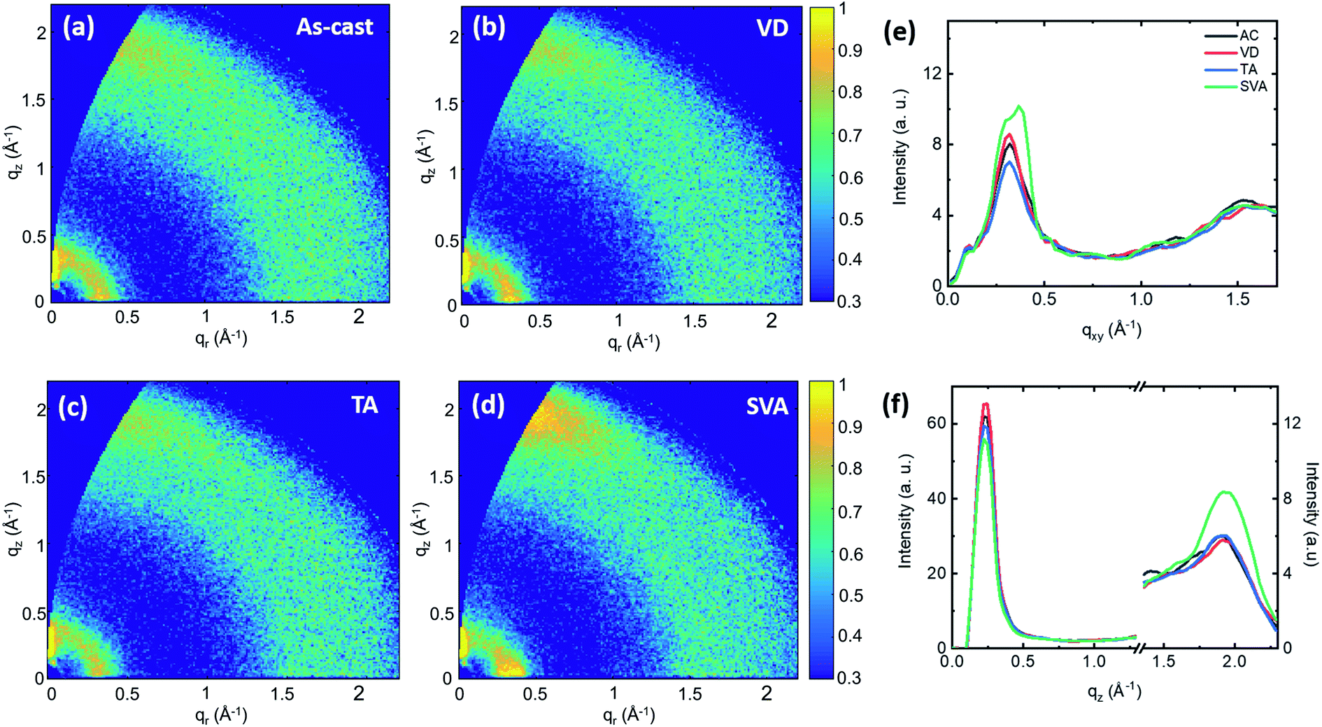 | ||
| Fig. 3 GIWAXS 2-D images (a–d) and their corresponding in-plane (e) and out-of-plane (f) line cuts. | ||
The increased molecular packing is in agreement with the bigger domains observed in surface topographical images, taken via an atomic force microscope (AFM) (Fig. S5†). The calculated root mean square (RMS) roughness is slightly increased by the SVA treatment, however, not in a degree to become detrimental for the interface with the transport layer.
From these results it can be concluded that SVA induces both phase separation and crystallization of acceptor molecules in the blend. This leads to changes in the energy levels, as observed by the absorption red-shift and to a more efficient vertical charge transport, ultimately determining an improved JSC and FF. Finally, the higher molecular packing with more crystalline domains in the vapor annealed devices might reduce the contact with spurious molecules and consequently the number of photo-chemical reactions occurring over time in this sample, which would explain the improved stability observed in Fig. 2.26
In order to understand the implications of these morphological changes for device performance, exciton dissociation, light power dependence and capacitance measurements were performed. Moreover, series and shunt resistances were calculated from the measured J–V under dark conditions and are shown in Table 2. Fig. 4a shows the behavior of the calculated JPH with respect to Veff for all the four conditions of the active layer. JPH corresponds to the difference between light and dark current densities, and V0 is defined as the applied voltage at which the two current densities compensate. For large effective voltage (Veff = V0 − Vapp), where photon harvesting is maximized, the JPH reaches a saturation plateau (JPH,sat). The ratio between JPH and JPH,sat under short-circuit conditions and under maximum output power conditions can be correlated with the dissociation probability (Pdiss) and to the charge collection probability (Pcoll), respectively.30 SVA devices showed a remarkable Pdiss = 98.6% and a Pcoll = 87.9%, suggesting that a large fraction of the photogenerated excitons in both donor-rich and acceptor-rich domains can effectively reach the interface, dissociate into free charges and be collected at the electrodes (Table 2). This is in agreement with the improved morphology and lower series resistance, as observed in the J–V curve measured under dark conditions (Fig. 4b). In fact, the likely higher offset between the LUMO levels at the donor–acceptor interface contributes to a higher driving force for exciton dissociation. However, the slightly worsened roughness could lead to higher leakage currents for SVA devices when compared to VD and TA ones. In contrast, for devices with an AC active layer, a Pcoll,AC of 77.5% together with a high shunt current matches with their low device performance. The optimum solvent removal obtained by the vacuum-assisted drying process led VD devices to have a lower leakage current, resulting in an improved FF and performance in comparison to the AC sample. The lowest Pdiss was exhibited by the TA devices, indicating a higher geminate recombination. A high JSC and FF are still observed for this condition due to the efficient charge collection and low shunt current.
| P diss (%) | P coll (%) | R S (Ω cm−2) | R SH (kΩ cm−2) | |
|---|---|---|---|---|
| As-cast | 97.4 | 77.5 | 1.074 | 2.196 |
| VD | 98.1 | 80.2 | 1.066 | 13.05 |
| TA | 96.8 | 80.8 | 0.762 | 22.62 |
| SVA | 98.6 | 87.9 | 0.568 | 5.638 |
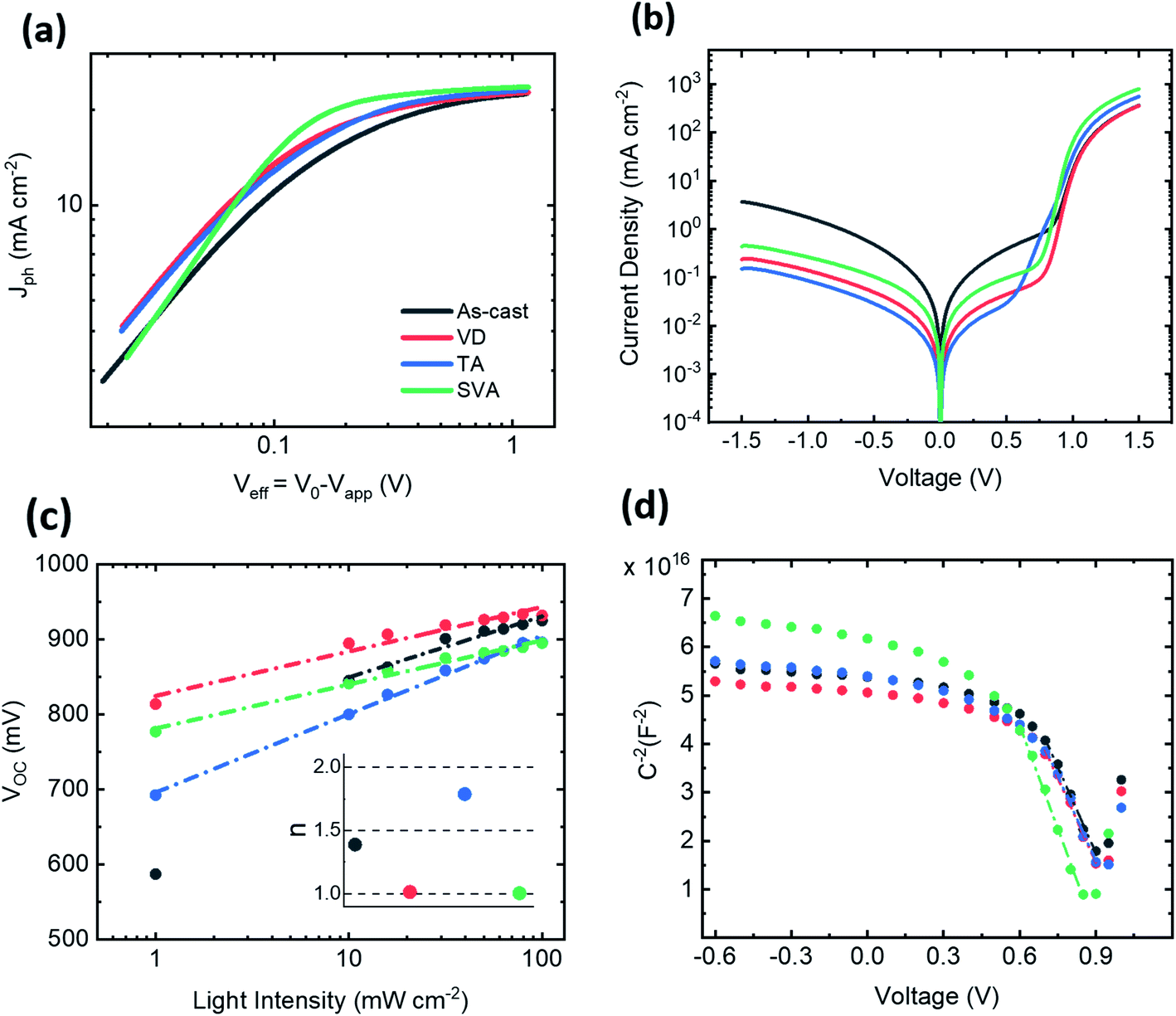 | ||
| Fig. 4 (a) Photocurrent density (JPH) as a function of effective voltage (Veff = V0 − Vapp). (b) Dark J–V curves. (c) Open-circuit voltage as a function of light intensity; the inset shows the diode ideality factor (n). (d) Capacitance as a function of applied voltage. | ||
The recombination mechanisms governing the bulk transport were evaluated by light-dependent measurements (Fig. 4c and S6†). The JSC was found to increase almost linearly with the light intensity for all the conditions (Fig. S6†), suggesting a low bimolecular recombination.31 The diode ideality factor (n) can be extracted from the slope of VOCversus the light intensity, where it is assumed that the system follows a diode behavior. It is usually considered that a slope close to kBT/q means dominance of bimolecular or surface trap-assisted recombination, while a slope values near 2 kBT/q account for dominance of trap-assisted recombination.32 For the SVA and VD conditions, a near-unity factor was extracted, while AC and TA exhibited n = 1.4 and n = 1.7, respectively. At low light intensities, the effect of leakage and the VOC dependence on the dark current can lead to deviations from the linear dependence.33 This can be seen for the AC samples, due to their prominent shunt current. The high n under the TA conditions, together with the larger increase in the forward bias of the dark J–V curves, suggests a large degree of trap-assisted recombination, which is in agreement with the lower dissociation probability and the large VOC losses.
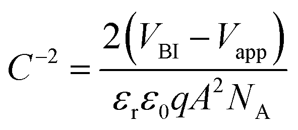
To see how the changes in morphology affect the space-charge region, we evaluated the capacitance of our devices under different bias conditions (Fig. 4d) by using impedance spectroscopy (IS). For reverse applied voltage, the space-charge region is fully depleted and the capacitance is solely governed by the dielectric contribution. At high forward bias, the chemical capacitance dominates due to the excess of injected charges. Finally, for intermediate forward bias, the applied voltage modulates the width of the space-charge region and it can be fitted with the Mott–Schottky relation expressed as
 | (1) |
To correlate the exciton dynamics with the microstructure, we conducted steady-state and time-resolved PL experiments (Fig. 5). An excitation energy of 400 nm was used to excite both components in the BHJ and neat films. The non-normalized absorption and PL emission spectra of the samples are shown in Fig. S7,† where all the samples had a thickness of 130 ± 10 nm. The effective quenching (>95%) of PL observed for all conditions is in agreement with the high dissociation probability values. However, as observed in Fig. S7,† the SVA condition gave the highest absolute emission. Here it is important to understand that special care was taken to carry out the measurements under similar conditions, so that the absolute values of the PL intensity can be compared. When it comes to bulk-heterojunctions, an increase of radiative emission in the PL spectra is typically due to the excitons not being able to reach the D–A interface.37 In the case of samples with SVA, the increase of crystalline domains, as observed by GIWAXS and AFM, leads to a higher rate of excitons recombining radiatively before reaching the interface. Secondly, the higher PL quenching exhibited by the blend treated with TA could be explained by both a decrease in the domain size and an increase in non-radiative recombination through trap-states. While a quantitative evaluation of the recombination is out of the scope of this work, a higher trap density promoted by TA can be correlated with the observed lower dissociation probability and the high VOC losses of the samples treated with TA. No significant differences have been observed in PL emission between AC and VD, confirming that vacuum drying has minimal or no effect on the domain size and purity.
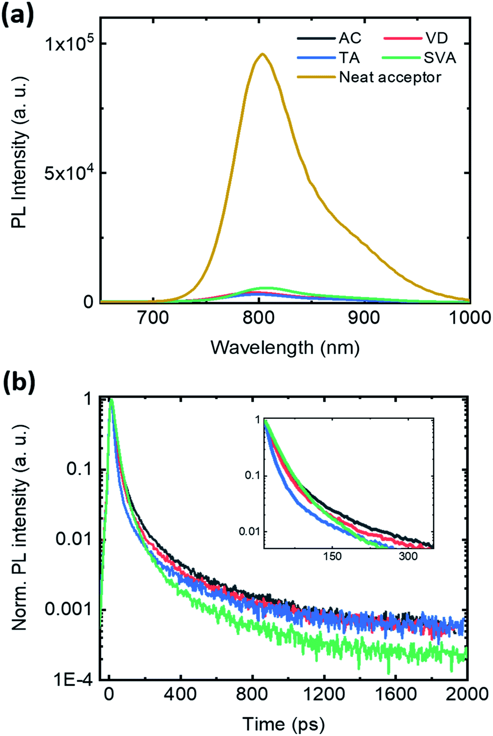 | ||
| Fig. 5 Steady-state (a) and time-resolved (b) photoluminescence (PL) of the IT-4F film and TPD-3F:IT-4F solar cells excited at 400 nm. The time resolved traces are integrated over the whole spectra. | ||
Finally, the time-resolved PL shows that excitons undergo a faster quenching in SVA samples as observed by the rapid decay in comparison to the other conditions (Fig. 5b). The extracted lifetimes are listed in Table S2.† This observation is in agreement with the improved morphology and high JSC and FF. However, a faster decay time is observed for TA within the first 150 ps, while for longer times no significant differences are observed with respect to the AC and VD conditions. This can explain that, even though the smaller domain size promotes a faster exciton population decrease, the morphology promoted by TA generates inefficient exciton dissociation in a larger time scale, yielding lower device performance in comparison to the SVA.
Conclusions
To sum up, this work demonstrates the effectiveness of different post-treatment methods to enhance the performance and the stability of additive-free BHJ solar cells based on TPD-3F and IT-4F. The SVA strategy produced IT-4F aggregation and crystallization in the blend, improving the bulk morphology for exciton dissociation, and leading to a remarkable FF of 76% and a PCE of 13.84%. The observed VOC reduction in SVA devices is explained by a reduction in the energy bandgap due to the increase in the acceptor molecular packing. On the other hand, the VOC losses in TA devices are explained by an increase in trap-assisted recombination, which, anyhow, did not hinder the improvement in device performance in comparison to that of the AC control sample. Additionally, SVA gave rise to stability improvements, maintaining a PCE of ∼95% after 70 days of storage and 75.6% of the initial PCE after >35 h of continuous illumination, in contrast to 65.4% of the control sample. These results manifest the potential of post-processing to prevent the use of additives in NFA-based OSCs and simultaneously boost the performance and stability.Experimental
Materials
TPD-3F and IT-4F were purchased from Raynergy Tek. PEDOT:PSS water dispersion (Clevios VP AI 4083) was acquired from Heraeus and PDIN (98%) from Ossila. MeOH (99.8%), AcOH (≥99%) and CF (≥99%) were purchased from Sigma Aldrich. All the materials were used without further purification.Solar cell fabrication
Solar cells with a conventional structure ITO/PEDOT:PSS/TDP-3F:IT-4F/PDIN/Ag were fabricated on pre-patterned glass substrates. An active layer solution was prepared with a polymer concentration of 6 mg ml−1 (1![[thin space (1/6-em)]](https://www.rsc.org/images/entities/char_2009.gif) :1) in CF and stirred at 40 °C for 12 h. The PDIN solution was prepared with 1 mg ml−1 in MeOH:AcOH (1000:3) and stirred at RT for the same time as that of the active layer solution. After cleaning with soapy water, de-ionized water, acetone and isopropyl alcohol, the substrates were dried and subjected to UV/ozone treatment for 30 min. PEDOT:PSS was spin-coated at 4000 rpm in air and annealed at 140 °C for 20 min, forming ∼40 nm layers. Afterwards, the active layer was spin coated in a N2 atmosphere at 4000 rpm for 30 s, forming a BHJ film with ∼130 nm thickness. Next, some samples were thermally annealed at 120 °C for 10 min. Samples for vacuum drying were transferred to a vacuum chamber for 2 h. Finally, solvent annealed samples were produced by dropping 20 ml of CF inside a Petri dish with the as cast film and left closed for 5 min. The PDIN transport layer was formed equally on all samples by dynamic spin-coating at 1500 rpm without any annealing. Finally, a 100 nm Ag layer was thermally evaporated at ∼10−7 mbar.
:1) in CF and stirred at 40 °C for 12 h. The PDIN solution was prepared with 1 mg ml−1 in MeOH:AcOH (1000:3) and stirred at RT for the same time as that of the active layer solution. After cleaning with soapy water, de-ionized water, acetone and isopropyl alcohol, the substrates were dried and subjected to UV/ozone treatment for 30 min. PEDOT:PSS was spin-coated at 4000 rpm in air and annealed at 140 °C for 20 min, forming ∼40 nm layers. Afterwards, the active layer was spin coated in a N2 atmosphere at 4000 rpm for 30 s, forming a BHJ film with ∼130 nm thickness. Next, some samples were thermally annealed at 120 °C for 10 min. Samples for vacuum drying were transferred to a vacuum chamber for 2 h. Finally, solvent annealed samples were produced by dropping 20 ml of CF inside a Petri dish with the as cast film and left closed for 5 min. The PDIN transport layer was formed equally on all samples by dynamic spin-coating at 1500 rpm without any annealing. Finally, a 100 nm Ag layer was thermally evaporated at ∼10−7 mbar.
Photovoltaic characterization
The J–V characteristics were obtained at a constant temperature of 295 K using a Keithley 2400 source meter, under simulated AM 1.5 G solar illumination from a Steuernagel solar constant 1200 metal halide lamp. A monocrystalline silicon solar cell (WRVS reference cell, Fraunhofer ISE) was used for calibration and corrected for spectral mismatch. The illuminated areas were confined by a shadow mask (0.04 cm2). To measure the external quantum efficiency (EQE), a home built set-up was used. The light from a xenon lamp was guided through a set of three filter wheels which allowed measurements in the spectral range of 400–1400 nm at 20 nm intervals below 680 nm and 30 nm intervals above 680 nm. After the filter wheels, the light was chopped and focused on the sample. The measurement was performed on the samples in a nitrogen atmosphere. The obtained photocurrent was measured using a lock in amplifier (Stanford Research Systems, Model SR830 DSP Lock-In Amplifier). Prior to the measurement of the samples, the photon flux was calibrated using a set of Newport optical power detectors (Newport Model 818-SL and Model 818-IR).Impedance
Impedance measurements were conducted under dark conditions on a Solarton 1260 impedance gain-phase analyzer. The AC drive voltage was maintained at 10 mV. For C–V measurements, a frequency of 10 kHz and a DC voltage in the range of −0.8 to 1.2 V were used.Absorption and photoluminescence
The absorption spectra of each type of the organic film were obtained on a Shimadzu UV-3600 UV-Vis-NIR spectrometer. Steady state and time-resolved luminescence were measured on organic films on top of the HTL (PEDOT:PSS) in reflection geometry and with the samples in a nitrogen atmosphere. The samples were excited using the second harmonic (400 nm) of the emission from a Coherent Mira 900 Ti:sapphire laser, with an average power of 50 μW. A combined spectrometer, constituted by a monochromator with a 1200 mm−1 grating and two detectors, was used to measure the photoluminescence of the samples. A Hamamatsu C9100-13 spectral-calibrated EM-CCD camera was used to acquire the steady state spectra, while for time-resolved measurements a Hamamatsu C5680-24 picosecond streak camera, working in synchro scan mode, was employed. A time resolution of 2 ps was evaluated measuring the scattered laser light.Morphology and thickness
The AFM images were taken with a Bruker microscope (MultiMode 8 with ScanAsyst) in ScanAsyst peak force tapping mode with SCANASYST-AIR probes. GIWAXS measurements were performed using a MINA instrument, an X-ray scattering equipment built on a rotating copper anodic source (wavelength = 1.5413 Å). The measured 2-D patterns were collected using a Vantec500 detector using a 1024 × 1024 pixel array (pixel size = 136 × 136 μm) at a distance of 99.5 mm from the sample. The thin films were placed in reflection geometry at a certain incident angle ai with respect to the direct beam using a Huber goniometer. An incident angle of 0.2 was used. 30 min of exposure time per pattern was used. The direct beam centre position on the detector and the sample-to-detector distance were calibrated using the diffraction rings from standard silver behenate and Al2O3 powders. GIWAXS experimental patterns were converted to the calibrate images using Matlab. A profilometer (Dektak 6M Stylus Profiler Veeco) was used to calibrate the thickness of the active layer and interlayers.Conflicts of interest
The authors declare no conflict of interest.Acknowledgements
The authors kindly thank A. F. Kamp and T. Zaharia for their technical support. This work was a part of the research program of the Foundation for Fundamental Research on Matter (FOM), which is part of the Netherlands Organization for Scientific Research (NWO). D. G. R. acknowledges the financial support from NWO organization. L. D. M. acknowledges the financial support from SOLAR-ERA.NET through the project NFA4R2ROPV.References
- Q. Liu, Y. Jiang, K. Jin, J. Qin, J. Xu and W. Li, et al., 18% Efficiency organic solar cells, Sci. Bull., 2020, 65, 272–275 CrossRef CAS.
- F. Zhao, C. Wang and X. Zhan, Morphology Control in Organic Solar Cells, Adv. Energy Mater., 2018, 8(28), 1703147 CrossRef.
- H. Zhang, Y. Li, X. Zhang, Y. Zhang and H. Zhou, Role of interface properties in organic solar cells: from substrate engineering to bulk-heterojunction interfacial morphology, Mater. Chem. Front., 2020, 4(10), 2863–2880 RSC.
- B. Qi and J. Wang, Fill factor in organic solar cells, Phys. Chem. Chem. Phys., 2013, 15(23), 8972–8982 RSC.
- M. Green, E. Dunlop, J. Hohl-Ebinger, M. Yoshita, N. Kopidakis and X. Hao, Solar cell efficiency tables (version 57), Prog. Photovolt.: Res. Appl., 2021, 29(1), 3–15 CrossRef.
- J. Gao, J. Wang, C. Xu, Z. Hu, X. Ma and X. Zhang, et al., A Critical Review on Efficient Thick-Film Organic Solar Cells, Sol. RRL, 2020, 4(11), 2000364 CrossRef CAS.
- X. Zhang, Y. Tang, K. Yang, P. Chen and X. Guo, Additive-Free Non-Fullerene Organic Solar Cells, ChemElectroChem, 2019, 6(22), 5547–5562 CrossRef CAS.
- M. Riede, D. Spoltore and K. Leo, Organic Solar Cells—The Path to Commercial Success, Adv. Energy Mater., 2021, 11, 200653 Search PubMed.
- K. Gao, W. Deng, L. Xiao, Q. Hu, Y. Kan and X. Chen, et al., New insight of molecular interaction, crystallization and phase separation in higher performance small molecular solar cells via solvent vapor annealing, Nano Energy, 2016, 30, 639–648 CrossRef CAS.
- W. Guan, D. Yuan, J. Wu, X. Zhou, H. Zhao and F. Guo, et al., Blade-coated organic solar cells from non-halogenated solvent offer 17% efficiency, J. Semicond., 2021, 42(3), 030502 CrossRef CAS.
- C. Cui and Y. Li, Morphology optimization of photoactive layers in organic solar cells, Aggregate, 2021, 2(2), 31 Search PubMed.
- B. Qu, D. Tian, Z. Cong, W. Wang, Z. An and C. Gao, et al., Highly efficient solar cells based on the copolymer of benzodithiophene and thienopyrroledione with solvent annealing, J. Phys. Chem. C, 2013, 117(7), 3272–3278 CrossRef CAS.
- Z. He, F. Liu, C. Wang, J. Chen, L. He and D. Nordlund, et al., Simultaneous spin-coating and solvent annealing: Manipulating the active layer morphology to a power conversion efficiency of 9.6% in polymer solar cells, Mater. Horiz., 2015, 2(6), 592–597 RSC.
- B. Gholamkhass and P. Servati, Solvent-vapor induced morphology reconstruction for efficient PCDTBT based polymer solar cells, Org. Electron., 2013, 14(9), 2278–2283 CrossRef CAS.
- Z. Zhang, Q. Wu, D. Deng, S. Wu, R. Sun and J. Min, et al., The post-treatment effects on open circuit voltages and device performances in a high efficiency all-small-molecule organic solar cell, J. Mater. Chem. C, 2020, 8(43), 15385–15392 RSC.
- W. Deng, K. Gao, J. Yan, Q. Liang, Y. Xie and Z. He, et al., Origin of Reduced Open-Circuit Voltage in Highly Efficient Small-Molecule-Based Solar Cells upon Solvent Vapor Annealing, ACS Appl. Mater. Interfaces, 2018, 10(9), 8141–8147 CrossRef CAS PubMed.
- R. Datt, Suman, A. Bagui, A. Siddiqui, R. Sharma and V. Gupta, et al., Effectiveness of Solvent Vapor Annealing over Thermal Annealing on the Photovoltaic Performance of Non-Fullerene Acceptor Based BHJ Solar Cells, Sci. Rep., 2019, 9(1), 1–10 CAS.
- Z. Wang, Z. Peng, Z. Xiao, D. Seyitliyev, K. Gundogdu and L. Ding, et al., Thermodynamic Properties and Molecular Packing Explain Performance and Processing Procedures of Three D18:NFA Organic Solar Cells, Adv. Mater., 2020, 32(49), 2005386 CrossRef CAS PubMed.
- L. Duan and A. Uddin, Progress in Stability of Organic Solar Cells, Adv. Sci., 2020, 7(11), 1903259 CrossRef CAS PubMed.
- H. Hu, M. Ghasemi, Z. Peng, J. Zhang, J. J. Rech and W. You, et al., The Role of Demixing and Crystallization Kinetics on the Stability of Non-Fullerene Organic Solar Cells, Adv. Mater., 2020, 32(49), 2005348 CrossRef CAS PubMed.
- C. Y. Liao, Y. Chen, C. C. Lee, G. Wang, N. W. Teng and C. H. Lee, et al., Processing Strategies for an Organic Photovoltaic Module with over 10% Efficiency, Joule, 2020, 4(1), 189–206 CrossRef CAS.
- B. H. Jiang, Y. P. Wang, C. Y. Liao, Y. M. Chang, Y. W. Su and R. J. Jeng, et al., Improved Blend Film Morphology and Free Carrier Generation Provide a High-Performance Ternary Polymer Solar Cell, ACS Appl. Mater. Interfaces, 2021, 13(1), 1076–1085 CrossRef CAS PubMed.
- M. O. Reese, S. A. Gevorgyan, M. Jørgensen, E. Bundgaard, S. R. Kurtz and D. S. Ginley, et al., Consensus stability testing protocols for organic photovoltaic materials and devices, Sol. Energy Mater. Sol. Cells, 2011, 95(5), 1253–1267 CrossRef CAS.
- Y. Xie, W. Zhou, J. Yin, X. Hu, L. Zhang and X. Meng, et al., Post-annealing to recover the reduced open-circuit voltage caused by solvent annealing in organic solar cells, J. Mater. Chem. A, 2016, 4(16), 6158–6166 RSC.
- Y. Li, T. Li and Y. Lin, Stability: Next focus in organic solar cells based on non-fullerene acceptors, Mater. Chem. Front., 2021, 5, 2907–2930 RSC.
- N. A. Mica, S. A. J. Almahmoud, L. Krishnan Jagadamma, G. Cooke and I. D. W. Samuel, An investigation of the role acceptor side chains play in the processibility and efficiency of organic solar cells fabricated from small molecular donors featuring 3,4-ethylenedioxythiophene cores, RSC Adv., 2018, 8(69), 39231–39240 RSC.
- J. Dong and G. Portale, Role of the Processing Solvent on the Electrical Conductivity, Adv. Mater. Interfaces, 2020, 7, 2000641 CrossRef CAS.
- V. Coropceanu, J. Cornil, D. A. da Silva Filho, Y. Olivier, R. Silbey and J. L. Brédas, Charge transport in organic semiconductors, Chem. Rev., 2007, 107(4), 926–952 CrossRef CAS PubMed.
- Y. Ikabata, Q. Wang, T. Yoshikawa, A. Ueda, T. Murata and K. Kariyazono, et al., Near-infrared absorption of π-stacking columns composed of trioxotriangulene neutral radicals, npj Quantum Mater., 2017, 2, 27 CrossRef.
- J. Gao, R. Ming, Q. An, X. Ma, M. Zhang and J. Miao, et al., Ternary organic solar cells with J71 as donor and alloyed acceptors exhibiting 13.16% efficiency, Nano Energy, 2019, 63, 103888 CrossRef CAS.
- L. J. A. Koster, M. Kemerink, M. M. Wienk, K. Maturová and R. A. J. Janssen, Quantifying bimolecular recombination losses in organic bulk heterojunction solar cells, Adv. Mater., 2011, 23(14), 1670–1674 CrossRef CAS PubMed.
- M. M. Mandoc, F. B. Kooistra, J. C. Hummelen, B. de Boer and P. W. M. Blom, Effect of traps on the performance of bulk heterojunction organic solar cells, Appl. Phys. Lett., 2007, 91(26), 263505 CrossRef.
- L. J. A. K. Jan Jacob Lof, Light Intensity Dependence of the Open-Circuit Voltage in Organic Bulk Heterojunction Solar Cells, Master thesis (RUG), 2014.
- E. Von Hauff, Impedance Spectroscopy for Emerging Photovoltaics, J. Phys. Chem. C, 2019, 123(18), 11329–11346 CrossRef CAS.
- H. S. Pang, H. Xu, C. Tang, L. K. Meng, Y. Ding and J. Xiao, et al., Capacitance methodology for investigating defect states in energy gap of organic semiconductor, Org. Electron., 2019, 65, 275–299 CrossRef CAS.
- B. Xiao, M. Zhang, J. Yan, G. Luo, K. Gao and J. Liu, et al., High efficiency organic solar cells based on amorphous electron-donating polymer and modified fullerene acceptor, Nano Energy, 2017, 39, 478–488 CrossRef CAS.
- X. Liu, Y. Yan, A. Honarfar, Y. Yao, K. Zheng and Z. Liang, Unveiling Excitonic Dynamics in High-Efficiency Nonfullerene Organic Solar Cells to Direct Morphological Optimization for Suppressing Charge Recombination, Adv. Sci., 2019, 6, 1802103 CrossRef PubMed.
Footnote |
| † Electronic supplementary information (ESI) available. See DOI: 10.1039/d1ta08232a |
| This journal is © The Royal Society of Chemistry 2021 |