 Open Access Article
Metal halide perovskite solar cells by modified chemical vapor deposition
Longbin
Qiu
 *a,
Sisi
He
 b,
Yan
Jiang
 *c and
Yabing
Qi
 *d
*d
aDepartment of Mechanical and Energy Engineering, Southern University of Science and Technology, Shenzhen, 518055, China. E-mail: qiulb@sustech.edu.cn
bSchool of Science, Harbin Institute of Technology (Shenzhen), University Town, Shenzhen, Guangdong 518055, China
cEnergy Materials and Optoelectronics Unit, Songshan Lake Materials Laboratory, Dongguan, Guangdong 523808, China. E-mail: jiangyan@sslab.org.cn
dEnergy Materials and Surface Sciences Unit (EMSSU), Okinawa Institute of Science and Technology Graduate University (OIST), 1919-1 Tancha, Onna-son, Okinawa 904-0495, Japan. E-mail: Yabing.Qi@OIST.jp
First published on 30th September 2021
Abstract
Metal halide perovskite solar cells are an emerging photovoltaic technology already exhibiting great potential. The main challenges at present that hinder the application of perovskite solar cells include scalable fabrication, operational stability, and environmental impact of Pb in Pb-containing perovskite solar cells. Among various scalable coating techniques, modified chemical vapor deposition (CVD) is a promising technology to enable large-area and uniform coating of perovskite layers at a low cost. Modified CVD also offers many other advantages such as being solvent-free, high compatibility with industrial manufacturing, and easy integration with other solar technologies to form tandem cells (or perovskite–perovskite tandem cells). In this review, we present the recent development of perovskite solar cells and modules prepared by modified CVD. We first discuss the differences between modified CVD and solution coating processing. We then summarize the present results from the cost-performance analysis point of view to show the potential of modified CVD for scalable fabrication of perovskite solar cells and modules with low cost. At the end of this review, we outline several future research directions.
1. Introduction
Perovskite solar cells and modules are moving towards industrialization at a fast speed with the small area cell efficiency reaching 25.5% (0.0954 cm2), the larger area cell efficiency of 22.6% (1.0189 cm2), and the mini-module efficiency up to 20.1% (designated area = 63.98 cm2).1,2 However, we can still clearly see the gap from small area cells to modules, with a relatively sharp decrease in efficiency upon increasing area.3 Currently, many researchers are focusing on the strategies such as reducing non-radiative recombination, lowering the defect density, and optimization of the interface for charge transfer, to further reduce the energy loss and enhance the efficiency to approach its theoretical limit.4 But to realize the eventual large-scale application, there still remain several grand challenges besides the efficiency. The first issue is the processing up-scalability, i.e., obtaining a high efficiency on large scale. Usually with the scale-up of the area, the module efficiency decreases, with around 0.8% per decade area increase (i.e., the absolute power conversion efficiency (PCE) value decreases by about 0.8% when the device area increases by an order of magnitude).5,6 However, for perovskite solar modules, the decay rate is larger.3 Technologies developed to fabricate perovskite solar modules are more complicated compared with small cells. So far, solution coating process and vapor deposition process are both explored to fabricate large-scale solar modules.7Vapor deposition is a mature deposition technique in photovoltaic industry and is favorable for large-scale deposition of uniform films with conformal coating. Vapor deposition includes vacuum deposition and chemical vapor deposition (CVD). Vacuum deposition normally requires a high vacuum, while CVD normally operates under low pressure or even close to ambient pressure. Elimination of high vacuum requirement in CVD helps reduce fabrication cost. Furthermore, the modified CVD deposited perovskite films and devices showed a high stability due to inert atmosphere or low-vacuum annealing process and the elimination of organic solvent during the perovskite deposition process.8–12
Till the time we write this review, there have been over 70 research publications related to modified CVD deposition of perovskite materials for optoelectronic and photovoltaic applications since the first demonstration in 2014.8,13,14 Modified CVD shows a great potential in fabrication of perovskite layerson large area with compositional tuning, nano/microplates single crystals,14 nano-fibers, and patterning of perovskite films.15 The versatile deposition of the perovskite layer by modified CVD is promising for various applications, including solar cells/modules,16,17 light-emitting diodes,18 photodetectors,19–21 phototransistors,22 resistive switching devices,23 and so on. This review mainly focuses on the deposition of perovskite films by modified CVD and its application in fabrication of solar cells/modules. The contents of this review include: (i) various modified CVD techniques developed for perovskite materials including the thin-film unique features and formation kinetics (Section 2); (ii) recently developed rapid CVD for high-quality perovskite layers (Section 3); (iii) the factors that influence the quality of perovskite layers and related techniques such as doping, composition tuning to improve the quality of perovskite layers and device performance (Section 4); (iv) the differences between solution-coated and modified CVD deposited perovskite layers (Section 5), especially the state-of-the-art research works focusing on perovskite layers and device stability by the modified CVD process; (v) the potential of modified CVD for textured perovskite/Si two-terminal tandem photovoltaic devices (Section 6); (vi) the potential of modified CVD for flexible devices (Section 7); (vii) the cost-performance analysis and the potential of modified CVD for commercialization (Section 8); (ix) the perspective and outlook for modified CVD for large area and high-efficiency perovskite solar modules (Section 9).
2. Modified CVD deposition of perovskite materials
Use of CVD to prepare high quality and uniform coatings has been developed for many years as a mature thin film deposition technology, and its potential to prepare perovskite materials has been demonstrated in the early stage during the development of perovskite solar cells. In 2014 Qi and coworkers developed the hybrid CVD (HCVD) method to prepare CH3NH3PbI3 (MAPbI3) films and demonstrated the first perovskite solar cells based on CVD deposited MAPbI3.8 This process enables independent control of deposition parameters (e.g., the carrier gas flow rate, reaction temperature, pressure, etc.) and is particularly attractive because of its up-scaling capability, industrial-level manufacturing compatibility, and high batch-to-batch reproducibility. In the same year, Xiong and coworkers reported deposition of lead halide nano-platelets on muscovite mica substrates via van der Waals epitaxy in a vapor transport CVD deposition system, and the as-grown platelets were converted to perovskites by a gas–solid hetero-phase reaction with methylammonium (MA) halide molecules.14 Their prepared lead halide perovskite nano-platelets exhibited a high crystal quality and good optical properties.14 Also in the same year, Lewis and O'Brien prepared films of MAPbBr3 on glass substrates using aerosol-assisted chemical vapor deposition (AACVD).13 However, no solar cell device results were reported in these two studies.13,14Based on the formation reaction mechanisms, modified CVD deposition of perovskite materials can be divided into several categories with different furnace designs, positions of the precursor, temperature zone control and pressure control as shown in Fig. 1. The formation of perovskite can be performed in a low vacuum or an ambient pressure condition. The precursor vapor can be sublimated from solid powder or formation of mist by ultrasonication of a precursor solution. The precursor can also be more than just PbI2 and MAI but with MA gas and HI vapor for the rapid formation of perovskite materials. This section will introduce these modified CVD techniques that have been developed so far.
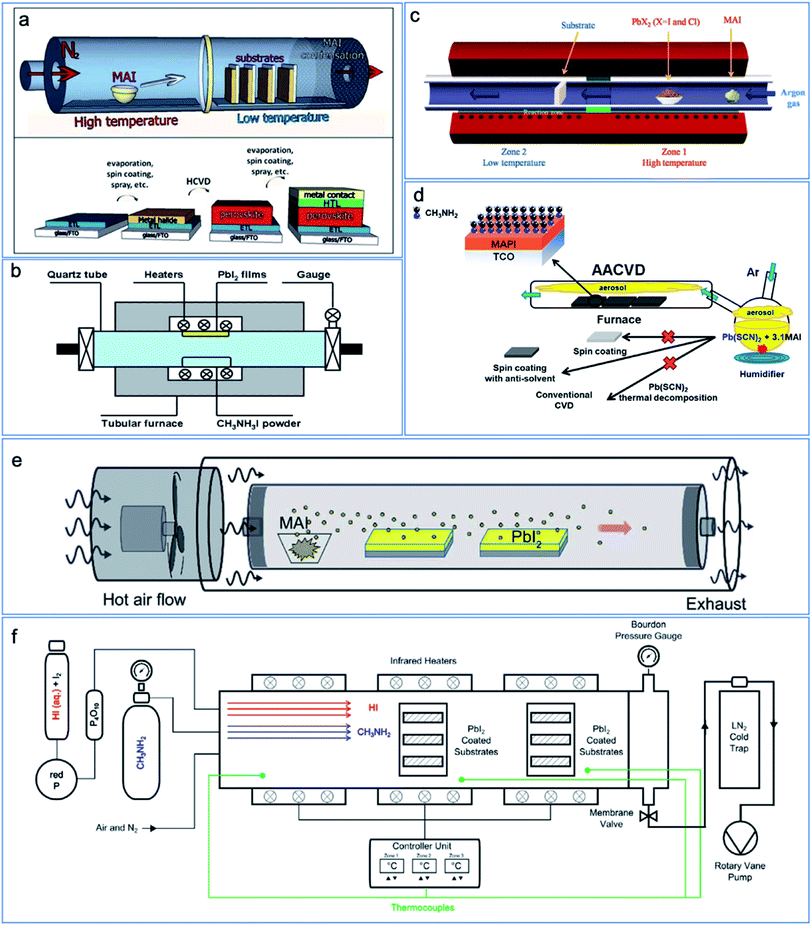 | ||
| Fig. 1 Schematic drawing showing the various types of modified CVD to prepare perovskite materials. (a) Double-zone HCVD process.8 Published by The Royal Society of Chemistry. (b) Single-zone HCVD process. Reproduced from ref. 24 with permission from The Royal Society of Chemistry. (c) One-step HCVD process. Reproduced from ref. 25 with permission from Springer Nature. (d) Ambient pressure AACVD process. Reproduced with permission from ref. 26. Copyright 2019 American Chemical Society. (e) Ambient pressure double-zone HCVD process. Reproduced from ref. 27 with permission from The Royal Society of Chemistry. (f) MA gas with HI vapor-based CVD process; reproduced from ref. 28 with permission from John Wiley & Sons. | ||
2.1 Hybrid CVD (HCVD)
| 3MAI(g) + PbCl2(s) = MAPbI3 + 2MACl(g) | (1) |
| MAI(g) + PbI2(s) = MAPbI3 | (2) |
As can be seen in Fig. 1a, there are two zones for the HCVD process, with one zone dedicated for the sublimation of organic halide precursor and the other zone for the sublimed organic halide precursor to react with the substrates that have been already pre-deposited with lead halide. In this case, the temperatures of each zone can be independently controlled. The parameters including the pressure, temperature, flowing gas and deposition time can be tuned to control the film formation. The diffusion of vapor precursor follows the relation of Dg ∝ T3/2/P (where Dg is the gas diffusion constant, T is the temperature, and P is the pressure). A balance between the condensing/diffusion of organic halide vapor and the reaction for the formation of perovskite should be considered. With a higher pressure and temperature in the organic precursor loaded zone, there will be a higher organic precursor vapor pressure. On the other hand, a higher organic precursor vapor pressure leads to a faster deposition of organic precursor on the PbI2 substrate in the second zone. If the condensation of organic precursor is faster than the diffusion and reaction rate with PbI2, extra organic halide salt will be deposited, which might deteriorate the film quality. If the condensation of organic precursor is slower than the diffusion and reaction rate with PbI2, a longer time is required for the complete formation of perovskite. The diffusion and reaction rate between organic precursor and PbI2 is determined by the temperature of the PbI2 loaded zone. By controlling the temperature of the two zones and the pressure in the tube, a balance between condensing, diffusion, and reaction for the formation of high-quality perovskite can be achieved. A more detailed mechanism is introduced in the following section.
The deposition of inorganic lead precursor film can be solution coating process or a thermal evaporation process. Because the film formation process of this inorganic lead precursor film is not a limiting factor for large area and uniform deposition of perovskite, this film deposition is more flexible. With a spray-coated PbI2 as the inorganic precursor, the waste of toxic Pb could be minimized compared with vacuum deposition. Besides, a spray coating of PbI2 is suitable for large-scale deposition at a low cost. As reported, the spray-coated PbI2 combining with a double zone HCVD results in uniformity and high-quality of the deposited perovskite film. Such perovskite films, when used to prepare mini-modules, showed a PCE up to 15% with an area of 12 cm2 (Table 1).29
| Device structure | Technique for perovskite | Area (cm2) | Efficiency (%) | V OC (V) | J SC (mA cm−2) | Fill factor | Charge carrier lifetime (ns) | Lifetime (h) | Ref. |
|---|---|---|---|---|---|---|---|---|---|
| a c-TiO2: compact TiO2 layer. m-TiO2: mesoporous TiO2. b Storage stability. c Operational stability. d V OC: open-circuit voltage; JSC: short-circuit current. | |||||||||
| FTO/c-TiO2/m-TiO2/MAPbI3/spiro-MeOTAD/Au | Double zone-HCVD | 0.09 | 10.8 | 0.92 | 19.1 | 0.62 | NA | 1100b | 8 |
| FTO/c-TiO2/m-TiO2/FAPbI3−xClx/spiro-MeOTAD/Au | Double zone-HCVD | 0.09 | 14.2 | 1.03 | 20.9 | 0.66 | NA | 155 daysb | 34 |
| 1 | 7.7 | 0.97 | 18.4 | 0.43 | NA | NA | |||
| FTO/c-TiO2/MAPbI3/spiro-MeOTAD/Ag | Double-zone HCVD | 0.12 | 12.73 | 0.91 | 1.7 | 0.645 | 34 | NA | 9 |
| FTO/c-TiO2/MAPbI3−xClx/spiro-MeOTAD/Au | Single-zone HCVD | 0.062 | 16.8 | 1.04 | 21.7 | 0.75 | NA | NA | 71 |
| FTO/c-TiO2/MAPbI3/spiro-MeOTAD/Ag | Single-zone HCVD | 0.12 | 12.2 | 0.952 | 21.0 | 0.61 | NA | NA | 24 |
| FTO/c-TiO2/m-TiO2/MAPbI3/spiro-MeOTAD/Au | Single-zone HCVD | 0.16 | 14.7 | 1.05 | 22.63 | 0.60 | NA | 31 daysb | 38 |
| FTO/c-TiO2/MAPbI3/spiro-MeOTAD/Au | One-step HCVD | NA | 9.2 | 0.95 | 15.9 | 0.61 | 10 | NA | 25 |
| FTO/c-TiO2/MAPbI3−xClx/spiro-MeOTAD/Au | 11.1 | 0.97 | 18 | 0.64 | 120 | ||||
| ITO/ZnPc/MAPbI3/C60/BCP/Al | Single-zone HCVD | 0.032 | 11.6 | 0.96 | 17.26 | 0.70 | NA | NA | 30 |
| FTO/c-TiO2/m-TiO2/MAPbI3/spiro-MeOTAD/Au | Double-zone HCVD | 0.09 | 15.6 | 1.06 | 21.7 | 0.68 | NA | NA | 10 |
| FTO/c-TiO2/m-TiO2/FAPbI3/spiro-MeOTAD/Au | 2.0 | 10.4 | 1.02 | 19.5 | 0.53 | ||||
| 8.8 | 9.5 | 0.98 | 16.9 | 0.57 | |||||
| 12.0 | 9.0 | 0.94 | 17.8 | 0.54 | |||||
| FTO/c-TiO2/m-TiO2/MAPbI3/spiro-MeOTAD/Au | Double-zone HCVD | 0.06 | 17.6 | 1.00 | 23.0 | 0.77 | ∼200 | NA | 31 |
| FTO/c-TiO2/m-TiO2/MAPbI3/spiro-MeOTAD/Au | MA gas + HI vapor | 0.09 | 15.3 | 1.05 | 20.6 | 0.71 | NA | 133 daysb | 55 |
| FTO/c-TiO2/m-TiO2/MAPbI3/spiro-MeOTAD/Au | Single-zone HCVD | 0.24 | 14.99 | 1.04 | 19.19 | 0.74 | NA | NA | 72 |
| FTO/c-TiO2/MAPbI3/spiro-MeOTAD/Au | 0.24 | 15.37 | 0.972 | 21.15 | 0.75 | ||||
| FTO/c-TiO2/m-TiO2/MAPbI3/spiro-MeOTAD/Au | 8.4 | 6.22 | 2.93 | 3.43 | 0.61 | ||||
| FTO/c-TiO2/m-TiO2/MAPbI3/spiro-MeOTAD/Au | Double-zone HCVD (ambient pressure) | 0.11 | 18.90 | 1.06 | 22.08 | 0.80 | NA | NA | 27 |
| ITO/PTAA/MAPbI3/PCBM/ZnO/Al | Double-zone HCVD | NA | 15.4 | 0.955 | 22.7 | 71.0 | 2.4 | NA | 73 |
| FTO/c-TiO2/m-TiO2/Cs0.15FA0.85PbI3/spiro-MeOTAD/Ag | Single-zone HCVD | 0.12 | 14.45 | 0.906 | 22.858 | 0.698 | NA | 7 daysb | 43 |
| FTO/c-TiO2/MAPbI3−xClx/spiro-MeOTAD/Au | Single-zone HCVD | 0.09 | 11.5 | 0.91 | 18.33 | 0.67 | NA | NA | 74 |
| FTO/c-TiO2/m-TiO2/Cs0.07FA0.93PbI3/spiro-MeOTAD/Au | Double-zone HCVD | 0.1 | 16.6 | 1.00 | 22.00 | 0.752 | NA | 20c | 75 |
| 12.0 | 14.6 | 5.84 | 3.67 | 0.681 | NA | ||||
| FTO/c-TiO2/m-TiO2/(PEA2MAn−1PbnI3n+1)/spiro-MeOTAD/Au | Single-zone HCVD | 0.2 | 19.10 | 1.08 | 21.91 | 0.8036 | NA | 67 | |
| FTO/SnO2/Cs0.24FA0.76PbI3−yBry/spiro-MeOTAD/Au | Single-zone HCVD | 0.16 | 17.79 | 1.065 | 22.88 | 0.712 | ∼300 | NA | 40 |
| 41.25 | 12.24 | 9.16 | 2.25 | 0.526 | |||||
| FTO/c-TiO2/CsPbBr3/carbon | Single-zone HCVD | 0.12 | 5.38 | 1.13 | 6.79 | 0.70 | NA | 21 daysb | 76 |
| FTO/c-TiO2/m-TiO2/MAPbI3/spiro-MeOTAD/Au | Double-zone HCVD | 0.06 | 16.9 | 1.01 | 24.2 | 0.69 | NA | NA | 77 |
| FTO/c-TiO2/Cs0.15FA0.85PbI2.85Br0.15/spiro-MeOTAD/Au | Single-zone HCVD | 0.09 | 18.22 | 1.06 | 22.82 | 0.754 | NA | 1400b | 42 |
| FTO/c-TiO2/MAPbI3/SWCNT | Single-zone HCVD | NA | 7.9 | 0.91 | 15.5 | 0.56 | NA | 500b | 78 |
| FTO/c-TiO2/MAPbI3/spiro-MeOTAD/Au | Single-zone HCVD | 0.09 | 15.5 | 1.03 | 20.46 | 0.73 | NA | NA | 66 |
| FTO/c-TiO2/Cs0.1FA0.9PbI3/spiro-MeOTAD/Au | Single-zone HCVD | NA | 16.39 | 0.99 | 22.87 | 0.7482 | 21 | 30 days | 79 |
| Ti/c-TiO2/m-TiO2/FAPbI3−xClx/spiro-MeOTAD/Au | Single-zone HCVD | 0.05 | 10.79 | 0.95 | 15.14 | 0.75 | NA | NA | 80 |
| FTO/c-TiO2/m-TiO2/FAPbIxBr3−x/spiro-MeOTAD/Au | Double-zone HCVD | 0.1 | 16.2 | 1.03 | 21.1 | 0.74 | NA | 535c | 29 |
| 2.0 | 16.1 | 1.03 | 21.1 | 0.74 | NA | ||||
| 12.0 | 14.7 | 6.29 | 3.55 | 0.66 | 388c | ||||
| FTO/SnO2/C60/Cs0.1FA0.9PbI2.9Br0.1/spiro-MeOTAD/Au | Double-zone HCVD | 0.09 | 13.3 | 0.90 | 20.2 | 0.67 | 40 | 500c | 16 |
| 91.8 | 9.34 | 13.55 | 1.16 | 0.596 | |||||
| FTO/c-TiO2/m-TiO2/MABiI3/spiro-MeOTAD/Au | CVD | 0.19 | 0.02 | 0.39 | 0.13 | 0.3896 | NA | NA | 81 |
| FTO/c-TiO2/PCBM/MAPbI3/spiro-MeOTAD/Au | Single-zone HCVD | 0.09 | 12.2 | 0.922 | 18.7 | 0.71 | NA | NA | 82 |
| FTO/SnO2/Cs0.24FA0.76PbI3−yBry(SrI)/spiro-MeOTAD/Au | Single-zone HCVD | 0.16 | 17.66 | 1.021 | 21.96 | 0.789 | NA | 60 daysb | 44 |
| 16.07 | 13.92 | 6.280 | 3.29 | 0.674 | NA | NA | |||
| FTO/c-TiO2/C60/(PEA2MAn−1PbnI3n+1)/spiro-MeOTAD/Au | Single-zone HCVD | NA | 18.08 | 1.08 | 23.75 | 0.704 | NA | 30 daysb | 68 |
| FTO/c-TiO2/m-TiO2/MAPbI3/spiro-MeOTAD/Au | MA gas + HI vapor | 0.325 | 12.9 | 1.04 | 18.6 | 0.67 | NA | NA | 28 |
| ITO/PTAA/Cs0.24FA0.76PbI3−yBry/ZnO/AZO/Ni–Al-grid | Double zone HCVD | 0.27 | 10.6 | 0.95 | 17.5 | 0.6 | 55 | NA | 60 |
| FTO/SnO2/Cs0.1FA0.9PbI3/spiro-MeOTAD/Au | Double zone HCVD | 0.1 | 15.5 | 0.99 | 22.3 | 0.702 | NA | NA | 17 |
| 22.4 | 12.3 | 6.8 | 2.7 | 0.672 | |||||
| FTO/SnO2/Rb0.04Cs0.14FA0.86Pb(BryI1−y)3/spiro-MeOTAD/Au | Single zone HCVD | 0.148 | 19.59 | 1.127 | 22.63 | 0.768 | ∼270 | NA | 36 |
| 10.0 | 15.13 | 6.243 | 3.51 | 0.70 | |||||
| FTO/SnO2/Rb0.04Cs0.14FA0.86Pb(BrxI1−x)3/spiro-MeOTAD/Au | Single zone HCVD | 0.16 | 19.6 | 1.13 | 22.20 | 0.78 | ∼150 | NA | 65 |
In a fully vapor-based deposition process, the morphology of PbI2 determines the quality of deposited perovskite films, which can be affected by the deposition rate,30 the carrier gas and the environment.9,31 Deposition rates of 3.5, 4.5 and 5.2 Å s−1 were investigated and it was found that with a higher deposition rate, the deposited PbI2 film showed a higher degree of orientation along the (001) planes, in parallel to the substrates. Such a textured PbI2 film is beneficial for MAI vapor intercalation. A higher deposition rate also resulted in smaller PbI2 grains and a smoother surface.30 While a lower deposition rate below 1 Å s−1 is expected for a compact and smooth film,8,16 as it is applied in most reported works, a higher deposition rate might further improve the device performance.30 Besides the deposition rate, the carrier gas of HCVD can be ambient air with a low vacuum, as shown in Fig. 2.9 As reported, a post-annealing treatment is required for the complete formation of high-quality MAPbI3.9
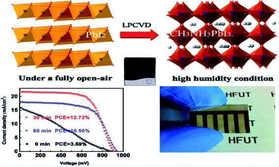 | ||
| Fig. 2 Double zone HCVD with humid air as carrier gas. A post-annealing process is required for high-performance perovskite solar cells. Reprinted with permission from ref. 9. Copyright 2015 American Chemical Society. | ||
The compositions of perovskite are versatile in HCVD. Because MA-based perovskite is not stable under high temperature, CH(NH2)2 (FA) based perovskite has been intensively studied in recent years. With the replacement of MA with FA, the bandgap is reduced approaching the optimal value for single-junction solar cells. Recently pure FA-based perovskite solar cells have shown certified efficiency of 25.2%.32,33 HCVD has also been used for fabricating large area FA-based perovskite solar cells.34,35 The sublimation of FAI vapor and the reaction between the FAI and PbI2/PbCl2 is crucial for forming a stoichiometric FAPbI3 film (eqn (3) and (4)).
| FAI(g) + PbI2(s) = FAPbI3 | (3) |
| 2FAI(g) + PbCl2(s) = 2FACl(g) + PbI2 | (4) |
It is proposed that PbCl2 is a better inorganic precursor than PbI2, because Cl is smaller and allows for easier halide exchange.36 In addition, the presence of Cl can help improve the film quality. However, it is hard to control the stoichiometry of perovskite films with vapor deposition of the organic component. The substrate loaded at different positions of the double zone furnace has different temperatures due to the temperature gradient, and the amount of deposited FAI also varies.34 The under-saturation and over-saturation reactions happen in the near high-temperature side and near low-temperature side, respectively. Thus, precise control of deposition time and the substrate position is required. Both under-saturation and over-saturation conditions decrease the device performance. In the case of over-saturation conditions, although the prolonged annealing process can re-sublimate the over-saturated organic component and it is a reversible process, the grain size gets smaller.34 Low-pressure vapor deposition gives precise control in film thickness and microstructure. But problems arise in controlling the stoichiometry of the inorganic–organic components as PbI2 often remains in the resulting films.37
Tuning the inorganic precursor composition is an alternative strategy for perovskite composition adjusting. Considering that the Cs–FA double cation perovskite is promising for high performance, phase stable and thermal stable solar cells, co-evaporation of CsBr/PbI2 at the first stage has been reported.16 In the second step with the deposition of FAI, a mixed cation, mixed halide perovskite Cs0.1FA0.9PbI2.9Br0.1 with a large area was obtained (Fig. 3). This is the largest reported perovskite solar module fabricated by HCVD so far (Fig. 3a and b). The area can be readily scaled up with a larger furnace tube.
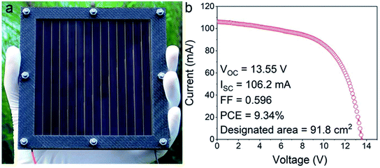 | ||
| Fig. 3 (a) An optical photograph and (b) I–V curves of a HCVD deposited perovskite solar module on a 100 cm2 substrate with a designated area of 91.8 cm2.16 Published by The Royal Society of Chemistry. | ||
A tubular furnace with a single zone for CVD was applied for the deposition of MAPbI3 (Fig. 1b). Similarly, the closed space sublimation can be considered as single zone CVD. A CsMAPbI3 with efficiency approaching 20% has been achieved with the closed space sublimation by putting CsCl/PbCl2 above an MAI thin film under controlled temperature.41 Tong et al. converted a sequentially evaporated CsBr/PbI2 stack with FAI for 100 minutes at 140 °C to realize a compositionally graded absorber and achieved an opaque device with a PCE of 18.2% (0.09 cm2).42 The mixed inorganic cation species can also be introduced in the first step by a solution coating of CsI/PbI2.43 Recently, with a homemade chamber, the mixed cation, mixed halide perovskite has been reported with the single zone CVD, which showed an efficiency up to 19.6%, which is currently the highest PCE for perovskite solar cells by CVD.36,44
2.2 One-step CVD
A one-step CVD has been developed for the fabrication of perovskite layers (Fig. 1c).25 The one-step CVD is similar to one-step co-evaporation, but in a low vacuum and at a low cost. Due to the low vacuum condition, a higher temperature is required for material sublimation and vapor transport. As shown in Fig. 1c, the schematic drawing shows the furnace for the one-step CVD. A high temperature for PbI2 or PbCl2 is required in the first zone. In the upstream before the high-temperature zone, the organic precursor (i.e., MAI) is loaded in a lower temperature region. Subsequently, carrying with argon gas, the PbI2/PbCl2 and MAI vapor transport to the substrate in the downstream and form the perovskite.25 For the formation of perovskite, after the deposition of inorganic and organic vapor, the substrate was annealed in situ in the second zone for the complete conversion. Comparing PbI2 with PbCl2 precursor, it is found that the presence of Cl helps minimize the morphological and energetic disorder of the deposited film. The presence of Cl is detected in the perovskite film, which accounts for a longer carrier lifetime (Table 1).25 The highest efficiency of 11.1% has been obtained by this one-step CVD. This one-step CVD is also suitable for other compositions by selecting the precursor and controlling the temperature and pressure. For example, MA3Bi2I9 (ref. 45) and CsPbBr3 (ref. 46) have been reported by one-step CVD. For the MA3Bi2I9 and CsPbBr3, the sublimation temperature of the precursor is similar, thus the precursor powder can be put in more close positions.2.3 Ambient pressure CVD
The ambient pressure CVD can be referred to as aerosol-assisted chemical vapor deposition (AACVD) and ambient pressure HCVD.13,27 AACVD is an ambient-pressure CVD technique in which that via nebulization of precursor molecules, the aerosol is transported by an inert carrier gas such as argon or nitrogen to a substrate surface (Fig. 1d).26 Similar to spray coating, AACVD also requires the ultrasonic vaporization of the solution and formation of mist. AACVD can be a one-step or two-step process. The one-step AACVD is to deposit the perovskite precursor with the carrier gas.26 The two-step deposition is to deposit PbI2 or PbBr2 by either vapor or solution coating in the first step13 and to react with the mist mainly consisting of the organic halide precursor, e.g., MAI, MABr, FAI, etc. in the second step. In this way, the composition can be readily controlled by changing the organic halide precursor solution and the deposition takes place at a relatively low temperature. Various perovskites have been successfully deposited on glass or FTO/TiO2 substrates, including MAPbBr3,13 MAPbI3,26,37,47–49 MAPb(Br1−xClx)3,50 CsPbBr2I,51 bromine doped MAPbI3,52 and double perovskite Cs2SnI6 (ref. 53) by AACVD. Although AACVD has been developed in the early stage for the deposition of perovskite film, to our best knowledge, none of the deposited perovskite films has been incorporated into a working solar cell device.Another reported ambient pressure CVD for the deposition of MAPbI3 is schematically shown in Fig. 1e.27 The vaporization of MAI is induced by hot air at a temperature of 180 °C and with a humidity of 10%. The diffusion of MAI vapor happens from the surface to the bottom, thus the morphology of the PbI2 film significantly influences the perovskite film quality, as shown in Fig. 4a. A mesoporous PbI2 is beneficial for MAI vapor diffusion and a larger grain size is obtained compared with conventional compact PbI2 (Fig. 4b and c). The perovskite layer prepared using mesoporous PbI2 is also of higher quality, which showed a high PCE up to 18.90% with an active area of 0.1 cm2.27 The mesoporous PbI2 can be deposited by adding dimethyl sulfoxide (DMSO) into the PbI2 precursor solution, which is better for formation of amorphous PbI2 and MAI vapor diffusion.54 However, the process might not be suitable for FAPbI3 perovskite due to its sensitivity to moisture.
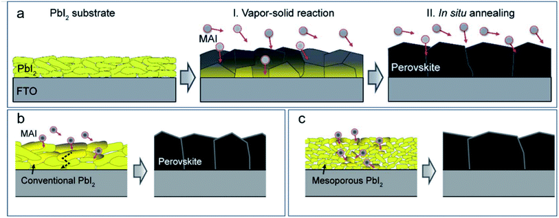 | ||
| Fig. 4 (a) Perovskite formation mechanism with MAI vapor diffusing into PbI2. Effect of (b) compact PbI2 and (c) mesoporous PbI2 on the formation of perovskite. Reproduced from ref. 27 with permission from The Royal Society of Chemistry. | ||
2.4 CVD of perovskite with CH3NH2 gas and HI vapor
The perovskite can be formed by a rapid reaction between PbI2 and CH3NH2 vapor with the assistance of moisture in ambient air or in a tube furnace in a low vacuum.55 A systematic study and schematic drawing showing the reaction and formation of perovskite are depicted in Fig. 5. The reaction happens rapidly in a few seconds. The volatile and excess MA gas leaves the film, and results in a final mirror-like smooth film consists of MAPbI3 perovskite and byproducts such as PbO and Pb(OH)2. The byproducts can be reduced by exposing one or multiple cycles of HI vapor exposure and MA vapor exposure, which can lead to higher performance in perovskite solar cells. The highest efficiency reaching 15.3% was obtained.55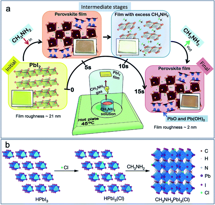 | ||
| Fig. 5 Schematic drawing showing the formation of perovskite by the reaction between (a) PbI2 and MA gas (with the assistance of moisture in ambient air).55 Published by The Royal Society of Chemistry. (b) HPbI3 and MA gas. Reproduced from ref. 56 with permission from Springer Nature. | ||
A modified CVD process has been designed recently based on the above-mentioned research, and the scheme of the tube furnace set-up for purging MA gas and HI vapor is shown in Fig. 1f.28 Considering the mechanism for the formation of perovskite by this method, a suitable humid air is required as the carrier gas. Between the purging of MA gas and HI vapor, a vacuum pumping process is applied. A PCE of 11.7% has been obtained by this CVD setup. Although the remaining PbO and Pb(OH)2 in the film could not be detected by X-ray diffraction (XRD), the X-ray photoelectron spectroscopy (XPS) measurement showed that these species were present at least on the surface of the final film.28 The purging with MA gas and HI vapor at the same time might help reduce the amount of byproducts. However, the reaction between MA gas and HI vapor for the formation of MAI is too fast to be precisely controlled before inserting the PbI2 layer.55
To eliminate the byproducts, an alternative strategy is to apply HPbI3 as a precursor instead of PbI2.57 The reaction between HPbI3 and MA gas can form stoichiometric MAPbI3 thin films, as shown in Fig. 5b.56 The highly volatile MA gas can easily diffuse into HPbI3 for the formation of high quality and thick perovskite films. The presence of Cl can further improve the film quality at a film thickness up to 1.2 μm. The longest carrier lifetime of 500 ns is reported by this vapor–solid reaction process. PCEs of 21% for small area solar cell (0.1 cm2) and 15.3% for the solar module (12 cm2 active area) were obtained. More importantly, the high-quality thick film is promising for high operational stability, and the perovskite solar cell maintained 90% of its initial performance after continuous AM 1.5G illumination over 2000 h.56
2.5 CVD growth of perovskite single crystals
High quality perovskite films have been demonstrated by the above-summarized CVD processes. Furthermore, these CVD processes can deposit perovskite single crystals with elaborate modifications.14,58,59 A HCVD has been applied with MAI deposition on vacuum deposited PbI2 platelets (Fig. 6a). The conversion happens with the insertion of MAI into the PbI2 crystal structure accompanied by an expansion of volume and formation of platelets such as single crystals (Fig. 6b–d). The diffusion length of electrons in the HCVD deposited single crystals is up to 210 nm, which is beneficial for optoelectronic applications such as light-emitting diodes and lasers.14 A wet chemical and AACVD process has been applied for the synthesis of perovskite CsPbIBr2 nanosquares and deposition onto glass substrates.51 The single crystalline nano/micro-platelet perovskite can also be deposited by the one-step CVD process.58 The size of the platelets can be tuned by adjusting the PbI2 platelets/powder, MAI powder, substrate deposition location, temperature and time in the HCVD process.59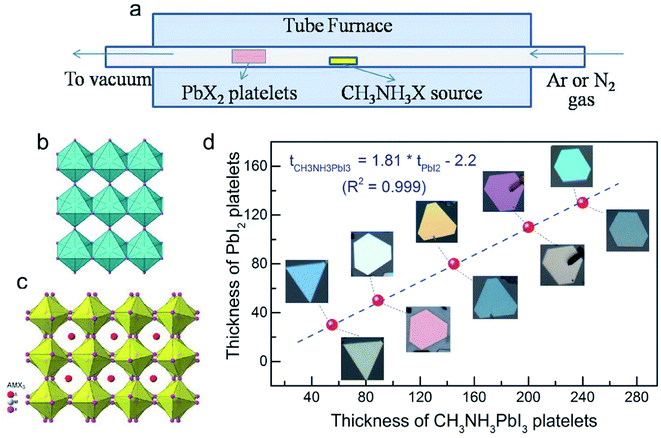 | ||
| Fig. 6 (a) Schematical drawing showing the CVD deposition of perovskite single crystals with PbX2 platelets as the precursor. (b) Structure of PbX2 platelets. (c) Structure of perovskite with the insertion of the organic halide into the crystal structure of PbX2. (d) The thickness of as-deposited perovskite platelets as a function of the thickness of PbI2 platelets precursors. Reproduced from ref. 14 with permission from Jon Wiley and Sons. | ||
2.6 Formation kinetics of modified CVD deposited perovskite
Although various modified CVD techniques have been introduced in the previous section, the underlying principle is similar, i.e., the sublimation or vaporization of organic vapor and the transport of the vapor to the substrate pre-deposited with the inorganic precursor film. Recently the isothermal CVD process for the perovskite layers has been studied with a dual-direction pumping system. In this system, the influence of the sublimated FAI vapor during the ramping and cooling process can be avoided and the study of the kinetics for perovskite film formation is possible. The authors experimentally confirmed that the temperature of the sources and substrate influence the reaction stage. There is a balance between the FAI vapor deposition amount and the reaction rate with the bottom PbI2.60Regarding the overshoot during the ramping process and the over-saturation of organic vapor, a rapid and precise heating and cooling process is required.17 By switching the pumping direction and correspondingly changing the organic vapor flow direction, the reaction kinetics between the vapor–solid has been systematically studied (Fig. 7a and b).60 In this case, both ends of the furnace tube are connected to the carrier gas supply and pump, which is flexibly switched. Before reaching the stable temperature, the organic vapor is purged out directly with a carrier gas, without passing through PbI2 substrate. By switching the vapor gas flow direction, the deposition of organic halide and conversion to perovskite takes place. With a precise controlling of deposition time, the gas flow is switched to a reverse direction again to prevent excess organic vapor deposition, which is beneficial for stoichiometric perovskite formation. Furthermore, the conversion kinetics of the hybrid CVD can be studied for each deposition step (Fig. 7c and d).
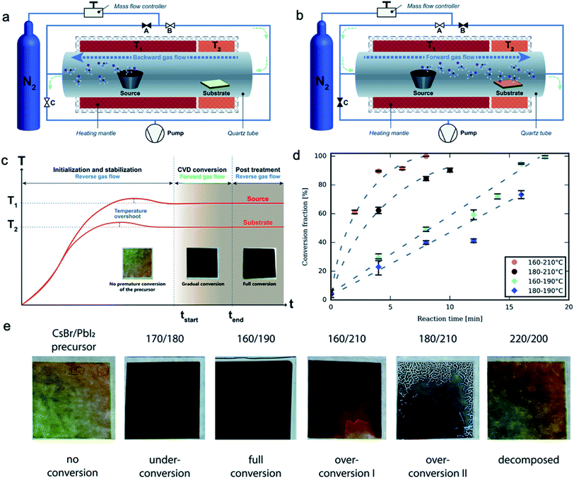 | ||
| Fig. 7 Schematic drawing showing the organic vapor gas flow direction during (a) ramping and cooling process, and (b) perovskite growing process. (c) Temperature profile during the HCVD process. (d) Perovskite growth kinetics with combinations of different two-zone temperatures. (e) The conversion stages of perovskite with different temperature combinations. Reproduced from ref. 60 with permission from The Royal Society of Chemistry. | ||
The conversion of the perovskite can be stopped at any time by switching the vapor gas flow to a reverse direction (Fig. 7c). The reaction progress or reaction fraction can be controlled by the reversing of gas flow direction. The reaction rate is affected by the temperature of organic sources and the temperature of substrates, as shown in Fig. 7d. A combination of the two temperatures balances the transport of organic vapor and the deposition and reaction of the FAI vapor and the CsBr/PbI2 substrate. A 250 nm-thick CsBr/PbI2 film fully converted to a high-quality perovskite within a short time of 8 min, as shown in Fig. 7c. This is considerably short compared with the reported total process time, which includes 1 to 3 hours of annealing. The much longer process time in total is due to the slow thermal response and ramping rate, and a long thermal equilibrium time. If we only consider the reaction time, CVD is a relatively fast technique for depositing perovskite films.60 A higher temperature of the organic source increases the reaction rate, which is due to a higher sublimation of organic vapor and faster transport to the substrate. However, a higher temperature of the substrate not always results in a higher reaction rate. This is limited by the deposition of the organic vapor and the diffusion of this organic vapor into the CsBr/PbI2 layers (Fig. 7e). This study shows a clear clue for the design of CVD setup for high quality and uniform perovskite layers. As proof of concept semi-transparent perovskite solar cell with 9.7% has been obtained without any post-treatment process.
2.7 Scalability of modified CVD for fabricating perovskite solar cells/modules
One of the most promising advantages of vapor deposition is scalability. As summarized in several review articles, the currently reported perovskite solar cells show markedly decreased performance with increasing area, compared with other mature photovoltaic techniques.3,6 The main reason is that film uniformity can not be preserved when increasing from small to large area. Modified CVD can potentially address this issue. When HCVD is used to fabricate perovskite solar modules, as the area increases from 0.1 cm2 (13.4% PCE) to 91.8 cm2 (designated area, 9.3% PCE) the efficiency decay rate is 1.3% per decade area (Fig. 8). This decay slope is similar to other mature photovoltaic techniques (in the range 0.8–1.0% per decade area).6 It is worth noting so far the cell and module efficiencies are still lower than solution-processed devices. One of the main limitations comes from the poor quality of the electron transport layer (ETL) after a long time of vacuum annealing inside a tube furnace.16,17,61 This vacuum annealing process increases the density of gap states above the valence band of the ETL and increases interface charge recombination, which deteriorates the device performance.16,17 The vacuum annealing process will take away some oxygen from SnO2 surface and deteriorates its optical/electronic properties, which forms the gap states and decreases the junction performance in solar cells.62 These gap states are associated with Sn-5s electrons that become occupied as the surface reduces to form a Sn2+ surface layer.61,63 With reduced vacuum deposition time, the cells (15.1% for 0.1 cm2) and modules (12.3% for 22.4 cm2 designated area) efficiencies both increased, although still are not comparable with the solution processed devices yet.17,64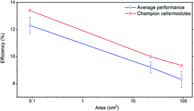 | ||
| Fig. 8 Solar cell efficiency decays as a function of cell/module designate area with both champion and average solar cells/modules performance.16 Published by The Royal Society of Chemistry. | ||
3. Rapid HCVD of perovskite films
Because the vacuum annealing process might deteriorate the quality of charge transport layer, reduced vacuum annealing time can be beneficial. To reduce the vacuum annealing time, one needs to consider the thermal transfer processing time and annealing processing time. A possible alternative is to change the conventional heating element of filament to infrared radiation heating. The rapid thermal process has been recently developed by Qi and coworkers.17 The ultra-fast ramping and deposition has been obtained and the CVD time has been reduced from 2–3 hours to 10 min, which is on the same order with the above-mentioned study on the HCVD kinetics.60Fig. 9a shows the schematic drawing of the rapid HCVD for high-quality perovskite films, with rapid ramping, efficient annealing, and cooling, by infrared radiation and moving of heating element. In this system, the quality of electron transport layer has been better maintained, with fewer band-gap states above the valence band and hence higher electron mobility. The solar cell/module performance has been improved accordingly.17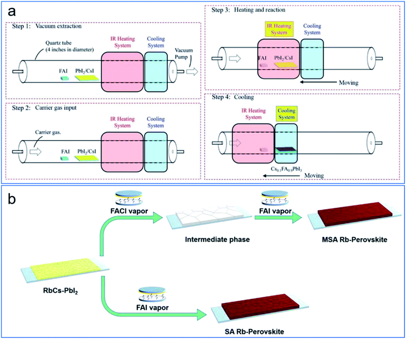 | ||
| Fig. 9 (a) Schematic drawing showing the steps of rapid HCVD for perovskite films.17 Published by The Royal Society of Chemistry. (b) Rapid formation of high-quality perovskite films with fast halide anion exchange process. Reprinted from ref. 36 with permission from Elsevier. | ||
Another consideration for increasing the gas–solid reaction and reduction of deposition time is from the fast halide anion exchange.36,65 It has been reported that, with a smaller radius, chloride moves faster than iodide in a gas–solid reaction process. On the other hand, when exposed to an iodide environment, the rapid exchange between chloride and iodide happens. As shown in Fig. 9b, with a two-step deposition, and the formation of an intermediate phase by deposition of FACl in the first step, the formation of perovskite was much faster.36 The second step for the formation of perovskite was around 5 min. This process was used to fabricate perovskite solar cells, and an efficiency up to 19.6% was obtained (0.16 cm2). Addition of FACl with FAI in the organic vapor also improved the quality of perovskite layer and the module performance. By incorporation of FACl, perovskite solar modules with efficiencies of 15% (active area of 12 cm2),29 and 12.24% (active area of 41.25 cm2)40 have been obtained.
4. Factors influencing the perovskite layer quality and device performance
Based on the above discussion, to fabricate high-quality perovskite thin films via these modified CVD methods, several factors should be taken into account: the inorganic layer morphology and composition, the thickness of the inorganic layer, the organic vapor, and the carrier gas for organic vapor.4.1 Morphology and composition of the inorganic layer
For vacuum deposited PbI2, the deposition rate of PbI2 influences the crystal orientation and morphology. As discussed in Section 2, a higher deposition rate results in higher device performance.30 On the other hand, for a solution coated PbI2 film, the solvent component also influences the resulting film morphology and crystallinity. For example, by adding DMSO into the solution, a porous and amorphous PbI2 film was obtained, which was beneficial for gas vapor infiltration and larger perovskite grains.27 This PbI2 precursor solution with DMSO is applied to a spray coating technique, which was used to fabricate perovskite solar modules with negligible Pb waste.29 Addition of CsI or CsBr into the PbI2 layer can help improve the phase stability of the resulting film.16,17,43 The layer thickness of the perovskite is determined by the complete reaction of the inorganic layer, due to a diffusion barrier.8,34,66Recently RbI, SrI2, and KI have been added into the PbI2 inorganic layer to tune the composition of the resulting film.36,44,65 On the other hand, a gradient composition can be formed by deposition of the CsBr/PbBr2 inorganic layer with the FAI organic vapor (Fig. 10a).16,17,42,60 In this case, by using sequentially deposited CsBr and PbBr2 as inorganic layer and FAI as the organic vapor source, a high quality and gradient composition perovskite film was fabricated. The resulting film consists of mainly I− as anion and the result devices showed an efficiency of 18%.42 By adding the RbI, SrI, and KI into the PbI2, the Br anion could be stabilized during the halide exchange with FAI vapor. Mixed cation, mixed halide perovskite Cs0.14FA0.86Pb(BrxI1−x)3 has been obtained with Rb, Sr or K doping. The device efficiency was up to 19.6% (Fig. 10b).36,44,65 The use of FACl to form an intermedia accelerated the halogen exchange and perovskite formation, which may help reduce the defect density in the bulk. As a result, small area cells with an efficiency of up to 19.6% have been reported.36 This method was further applied for the fabrication of large-area modules of 16.07 cm2, which demonstrate an efficiency of 13.9%.44 2D perovskites have been investigated due to their higher thermal and moisture stability. As a demonstration, PEAI has been added into the PbI2 layer for the following CVD of MAI. This process formed a 2D/3D mixed perovskite with high quality and the resulting device showed an efficiency of 19.10% for a small area solar cell (Fig. 10c).67,68
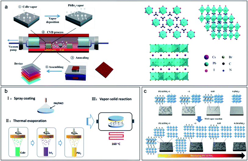 | ||
| Fig. 10 (a) Schematic drawing showing a sequential deposition of CsBr/PbBr2 and CVD of FAI for high quality perovskite films and devices. Reprinted from ref. 42 with permission from Elsevier. (b) Mixed halide perovskite stabilized by SrI2 doping and CVD deposition of FAI/FACl. Reproduced from ref. 44 with permission from The Royal Society of Chemistry. (c) 2D/3D perovskite deposited by the CVD process of MAI reacting with PbI2/PEAI. Reproduced from ref. 67 with permission from John Wiley and Sons. | ||
4.2 Carrier gas and deposition environment
Either in a low or ambient pressure, the carrier gas is an important component transporting the organic vapor to the reaction zone.69 In most of the reported works, an inert gas such as N2 or Ar has been applied as the carrier gas.8,34 Some of the processes used humid air as the carrier gas.9,27 However, in the early stage, how the carrier gas might influence the film quality was not addressed. Mimicking dry air, a carrier gas with N2/O2 (85%/15%) has been applied and compared with N2. It was demonstrated that the high-temperature HCVD process conducted in a condition of N2/O2 (85%/15%) with a slow postdeposition cooling rate can successfully reduce the density of both the shallow and the deep level traps in MAPbI3, compared with a pure N2 environment (Fig. 11a).31 A champion device with 17.6% has been achieved with the careful control of defect density and the CVD process. However, the effect of moisture and oxygen is not clear yet, although there is a study proposing that moisture and oxygen cause more defects inside the perovskite layer (Section 5).70 At present, there are still different opinions regarding how the carrier gas and environment influence the film quality and defect density. Further studies will be required to clarify such effects.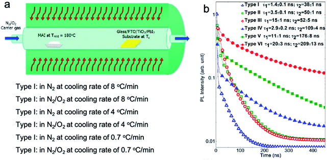 | ||
| Fig. 11 (a) Schematic drawing showing a HCVD and postdeposition annealing process under different carrier gas conditions and cooling rates. (b) Charge carrier lifetime of the perovskite films deposited in different carrier gas conditions and postdeposition cooling rates. Reprinted with permission from ref. 31. Copyright 2016 American Chemical Society. | ||
5. Difference between modified CVD deposited perovskite films and solution coated perovskite films
Although modified CVD has the potential for scalable fabrication of perovskite solar modules, the device efficiency still lags behind those based on the solution processes. Understanding the differences between solution-coated and CVD fabricated perovskite films is important for the development of CVD based large-scale and high-performance modules. So far only a few reports focus on the film properties by CVD and solution coating processes.77 Recently, the film quality and stability based on different coating techniques have been studied systematically. As shown in Fig. 12a, there are five coating processes for MAPbI3 considering the coating techniques and environment.70 It is found that a full vacuum process and CVD process in an inert N2 environment showed the most stable films under continuous light illumination. The films fabricated in air or other two-step methods showed a fast degradation rate under light illumination.70 The steady-state photoluminescence (PL) spectra also showed the highest intensity for the CVD based film (Fig. 12b). By varying the laser power for the steady-state PL measurement, the slope of the PL intensity as a function of laser power provides the information regarding the defect states inside the coated films (Fig. 12c). A slope close to 2 means that both negative and positive charge carriers are trapped. With a slope close to 1.5, either holes or electrons are trapped. A slope close to 1 indicates exclusive free carrier recombination and thus a very small number of defects and traps.83 The authors claimed that the fabrication in an inert environment could reduce the defect states, as shown in Fig. 12d.70 The CVD based process showed the most stable perovskite films,84 which is consistent with previous reports.8,9 For FAPbI3, the film also showed higher phase stability under a humid environment.34 However, this cannot explain why the performance of the device based on HCVD is lower than the solution-based methods.10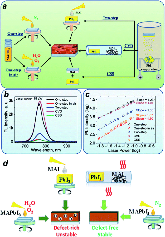 | ||
| Fig. 12 (a) Schematic drawing showing the various deposition processes for depositing perovskite films. (b) PL spectra of perovskite films deposited by various methods. (c) PL intensity of perovskite films deposited by various methods as a function of laser power. (d) Schematic drawing showing the defects inside perovskite films deposited by various methods. Reprinted with permission from ref. 70. Copyright 2020 American Chemical Society. | ||
On the other hand, by summarizing the data in Table 1, we can hypothesize that one of the main differences between solution-coated and modified CVD deposited perovskite films may be the crystal quality, which leads to different carrier lifetimes. The much shorter lifetime of CVD deposited films causes a lower open-circuit voltage.4 It can be seen that CVD deposited perovskite layer has a typical carrier lifetime in the range of 10 to 100 ns, which is shorter than solution-coated perovskite films. Table 1 summarizes the perovskite solar cells based on CVD techniques. The related photovoltaic parameters and perovskite film carrier lifetimes have also been listed. We can see that the carrier lifetime and open-circuit voltage (VOC) are relatively low compared with other reported solution-coated films. Based on the carrier lifetime, the maximum open-circuit voltage can be calculated. For example, a Cs0.1FA0.9PbI2.9Br0.1 perovskite with 40 ns lifetime has a maximum VOC of 1.04 V (Fig. 13).16 As a comparison, a solution-coated perovskite layer, the carrier lifetime can be up to 500 ns.85
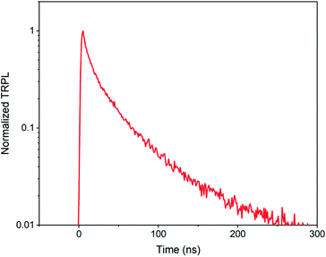 | ||
| Fig. 13 A typical time-resolved photoluminescence (TRPL) spectrum for an HCVD deposited perovskite with a carrier lifetime around 40 ns.16 Published by The Royal Society of Chemistry. | ||
Controversially to the higher stability with fewer defects in CVD deposited films, the shorter lifetime of carriers might be a result of the defects inside the bulk, instead of the defects at the grain boundaries. Such bulk defects may be the consequence of vapor deposition of precursors and/or the slow reaction rate between the gas and solid phase.60 However, for the one-step solution coating process, the precursor is a colloid of small crystals in the solvent.86 The crystal growth process is based on the nucleus, forming a high-quality grain inside the bulk with some defects around the boundaries. For the two-step solution coating process, the solvent and the ionized cations and anions might help the diffusion and reaction process, as shown in Fig. 12. We hypothesize that there might be a small amount of PbI2 that does not fully convert into perovskite during CVD process. The unreacted PbI2 can stay inside the bulk, instead of at the grain boundaries, therefore may not be detected easily by XPS. Further research is needed to verify this point.
The other obvious difference between CVD-deposited and solution-coated films is the light absorbance. It has been observed that with the same film thickness, the CVD-deposited film is more transparent than the solution-coated film. The surface of the solution-coated film is also more mirror-like. Although there is no systematic research addressing this issue yet, we hypothesize that the reasons might be related to the surface morphology and grain size, and compactness. A more compact and smoother layer can be deposited using solution-based methods, which leads to mirror-like film surfaces.70
6. Modified CVD on textured surfaces for tandem solar cells
Efficiency is one of the most important factors for a solar cell or solar module. By constructing tandem structure solar cells, PCE can be further improved over 30%.87 The application of a perovskite/Si tandem cell is the most promising strategy.88,89 In these high-performance solar cells, optical management plays a vital role and the surface structure is important. A textured structure improves light harvesting. However, it is usually challenging to use traditional solution methods to coat a perovskite film on the textured surface.89,90Via coating a thick film on the textured Si substrate by a solution process, the textured structure is smoothened and maintains part of the anti-reflection properties.90 It is reported that with a fully textured structure tandem solar cell, in which the perovskite was conformally deposited by a vacuum deposited PbI2/CsBr and solution coated FAI/MAI, the current density loss due to reflection is reduced to 1.64 mA cm−2, compared with a flat surface (3.14 mA cm−2).91 CVD is promising for the fabrication of the perovskite layer on textured substrates, as shown in Fig. 14.92 By measuring the thickness uniformity and reflectance of the perovskite film in a textured structure, the authors confirmed that a uniform and conformal coated film was obtained. In this work, Pb was introduced by sputtered PbO, following the conversion to perovskite in MAI vapor. Although a tandem solar cell with a CVD deposited conformal perovskite layer has not been reported yet, it holds great potential for the fully textured perovskite/silicon tandem solar cells/modules.92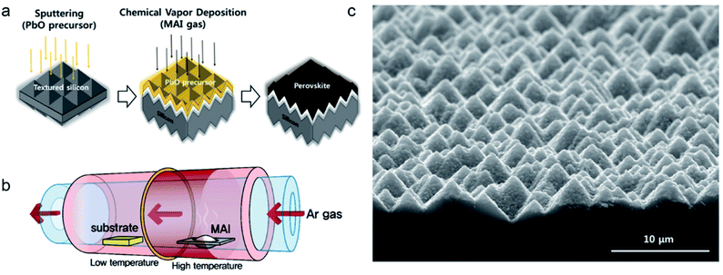 | ||
| Fig. 14 (a and b) Schematic drawing and (c) optical photo showing deposition of the perovskite film by hybrid CVD on a textured Si substrate. Reprinted from ref. 92 with permission from Elsevier. | ||
Considering the current density match in a perovskite/Si tandem solar cell, the perovskite layer with a large bandgap of around 1.7–1.8 eV is required.87,89 Due to the versatile tuning of compositions, CVD is also suitable for large bandgap perovskite deposition. CsPbI3 has been deposited on three different pyramidal size texture surfaces via CVD. It is shown that all the textured surfaces significantly reduce the reflectance by about 10%. Assuming a 100% internal quantum efficiency, this reduction of reflectance equals around 2 mA cm−2 short-circuit density.93 Further efforts are needed for CVD-deposited conformal pyramidal textured perovskite/Si tandem cells.
7. Modified CVD for flexible solar cells
CVD of perovskite is operated at a relatively low temperature below 160 °C, which is compatible with flexible substrates. Flexible perovskite thin films (CsPbBr3, and CsSnBr3) by CVD have been obtained.20,23 Although in these studies the perovskite films are used in photodetectors and resistive switching devices, they can also be used for the fabrication of flexible perovskite solar cells.On the other hand, due to a conformal coating feature, CVD is useful for deposition of a perovskite layer on non-flat surfaces, such as on the surface of a fiber. An interesting fiber-shaped perovskite solar cell has been fabricated by the versatile CVD technique, with a PCE up to 10.79% (Fig. 15).80 Similar to the planar-type solar cells, the coating of porous PbI2 around the fiber surface is needed for the effective diffusion of MAI vapor. The CVD helps the formation of high-quality perovskite layers on the curved fiber surface with a diameter of 250 μm, compared with the two-step solution-coating process. Currently the highest PCE is 10.79% for a fiber-shaped perovskite solar cell.80
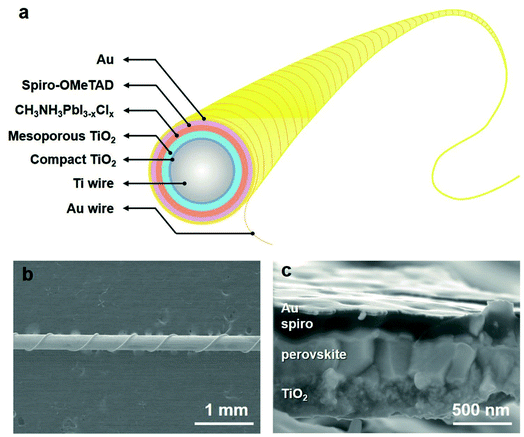 | ||
| Fig. 15 (a) Schematic drawing and (b) SEM image of fiber-shaped perovskite solar cells by CVD. (c) Cross-section SEM image of CVD deposited perovskite solar cell on a curved fiber surface. Reproduced from ref. 80 with permission from John Wiley and Sons. | ||
8. Cost analysis regarding modified CVD and solution processing
When considering the cost-performance analysis, there are several stages: (i) the fabrication cost for the perovskite solar module per m2, including the glass substrate, processing of perovskite solar module, frame, laminating film, junction-box and testing, which are so-called balanced of module (BOM); (ii) taken into account the PCE of the resulting module, one needs to calculate the fabrication cost per peak watt energy power output; (iii) assuming the lifetime of the module, combined with PCE degradation and average annual solar illumination, one needs to obtain the total energy output in the entire working life and the calculation of levelized cost of electricity (LCOE). To compare the LCOE, the manufacturing cost of a solar module, the PCE of the resulting module and the operational lifetime all contribute to the final results. To compare perovskite solar module manufacturing cost by solution process and CVD process, we assume the same module structure with ITO as the substrate. The other components such as glass substrate, lamination film and junction-box are also the same. The materials cost is also assumed to be the same with the same module area.There are several works on the cost-performance analysis of perovskite solar modules and tandem cells.94–99 For the analysis, several assumptions need to be clarified, e.g., the throughput/capacity of the factory (MW per year), factory operation time (hour per year), equipment footprint, factory location (in which country, the labor cost, footprint cost, installation cost, sales tax ext.), solar module efficiency (total area), solar module operational lifetime (degradation rate per year), and depreciation of equipment. Here in this review, we only focus on the manufacturing steps for perovskite layers. However, for the understanding of the difference, the idea for the cost-performance analysis and the above-mentioned assumptions should be noted. The cost for the equipment, maintenance, and the waste of raw materials will be taken into account.
Typically, the manufacturing cost for each square perovskite solar module is in the range of 37 to 140 dollars per m2.94–96 Based on these reports, the processing cost of perovskite module structure only contributes to 24% of the total module cost, which consists of glass substrates, processing of perovskite solar module, frame, laminating film, junction-box and testing (Fig. 16a). Furthermore, the coating of the perovskite layer contributes to only part of the processing of a perovskite solar module, and the cost for the fabrication of a p–i–n perovskite junction only contributes to 1.1% of the total cost (Fig. 16b).95 As calculated, the minimum sustainable prices (MSP) as a function of the assumed module efficiency is shown in Fig. 16c. One should note that this price is calculated without government subsidies, and this value is still lower than other mature photovoltaic techniques with subsides.
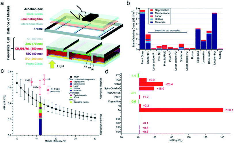 | ||
| Fig. 16 Cost-performance analysis of perovskite solar module in an inverted structure. (a) Schematic drawing showing a completed perovskite solar module with perovskite cells and other required components. (b) Manufacturing cost for each component of a completed perovskite solar module. (c) MSP of perovskite solar modules as a function of efficiency and comparing with other mature photovoltaic technologies. (d) The effect of changing perovskite materials and manufacturing process on the MSP (SSS: single-step solution process; SSV: single-step vapor deposition process; TSS: two-step solution process; TSH: two-step hybrid process). Reproduced from ref. 95 with permission from The Royal Society of Chemistry. | ||
What we are interested in is how much the cost will be affected by changing the solution coating process to a CVD process. As shown in Fig. 16d, the alternative of materials and processes for the manufacturing process has been provided. It can be seen that the changing of deposition process from one-step solution process to two-step hybrid deposition process, the MSP for selling only increased 0.5 cents per peak watt, which is 1.2% increase of the MSP.95 Similarly, in another cost-analysis performance work by Han and coworkers, they assumed a 100 MW capacity of perovskite solar modules by a factory manufacturing thin-film silicon solar cells (60 MW), which are deposited by plasma-enhanced CVD. By changing the deposition process from a plasma-enhanced CVD process to a solution process, the initial capital investment decreased from 26 million to 16 million dollars. However, when considering a rate of depreciation of 50%, the increase of cost based on the capital investment and manufacturing per peak watt is about 0.6 cents, on the 100 MW per year capacity.99 This indicated that the application of CVD does not lead to much difference on the manufacturing cost of perovskite solar modules.
Furthermore, the manufacturing cost for the two-terminal tandem solar module will only increase slightly due to the processing of a second subcell on the substrate. The manufacturing cost increased by $5.1 per m2.98 However, considering the output power increasing rate, the cost per peak watt is possible to be even lower. When considering the two-terminal tandem structure with a silicon subcell as substrate, and assuming an efficiency increase from 22.6% to 29.5% (the highest certified record for perovskite/silicon tandem cells), the output power under AM 1.5G increases from 226 W m−2 to 295 W m−2. The cost for high-efficiency crystalline heterojunction silicon solar cells is $79.31 per m2.100 The cost per peak watt further decreases by $0.062 per peak watt, which indicates that the tandem structure is one of the promising structures for further reducing the cost of photovoltaic. As discussed in Section 6, CVD is of great potential for high-efficiency perovskite/silicon tandem solar cells with the textured structure, which is beneficial for light management and absorption.
9. Conclusions and outlook
In this review article, we summarize the development of modified CVD for the fabrication of perovskite solar cells and modules. This technique is promising for large-scale fabrication. A high efficiency approaching 20% has been achieved on a small area.35 For future development, there are several potential directions. As summarized in Table 1, currently modified CVD based solar cells all use a regular n–i–p structure. An inverted structure has not been applied yet and might be a potential way to further improve the device performance and especially the operational stability. The second promising direction is application of the modified CVD methods for textured perovskite/silicon tandem solar cells, as introduced in Section 6. Further investigation on the rapid HCVD method to eliminate the extra ramping, cooling and stabilizing time may help improve the solar module efficiency as well as reducing cost. Modified CVD is promising for fabricating large-scale, low-cost perovskite solar cells with high stability. The cost for HCVD has a negligible effect on the levelized cost of energy compared with other solution coating processes, assuming the same module efficiency and lifetime. To further improve the stability and also efficiency, the defect passivation and interface modification are also important in modified CVD process. An attractive strategy is to combine the modified CVD and solution process together. For example, the defect passivation and interface modification for solution method can be applied in modified CVD deposited perovskite films. For example, solvent annealing post treatment,101 the grain boundary self-passivation by MAI,102 organic molecules,103 cation exchange,75 or other passivation additives such as FABr,104 PEAI,105 and recently bar-coated acetylcholine bromide,106 and so on. Furthermore, considering the main differences between solution-coated and modified CVD deposited perovskite layers, in-depth investigations are needed to reveal the underlying mechanisms responsible for shorter carrier lifetime and lower efficiency for modified CVD deposited perovskite solar cells.Conflicts of interest
There are no conflicts to declare.Acknowledgements
L. Q. acknowledges the funding by National Natural Science Foundation of China (NSFC) (22109067), and the research start-up grant by Southern University of Science and Technology. S. H. acknowledges the funding by NSFC (52103300), and start-up fund from Harbin Institute of Technology (Shenzhen) (HA45001121). Y. J. acknowledges the funding support from the Energy Materials and Optoelectronics Unit of Songshan Lake Materials Laboratory. Y. B. Q. acknowledges the support from the Energy Materials and Surface Sciences Unit of the Okinawa Institute of Science and Technology Graduate University.References
- M. A. Green, E. D. Dunlop, J. Hohl-Ebinger, M. Yoshita, N. Kopidakis and X. Hao, Prog. Photovoltaics, 2021, 29, 657–667 Search PubMed.
- T. Wu, Z. Qin, Y. Wang, Y. Wu, W. Chen, S. Zhang, M. Cai, S. Dai, J. Zhang, J. Liu, Z. Zhou, X. Liu, H. Segawa, H. Tan, Q. Tang, J. Fang, Y. Li, L. Ding, Z. Ning, Y. B. Qi, Y. Zhang and L. Han, Nano-Micro Lett., 2021, 13, 152 CrossRef CAS PubMed.
- L. Qiu, S. He, L. K. Ono, S. Liu and Y. B. Qi, ACS Energy Lett., 2019, 4, 2147–2167 CrossRef CAS.
- W. Tress, Adv. Energy Mater., 2017, 7, 1602358 CrossRef.
- N.-G. Park and K. Zhu, Nat. Rev. Mater., 2020, 5, 333–350 CrossRef CAS.
- Z. Li, T. R. Klein, D. H. Kim, M. Yang, J. J. Berry, M. F. A. M. van Hest and K. Zhu, Nat. Rev. Mater., 2018, 3, 18017 CrossRef CAS.
- Y. Vaynzof, Adv. Energy Mater., 2020, 10, 2003073 CrossRef CAS.
- M. R. Leyden, L. K. Ono, S. R. Raga, Y. Kato, S. Wang and Y. B. Qi, J. Mater. Chem. A, 2014, 2, 18742–18745 RSC.
- P. Luo, Z. Liu, W. Xia, C. Yuan, J. Cheng and Y. Lu, ACS Appl. Mater. Interfaces, 2015, 7, 2708–2714 CrossRef CAS PubMed.
- M. R. Leyden, Y. Jiang and Y. B. Qi, J. Mater. Chem. A, 2016, 4, 13125–13132 RSC.
- X. Liu, L. Cao, Z. Guo, Y. Li, W. Gao and L. Zhou, Materials, 2019, 12, 3304 CrossRef CAS PubMed.
- P. Luo, S. Zhou, W. Xia, J. Cheng, C. Xu and Y. Lu, Adv. Mater. Interfaces, 2017, 4, 1600970 CrossRef.
- D. J. Lewis and P. O'Brien, Chem. Commun., 2014, 50, 6319–6321 RSC.
- S. T. Ha, X. Liu, Q. Zhang, D. Giovanni, T. C. Sum and Q. Xiong, Adv. Opt. Mater., 2014, 2, 838–844 CrossRef CAS.
- G. Kim, S. An, S.-K. Hyeong, S.-K. Lee, M. Kim and N. Shin, Chem. Mater., 2019, 31, 8212–8221 CrossRef CAS.
- L. Qiu, S. He, Y. Jiang, D.-Y. Son, L. K. Ono, Z. Liu, T. Kim, T. Bouloumis, S. Kazaoui and Y. B. Qi, J. Mater. Chem. A, 2019, 7, 6920–6929 RSC.
- L. Qiu, S. He, Z. Liu, L. K. Ono, D.-Y. Son, Y. Liu, G. Tong and Y. B. Qi, J. Mater. Chem. A, 2020, 8, 23404–23412 RSC.
- M. R. Leyden, L. Meng, Y. Jiang, L. K. Ono, L. Qiu, E. J. Juarez-Perez, C. Qin, C. Adachi and Y. B. Qi, J. Phys. Chem. Lett., 2017, 8, 3193–3198 CrossRef CAS PubMed.
- G. Tong, X. Geng, Y. Yu, L. Yu, J. Xu, Y. Jiang, Y. Sheng, Y. Shi and K. Chen, RSC Adv., 2017, 7, 18224–18230 RSC.
- X. Li, X. Mo, Y. Xiang, G. Dai, P. He, M. Fang, J. Sun, H. Huang and J. Yang, J. Phys. D: Appl. Phys., 2020, 53, 354002 CrossRef CAS.
- S. V. N. Pammi, R. Maddaka, V.-D. Tran, J.-H. Eom, V. Pecunia, S. Majumder, M.-D. Kim and S. G. Yoon, Nano Energy, 2020, 74, 104872 CrossRef CAS.
- H.-D. Kim, S. V. N. Pammi, H.-W. Lee, S. W. Lee, S.-G. Yoon, J. Park, Y. J. Kim and H.-S. Kim, J. Alloys Compd., 2020, 815, 152404 CrossRef CAS.
- H. Wang, J. Lin, Y. Zhu, X. Zeng, H. Wei, P. Cheng, H. Lu, Y. Liu and R. Xiong, Adv. Electron. Mater., 2020, 6, 2000799 CrossRef CAS.
- P. Luo, Z. Liu, W. Xia, C. Yuan, J. Cheng and Y. Lu, J. Mater. Chem. A, 2015, 3, 12443–12451 RSC.
- M. M. Tavakoli, L. Gu, Y. Gao, C. Reckmeier, J. He, A. L. Rogach, Y. Yao and Z. Fan, Sci. Rep., 2015, 5, 14083 CrossRef PubMed.
- C.-R. Ke, D. J. Lewis, A. S. Walton, Q. Chen, B. F. Spencer, M. Z. Mokhtar, C. L. Compean-Gonzalez, P. O'Brien, A. G. Thomas and W. R. Flavell, ACS Appl. Energy Mater., 2019, 2, 6012–6022 CrossRef CAS.
- J. Yin, H. Qu, J. Cao, H. Tai, J. Li and N. Zheng, J. Mater. Chem. A, 2016, 4, 13203–13210 RSC.
- C. Mortan, T. Hellmann, M. Buchhorn, M. d'Eril Melzi, O. Clemens, T. Mayer and W. Jaegermann, Energy Sci. Eng., 2020, 8, 3165–3173 CrossRef CAS.
- Y. Jiang, M. Remeika, Z. Hu, E. J. Juarez-Perez, L. Qiu, Z. Liu, T. Kim, L. K. Ono, D. Y. Son, Z. Hawash, M. R. Leyden, Z. Wu, L. Meng, J. Hu and Y. B. Qi, Adv. Energy Mater., 2019, 9, 1803047 CrossRef.
- A. Ioakeimidis, C. Christodoulou, M. Lux-Steiner and K. Fostiropoulos, J. Solid State Chem., 2016, 244, 20–24 CrossRef CAS.
- A. Ng, Z. Ren, Q. Shen, S. H. Cheung, H. C. Gokkaya, S. K. So, A. B. Djurisic, Y. Wan, X. Wu and C. Surya, ACS Appl. Mater. Interfaces, 2016, 8, 32805–32814 CrossRef CAS PubMed.
- G. Kim, H. Min, K. S. Lee, D. Y. Lee, S. M. Yoon and S. I. Seok, Science, 2020, 370, 108–112 CrossRef CAS.
- J. J. Yoo, G. Seo, M. R. Chua, T. G. Park, Y. Lu, F. Rotermund, Y.-K. Kim, C. S. Moon, N. J. Jeon, J.-P. Correa-Baena, V. Bulović, S. S. Shin, M. G. Bawendi and J. Seo, Nature, 2021, 590, 587–593 CrossRef CAS.
- M. R. Leyden, M. V. Lee, S. R. Raga and Y. B. Qi, J. Mater. Chem. A, 2015, 3, 16097–16103 RSC.
- H. Lu, Y. Liu, P. Ahlawat, A. Mishra, W. R. Tress, F. T. Eickemeyer, Y. Yang, F. Fu, Z. Wang, C. E. Avalos, B. I. Carlsen, A. Agarwalla, X. Zhang, X. Li, Y. Zhan, S. M. Zakeeruddin, L. Emsley, U. Rothlisberger, L. Zheng, A. Hagfeldt and M. Grätzel, Science, 2020, 370, eabb8985 CrossRef CAS PubMed.
- L. Luo, Z. Ku, W. Li, X. Zheng, X. Li, F. Huang, Y. Peng, L. Ding and Y.-B. Cheng, Sci. Bull., 2021, 66, 962–964 CrossRef CAS.
- D. S. Bhachu, D. O. Scanlon, E. J. Saban, H. Bronstein, I. P. Parkin, C. J. Carmalt and R. G. Palgrave, J. Mater. Chem. A, 2015, 3, 9071–9073 RSC.
- Y. Peng, G. Jing and T. Cui, J. Mater. Chem. A, 2015, 3, 12436–12442 RSC.
- Q. Chen, H. Zhou, Z. Hong, S. Luo, H.-S. Duan, H.-H. Wang, Y. Liu, G. Li and Y. Yang, J. Am. Chem. Soc., 2014, 136, 622–625 CrossRef CAS PubMed.
- L. Luo, Y. Zhang, N. Chai, X. Deng, J. Zhong, F. Huang, Y. Peng, Z. Ku and Y.-B. Cheng, J. Mater. Chem. A, 2018, 6, 21143–21148 RSC.
- X. Zhu, D. Yang, R. Yang, B. Yang, Z. Yang, X. Ren, J. Zhang, J. Niu, J. Feng and S. F. Liu, Nanoscale, 2017, 9, 12316–12323 RSC.
- G. Tong, H. Li, G. Li, T. Zhang, C. Li, L. Yu, J. Xu, Y. Jiang, Y. Shi and K. Chen, Nano Energy, 2018, 48, 536–542 CrossRef CAS.
- P. Luo, S. Zhou, Y. Zhou, W. Xia, L. Sun, J. Cheng, C. Xu and Y. Lu, ACS Appl. Mater. Interfaces, 2017, 9, 42708–42716 CrossRef CAS PubMed.
- X. Deng, J. Hua, F. Huang, Y. Peng, W. Li, Z. Ku and Y.-b. Cheng, Sustainable Energy Fuels, 2020, 4, 2491–2496 RSC.
- X. Chen, Y. Myung, A. Thind, Z. Gao, B. Yin, M. Shen, S. B. Cho, P. Cheng, B. Sadtler, R. Mishra and P. Banerjee, J. Mater. Chem. A, 2017, 5, 24728–24739 RSC.
- X. Mo, X. Li, G. Dai, P. He, J. Sun, H. Huang and J. Yang, Nanoscale, 2019, 11, 21386–21393 RSC.
- S. Chen, J. Briscoe, Y. Shi, K. Chen, R. M. Wilson, S. Dunn and R. Binions, CrystEngComm, 2015, 17, 7486–7489 RSC.
- M. Afzaal and H. M. Yates, Surf. Coat. Technol., 2017, 321, 336–340 CrossRef CAS.
- M. Afzaal, B. Salhi, A. Al-Ahmed, H. M. Yates and A. S. Hakeem, J. Mater. Chem. C, 2017, 5, 8366–8370 RSC.
- H. Nishinaka and M. Yoshimoto, Jpn. J. Appl. Phys., 2016, 55, 100308 CrossRef.
- M. Aamir, M. Sher, M. D. Khan, M. A. Malik, J. Akhtar and N. Revaprasadu, Mater. Lett., 2017, 190, 244–247 CrossRef CAS.
- S. Basak, M. Afzaal and H. M. Yates, Mater. Chem. Phys., 2019, 223, 157–163 CrossRef CAS.
- J. C.-R. Ke, D. J. Lewis, A. S. Walton, B. F. Spencer, P. O'Brien, A. G. Thomas and W. R. Flavell, J. Mater. Chem. A, 2018, 6, 11205–11214 RSC.
- Y. Wu, A. Islam, X. Yang, C. Qin, J. Liu, K. Zhang, W. Peng and L. Han, Energy Environ. Sci., 2014, 7, 2934–2938 RSC.
- S. R. Raga, L. K. Ono and Y. B. Qi, J. Mater. Chem. A, 2016, 4, 2494–2500 RSC.
- Z. Liu, L. Qiu, E. J. Juarez-Perez, Z. Hawash, T. Kim, Y. Jiang, Z. Wu, S. R. Raga, L. K. Ono, S. F. Liu and Y. B. Qi, Nat. Commun., 2018, 9, 3880 CrossRef PubMed.
- F. Wang, H. Yu, H. Xu and N. Zhao, Adv. Funct. Mater., 2015, 25, 1120–1126 CrossRef CAS.
- Y. Wang, X. Guan, D. Li, H.-C. Cheng, X. Duan, Z. Lin and X. Duan, Nano Res., 2017, 10, 1223–1233 CrossRef CAS.
- T. Che, C. Shen, J. Gao, X. Ji, W. Kong and Y. Liu, Opt. Mater., 2020, 107, 110120 CrossRef CAS.
- T. Moser, K. Artuk, Y. Jiang, T. Feurer, E. Gilshtein, A. N. Tiwari and F. Fu, J. Mater. Chem. A, 2020, 8, 21973–21982 RSC.
- L. Qiu, Z. Liu, L. K. Ono, Y. Jiang, D. Y. Son, Z. Hawash, S. He and Y. B. Qi, Adv. Funct. Mater., 2019, 29, 1806779 CrossRef CAS.
- M. Batzill, K. Katsiev, J. M. Burst, U. Diebold, A. M. Chaka and B. Delley, Phys. Rev. B: Condens. Matter Mater. Phys., 2005, 72, 165414 CrossRef.
- M. Batzill, Sensors, 2006, 6, 1345–1366 CrossRef CAS.
- T. Bu, J. Li, H. Li, C. Tian, J. Su, G. Tong, L. K. Ono, C. Wang, Z. Lin, N. Chai, X. L. Zhang, J. Chang, J. Lu, J. Zhong, W. Huang, Y. B. Qi, Y. B. Cheng and F. Huang, Science, 2021, 372, 1327–1332 CrossRef CAS PubMed.
- C. Niu, C. Wang, G. Zhang, Q. Zhao, C. Fang, W. Li, F. Huang, Z. Ku and Y.-b. Cheng, Sol. RRL, 2021, 5, 2100102 CrossRef CAS.
- X. Wei, Y. Peng, G. Jing and T. Cui, Jpn. J. Appl. Phys., 2018, 57, 052301 CrossRef.
- M. H. Li, H. H. Yeh, Y. H. Chiang, U. S. Jeng, C. J. Su, H. W. Shiu, Y. J. Hsu, N. Kosugi, T. Ohigashi, Y. A. Chen, P. S. Shen, P. Chen and T. F. Guo, Adv. Mater., 2018, 30, e1801401 CrossRef PubMed.
- X. Li, D. Lin, Z. Chen, Z. Li, J. Wang, J. Chen, L. Gong, J. Xu, K. Chen, P. Liu and W. Xie, ACS Appl. Energy Mater., 2020, 3, 6544–6551 CrossRef CAS.
- C. P. Clark, B. Voigt, E. S. Aydil and R. J. Holmes, Sustainable Energy Fuels, 2019, 3, 2447–2455 RSC.
- A. F. Akbulatov, L. A. Frolova, S. A. Tsarev, I. Zhidkov, S. Y. Luchkin, E. Z. Kurmaev, K. J. Stevenson, S. M. Aldoshin and P. A. Troshin, J. Phys. Chem. C, 2020, 124, 21378–21385 CrossRef CAS.
- Y. Li, J. K. Cooper, R. Buonsanti, C. Giannini, Y. Liu, F. M. Toma and I. D. Sharp, J. Phys. Chem. Lett., 2015, 6, 493–499 CrossRef CAS PubMed.
- P.-S. Shen, J.-S. Chen, Y.-H. Chiang, M.-H. Li, T.-F. Guo and P. Chen, Adv. Mater. Interfaces, 2016, 3, 1500849 CrossRef.
- H. C. Gokkaya, S. Qian, Z. W. Ren, A. Ng and C. Surya, IEEE Photovoltaic Spec. Conf., 2017, 958–962 Search PubMed.
- W. G. Choi, D. W. Kang, S. Na, C. G. Park, F. P. Gokdemir and T. Moon, Nanoscale Res. Lett., 2018, 13, 9 CrossRef PubMed.
- Y. Jiang, M. R. Leyden, L. Qiu, S. Wang, L. K. Ono, Z. Wu, E. J. Juarez-Perez and Y. B. Qi, Adv. Funct. Mater., 2018, 28, 1703835 CrossRef.
- P. Luo, Y. Zhou, S. Zhou, Y. Lu, C. Xu, W. Xia and L. Sun, Chem. Eng. J., 2018, 343, 146–154 CrossRef CAS.
- Q. Shen, A. Ng, Z. Ren, H. C. Gokkaya, A. B. Djurisic, J. A. Zapien and C. Surya, ACS Appl. Mater. Interfaces, 2018, 10, 371–380 CrossRef CAS PubMed.
- V.-D. Tran, S. V. N. Pammi, V.-D. Dao, H.-S. Choi and S.-G. Yoon, J. Alloys Compd., 2018, 747, 703–711 CrossRef CAS.
- J. Chen, J. Xu, C. Zhao, B. Zhang, X. Liu, S. Dai and J. Yao, ACS Appl. Mater. Interfaces, 2019, 11, 4597–4606 CrossRef CAS.
- B. Dong, J. Hu, X. Xiao, S. Tang, X. Gao, Z. Peng and D. Zou, Adv. Mater. Technol., 2019, 4, 1900131 CrossRef CAS.
- S. Sanders, D. Stummler, P. Pfeiffer, N. Ackermann, G. Simkus, M. Heuken, P. K. Baumann, A. Vescan and H. Kalisch, Sci. Rep., 2019, 9, 9774 CrossRef CAS PubMed.
- C. Yang, X. Shan and T. Xie, Energies, 2019, 12, 4508 CrossRef CAS.
- S. Draguta, S. Thakur, Y. V. Morozov, Y. Wang, J. S. Manser, P. V. Kamat and M. Kuno, J. Phys. Chem. Lett., 2016, 7, 715–721 CrossRef CAS PubMed.
- S. V. N. Pammi, H.-W. Lee, J.-H. Eom and S.-G. Yoon, ACS Appl. Energy Mater., 2018, 1, 3301–3312 CrossRef CAS.
- M. Stolterfoht, C. M. Wolff, J. A. Márquez, S. Zhang, C. J. Hages, D. Rothhardt, S. Albrecht, P. L. Burn, P. Meredith, T. Unold and D. Neher, Nat. Energy, 2018, 3, 847–854 CrossRef CAS.
- Z. Yang, W. Zhang, S. Wu, H. Zhu, Z. Liu, Z. Liu, Z. Jiang, R. Chen, J. Zhou, Q. Lu, Z. Xiao, L. Shi, H. Chen, L. K. Ono, S. Zhang, Y. Zhang, Y. B. Qi, L. Han and W. Chen, Sci. Adv., 2021, 7, eabg3749 CrossRef CAS PubMed.
- T. Leijtens, K. A. Bush, R. Prasanna and M. D. McGehee, Nat. Energy, 2018, 3, 828–838 CrossRef CAS.
- A. Al-Ashouri, E. Kohnen, B. Li, A. Magomedov, H. Hempel, P. Caprioglio, J. A. Marquez, A. B. Morales Vilches, E. Kasparavicius, J. A. Smith, N. Phung, D. Menzel, M. Grischek, L. Kegelmann, D. Skroblin, C. Gollwitzer, T. Malinauskas, M. Jost, G. Matic, B. Rech, R. Schlatmann, M. Topic, L. Korte, A. Abate, B. Stannowski, D. Neher, M. Stolterfoht, T. Unold, V. Getautis and S. Albrecht, Science, 2020, 370, 1300–1309 CrossRef CAS PubMed.
- Y. Hou, E. Aydin, M. De Bastiani, C. Xiao, F. H. Isikgor, D. J. Xue, B. Chen, H. Chen, B. Bahrami, A. H. Chowdhury, A. Johnston, S. W. Baek, Z. Huang, M. Wei, Y. Dong, J. Troughton, R. Jalmood, A. J. Mirabelli, T. G. Allen, E. Van Kerschaver, M. I. Saidaminov, D. Baran, Q. Qiao, K. Zhu, S. De Wolf and E. H. Sargent, Science, 2020, 367, 1135–1140 CrossRef CAS PubMed.
- B. Chen, Z. J. Yu, S. Manzoor, S. Wang, W. Weigand, Z. Yu, G. Yang, Z. Ni, X. Dai, Z. C. Holman and J. Huang, Joule, 2020, 4, 850–864 CrossRef CAS.
- F. Sahli, J. Werner, B. A. Kamino, M. Brauninger, R. Monnard, B. Paviet-Salomon, L. Barraud, L. Ding, J. J. Diaz Leon, D. Sacchetto, G. Cattaneo, M. Despeisse, M. Boccard, S. Nicolay, Q. Jeangros, B. Niesen and C. Ballif, Nat. Mater., 2018, 17, 820–826 CrossRef CAS PubMed.
- J.-K. Hwang, S.-W. Lee, W. Lee, S. Bae, K. Cho, S. Kim, S. Lee, J. Y. Hyun, Y. Kang, H.-S. Lee and D. Kim, Thin Solid Films, 2020, 693, 137694 CrossRef CAS.
- K. Hamada, K. Yonezawa, K. Yamamoto, T. Taima, S. Hayase, N. Ooyagi, Y. Yamamoto and K. Ohdaira, Jpn. J. Appl. Phys., 2019, 58, Sbbf06 CrossRef CAS.
- N. L. Chang, A. W. Yi Ho-Baillie, P. A. Basore, T. L. Young, R. Evans and R. J. Egan, Prog. Photovoltaics, 2017, 25, 390–405 Search PubMed.
- Z. Song, C. L. McElvany, A. B. Phillips, I. Celik, P. W. Krantz, S. C. Watthage, G. K. Liyanage, D. Apul and M. J. Heben, Energy Environ. Sci., 2017, 10, 1297–1305 RSC.
- N. L. Chang, A. W. Y. Ho-Baillie, D. Vak, M. Gao, M. A. Green and R. J. Egan, Sol. Energy Mater. Sol. Cells, 2018, 174, 314–324 CrossRef CAS.
- Z. Li, Y. Zhao, X. Wang, Y. Sun, Z. Zhao, Y. Li, H. Zhou and Q. Chen, Joule, 2018, 2, 1559–1572 CrossRef CAS.
- Z. Song, A. B. Phillips, I. Celik, G. K. Liyanage, D. Zhao, D. Apul, Y. Yan and M. J. Heben, in 2018 IEEE 7th World Conference on Photovoltaic Energy Conversion (WCPEC) (A Joint Conference of 45th IEEE PVSC, 28th PVSEC & 34th EU PVSEC), 2018, pp. 1134–1138 Search PubMed.
- M. Cai, Y. Wu, H. Chen, X. Yang, Y. Qiang and L. Han, Adv. Sci., 2017, 4, 1600269 CrossRef.
- S. E. Sofia, H. Wang, A. Bruno, J. L. Cruz-Campa, T. Buonassisi and I. M. Peters, Sustainable Energy Fuels, 2020, 4, 852–862 RSC.
- Z. Xiao, Q. Dong, C. Bi, Y. Shao, Y. Yuan and J. Huang, Adv. Mater., 2014, 26, 6503–6509 CrossRef CAS.
- Z. Hawash, S. R. Raga, D.-Y. Son, L. K. Ono, N.-G. Park and Y. B. Qi, J. Phys. Chem. Lett., 2017, 8, 3947–3953 CrossRef CAS PubMed.
- D.-H. Kang, S.-Y. Kim, J.-W. Lee and N.-G. Park, J. Mater. Chem. A, 2021, 9, 3441–3450 RSC.
- S. Xiao, Y. Li, S. Zheng and S. Yang, MRS Bull., 2020, 45, 431–438 CrossRef.
- Q. Jiang, Y. Zhao, X. W. Zhang, X. L. Yang, Y. Chen, Z. M. Chu, Q. F. Ye, X. X. Li, Z. G. Yin and J. B. You, Nat. Photonics, 2019, 13, 460–466 CrossRef CAS.
- J. W. Yoo, J. Jang, U. Kim, Y. Lee, S.-G. Ji, E. Noh, S. Hong, M. Choi and S. I. Seok, Joule, 2021, 5, 2420–2436 CrossRef CAS.
| This journal is © The Royal Society of Chemistry 2021 |


