
 Open Access Article
 This Open Access Article is licensed under a
 Creative Commons Attribution 3.0 Unported Licence
Indirect bandgap, optoelectronic properties, and photoelectrochemical characteristics of high-purity Ta3N5 photoelectrodes†
Johanna
Eichhorn
 *a,
Simon P.
Lechner
a,
Chang-Ming
Jiang
a,
Giulia
Folchi Heunecke
a,
Frans
Munnik
b and
Ian D.
Sharp
*a
*a,
Simon P.
Lechner
a,
Chang-Ming
Jiang
a,
Giulia
Folchi Heunecke
a,
Frans
Munnik
b and
Ian D.
Sharp
*a
aWalter Schottky Institute and Physics Department, Technische Universität München, Am Coulombwall 4, 85748 Garching, Germany. E-mail: sharp@wsi.tum.de; johanna.eichhorn@wsi.tum.de
bHelmholtz-Zentrum Dresden-Rossendorf, Bautzner Landstraße 400, 01328 Dresden, Germany
First published on 26th August 2021
Abstract
The (opto)electronic properties of Ta3N5 photoelectrodes are often dominated by defects, such as oxygen impurities, nitrogen vacancies, and low-valent Ta cations, impeding fundamental studies of its electronic structure, chemical stability, and photocarrier transport. Here, we explore the role of ammonia annealing following direct reactive magnetron sputtering of tantalum nitride thin films, achieving near-ideal stoichiometry, with significantly reduced native defect and oxygen impurity concentrations. By analyzing structural, optical, and photoelectrochemical properties as a function of ammonia annealing temperature, we provide new insights into the basic semiconductor properties of Ta3N5, as well as the role of defects on its optoelectronic characteristics. Both the crystallinity and material quality improve up to 940 °C, due to elimination of oxygen impurities. Even higher annealing temperatures cause material decomposition and introduce additional disorder within the Ta3N5 lattice, leading to reduced photoelectrochemical performance. Overall, the high material quality enables us to unambiguously identify the nature of the Ta3N5 bandgap as indirect, thereby resolving a long-standing controversy regarding the most fundamental characteristic of this material as a semiconductor. The compact morphology, low defect content, and high optoelectronic quality of these films provide a basis for further optimization of photoanodes and may open up further application opportunities beyond photoelectrochemical energy conversion.
Introduction
Metal nitride semiconductors hold significant promise for photoelectrochemical (PEC) energy conversion,1,2 offering potential to overcome several limitations associated with the much more intensively investigated class of metal oxides.3,4 For example, substituting oxygen with nitrogen raises the energy of the valence band edge without affecting the energetic position of the conduction band edge.5 For photoanodes, this improves solar energy harvesting without significantly compromising the maximum obtainable photovoltage. In addition, the lower electronegativity of nitrogen compared to oxygen leads to mixed ionic-covalent bonds that may improve charge transport properties while retaining a high electronic tolerance to structural defects. In this context, tantalum nitride (Ta3N5) is an interesting photoanode material due to a bandgap of 2.1 eV, suitable band alignment for solar water splitting, and a theoretical photocurrent density limit of 12.5 mA cm−2 under AM 1.5G illumination, which corresponds to a maximum solar-to-hydrogen conversion efficiency of ∼15%.6–8Ta3N5 is commonly synthesized by nitridation of Ta2O5 films in ammonia atmosphere at high temperatures.9–12 The (opto)electronic quality of the Ta3N5 is strongly affected by the properties of the original oxide precursor, as well as the different ammonia (NH3) annealing conditions.10,13,14 A major drawback of the nitridation process is that oxygen must be substituted by nitrogen, causing volume contraction and, in turn, formation of disordered and porous films.12,15 Furthermore, the oxide-to-nitride conversion leaves high concentrations of residual oxygen within the Ta3N5 lattice, as well as other defects, such as nitrogen vacancies and reduced tantalum centers.10–12,16 Despite an apparent poor structural quality and large impurity content of such films, they achieve good PEC performance. Substitutional oxygen atoms on nitrogen sites (ON) have been suggested to form shallow donor states near the conduction band, which positively impacts PEC performance,12,17 though at much higher concentrations, oxygen increases the bandgap and decreases the charge carrier diffusion length.18,19 Nitrogen vacancies (VN) and reduced tantalum defects (Ta<5+), on the other hand, have been found to act as deep trap states that facilitate charge carrier recombination and play a major role in limiting the PEC performance.11,12,17 Overall, despite being a simple route for synthesizing high-performing Ta3N5 photoelectrodes, nitridation of Ta2O5 suffers from imprecise control of oxygen impurity and native defect concentrations. Moreover, the complex morphology and internal porosity of these films impede fundamental studies of electronic structure, chemical stability, and photocarrier transport, thus calling for alternative synthesis routes with enhanced defect control.
A possible strategy to improve material quality is direct synthesis from nitride precursors, which is technologically more challenging and, therefore, less explored. Previous studies have found that oxygen is critical for triggering formation of the Ta3N5 phase during sputtering and that the oxygen flow rate influences the PEC performance.18,20,21 Thus, even directly sputtered tantalum nitride contains high oxygen concentrations that impact electronic properties of the films. Here, we synthesize high quality Ta3N5 thin films with near ideal composition and low defect content by reactive magnetron sputtering and subsequent ammonia annealing at varying temperatures. We quantify the structural, optical, and photoelectrochemical properties as a function of the annealing temperatures by grazing incidence X-ray diffraction (GIXRD), Raman spectroscopy, photothermal deflection (PDS), photoluminescence (PL) spectroscopy, and linear sweep voltammetry. The high material quality enables us to provide new insights into the basic optoelectronic properties of Ta3N5 and the role of defects on its optoelectronic characteristics. As one of the main findings, we provide strong evidence that the nature of the Ta3N5 bandgap is indirect and that the commonly observed band-to-band photoluminescence is a consequence of disorder. The compact morphology, low defect concentration, and high optoelectronic quality of these films provide important insights into the semiconducting properties of this compound and may open up further application opportunities beyond photoelectrochemical energy conversion.
Experimental section
Synthesis of Ta3N5 thin films
Bixbyite Ta2N3 thin films were deposited on n+-type doped Si wafers (As, 〈100〉, Siegert Wafer GmbH) with native oxide and on fused silica glass (Siegert Wafer GmbH) by reactive magnetron sputtering (PVD 75, Kurt J. Lesker). Ta3N5 films on silicon substrates were used for PEC measurements and those on silica were used for optical characterization. Prior to deposition, silica substrates were cleaned consecutively in 1 vol% Hellmanex, acetone, and isopropanol using an ultrasonic bath. Subsequently, the substrates were dried with flowing nitrogen.For reactive sputter deposition, the Ta target (Kurt J. Lesker, 99.95%) was initially treated by sputtering with Ar plasma (Linde GmbH, 99.9999%) for 15 min at a pressure of 9.5 mTorr while applying 60 W DC sputtering power to the Ta target. Next, the target was conditioned by reactive sputtering using a process gas mixture of argon (2.9 mTorr), nitrogen (4.2 mTorr, Linde Electronics GmbH, 99.9999%), and oxygen (∼0.06 mTorr, Linde Electronics GmbH, 99.9999%) using a pulsed DC power supply operated at 100 kHz and a 98% duty cycle with a 50 W average power. Following conditioning, the thin film was sputtered on the substrate by opening the substrate shutter for 70 min. During the deposition, the substrate holder was rotated at 10 rpm, and was heated by an infrared lamp to 650 °C.
The sputtered amorphous tantalum nitride thin films were subsequently annealed in NH3 using a quartz tube furnace (Nabertherm RS 80/300/11) with an outer tube diameter of 25 mm. To investigate the influence of the annealing temperature on the material quality of the tantalum nitride thin films, a series of films were prepared between 820 °C and 980 °C. During the entire process, we used a constant NH3 flow of 100 sccm (Linde Electronics GmbH, 99.999%) at 1 bar. The samples were heated up with a ramp rate of 30 °C min−1 and were annealed at the temperature set point for 3 h. Afterwards, the furnace was switched off and allowed to cool down without interrupting the NH3 flow. At temperatures below 400 °C, we opened the heating unit around the tube to accelerate the cooling process. At room temperature, we switched to a continuous nitrogen purge flow for 10 min before removing the samples.
Material characterization
The crystalline phase and phase purity were analyzed by grazing incidence X-ray diffraction using a Rigaku SmartLab X-ray diffractometer with Cu Kα radiation at 0.5° grazing incidence angle. The 2θ diffraction angle was scanned between 15–70° with 0.04° steps.The film morphology was revealed by atomic force microscopy (AFM) using a Bruker Multimode under ambient conditions. For all measurements, PeakForce Mode and cantilevers with a nominal spring constant of 2.8 N m−1 were used. Scanning electron microscopy (SEM) cross section images were obtained with an NVision 40 FIB-SEM (Carl Zeiss) using the in-lens detector and an electron beam acceleration voltage of 5.0 kV.
X-ray photoelectron spectroscopy (XPS) was utilized to analyze the near-surface composition using a monochromatized Al Kα source (hν = 1486.6 eV) and a pass energy of 20 eV on a SPECS system. XPS binding energies were corrected by shifting the C 1s core level position to 284.8 eV. Spectral fitting was conducted using Casa XPS analysis software. For calculating the surface atomic composition of the annealed Ta3N5 films, we used the peak area of the corresponding N 1s, Ta 4f7/2 and O 1s peaks with the corresponding atomic sensitivity factors and effective attenuation length escape depth correction.
Elastic recoil detection analysis (ERDA) was conducted at the Ion Beam Centre of the Helmholtz-Zentrum Dresden-Rossendorf using a 43 MeV Cl7+ ion beam. The angle between the sample normal and the incoming beam was 75° and the scattering angle was 30°. The analyzed area was approximately 1.5 × 1.5 mm2. The recoil atoms and scattered ions were detected with a Bragg ionisation chamber. H recoils were detected with a separate solid state detector at a scattering angle of 40°. This detector was preceded by a 25 μm Kapton foil to stop scattered ions and heavy recoil ions. The depth resolution of this system is reduced because of energy loss straggling in the foil. The analysis was performed with the program Windf v9.3g.22
Optical characterization
Photothermal deflection spectroscopy was performed using a home-built system. PDS is based on the absorption of light, which results in local heating of the sample by non-radiative recombination of photoexcited carriers. Transfer of this heat to the surrounding medium leads to a change in the refractive index, which is probed by the deflection of a probe beam passing through the locally heated region of the surrounding medium. Here, the samples were immersed in perfluorohexane and illuminated at normal incidence by a chopped (9 Hz) monochromatized halogen light source. The probe beam was provided by a 635 nm laser diode (CPS635, Thorlabs) that propagated parallel to and near the sample surface. The beam deflection was monitored by a segmented detector, the output of which was read out using a lock-in amplifier.Photoluminescence spectroscopy was performed with a home-built system using an excitation wavelength of either 405 nm or 532 nm, as indicated in the text, in continuous wave operation. All measurements were performed in vacuum (p ≤ 10−5 mbar) at temperatures between 10 K and 300 K. The emitted light was collected with an Olympus LUCPlanFL (NA = 0.45) objective and analyzed with a monochromator (Horiba, iHR 550) equipped with a 300 lines per mm grating and a LN2-cooled charge-coupled-device (CCD) camera. Raman measurements were performed at room temperature in the same system with an excitation wavelength of 532 nm. The scattered light was analyzed with a 2400 lines per mm grating.
Variable angle spectroscopic ellipsometry was conducted using a J. A. Woollam M-2000X ellipsometer. Ψ and Δ were measured over a spectral range from 210 nm to 1688 nm at various reflection angles ranging from 45° to 70°. Analysis of the data was performed with the CompleteEASE software.
Photoelectrochemical measurements
The PEC performance was evaluated by linear sweep voltammetry using a Gamry potentiostat (reference 600) in a three-electrode setup with a Ag/AgCl reference electrode (3 M NaCl), the Ta3N5 photoanode as working electrode, and a Pt-wire as counter electrode. All measurements were performed with a scan rate of 100 mV s−1. Linear sweep voltammetry was conducted in 1 M KPi buffer at pH 12.3 in the presence of 0.1 M K4Fe(CN)6 as sacrificial hole acceptor in the dark and under front-side illumination using AM 1.5G simulated sunlight adjusted at 100 mW cm−2 (LOT-Quantum Design). Prior to the photoelectrochemical measurements, the electrolyte was bubbled with argon for 15 min.Results and discussion
Polycrystalline Ta3N5 thin films were synthesized on fused silica (SiO2) for optical characterization and on Si substrates for photoelectrochemical measurements. The synthesis reported here follows a two-step route but, in contrast to most prior reports, does not require the conversion of tantalum oxide to tantalum nitride. Rather, in the first step, tantalum nitride thin films were directly deposited by reactive magnetron sputtering, resulting in the formation of bixbyite-type Ta2N3. Subsequently, the films were converted into orthorhombic Ta3N5 by annealing in NH3 atmosphere with a flow rate of 100 sccm at varying temperatures (TNH3) for 3 h (Fig. 1).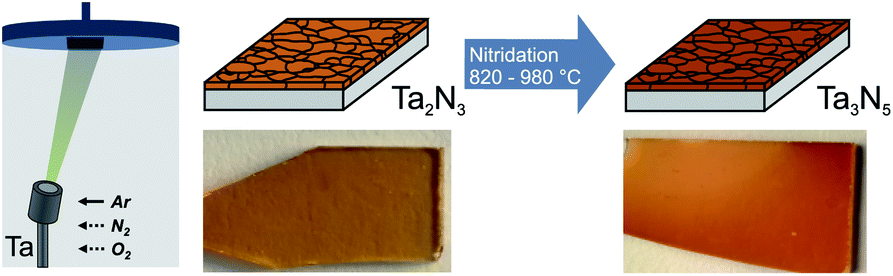 | ||
| Fig. 1 Schematic of the synthesis process for Ta3N5 thin films photoanodes. Amorphous Ta2N3 films were first deposited by reactive magnetron sputtering and were subsequently converted to polycrystalline Ta3N5 by annealing in NH3 for 3 h at varying temperatures. | ||
On both Si and SiO2 substrates, GIXRD patterns of as-grown films show weak peaks at approximately 31.3° and 36.4° (Fig. 2a and S1a†) indicative of bixbyite Ta2N3.23 On Si, reactive NH3 annealing at 820 °C leads to a mixed-phase GIXRD pattern with additional diffraction peaks corresponding to orthorhombic Ta3N5 (PDF# 79-1533).17,24,25 Temperatures >860 °C are necessary to fully convert the films into phase-pure Ta3N5. Compared to as-grown films, the peak at ∼31.4° is shifted towards higher angles after NH3 annealing up to 940 °C (close up in Fig. 2a), which reflects the phase transformation from bixbyite-type Ta2N3 to orthorhombic Ta3N5 films. The corresponding a, b, and c lattice constants of the orthorhombic lattice remain nearly constant for all temperatures, with values of 3.88 ± 0.01 Å, 10.17 ± 0.01 Å, and 10.25 ± 0.01 Å, respectively. The lattice parameters are slightly smaller compared to ideal Ta3N5, which has been previously assigned to the presence of defects within the material, in particular oxygen impurities and/or nitrogen vacancies.19,26,27 The peak area of all X-ray diffraction peaks increases up to 940 °C and starts to decrease for even higher temperatures, suggesting improved crystallinity up to this temperature and reduced crystallinity for higher temperatures. On fused silica (Fig. S1a†), we find a qualitatively similar behavior, however, slightly higher temperatures are required to convert the films compared to silicon.
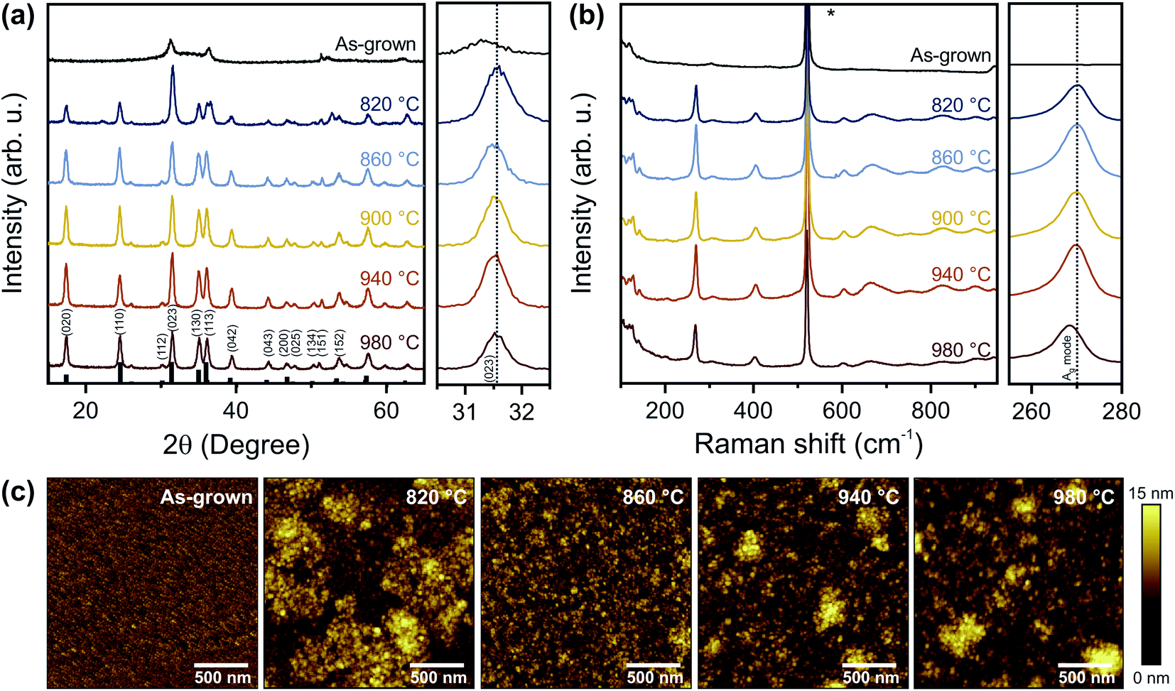 | ||
| Fig. 2 Structure and morphology of as-grown Ta2N3 and annealed Ta3N5 thin films on Si. (a) Grazing incidence X-ray diffraction patterns, (b) Raman scattering spectra, and (c) AFM images of as-grown Ta2N3 films and Ta3N5 films annealed at temperatures between 820 °C and 980 °C. In (a) the XRD reference spectrum of Ta3N5 is shown in black and the zoom-in image on the right side shows the Ta3N5 (023) diffraction peaks. In (b), the Raman mode related to the Si substrate is labelled with an asterisk and the zoom-in image on the right side shows the Ag Raman mode at 270 cm−1. The vertical dashed lines in (a) and (b) highlight the peak center at 900 °C to reveal relative peak shifts for annealing at lower and higher temperatures. | ||
To further confirm the phase composition of the synthesized Ta3N5 films, Raman spectroscopy was performed. Only after annealing, the films exhibit Raman modes (Fig. 2b) characteristic for Ta3N5.10,24 For the sample prepared at the highest temperature of 980 °C, the strength of the prominent Ag mode at 270 cm−1 is reduced and the peak position shows a distinct redshift (close up in Fig. 2b). A similar behavior is also observed after annealing at 980 °C on fused silica (Fig. S1b†). Additionally, the full width half maximum of the Raman peak is reduced for increasing annealing temperatures from 6.3 cm−1 at 860 °C to 5.6 cm−1 at 940 °C and increases to 6.2 cm−1 for even higher temperatures. These changes may be a direct consequence of additional disorder within the Ta3N5 lattice, in line with the reduced crystallinity observed by GIXRD. Overall, these findings indicate that as-grown Ta2N3 films can be successfully converted into Ta3N5 for annealing between 860 °C and 940 °C for 3 h. The results are consistent with the previously reported metastability of Ta2N3,23 as well as the instability of Ta3N5 at high temperatures in NH3 atmosphere.26 Although similar or higher temperatures are utilized for nitridation of Ta2O5, significantly longer annealing times of up to 120 h are required for achieving the conversion to Ta3N5.11,12,16,24,26 Thus, the direct nitride synthesis process reported here can significantly reduce processing times and ammonia consumption, which could have an important impact in enabling scalable fabrication of electronic grade Ta3N5 thin films.
The morphologies of the as-grown Ta2N3 film, as well as annealed Ta3N5 films were imaged by atomic force microscopy (Fig. 2c) and scanning electron microscopy (Fig. S2†). The as-grown film has a uniform morphology with a roughness of 1.1 nm and a grain size of ∼20 nm. After annealing at 820 °C, formation of islands is observed on the film surface. These morphological inhomogeneities are consistent with incomplete conversion to Ta3N5 (see also GIXRD above). Island formation also indicates volume expansion during the nitridation. Ellipsometry independently confirms an increase of film thickness by 11% from 53 nm for as-grown to 59 nm for completely converted films. These findings are in agreement with the phase transformation of bixbyite Ta2N3 into orthorhombic Ta3N5, which is characterized by a reduction in mass density from ∼11 g cm−3 to ∼9.8 g cm−3.23,28 The completely converted Ta3N5 films (TNH3 ≥ 860 °C) are homogenous and compact with slightly increased roughness of 2.3 nm and increased grain size of ∼30 nm (Fig. 2c and S1c†). It is important to note that in contrast to the approach presented here, conventional nitridation of tantalum oxide results in a volume contraction due to an increase in mass density, leading to the formation of cracks and pores within those films.12,15 Accordingly, direct nitride synthesis has the advantage of yielding dense films with reduced morphological voids compared to commonly applied oxide-to-nitride conversion strategies. For temperatures ≥940 °C, we observe the appearance of small islands on the surface (Fig. 2c and S1c†) and slightly increased porosity within the film (Fig. S2†), which could be an indication of material decomposition.
To understand the chemical changes arising from NH3 annealing, the bulk and surface composition were determined by elastic recoil detection analysis and X-ray photoelectron spectroscopy directly after sputter deposition, as well as after subsequent NH3 annealing (Table 1). The as-grown Ta2N3 films exhibit a high oxygen (18.0 at%) and low nitrogen (46.1 at%) content. With increasing temperature up to 940 °C, the nitrogen content increases to 62 at% and the oxygen content decreases to 2.4 at%, corresponding to N/Ta and O/Ta ratios of 1.77 and 0.07, respectively. A similar bulk composition was previously reported for sputtered Ta3N5 films.27 These chemical changes in the bulk agree with the changes in surface composition determined by XPS, which reveal an increase of the N/Ta ratio to ∼1.7 and a systematic decrease of the O/Ta ratio to ∼0.2 with increasing annealing temperature (Table 1). Compared to ERDA, the measured O/Ta ratios by XPS are significantly higher due to the formation of a thin surface oxide layer from air exposure. For the highest temperatures, the O/Ta ratio remains constant in the bulk, while the N/Ta ratio decreases slightly. The latter loss of nitrogen is even more pronounced at the surface, which is reflected by a decrease of the N/Ta ratio to 1.6. Overall, these changes in composition agree with GIXRD and Raman measurements, indicating material decomposition starting from the surface at the highest annealing temperature. Additionally, ERDA indicates that the hydrogen content within all the annealed films is extremely low, with a value of ∼0.5%.
| Sample | ERDA | XPS | ||||||
|---|---|---|---|---|---|---|---|---|
| Ta (at%) | N (at%) | O (at%) | H (at%) | N/Ta | O/Ta | N/Ta | O/Ta | |
| As-grown | 34.6 | 46.1 | 18.0 | 1.2 | 1.33 | 0.52 | 0.93 | 1.15 |
| 860 °C | 34.1 | 62.1 | 3.2 | 0.6 | 1.82 | 0.09 | 1.78 | 0.22 |
| 940 °C | 35.1 | 62.0 | 2.4 | 0.5 | 1.77 | 0.07 | 1.59 | 0.23 |
| 980 °C | 35.5 | 61.4 | 2.7 | 0.4 | 1.73 | 0.08 | 1.64 | 0.22 |
Typical N/Ta and O/Ta ratios reported for the synthesis of Ta3N5 thin films via the nitridation of Ta2O5 are in the range of 1.1–1.5 and 0.25–1.3 12,15,16,29, while those obtained from reactive magnetron sputtering and subsequent ammonia annealing are in the range of 0.5–1.8 and 0.1–0.6, respectively.20,21,30 The N/Ta ratios reported here are significantly higher than most prior literature reports and are very close to the ideal stoichiometric value. Furthermore, our films are characterized by very low O/Ta ratios, with nearly an order of magnitude improvement over most reported nitrided Ta2O5 films. In this context, Henderson et al. demonstrated that oxygen residuals in Ta3N5 cannot be fully removed and an O/Ta ratio of 0.07 was reported even after 120 h of NH3 annealing. The underlying reason is likely that the partial replacement of nitrogen by oxygen in the Ta3N5 lattice plays a crucial role in stabilizing the +5 oxidation state of Ta.26 However, substitutional ON is known to be a shallow donor and residual amounts of these defects are likely beneficial for achieving desired n-type conductivity of photoanodes.31–33
The films were further characterized by XPS to study the bonding structure and the chemical composition at the surface. Fig. 3a shows high-resolution Ta 4f and O 1s core level spectra, reflecting the main chemical and compositional changes of the surfaces. The Ta 4f spectrum can be deconvoluted into four doublets, which arise from reduced tantalum species (Ta 4f7/2 23.2 eV, bright blue), tantalum nitride (Ta 4f7/2 24.8 eV, grey), tantalum oxynitride (Ta 4f7/2 25.7 eV, medium blue), and tantalum oxide (Ta 4f7/2 26.6 eV, dark blue).5,8,12,34–38 The main Ta 4f7/2 peak (grey) is shifted from 24.4 eV for as-grown films to 24.8 eV after NH3 annealing, which is consistent with the change of average oxidation state from +4.5 for bixbyite Ta2N3 (ref. 23) to +5 for orthorhombic Ta3N5.5,37 The three peaks in the O 1s region (Fig. 3a) can be assigned to Ta–O bonds (∼530 eV, red), corresponding to oxygen in the Ta3N5 lattice, as well as hydroxyl groups (∼532 eV, orange) and adsorbed water (∼533 eV, yellow) on the surface.8,12,17 For the N 1s spectrum (Fig. S3†), we find two components corresponding to Ta–N bonds (396.5 eV) and N–Ta–O bonds (398.0 eV).
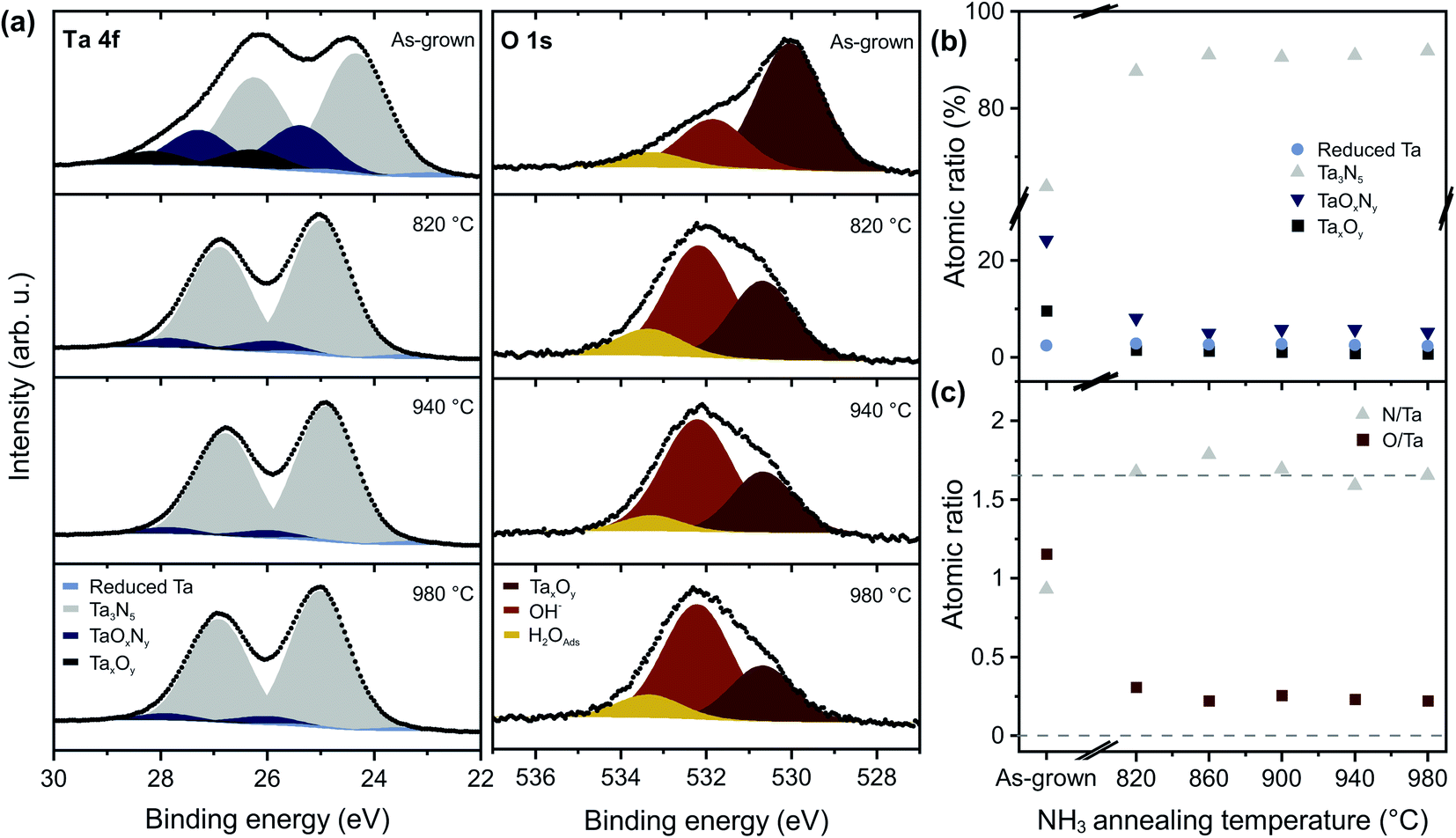 | ||
| Fig. 3 Surface composition of Ta3N5 thin films on silicon. XPS core-level spectra of Ta 4f and O 1s (a) of as-grown tantalum nitride thin films compared to those measured after annealing in NH3 atmosphere. Atomic ratios of the tantalum composition (b) as well as N/Ta and O/Ta ratios (c) within the tantalum nitride thin films obtained by XPS as a function of the NH3 annealing temperature. | ||
Annealing at 820 °C converts the film to Ta3N5, while also significantly decreasing the oxygen content, as well as the contribution from TaOxNy and TaxOy. For TNH3 > 860 °C, the contribution of the Ta3N5 component to the film composition reaches a maximum of 91% (Fig. 3b and S4a†). For Ta3N5 photoanodes, the concentration of chemically reduced Ta is of particular importance, since such centers act as deep level defects that have been implicated in carrier trapping and poor PEC performance.10,12,15,39 Our Ta3N5 films are characterized by a reduced Ta content of only 2.5 at%, which is significantly lower than the concentrations of up to 25 at% that have been reported after nitridation of Ta2O5.12,40 The reducing nature of the NH3 gas environment is known to prevent oxidation of Ta3+ to Ta5+, meaning that the defect content in annealed films is highly sensitive to the starting film composition. For the nitridation of Ta2O5, a decrease of the Ta3+ content from 25 at% to 10 at% was observed with increasing NH3 flow rates, which was phenomenologically assigned to the elimination of nitrogen vacancies within the material.12 However, the remaining Ta3+ content arising from the sub-stoichiometric oxygen content of the oxide precursor could not be further eliminated via the reactive annealing procedure. By contrast, in our work, we find that the concentration of reduced Ta is small and largely independent of the NH3 annealing temperature (Fig. 3b and S4a†), to within the sensitivity of our instrument. This is a natural consequence of the improved stoichiometry of the films, enabled by the direct nitride synthetic route, and results in the formation of high quality Ta3N5 films with high N/Ta and low O/Ta ratios (Fig. 3c and S4b†) as well as significantly lower electronically active deep level defect concentrations.
Having characterized the structural and compositional properties, we now turn to the optical properties of the films. The improved stoichiometry, density, and planarity of the films reported here enable more robust optical analysis than the porous and defective films typically generated by nitridation of oxides. This is important since many basic semiconductor properties of Ta3N5 remain unknown or controversial. Prominent among these is the nature of the fundamental bandgap, which has been inconsistently assigned as both direct and indirect within the literature.19,24,31,41–44
To address the fundamental question of the nature of the optical bandgap of Ta3N5, the optical absorption spectra of the different Ta3N5 films on silica were measured by photothermal deflection spectroscopy (Fig. 4a). Compared to conventional absorption spectroscopy, PDS has the advantage of extremely high sensitivity and dynamic range, which allows the quantitative detection of weak defect-related sub-bandgap features and Urbach tails (see below). Furthermore, PDS is insensitive to unwanted scattering processes and allows accurate determination of the absorption edge features. For TNH3 ≥ 860 °C, a strong optical absorption onset at ∼600 nm is present, corresponding to band-to-band excitation. The Tauc plot for an indirect transition (Fig. 4b) reveals two linear regimes for the representative sample treated at TNH3 = 940 °C. This behavior is characteristic of an indirect semiconductor, where the band-to-band transition requires both photon absorption and absorption or emission of a phonon with energy ℏω corresponding to Eg − ℏω and Eg + ℏω, respectively. Thus, analysis of our samples indicates that Ta3N5 is an indirect semiconductor, with a bandgap of 2.18 eV. Adding further support to this conclusion, the phonon energy extracted from the Tauc plot is ℏω = 0.11 eV, which agrees with both theoretical calculations for the optical phonon energy of 0.108 eV (ref. 42) and the experimentally observed vibrational mode at 910 cm−1 (Fig. 2b). In addition to the indirect bandgap at 2.18 eV, we also find evidence for a direct transition near 2.56 eV (Fig. S5†). The energy of this transition is consistent with known optical anisotropy of Ta3N5, which results in a bandgap of ∼2.1 eV along the a-axis and ∼2.5 eV along the b- and c-axes of the orthorhombic lattice.24,26,42
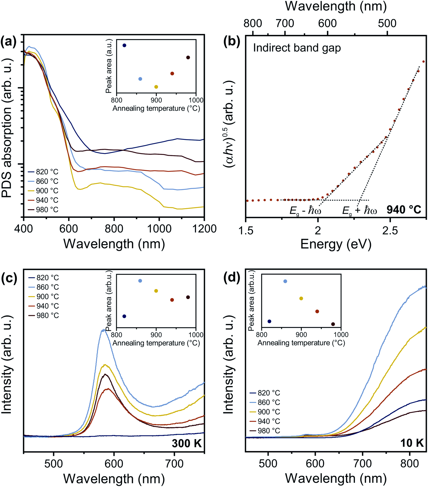 | ||
| Fig. 4 Effect of annealing temperature on the optical properties of Ta3N5 thin films on fused silica. (a) PDS spectra of Ta3N5 thin films for increasing annealing temperatures. (b) Indirect bandgap Tauc plots for Ta3N5 annealed at 940 °C. (c) Room temperature PL emission spectra for increasing annealing temperatures from 820 °C to 980 °C using 405 nm excitation. (d) Low temperature PL emission spectra for increasing annealing temperatures from 820 °C to 980 °C measured at 10 K and 405 nm excitation. The insets in a, c, and d show the integrated area of the sub-gap absorption, and PL peaks, respectively. | ||
We note that Ta3N5 films prepared by nitridation of Ta2O5 often show only one linear regime for the indirect bandgap Tauc analysis,12,16,45 which is likely a consequence of strong optical scattering from porous layers, as well as significant structural disorder associated with high defect densities. Not only can these non-idealities introduce uncertainty into the absolute magnitude of the bandgap, but they can also complicate analysis of whether the transition is direct or indirect.46 Here, the low optical scattering from dense, planar films, as well as the near-ideal stoichiometric composition, reduce such contributions, simplifying analysis of the basic optical material properties. Indeed, the structural and compositional quality of our films is reflected in a small Urbach energy <50 meV (Table S1†) determined by fitting spectroscopic ellipsometry data with a general oscillator model (Fig. S6†), which compares favorably with 160 meV obtained from nitridation of Ta2O5.12 Bandgaps determined by optical absorption have previously yielded values in the range of 2.06 eV to 2.1 eV, while band edge photoluminescence has been detected at 2.13 eV (see description below for the origin of PL across the indirect bandgap). In the present work, the bandgap of 2.18 eV measured by PDS on high quality films resolves this prior inconsistency between bandgap energy and apparently blue shifted PL emission energy.
Next, we discuss the defect-related sub-gap optical absorption obtained from PDS to gain further insights into the formation and/or elimination of defects during NH3 annealing. Before complete conversion to Ta3N5 (TNH3 = 820 °C, dark blue curve), the sub-gap optical absorption (wavelength > 750 nm) increases with increasing wavelength, consistent with free carrier absorption in metallic Ta2N3 (Fig. 4a).23 For the converted films, the sub-gap absorption is reduced up to TNH3 = 900 °C (inset of Fig. 4a) and is characterized by a distinct absorption band between 650 nm and 1000 nm, which is most pronounced for TNH3 = 860 °C (light blue curve) and TNH3 = 900 °C (yellow curve). A similar absorption feature is often reported for Ta3N5.11,14,16,31,33,47 The underlying origin is still under discussion and recent studies assigned the sub-bandgap absorption feature to the presence of defects such as reduced Ta,30,39,47 VN,11,33 or ON.31 The corresponding absorption processes were attributed to trapping and de-trapping of (nearly-)free conduction band electrons at Ta4+/Ta5+ centers, to the electron transition from  to
to  , and to the excitation from formed deep metallic states to empty Ta 5d states above the conduction band edge, respectively. In the present study, the sub-gap optical absorption feature decreases in strength from TNH3 = 860 °C to 940 °C, which correlates with a decrease of the oxygen content, as observed by XPS (Fig. S7†). We note that our films show a slight over-stoichiometry of N/Ta and thus the formation of nitrogen vacancies is rather unlikely at low temperatures, which is in contrast to previous studies on nitridated Ta2O5 with sub-stoichiometric N/Ta ratios.25,26 Therefore, we correlate the reduction of sub-gap optical absorption with the elimination of ON for increasing NH3 annealing temperature.
Notably, the sub-bandgap absorption rises again for the highest annealing temperatures (inset of Fig. 4a). Yet, the spectral signature is subtly different; rather than exhibiting the characteristic band in the range of 650–1000 nm, it is spectrally flat, extending out to the longest wavelengths measured (orange and red curve in Fig. 4a). This variation of the absorption correlates with the reduced N/Ta ratio revealed by XPS and ERDA (see also Fig. S7†). Taken together, these results indicate formation of nitrogen vacancies at high annealing temperatures leading to increased sub-bandgap absorption with a flat spectral profile. This is in line with previous studies, in which the loss of nitrogen was reported after prolonged NH3 annealing, as well as at high temperatures (TNH3 ≥ 900 °C), due to material decomposition.11,26,41
Our absorption spectra further agree with a recent study by Nurlaela et al., who investigated the absorption properties of partially oxidized Ta3N4.83O0.17 and nitrogen deficient Ta3N4.83.31 While the absorption of Ta3N4.83O0.17 exhibits the characteristic sub-bandgap absorption feature, the sub-gap optical absorption of Ta3N4.83 shows a rather flat spectral response extending towards longer wavelengths.12,31 Such sub-gap absorption was previously also reported for Ta3N5 synthesized by nitridation of Ta2O5, which possessed a low N/Ta ratio (i.e. large VN concentration) and high content of reduced tantalum.12,17 In summary, we assign the initial reduction in sub-gap optical absorption with increasing annealing temperature to a decrease of the oxygen impurity concentration. Higher temperatures favor nitrogen loss, while the oxygen content remains mainly constant, which likely leads to increased nitrogen vacancy concentrations and the appearance of increased sub-gap absorption.
In addition to modifying optical absorption, the defect content in Ta3N5 films has a strong influence on optical emission properties. Given the indirect bandgap of the material, it is expected that band edge photoluminescence should be weak or even undetectable from this semiconductor. Nevertheless, various studies have reported band edge PL near 2.13 eV.12,16 To understand the origin of this emission from indirect bandgap Ta3N5, as well as defect-related sub-bandgap features, we first performed steady state PL spectroscopy at room temperature (Fig. 4c). Ta2N3 films prepared at 820 °C have negligible PL (dark blue curve). For all other films, the PL spectra consist of a main emission peak, with a maximum amplitude at approximately 585 nm (2.12 eV), asymmetrically broadened to longer wavelengths. The low-energy PL tail could be induced by disorder within the material and can be used to extract the Urbach energy using the van Roosbroeck–Shockley equation.48 The Urbach energy is rather small, with a value of ∼45 meV, in good agreement with the Urbach energy independently determined by our ellipsometry and confirming the good structural quality of the films.
For increasing annealing temperatures up to 940 °C, the band edge luminescence decreases and then increases again for TNH3 = 980 °C (Fig. 4c). Based on our structural characterization, this finding implies that the PL intensity decreases with improved material quality. If the material possessed a direct bandgap, reduced disorder should improve the radiative efficiency of band-to-band recombination. The exact opposite behavior is observed here. This provides further evidence for the indirect bandgap, whereby disorder-induced relaxation of the momentum selection rule increases the band-to-band recombination rate relative to defect-mediated recombination. As the film quality is increased, participation of phonons during band-to-band recombination is more strictly required. Therefore, the band-to-band recombination rate decreases and recombination over defects becomes dominant. This interpretation is consistent with the change of PL intensity with annealing, as well as the analysis of optical absorption spectra presented above.
Low temperature photoluminescence measurements provide additional insight into defect-related optical transitions. To probe different depths within the material, we used 532 nm and 405 nm for bulk and surface sensitive PL excitation, respectively, corresponding to a penetration depth of 210 nm and 25 nm for Ta3N5 prepared at 940 °C. For both excitation wavelengths, the PL spectra collected at 10 K (Fig. 4d and S8†) show a broad sub-bandgap emission between 600 nm and 900 nm, which is qualitatively similar to previous studies.12,16 In particular, recent analysis of PL spectra from Ta3N5 films produced via nitridation of Ta2O5 allowed the identification of two distinct emission peaks, one centered at 730 nm arising from nitrogen vacancies and the other centered at 830 nm assigned to reduced Ta species.12 In that work, the films showed high concentrations of both defect types. The major impact of NH3 treatment was determined to be the elimination of VN, which resulted in decreasing intensity of sub-gap PL. However, the 730 nm and 830 nm signals were not affected proportionally, since reduced Ta centers unassociated with VN states remained in the films. This finding highlighted the importance of the film quality prior to nitridation due to the inability of NH3 annealing to directly convert Ta3+ into Ta5+.
In the present work, we find no indication for the distinct sub-gap PL feature at 730 nm that was previously attributed to VN. This is consistent with our films having near-ideal N/Ta stoichiometry, resulting in small VN concentrations. Rather, we observed a single broad emission band from the surface and bulk of the material that, upon complete conversion to Ta3N5 (TNH3 ≥ 860 °C), monotonically decreases with increasing annealing temperature (inset in Fig. 4d and S8b†). Analysis of PL data reveals thermally activated quenching of the sub-gap emission, with similar activation energies of 28 ± 4 meV for all annealing temperatures and wavelengths (Fig. S9 and S10†), indicating a shared mechanism and defect type. This observation is initially surprising, given that NH3 annealing at 980 °C was shown to introduce nitrogen vacancies, resulting in increased sub-bandgap optical absorption, shifted Raman modes, decreased N/Ta ratios, and increased band-to-band emission. Therefore, it is unlikely that the sub-gap emission observed here originates from reduced tantalum species due to nitrogen vacancies. Rather, the decreased intensity of this emission peak is strongly correlated with the reduction of TaxOy content (Fig. S7†), which agrees with the previous assignment of Fu et al.16 While Fu et al. assigned the PL to recombination over oxygen defects at the surface, we determine reduced defect densities both in the bulk and at the surface by using PL with different excitation wavelength (Fig. S8†).
For light absorbers, the nature of the bandgap is especially important since indirect semiconductors are generally characterized by weaker band-edge optical absorption coefficients, which introduces additional challenges for ensuring that the optical absorption depth is physically matched with the charge extraction length. Furthermore, the lack of efficient radiative band-to-band recombination in indirect semiconductors precludes their use in light emission applications and prevents energy conversion efficiency gains that can be realized by internal photon recycling. The finding that Ta3N5 is an indirect bandgap semiconductor highlights the importance of understanding and controlling defect-mediated recombination processes in order to improve the charge extraction efficiency. In contrast to a direct bandgap semiconductor, in which improved PL efficiency correlates with improved optoelectronic quality, for indirect bandgap Ta3N5 not just the sub bandgap but also the disorder-induced band edge emission should be minimized.
Lastly, to understand the impact of defect properties on energy conversion efficiencies, we characterized the PEC performance of Ta3N5 films on degenerately n+-doped silicon substrates. In prior reports, the synthesis of Ta3N5 by nitridation of Ta2O5 is often optimized for PEC applications with a strong focus on high current densities and low onset potentials. The investigated photoelectrodes usually have a thickness in the range of several hundred nanometers and exhibit a relatively high porosity and roughness arising from the volume contraction during oxide-to-nitride conversion. In contrast, our sputtered Ta3N5 films are thin (60 nm) and have a compact, homogenous structure resulting in minimized surface area. Thus, our films are not optimized for PEC performance, but are instead tailored for systematic analysis of correlations of chemical composition and fundamental (opto)electronic properties with their PEC properties.
PEC measurements were conducted in 1 M phosphate buffer (KPi, pH 12.3) with 0.1 M K4Fe(CN)6 as hole scavenger under AM 1.5G illumination (Fig. 5). The onset potential improves from 1.1 V to 0.6 V with increasing annealing temperature. Additionally, the photocurrent density at 1.23 V vs. reversible hydrogen electrode (RHE) increases from 0.3 mA cm−2 to 0.8 mA cm−2 for increased temperatures from 860 °C to 940 °C. Interestingly, the photocurrent density decreases again to 0.5 mA cm−2 at TNH3 = 980 °C. The photocurrent densities are higher compared to previous studies on sputtered Ta3N5 photoelectrodes,18,20,21 and similar to sputtered Ta3N5 films after subsequent NH3 treatment.20
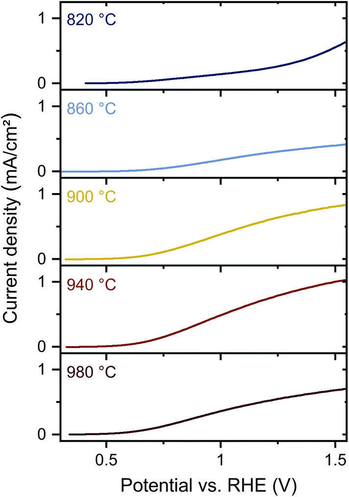 | ||
| Fig. 5 Photoelectrochemical performance of Ta3N5 thin films annealed in NH3 at different temperatures. Current–potential curves for Ta3N5 films on silicon substrates annealed at temperatures between 820 °C and 980 °C. The photoelectrochemical performance was recorded in 1 M phosphate buffer (pH 12.3) in the presence of 0.1 M K4Fe(CN)6 as hole scavenger and under front side illumination (AM 1.5G, 100 mW cm−2). | ||
In our study, the improved PEC performance at moderate temperatures correlates again with the improved material quality indicated by reduced defect PL emission, lower sub-bandgap absorption, and decreased tantalum oxide content. After annealing at 980 °C, the PEC performance decreases, indicating material degradation, which is consistent with observed Raman shifts, reduced N/Ta ratios, and diminished (opto)electronic properties. Overall, the improved PEC performance can be associated with the elimination of oxygen impurities, whereas the decreased PEC performance at the highest annealing temperature is consistent with defect formation due to material decomposition. A transition between both regimes is represented by TNH3 = 940 °C. Although PDS indicates that formation of nitrogen vacancies occurs at this annealing temperature, PL measurements show overall improved material quality and the removal of oxygen impurities, which yields improved PEC characteristics. In contrast, for the highest temperature significant reduction of material quality is found by all characterization methods, which causes a decrease in the photoelectrochemical performance.
Next, we compared the PEC characteristics with and without sacrificial hole acceptor (Fig. S11a†) and calculated the charge separation efficiency, Φsep, and charge injection efficiency, Φinj, according to the method in ref. 49. The charge separation efficiency represents the fraction of photogenerated carriers that reach the semiconductor–electrolyte interface. Here, we find that Φsep increases up to 940 °C and then decreases again (Fig. S11b†). Thus, the charge separation efficiency correlates with the changes in material quality. By contrast, the charge injection efficiency, which represents the charge transfer yield across the semiconductor/electrolyte interface for water oxidation, does not appear to be directly correlated with the annealing condition or material quality (Fig. S11c†). In particular, for all temperatures ≥900 °C, low injection efficiencies are observed at 1.23 V vs. RHE. Both Φsep and Φinj are similar to previously reported values for Ta3N5 photoelectrodes.50–52 Accordingly, improved material quality and reduced disorder increase the charge separation efficiency, but only slightly affect the charge injection efficiency, confirming the importance of integrating a catalyst onto the surface for driving water oxidation.
Summary
Using a two-step route, we synthesized homogenous and compact Ta3N5 thin films with near-ideal stoichiometric composition and low defect densities. Ta2N3 films were synthesized by reactive magnetron sputtering and subsequently converted to Ta3N5 by annealing in NH3 at varying temperatures. Both the crystallinity and material quality improve for increasing annealing temperatures up to 940 °C, while higher temperatures introduce additional disorder within the Ta3N5 lattice, leading to reduced photoelectrochemical performance. These changes are also reflected in the surface and bulk composition, showing the elimination of oxygen impurities at moderate and the loss of nitrogen at high temperatures. As a consequence, defect-related sub-gap optical absorption initially decreases due to reduced oxygen impurity concentration, and subsequently increases due to increased formation of nitrogen vacancies. The high structural and compositional quality of these films at optimized annealing conditions is also reflected in the small Urbach energy and enables us to unambiguously identify the nature of the Ta3N5 bandgap as indirect. The suppression of the band-edge photoluminescence with improved material quality correlates with decreased disorder within the Ta3N5 films, providing further evidence for the assignment of Ta3N5 as an indirect bandgap semiconductor. Overall, this resolves a long-standing controversy regarding the most fundamental characteristic of Ta3N5 as a semiconductor. The high quality of the fabricated films, as well as elucidated defect characteristics, provide important information for optimization of properties of relevance not only for photoelectrochemical energy conversion, but also for other future applications of Ta3N5 material as an electronic grade semiconductor.Conflicts of interest
There are no conflicts to declare.Acknowledgements
This project has received funding from the European Research Council (ERC) under the European Union's Horizon 2020 research and innovation programme (grant agreement no. 864234). J. E. acknowledges funding by the Deutsche Forschungsgemeinschaft (DFG, German Research Foundation) – Grant No. 428591260 and support from the Bavarian Academy of Sciences and Humanities. We further acknowledge support from Deutsche Forschungsgemeinschaft (DFG, German Research Foundation) under Germany's Excellence Strategy – EXC 2089/1 – 390776260 and TUM. Solar in the context of the Bavarian Collaborative Research Project Solar Technologies Go Hybrid (SolTech).References
- J. H. Montoya, L. C. Seitz, P. Chakthranont, A. Vojvodic, T. F. Jaramillo and J. K. Nørskov, Nat. Mater., 2017, 16, 70–81 CrossRef PubMed.
- A. Zakutayev, J. Mater. Chem. A, 2016, 4, 6742–6754 RSC.
- K. Sivula and R. van de Krol, Nat. Rev. Mater., 2016, 1, 15010 CrossRef.
- M. C. Toroker and E. A. Carter, J. Mater. Chem. A, 2013, 1, 2474–2484 RSC.
- W.-J. Chun, A. Ishikawa, H. Fujisawa, T. Takata, J. N. Kondo, M. Hara, M. Kawai, Y. Matsumoto and K. Domen, J. Phys. Chem. B, 2003, 107, 1798–1803 CrossRef CAS.
- R. Liu, Z. Zheng, J. Spurgeon and X. Yang, Energy Environ. Sci., 2014, 7, 2504–2517 RSC.
- A. Abdel Haleem, S. Majumder, N. Perumandla, Z. N. Zahran and Y. Naruta, J. Phys. Chem. C, 2017, 121, 20093–20100 CrossRef CAS.
- Y. He, J. E. Thorne, C. H. Wu, P. Ma, C. Du, Q. Dong, J. Guo and D. Wang, Chem, 2016, 1, 640–655 CAS.
- Y. Li, T. Takata, D. Cha, K. Takanabe, T. Minegishi, J. Kubota and K. Domen, Adv. Mater., 2013, 25, 125–131 CrossRef CAS PubMed.
- C. Shao, R. Chen, Y. Zhao, Z. Li, X. Zong and C. Li, J. Mater. Chem. A, 2020, 8, 23274–23283 RSC.
- A. Dabirian and R. van de Krol, Appl. Phys. Lett., 2013, 102, 033905 CrossRef.
- J. Fu, F. Wang, Y. Xiao, Y. Yao, C. Feng, L. Chang, C.-M. Jiang, V. F. Kunzelmann, Z. M. Wang, A. O. Govorov, I. D. Sharp and Y. Li, ACS Catal., 2020, 10, 10316–10324 CrossRef CAS.
- L. Wang, X. Zhou, N. T. Nguyen, I. Hwang and P. Schmuki, Adv. Mater., 2016, 28, 2432–2438 CrossRef CAS PubMed.
- M. Zhong, T. Hisatomi, Y. Sasaki, S. Suzuki, K. Teshima, M. Nakabayashi, N. Shibata, H. Nishiyama, M. Katayama, T. Yamada and K. Domen, Angew. Chem., Int. Ed., 2017, 56, 4739–4743 CrossRef CAS PubMed.
- I. Narkeviciute and T. F. Jaramillo, Sol. RRL, 2017, 1, 1700121 CrossRef.
- G. Fu, S. Yan, T. Yu and Z. Zou, Appl. Phys. Lett., 2015, 107, 171902 CrossRef.
- Y. Xie, Y. Wang, Z. Chen and X. Xu, ChemSusChem, 2016, 9, 1403–1412 CrossRef CAS.
- M. Rudolph, D. Stanescu, J. Alvarez, E. Foy, J.-P. Kleider, H. Magnan, T. Minea, N. Herlin-Boime, B. Bouchet-Fabre and M.-C. Hugon, Surf. Coat. Technol., 2017, 324, 620–625 CrossRef CAS.
- M. Harb, P. Sautet, E. Nurlaela, P. Raybaud, L. Cavallo, K. Domen, J.-M. Basset and K. Takanabe, Phys. Chem. Chem. Phys., 2014, 16, 20548–20560 RSC.
- D. Yokoyama, H. Hashiguchi, K. Maeda, T. Minegishi, T. Takata, R. Abe, J. Kubota and K. Domen, Thin Solid Films, 2011, 519, 2087–2092 CrossRef CAS.
- M. Rudolph, I. Vickridge, E. Foy, J. Alvarez, J.-P. Kleider, D. Stanescu, H. Magnan, N. Herlin-Boime, B. Bouchet-Fabre, T. Minea and M.-C. Hugon, Thin Solid Films, 2019, 685, 204–209 CrossRef CAS.
- N. P. Barradas, C. Jeynes and R. P. Webb, Appl. Phys. Lett., 1997, 71, 291–293 CrossRef CAS.
- C.-M. Jiang, L. I. Wagner, M. K. Horton, J. Eichhorn, T. Rieth, V. F. Kunzelmann, M. Kraut, Y. Li, K. A. Persson and I. D. Sharp, Mater. Horiz., 2021, 8, 1744–1755 RSC.
- E. Nurlaela, M. Harb, S. del Gobbo, M. Vashishta and K. Takanabe, J. Solid State Chem., 2015, 229, 219–227 CrossRef CAS.
- A. Dabirian and R. van de Krol, Chem. Mater., 2015, 27, 708–715 CrossRef CAS.
- S. J. Henderson and A. L. Hector, J. Solid State Chem., 2006, 179, 3518–3524 CrossRef.
- J.-C. Chang, F. Eriksson, M. A. Sortica, G. Greczynski, B. Bakhit, Z. Hu, D. Primetzhofer, L. Hultman, J. Birch and C.-L. Hsiao, Surf. Coat. Technol., 2021, 406, 126665 CrossRef CAS.
- K. Persson, Materials Data on Ta3N5 by Materials Project, 2014, https://materialsproject.org, DOI:10.17188/1201711.
- H. X. Dang, N. T. Hahn, H. S. Park, A. J. Bard and C. B. Mullins, J. Phys. Chem. C, 2012, 116, 19225–19232 CrossRef CAS.
- Y. Lee, K. Nukumizu, T. Watanabe, T. Takata, M. Hara, M. Yoshimura and K. Domen, Chem. Lett., 2006, 35, 352–353 CrossRef CAS.
- E. Nurlaela, S. Ould-Chikh, M. Harb, S. del Gobbo, M. Aouine, E. Puzenat, P. Sautet, K. Domen, J.-M. Basset and K. Takanabe, Chem. Mater., 2014, 26, 4812–4825 CrossRef CAS.
- J. Wang, T. Fang, L. Zhang, J. Feng, Z. Li and Z. Zou, J. Catal., 2014, 309, 291–299 CrossRef CAS.
- J. Wang, A. Ma, Z. Li, J. Jiang, J. Feng and Z. Zou, Phys. Chem. Chem. Phys., 2015, 17, 8166–8171 RSC.
- M. Hara, E. Chiba, A. Ishikawa, T. Takata, J. N. Kondo and K. Domen, J. Phys. Chem. B, 2003, 107, 13441–13445 CrossRef CAS.
- M. Rudolph, D. Stanescu, J. Alvarez, E. Foy, J.-P. Kleider, H. Magnan, T. Minea, N. Herlin-Boime, B. Bouchet-Fabre and M.-C. Hugon, Surf. Coat. Technol., 2017, 324, 620–625 CrossRef CAS.
- C. Bubeck, M. Widenmeyer, G. Richter, M. Coduri, E. Goering, S. Yoon and A. Weidenkaff, Commun. Chem., 2019, 2, 134 CrossRef CAS.
- C. Taviot-Guého, J. Cellier, A. Bousquet and E. Tomasella, J. Phys. Chem. C, 2015, 119, 23559–23571 CrossRef.
- A. Scandurra, G. F. Indelli, B. Pignataro, S. D. Marco, M. A. D. Stefano, S. Ravesi and S. Pignataro, Surf. Interface Anal., 2008, 40, 758–762 CrossRef CAS.
- K. Maeda, N. Nishimura and K. Domen, Appl. Catal., A, 2009, 370, 88–92 CrossRef CAS.
- Y. Xiao, C. Feng, J. Fu, F. Wang, C. Li, V. F. Kunzelmann, C.-M. Jiang, M. Nakabayashi, N. Shibata, I. D. Sharp, K. Domen and Y. Li, Nat. Catal., 2020, 3, 932–940 CrossRef CAS.
- B. A. Pinaud, A. Vailionis and T. F. Jaramillo, Chem. Mater., 2014, 26, 1576–1582 CrossRef CAS.
- J. M. Morbec, I. Narkeviciute, T. F. Jaramillo and G. Galli, Phys. Rev. B: Condens. Matter Mater. Phys., 2014, 90, 155204 CrossRef CAS.
- E. Nurlaela, A. Ziani and K. Takanabe, Mater. Renew. Sustain. Energy, 2016, 5, 18 CrossRef.
- S. Khan, M. J. M. Zapata, M. B. Pereira, R. V. Gonçalves, L. Strizik, J. Dupont, M. J. L. Santos and S. R. Teixeira, Phys. Chem. Chem. Phys., 2015, 17, 23952–23962 RSC.
- H. Wang, Z. Shi, S. Yan and Z. Zou, Appl. Phys. Lett., 2019, 114, 132105 CrossRef.
- J. K. Cooper, S. Gul, F. M. Toma, L. Chen, Y.-S. Liu, J. Guo, J. W. Ager, J. Yano and I. D. Sharp, J. Phys. Chem. C, 2015, 119, 2969–2974 CrossRef CAS.
- L. Yuliati, J.-H. Yang, X. Wang, K. Maeda, T. Takata, M. Antonietti and K. Domen, J. Mater. Chem., 2010, 20, 4295–4298 RSC.
- W. van Roosbroeck and W. Shockley, Phys. Rev., 1954, 94, 1558–1560 CrossRef CAS.
- T. W. Kim and K.-S. Choi, Science, 2014, 343, 990–994 CrossRef CAS PubMed.
- G. Liu, J. Shi, F. Zhang, Z. Chen, J. Han, C. Ding, S. Chen, Z. Wang, H. Han and C. Li, Angew. Chem., Int. Ed., 2014, 53, 7295–7299 CrossRef CAS PubMed.
- Z. Wang, Y. Qi, C. Ding, D. Fan, G. Liu, Y. Zhao and C. Li, Chem. Sci., 2016, 7, 4391–4399 RSC.
- J. Feng, D. Cao, Z. Wang, W. Luo, J. Wang, Z. Li and Z. Zou, Chem.–Eur. J., 2014, 20, 16384–16390 CrossRef CAS.
Footnote |
| † Electronic supplementary information (ESI) available: Additional GIXRD, Raman, AFM, SEM, XPS, PDS, PL, PEC, and ellipsometry data. See DOI: 10.1039/d1ta05282a |
| This journal is © The Royal Society of Chemistry 2021 |