
Balancing crystallization rate in a mixed Sn–Pb perovskite film for efficient and stable perovskite solar cells of more than 20% efficiency†
Zhanfei
Zhang
a,
Jianghu
Liang
a,
Yiting
Zheng
a,
Xueyun
Wu
a,
Jianli
Wang
a,
Ying
Huang
a,
Yajuan
Yang
a,
Zhuang
Zhou
a,
Luyao
Wang
a,
Lingti
Kong
a,
Kolan Madhav
Reddy
a,
Chaochao
Qin
b and
Chun-Chao
Chen
 *a
*a
aSchool of Materials Science and Engineering, Shanghai Jiao Tong University, Shanghai, 20024, P. R. China. E-mail: c3chen@sjtu.edu.cn
bHenan Key Laboratory of Infrared Materials and Spectrum Measures and Applications, School of Physics, Henan Normal University, Xinxiang, 453007, P. R. China
First published on 22nd July 2021
Abstract
In the journey to obtain well-crystallized mixed tin (Sn)–lead (Pb) iodide perovskite films for solar cell application, great difficulties have been presented due to very different crystallization rates between Sn- and Pb-based perovskite components. Herein, we report a new strategy to grow highly crystallized Sn–Pb perovskite (FA0.7MA0.3Sn0.5Pb0.5I3) for perovskite solar cells (PSCs). An iso-pentylammonium tetrafluoroborate ([PNA]BF4) ionic salt layer is introduced on top of poly(3,4-ethylenedioxythiophene)-poly-(styrenesulfonate) (PEDOT:PSS) to function as anchoring agent to bond Pb2+ to the surface of PEDOT:PSS, which can facilitate a quick crystallization of Pb-containing perovskite components and homogeneously distribute Sn/Pb elements inside the perovskite film in a vertical direction, uncovered by focused ion beam time-of-flight secondary ion mass spectrometry. Additionally, greatly reduced surface residual stress was also confirmed by X-ray diffraction. Lastly, these ionic salt molecules are able to encapsulate the acidic and hygroscopic surface of PEDOT:PSS to further ensure device stability. As a result, our strategies enabled a champion PCE of 20.11% for mixed Sn–Pb PSCs with improved thermal stability at 85 °C over 240 hours and shelf storage stability over 1200 hours. This work provides a new strategy to regulate the crystallization process of mixed Sn–Pb perovskites for both high performance and stability.
1. Introduction
Organic–metal halide perovskite solar cells (PSCs) have gained rapid advances in power conversion efficiency (PCE), with remarkably certified values reaching 25.5%.1,2 To boost PCE closer to the Shockley–Queisser radiative limits, mixed tin (Sn)–lead (Pb) perovskite PSCs with low bandgap (1.2–1.4 eV) have become attractive for both single-junction devices and tandem devices.3 Recent advances in mixed tin–lead (Sn–Pb) perovskite-based narrow-bandgap PSCs enabled an efficiency of 21.7% (certified 20.7%), while PCEs of small-area (0.049 cm2) all-perovskite tandem solar cells have increased to an impressive 25.6%.4 Nevertheless, the material quality of mixed Sn–Pb perovskite still requires further improvement owing to its unstable crystallization process, which also generates the stability issue of mixed Sn–Pb PSCs.5,6The crystallization process of mixed-phase Sn–Pb perovskites can be quite different from single-phase perovskites, such as that for pure Sn-phase and pure Pb-phase perovskites. Many reports stated that during the process of nucleation and growth, one of the two perovskite phases always precipitates first, while the other remains in the liquid state.7 The root cause can be the stronger interaction activity between SnI2 and organic ammonium precursor such as CH3NH3I (MAI) and HC(NH2)2I (FAI) compared to PbI2, along with the reaction competition of this organic ammonium with Sn and Pb during the conversion process from Sn/Pb binary iodide to perovskite. As a result, small-sized Sn-contained perovskite grains are commonly seen due to fast and uniform crystallization, leaving behind a rough morphology and high-level concentration defects for the mixed Sn–Pb perovskite film.8,9 Furthermore, the resulting defective grain surface of Sn-containing perovskite polycrystalline films can trigger off the trap-state generation and Sn2+ oxidation, which are in opposition to the desired efficiency and stability of mixed Sn–Pb PSCs.10,11 Conclusively, it is hard to grow high-quality mixed Sn–Pb perovskite film, while the poorly crystallized Sn–Pb perovskite film has limited its performance and applications. Therefore, it is imperative to develop an improved crystallization mechanism for obtaining high-quality mixed Sn–Pb perovskite film.
Lots of efforts have been devoted to the optimization of the crystallization process of mixed Sn–Pb perovskites. Inorganic additives were applied to reduce Sn4+ vacancies related to Sn2+ oxidation during the perovskite film formation process, in which Sn4+ vacancies could suppress the orderly growth of crystals.12,13 For instance, Tan et al. added metallic tin powder in FA0.7MA0.3Pb0.5Sn0.5I3 precursor solution to restrain Sn4+ vacancies via a simple comproportionation reaction, which enabled mixed Sn–Pb PSCs with a PCE of 21.1% and promising stability. Yang et al. incorporated a small amount of cadmium ions (Cd2+) to fill remaining Sn4+ vacancies in Cs0.05MA0.45FA0.5Pb0.5Sn0.5I3 to increase the electron diffusion length and its single-junction cells delivered a PCE of 20.3% with enhanced long-term stability.11,14 Besides, other organic additives can also be employed as antioxidants and also acting as strong ligands to coordinate with Sn2+ and avoid its direct contact with MAI or FAI, or to form 2D–3D heterojunction and induce the oriented crystallization of mixed Sn–Pb perovskite.15–19 For example, Chen et al. introduced methylammonium thiocyanate (MASCN) to control the FAPb0.7Sn0.3I3 crystallization process by slowing the reaction rate of FAI with SnI2/PbI2 through strong coordination of SCN− with Sn/Pb iodide, reaching the best PCE of 16.27%. Tan et al. applied a formamidine sulfinic acid (FSA) to passivate defects at grain surfaces and suppress Sn2+ oxidation, leading to a potentially regulated crystallization process and a certified efficiency of 20.7%.4,20 While most previous works related to the processing of mixed Sn–Pb perovskite crystals were focused on additives engineering in the precursor solution, which requires the consideration of both inhibiting the oxidation of Sn2+ and controlling the crystallization process of mixed Sn–Pb perovskite. Thus, a new and simple method to control the growth of Sn–Pb perovskite films from the non-additive approach is urgently required.
It is well-known that substrates or underlying layers determine the morphological outcome of the perovskite film. Earlier studies, based on this theory had been proven to be feasible, especially in the growth of high-quality MAPbI3 based perovskite crystals for thin-film deposition. For example, Liu et al. applied a special ionic liquid (ILs) [BMIM]BF4 to the surface of TiO2 as an electron-transport layer (ETL), in which the anion group of ILs bonds to TiO2, while the cation group interfaces with adjacent perovskite grains to improve the quality of ETL and provide a smooth platform for the growth of MAPbI3 perovskite absorber.21 Park et al. introduced 2D perovskites at the base of a 3D MAPbI3 perovskite by coating ethylenediamine bications on top of PEDOT:PSS. The induced thin 2D perovskite layer acted as a seeding layer for the growth of uniform 3D perovskite film with a large grain size.22 These works indicate that a suitable modification of substrates can assist the crystallization process of perovskite film. However, as far as we know, such a research approach has not yet been reported in mixed Sn–Pb perovskite systems, in which the control of the crystallization process is still a pending problem. Therefore, an in-depth study on the properties of substrates or underlying layers is urgently needed for mixed Sn–Pb perovskites in order to obtain the control for the high-quality mixed Sn–Pb crystals during thin-film deposition.
Another challenge related to the underlying layer of mixed Sn–Pb PSCs is the acidity of poly(3,4-ethylenedioxythiophene):poly(styrenesulfonate) (PEDOT:PSS), which can potentially compromise the stability of mixed Sn–Pb PSCs. The utilization of PEDOT:PSS as a hole transport layer (HTL) in state-of-art mixed Sn–Pb PSCs can be traced back to its high transparency, conductivity, smooth surface roughness, and suitable work function.23,24 However, disadvantages in using PEDOT:PSS have been noted in many reports, including anisotropic charge injection, hygroscopicity, and acidity formed by PSS chains containing a sulfonic acid group (–SO3H) with labile protons.23,25 More recently, McGehee et al. even revealed that PEDOT:PSS reacts with mixed Sn–Pb perovskite, irreversibly, leading to severely worsened charge extraction after thermal aging.26 Therefore, special attention should be paid to the issues regarding the acidity of PEDOT:PSS in order to improve the thermal and long-term stability of mixed Sn–Pb perovskite-based devices.
Here, we report a simultaneous improvement in the crystal growth, efficiency, and stability of mixed Sn–Pb PSCs by providing a new substrate platform using an ionic salt (iso-pentylammonium tetrafluoroborate, [PNA]BF4) layer on top of PEDOT:PSS. First, [PNA]BF4 as a chemical-anchoring layer can facilitate the growth of high-quality FA0.7MA0.3Pb0.5Sn0.5I3 film, in which [BF4]− anion can specifically interact with Pb2+ to initiate the nucleation of Pb-containing perovskite, thus relatively decelerate the fast crystallization of Sn-contained perovskite, resulting in a uniformly mixed Sn/Pb component content with decreasing trap-state density. FIB TOF-SIMS confirmed the homogeneously distributed Sn/Pb elements in a vertical direction for our mixed Sn–Pb perovskite film grown on such modified substrates. Second, the film surface residual stress is also reduced, indicating a uniform growth of mixed Sn–Pb perovskite. Third, [PNA]BF4 can chemically bond with PEDOT:PSS, in which [PNA]+ cation can inhibit the hydrolysis of SO3− from PEDOT:PSS, thus improving interfacial stability. As a result, our low bandgap mixed Sn–Pb PSCs in a p–i–n device structure showed an encouraging PCE of 20.11% with negligible J–V hysteresis. Moreover, thermal (85 °C) and shelf storage stability of unencapsulated devices are also improved with a lifetime of up to 240 h (retains 80% of its initial PCE) and 1200 h (retains 90.8% of its initial PCE), respectively.
2. Results and discussion
2.1 Chemical anchoring effect based on [PNA]BF4 treatment in Sn–Pb perovskite film
Mixed Sn–Pb perovskite film is fabricated through a one-step anti-solvent deposition technique. Similar to pure Pb perovskite, the formation of the intermediate phase is induced quickly after spin-coating to promote a slow growth of thin-film perovskites in order to avoid unfavorable morphology.27,28 However, when SnI2 is present in the precursor solution, it has a stronger reaction activity between MAI or FAI than PbI2, resulting in a relatively fast crystallization in the Sn-containing perovskite component (Fig. 1b).29 To address this issue, current reports mainly focus on the precursor additives to accommodate the heterogeneous crystallization process.4,12–17,27,29,30 As shown in Fig. 1b, we report a new growth strategy of well-crystallized FA0.7MA0.3Sn0.5Pb0.5I3 perovskites by using iso-pentylammonium tetrafluoroborate ([PNA]BF4, Fig. 1a) ionic salts as a surface-anchoring layer on top of PEDOT:PSS substrates. From previous reports, ionic liquid salts contained [BF4]− ion can improve the stability and photovoltaic efficiency of pure Pb PSCs, in which the [BF4]− ion would eventually remain at the interface while not entering perovskite after the thin-film deposition.31,32 In our work, [BF4]− ion functions as a surface anchor to bond Pb2+ to the surface of PEDOT:PSS, which facilitates the quick deposition of Pb-contained perovskite, in turn, decelerates fast crystallization of Sn-contained perovskite and avoids heterogeneous crystallization process between Sn and Pb perovskites. The presence of [PNA]+ can further assist the control of surface morphology and reduce trap states by its ammonium group, as shown in our previous study.33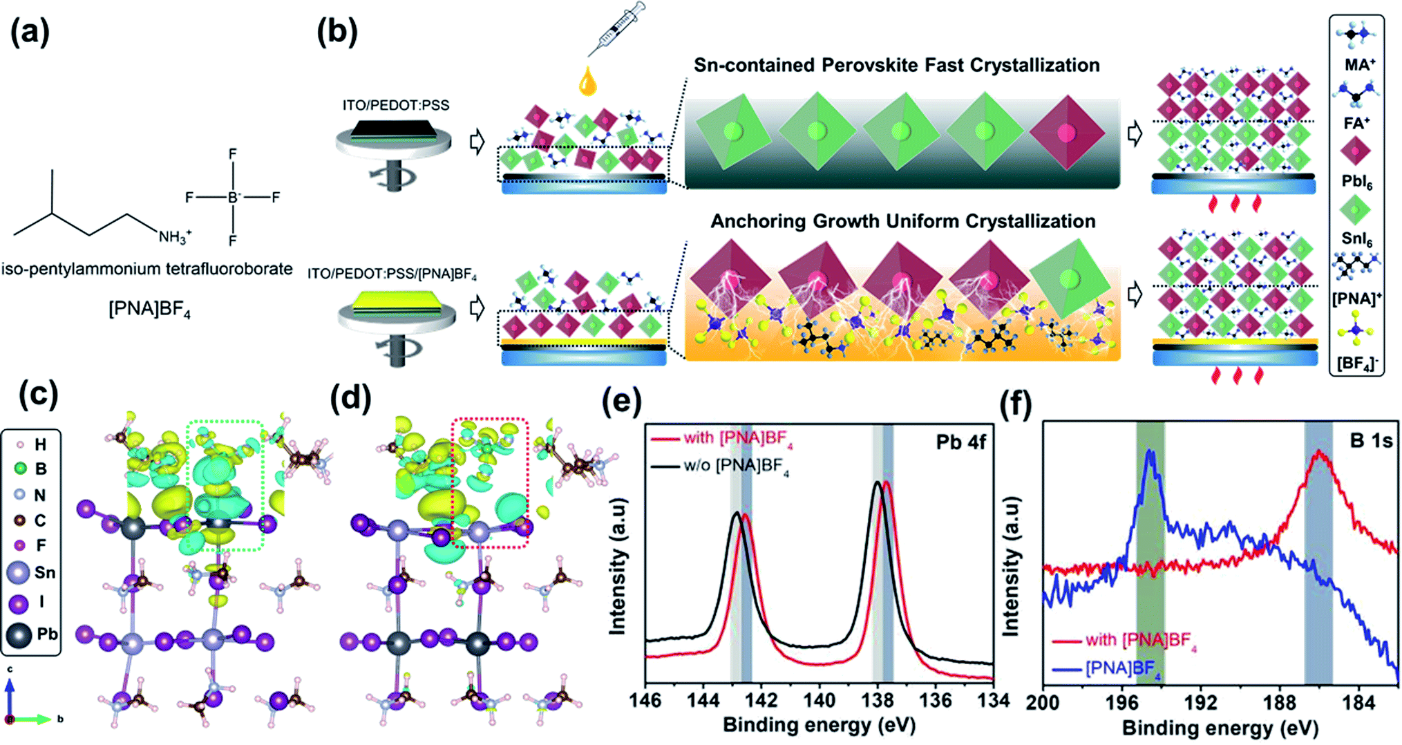 | ||
| Fig. 1 (a) The molecular structure of iso-pentylammonium tetrafluoroborate ionic salts; (b) the schematic illustration of [PNA]BF4 ionic substrates anchoring growth of mixed Sn–Pb perovskite; side view of 3D charge density differences of [PNA]BF4 molecular coupled to (c) Pb2+ or (d) Sn2+ and I− ion in MAPb0.5Sn0.5I3 models (yellow: gaining electron, cyan: electron deficit); XPS spectra of (e) Pb 4f for pristine and [PNA]BF4 doped perovskite film, (f) B 1s for [PNA]BF4 doped perovskite and pristine [PNA]BF4. | ||
To study the interaction between modified substrate and perovskite, we applied density functional theory (DFT) to simulate the chemical anchoring effect between [PNA]BF4 and MASn0.5Pb0.5I3. Fig. 1c and d display the optimized geometrical structure of [PNA]BF4 molecular coupled to Pb2+ or Sn2+ and I− ions in perovskite models. The charge density distribution plots uncovered that the electron cloud of the [BF4]− anion becomes more delocalized once contacted with Pb2+ while there is no charge transfer behavior occurring with Sn2+ (as shown in inset box), suggesting that the [BF4]− anion can have relatively stronger ionic interaction with Pb2+ compared to Sn2+. Besides, some cyan charge deficit can be found around [PNA]+ in Fig. 1d, since the chemical reducibility of ammonium (–NH3+) in [PNA]+ will transfer part of the charge to adjacent Sn2+ and inhibit its oxidation occurring near contacting interfaces.33,34 Furthermore, X-ray photoelectron spectroscopy (XPS) analysis was applied to verify these processes as shown in Fig. 1e, f, S1, S2, Tables S1 and S2.† Here, 10 mmol% [PNA]BF4 ionic salt was added in a mixed Sn–Pb perovskite precursor solution and the corresponding film along with control samples were taken in this measurement. After incorporating [PNA]BF4 ionic salts, a substantially reduced content of Sn4+ (from 63.72% to 27.56%, Fig. S1†) is presented along with a slightly increased binding energy of Sn 3d peaks (Table S1†). Meanwhile, Pb 4f7/2 and Pb 4f5/2 peaks are moved to lower binding energy values and binding energy of B 1s is shifted from 194.71 to 187.23 eV, while N 1s, especially ammonium (C–NH3+), remains unchanged after [PNA]BF4 was added. These data suggest that [BF4]− can preferentially anchor with Pb2+ by its ionic bonding in this mixed Sn–Pb perovskite film. We denote this effect as the chemical-anchoring effect in the later discussion. In parallel, [PNA]+ also shows to suppress Sn2+ oxidation, which is consistent with DFT calculation results. To further explore the interaction between [PNA]BF4 and PEDOT:PSS, the Fourier-transform infrared (FTIR) spectrum comparison was applied as shown in Fig. S3.† Original bands related to symmetric stretching (νa = 1190 cm−1) and antisymmetric stretching vibration (νas = 1140 cm−1) of S![[double bond, length as m-dash]](https://www.rsc.org/images/entities/char_e001.gif) O from –SO3− blue-shifted to 1170 and 1030 cm−1, while intrinsic –NH3+ group bands (νas = 3300 and 2960 cm−1) red-shifted to 3330 and 3030 cm−1, respectively.35,36 These observations can be ascribed to the decreasing spatial symmetry of SO3− after its coordination with –NH3+. In other words, [PNA]BF4 can suppress the hydrolysis of –SO3− by its NH3+ functional group and water-resistant long alkyl chains contained in [PNA]+. Additionally, XPS analyses were also performed to measure the pristine [PNA]BF4 films before and after washing with DMF:DMSO solvent as shown in Fig. S4.† Both results show the same N 1s and F 1s peaks belonging to the primary [PNA]+ cation and [BF4]− anion, respectively, which confirms that the DMF:DMSO solvent used in the perovskite precursor solution cannot wash away the pre-deposited [PNA]BF4 ionic salt layer. In the end, [PNA]BF4 is capable of encapsulating the acidic and hygroscopic PEDOT:PSS layer and improving the stability of mixed Sn–Pb perovskite films.
O from –SO3− blue-shifted to 1170 and 1030 cm−1, while intrinsic –NH3+ group bands (νas = 3300 and 2960 cm−1) red-shifted to 3330 and 3030 cm−1, respectively.35,36 These observations can be ascribed to the decreasing spatial symmetry of SO3− after its coordination with –NH3+. In other words, [PNA]BF4 can suppress the hydrolysis of –SO3− by its NH3+ functional group and water-resistant long alkyl chains contained in [PNA]+. Additionally, XPS analyses were also performed to measure the pristine [PNA]BF4 films before and after washing with DMF:DMSO solvent as shown in Fig. S4.† Both results show the same N 1s and F 1s peaks belonging to the primary [PNA]+ cation and [BF4]− anion, respectively, which confirms that the DMF:DMSO solvent used in the perovskite precursor solution cannot wash away the pre-deposited [PNA]BF4 ionic salt layer. In the end, [PNA]BF4 is capable of encapsulating the acidic and hygroscopic PEDOT:PSS layer and improving the stability of mixed Sn–Pb perovskite films.
To further examine the morphological information of the perovskite film surface, top view scanning electron microscopy (SEM) and atomic force microscopy (AFM) images of perovskite films grown on substrates with or without [PNA]BF4 treatment were acquired, as presented in Fig. 2a and c. The FA0.7MA0.3Pb0.5Sn0.5I3 film grown on [PNA]BF4 modified substrate exhibits a more compact and uniform structure with a larger grain size compared to that of control samples. Also, the corresponding statistics of perovskite grain size were calculated as shown in Fig. S5;† the average grain size significantly increases from 390 nm to 1050 nm and a more homogeneous distribution is gained from the [PNA]BF4 treatment. This phenomenon symbolizes the reduction of the grain-boundary energy and surface trap-state density.37,38 Furthermore, the cross-section morphology of these perovskites is shown in Fig. 2b and d. The control samples display deep cracks inside crystals, which can cause gaps and voids between the transporting layer and silver electrode (indicated by arrows in Fig. 2b). After growing [PNA]BF4 on substrates (Fig. 2d), the film shows a compact and dense morphology, in which, grains are uniformly expanded to several micrometers along with the substrates and along the vertical direction. More importantly, [PNA]BF4 forms a flat top surface and avoids contact gaps with the transporting layers, which is found to be different in control samples. From the data above, [PNA]BF4 treatment shows an excellent control of the internal grain growth and surface morphology of the mixed Sn–Pb perovskite film.
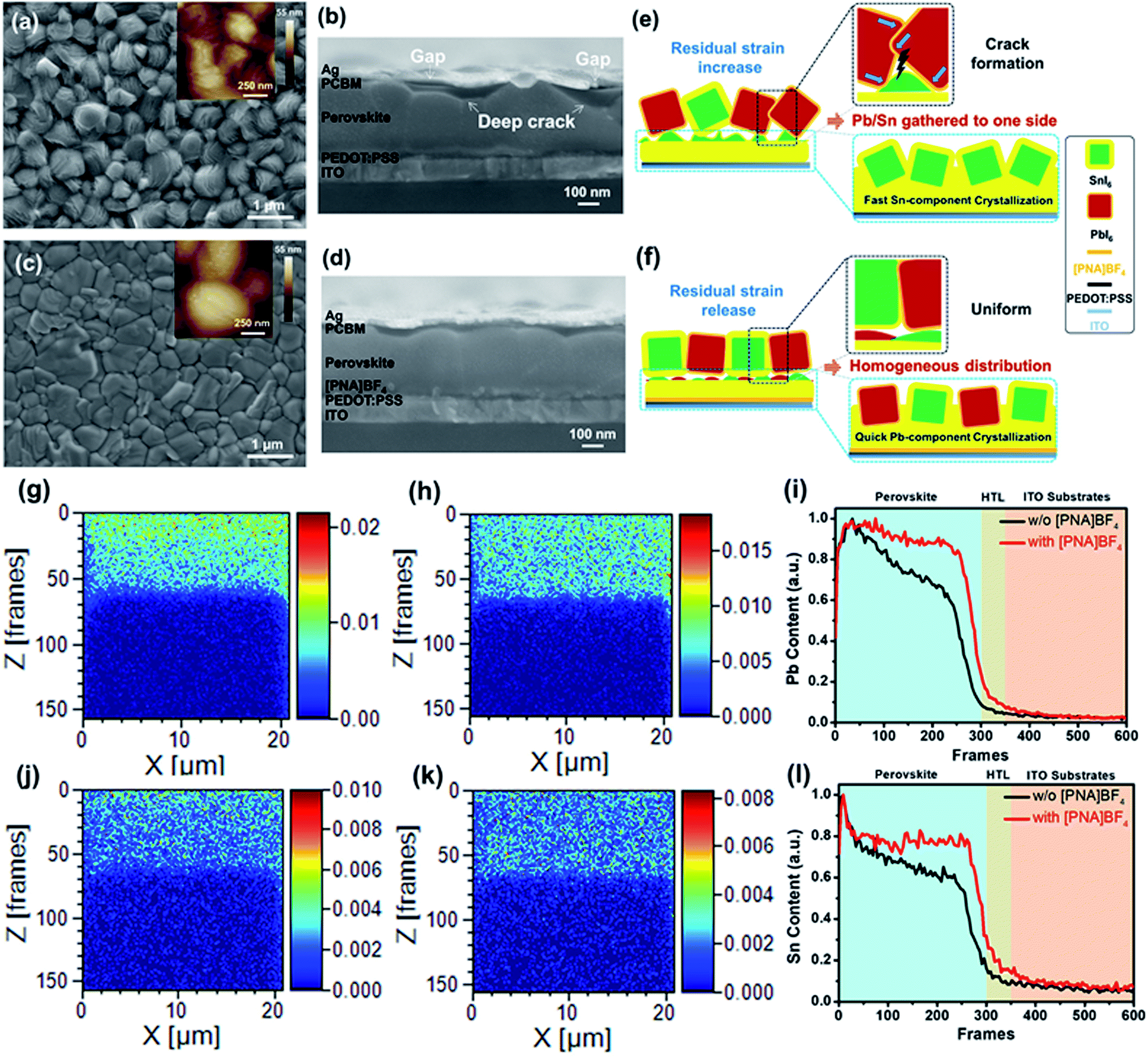 | ||
| Fig. 2 Top-view SEM and AFM images of (a) pristine and (b) [PNA]BF4 treated perovskite film; cross-section SEM images of (c) pristine devices and (d) [PNA]BF4 treated devices; the schematic illustration of perovskite films grown on (e) PEDOT:PSS and (f) [PNA]BF4 layer; TOF-SIMS mapping of Pb and Sn contents in the vertical direction during FIB etching frames from 0–150 for (g) and (j) pristine perovskite film grown on PEDOT:PSS/ITO, (h) and (k) the perovskite film grown on [PNA]BF4 modified PEDOT:PSS/ITO, respectively. The corresponding content profile of (i) Pb and (l) Sn in the vertical direction with the FIB etching frame from 0–600. | ||
To explain the formation of different film morphology, schematic illustrations are given in Fig. 2e and f. In control samples, when mixed Sn–Pb perovskite is deposited on the PEDOT:PSS substrate, the rapid precipitation of Sn-containing perovskites can disorderly expand in heterogeneous directions, pre-occupying the room that is available for the growth of Pb-contained perovskite. When Pb-containing perovskite begins to precipitate, the morphology of pre-existing Sn-contained perovskite needs to be re-organized in order to accommodate the growth of Pb-perovskite. As a result, a rough surface morphology, internal cracks, and large residual stress (Fig. 2e) are commonly found in the case of unbalanced crystallization rate between Sn–Pb perovskite. In comparison, when the mixed Sn–Pb perovskite is deposited on the [PNA]BF4/PEDOT:PSS substrate, [PNA]BF4 can induce a quick crystallization of Pb-contained perovskite by the chemical anchoring effect. Since the formation of both Sn- and Pb-perovskites are precipitating at the same pace, both components can have sufficient room to coagulate. Therefore, the resulting morphology of the film is compact without grain cracks. Based on these two different crystallization processes, there exist different Sn/Pb component distributions inside perovskite films.
To gain insight into the distribution of Sn/Pb-containing perovskite components inside these perovskite films, FIB TOF-SIMS mapping measurements were applied to characterize the chemical content of Pb and Sn elements in a vertical direction (or Z direction) of these film samples. Also, top-view SEM images of the final perovskite film after FIB etching are shown in Fig. S6.† In the control film, as presented in Fig. 2g and j, the Pb component is mainly gathered around the upper surface of the perovskite film (Fig. 2g), while the Sn component is slightly enriched in its middle or lower portion of the perovskite film (Fig. 2j). After incorporating the [PNA]BF4 layer, a homogeneous component distribution for both Pb and Sn elements is obtained inside the perovskite film, as shown in Fig. 2h and k. The corresponding normalized chemical content profiles of Pb and Sn elements in the vertical direction of these films are displayed in Fig. 2i and l, respectively. Compared to the control, there is less variation in Pb or Sn contents with different film depths after growing on [PNA]BF4 modified substrates. This observation confirms our hypothesis for the grain growth theory above. Furthermore, it also illustrates that the growth strategy assisted by the chemical-anchoring effect can give a significant improvement for the homogeneous distribution of Sn/Pb-containing perovskite inside films.
To further investigate the influence of different substrates on the crystallization process of perovskite film, the corresponding surface residual stress in these films was measured using an X-ray diffractometer (XRD). First, perovskite lattice plane patterns grown on [PNA]BF4 substrates with different coating concentrations were obtained, as shown in Fig. S7.† Among different samples, all results display the same diffraction peaks at the specific X-ray incident angles, manifesting the unitary perovskite phase with high crystallinity.39,40Fig. 3a is the magnified view of corresponding (110) peaks, the diffraction angles tend to gradually shift to lower values, which is signifying the change in film surface residual stress.41 Second, a well-established XRD sin2![[thin space (1/6-em)]](https://www.rsc.org/images/entities/char_2009.gif) ψ method was applied to quantitatively evaluate surface residual stress (σR) values in these perovskite films. There, typically exists biaxial residual stress (Φ = 0 and 90° orientations, corresponding to the lateral and longitude residual stress) in solution-processed perovskite films.42,43 In Fig. 3b and c, (110) interplanar spacing (d110) is plotted as a function of sin2ψ for control and perovskite films grown on [PNA]BF4 layer (0.5 mg mL−1), respectively. A negative slope of the linear fit to the d110–sin2ψ data indicates the presence of biaxial compressive surface residual stress in films. The resulting fitting lines of [PNA]BF4-treated perovskite films (Fig. 3c) show a lower negative slope compared to control samples (Fig. 3b), suggesting that the decrease in biaxial residual stress after the film growing on [PNA]BF4 substrate (0.5 mg mL−1). Similarly, the film biaxial σR values based on other coating concentrations of [PNA]BF4 substrates were estimated from the d110–sin2ψ data in Fig. S8.† All results are presented in Fig. 3d. The compressive σR for [PNA]BF4 samples are substantially reduced compared to the control (103 MPa for lateral stress, 114 MPa for longitude stress). The biaxial residual stress for the perovskite film treated with 0.2, 0.8, and 1.0 mg mL−1 [PNA]BF4 solutions decreases to 95, 79 and 92 MPa for lateral stress while 108, 91, and 104 MPa for longitude stress, respectively. Especially, the films grown on 0.5 mg mL−1 [PNA]BF4 substrate show the lowest biaxial residual stress (74 MPa for lateral stress, 83 MPa for longitude stress). Reduced residual stress in the surface region means the lattice distortion of perovskite has been mitigated. This also signifies fewer interface defects and traps in the perovskite film.44,45 Conclusively, the anchoring agents facilitate a homogeneous distribution of the Sn/Pb-containing perovskite component through a uniform crystallization process, which promotes the increment in perovskite grain size. This can be attributed to the elimination of lattice extrusion caused by the quick crystallization of the Sn-containing perovskite. As is well-known, the decrease in compressive residual stress of the perovskite film will increase the crystal lattice spacing, which means that the grain number in the same deposition area decreases while the grain size increases.46–48 In our results, the reduced compressive residual stress in [PNA]BF4 treated film makes the crystal lattice spacing increase, leading to the enlargement in grain size. This in turn is benefited from the uniform crystallization of Sn-/Pb-component perovskite crystals and promotes high crystalline quality of the perovskite film.
ψ method was applied to quantitatively evaluate surface residual stress (σR) values in these perovskite films. There, typically exists biaxial residual stress (Φ = 0 and 90° orientations, corresponding to the lateral and longitude residual stress) in solution-processed perovskite films.42,43 In Fig. 3b and c, (110) interplanar spacing (d110) is plotted as a function of sin2ψ for control and perovskite films grown on [PNA]BF4 layer (0.5 mg mL−1), respectively. A negative slope of the linear fit to the d110–sin2ψ data indicates the presence of biaxial compressive surface residual stress in films. The resulting fitting lines of [PNA]BF4-treated perovskite films (Fig. 3c) show a lower negative slope compared to control samples (Fig. 3b), suggesting that the decrease in biaxial residual stress after the film growing on [PNA]BF4 substrate (0.5 mg mL−1). Similarly, the film biaxial σR values based on other coating concentrations of [PNA]BF4 substrates were estimated from the d110–sin2ψ data in Fig. S8.† All results are presented in Fig. 3d. The compressive σR for [PNA]BF4 samples are substantially reduced compared to the control (103 MPa for lateral stress, 114 MPa for longitude stress). The biaxial residual stress for the perovskite film treated with 0.2, 0.8, and 1.0 mg mL−1 [PNA]BF4 solutions decreases to 95, 79 and 92 MPa for lateral stress while 108, 91, and 104 MPa for longitude stress, respectively. Especially, the films grown on 0.5 mg mL−1 [PNA]BF4 substrate show the lowest biaxial residual stress (74 MPa for lateral stress, 83 MPa for longitude stress). Reduced residual stress in the surface region means the lattice distortion of perovskite has been mitigated. This also signifies fewer interface defects and traps in the perovskite film.44,45 Conclusively, the anchoring agents facilitate a homogeneous distribution of the Sn/Pb-containing perovskite component through a uniform crystallization process, which promotes the increment in perovskite grain size. This can be attributed to the elimination of lattice extrusion caused by the quick crystallization of the Sn-containing perovskite. As is well-known, the decrease in compressive residual stress of the perovskite film will increase the crystal lattice spacing, which means that the grain number in the same deposition area decreases while the grain size increases.46–48 In our results, the reduced compressive residual stress in [PNA]BF4 treated film makes the crystal lattice spacing increase, leading to the enlargement in grain size. This in turn is benefited from the uniform crystallization of Sn-/Pb-component perovskite crystals and promotes high crystalline quality of the perovskite film.
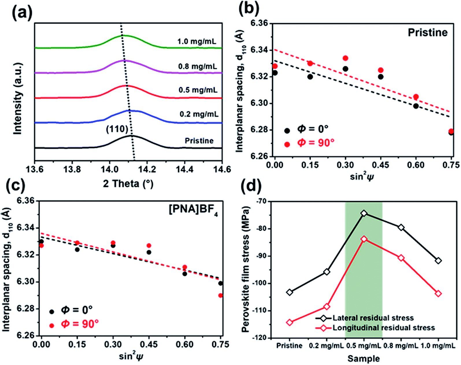 | ||
| Fig. 3 (a) XRD spectra of magnified (110) lattice plane diffraction peaks for perovskite films grown on PEDOT:PSS and different concentrations of the [PNA]BF4 layer; XRD d110versus sin2ψ plots for perovskite film grown on (b) PEDOT:PSS and (c) [PNA]BF4 layer (5 mg mL−1); (d) lateral and longitude residual stress (or strain) of perovskite films based on PEDOT:PSS and different concentration [PNA]BF4 layer. | ||
2.2 Device performance of Sn–Pb PSCs based on [PNA]BF4 treatment
After investigating the morphology and crystallization process of the mixed Sn–Pb perovskite grown on [PNA]BF4 substrates, we fabricated mixed Sn–Pb perovskite solar cells to evaluate the photovoltaic performance of the devices based on the [PNA]BF4 treatment. The architecture of the device is ITO/PEDOT:PSS/with or without [PNA]BF4/FA0.7MA0.3Pb0.5Sn0.5I3/PCBM/BCP/Ag is shown in Fig. 4a. The energy level positions related to the device are also measured by ultraviolet photoelectron spectroscopy (UPS) and are shown in Fig. S9–S12.† Tauc plots calculated from optical absorption spectra are displayed in Fig. S13 and S14.† Notably, as shown in Fig. 4b, the presence of [PNA]BF4 elevated the highest occupied molecular orbital (HOMO) of PEDOT:PSS from 5.02 eV to 5.22 eV, which is closer to the valence band maximum (VBM) of the mixed Sn–Pb perovskite in our work, suggesting the well-matched energy-level of each layer corresponding to this device. In addition, the atomic force microscopy (AFM) and Kelvin probe force microscope (KPFM) images in Fig. S21† show that the root mean square roughness (RMS) of PEDOT:PSS substrate after the [PNA]BF4 treatment is reduced from 1.87 to 1.54 nm, and the corresponding average surface potential distribution is decreased from 18.2 to 16.8 mV. These data indicate that the morphology and surface potential distribution of [PNA]BF4 treated substrates are more uniform compared to those of control, which could contribute to the reduction of interfacial non-radiative recombination and device performance improvement.49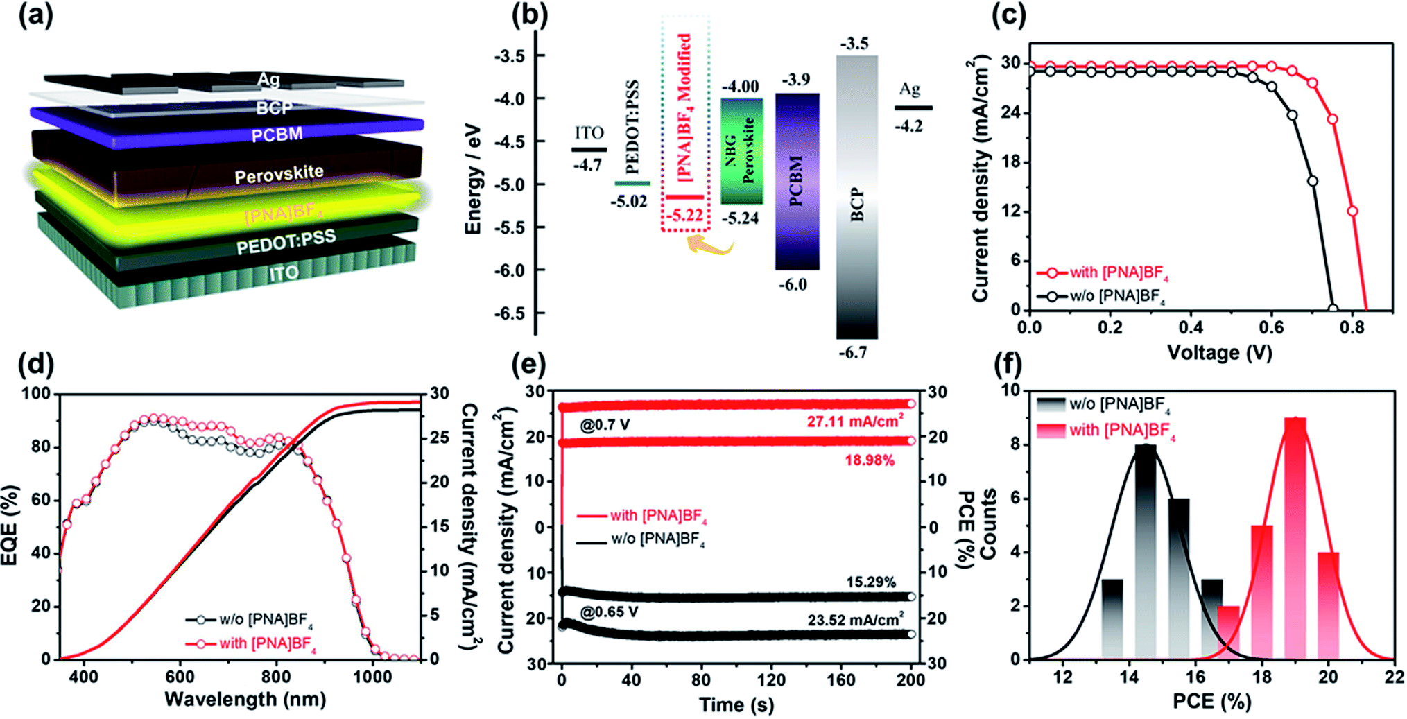 | ||
| Fig. 4 (a) The device structure of mixed Sn–Pb perovskite PSCs treated by [PNA]BF4 ionic salts; (b) energy-level diagram of each layer related devices; (c) J–V curves of champion PSCs under AM 1.5G 100 mW cm−2 illumination; (d) EQE spectra of corresponding PSCs; (e) steady-state Jsc and corresponding efficiencies of champion devices (at 0.70 V for the PSC with [PNA]BF4, at 0.65 V for the PSC without [PNA]BF4); (f) performance distribution diagram for 20 devices in one bath. | ||
The typical current density–voltage (J–V) curves of PSCs treated with different concentrations of [PNA]BF4 solutions are presented in Fig. S15,† and corresponding photovoltaic parameters are shown in Table S3.† Compared with the best PCE of 16.23% for the control device, the PCE of devices treated with 0.2 and 0.8 mg mL−1 [PNA]BF4 solutions increases to 18.11% and 19.02%, respectively. However, the high concentration [PNA]BF4 treatment process is harmful to the device's performance. When its concentration reaches 1.0 mg mL−1, the PCE of devices drops to 14.95%. The champion J–V curves of PSCs with and without [PNA]BF4 treatment are presented in Fig. 4c. The 0.5 mg mL−1 [PNA]BF4-treated PSCs show a reverse-scan PCE of 20.11% with a short-circuit current density (Jsc) of 29.69 mA cm−2, an open-circuit voltage (Voc) of 0.83 V and a fill factor (FF) of 81.62%. The forward scan of the same device shows a PCE of 19.78% with negligible hysteresis displayed in Fig. S16.† For comparison, the pristine device shows a reverse-scan PCE of 16.23% (Fig. 4c) and forward-scan PCE of 15.04% (Fig. S16†). The detailed photovoltaic parameters are given in Table S4.† The significant improvement in [PNA]BF4-treated device performance is mainly attributed to the higher Voc (increased from 0.75 V to 0.83 V) and FF (increased from 74.42% to 81.62%) compared to the control. The external quantum efficiency (EQE) and integrated current density Jsc of the [PNA]BF4 treated devices are presented in Fig. 4d. The integrated Jsc is 29.10 mA cm−2 in agreement with the Jsc obtained from J–V curves (29.69 mA cm−2). In addition, Fig. 4e shows the stabilized PCE of [PNA]BF4 treated and control devices measured at their fixed maximum power point (MPP) voltage, respectively. After exposure under continuous one-sun illustration for 200 s, the [PNA]BF4-treated device can still maintain a steady-state Jsc of 27.11 mA cm−2, corresponding to the stabilized PCE of 18.98%, which is much higher than that of the control device (15.29%). Besides, PCE histograms based on [PNA]BF4-treated and control devices for a sum of 20 devices are summarized in Fig. 4f. The corresponding photovoltaic parameters are displayed in Fig. S17,† [PNA]BF4-treated devices show enhanced device reproducibility. In sum, the devices based on [PNA]BF4 treatment show a notable improvement in photovoltaic performance and reproducibility.
In order to clarify the inherent mechanism of the superior photovoltaic performance in [PNA]BF4-treated devices, we first obtained transient absorption spectroscopy (TAS) in the picosecond domain to explore the ultrafast charge transfer and recombination mechanism in perovskite films. In Fig. 5a and b, the generation of ground-state bleaching (GSB) was detected in both pseudocolor TAS plots for the control and [PNA]BF4 treated perovskite films once evoked by the 500 nm pump pulse.50 As shown in Fig. 5c, the negative signals with a maximum amplitude of around 940 nm were featured in TAS spectra, which is assigned to the GSB, due to the state filling of conduction and valence bands.51 The intensity of the GSB signal is proportional to the charge densities and its dynamical evolution reflects the charge carrier dynamics.52 The initial GSB of perovskite film based on [PNA]BF4 is 15.89% higher than that of pristine perovskite. During the same decay time of 1 ns, the normalized decay ratio (ΔA) decreased to 18.87% for the control film, while a higher ratio of 28.91% was gained for the [PNA]BF4-treated one. Compared to the control perovskite, the [PNA]BF4-treated perovskite shows a much higher charge density and slower decay ratio. Furthermore, Fig. 5d shows the normalized transition dynamics of the decay time probed at the center of GSB (∼940 nm). The TAS decay spectra can be well fitted using a biexponential fitting model. The detailed parameters are listed in Table S5.† The kinetics fitting of the control film exhibits a short time constant of 42.72 ps and a long time constant of 526.45 ps and an average lifetime constant of 450.36 ps. In comparison, a much slower decay kinetic process with the three constants of 144.26 ps and 1237.71 ps and 1138.59 ps was fitted for the [PNA]BF4-treated perovskite. According to previous explanations of the ultrafast exciton trapping and recombination process, the fitted short lifetime (42.72 vs. 144.26 ps) belongs to the trapping of excitons by defects and the long lifetime (526.45 vs. 1237.71 ps) can be assigned to band-edge exciton recombination.53,54 The prolonged lifetime of the [PNA]BF4-treated perovskite film indicates a lower density of surface defects states, which leads to a reduced charge accumulation at this interface. In other words, this is direct evidence that the non-radiative recombination and surface defects are effectively suppressed in the [PNA]BF4-treated perovskite film. These observations are in agreement with the higher Voc of [PNA]BF4-treated devices compared to that of the control. Second, the steady-state photoluminescence (PL) spectra were further obtained to investigate carrier non-radiative recombination properties of these films, as presented in Fig. 5e. The control perovskites exhibit a typical emission peak at 1002 nm. After the [PNA]BF4 treatment, the intensity of this peak increases obviously. In particular, it triggered a 7 nm (from 1002 to 995 nm) blue shift of the steady-state PL peak, which means the carrier non-radiative recombination was significantly reduced and the defects were well eliminated. Time-resolved photoluminescence (TRPL) decay transient spectra were also applied to investigate the carrier lifetime inside these films (Fig. 5e). The same biexponential fitting model was used to fit these decay spectra. Detailed fitting information is listed in Table S6.† The fitted results prove that the average recombination lifetime prolonged from 1.93 to 6.91 ns (almost 3.5 times longer) after incorporating [PNA]BF4, which indicates that defect states or trap densities are substantially reduced. Third, the same results can be identified in the electrochemical impedance spectrum (EIS) (Fig. S18 and Table S7†), the carrier recombination resistance of PSCs based on [PNA]BF4 treatment has increased apparently due to suppressed defects or traps.
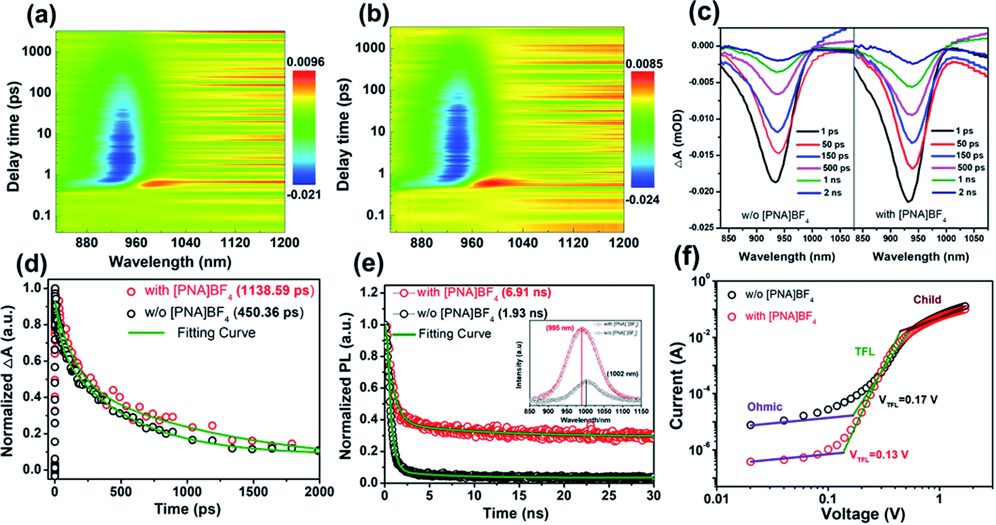 | ||
| Fig. 5 The pseudocolor TA spectrum plot of pristine perovskite film (a) and perovskite film grown on [PNA]BF4 layer (b); (c) the corrected femtosecond TA spectroscopy of corresponding perovskite films at selected probe delay times; (d) TA spectra as a function of delay time for corresponding perovskite film; (e) normalized TRPL decay transient spectra of perovskite grown on glass (without [PNA]BF4) and glass/[PNA]BF4 (with [PNA]BF4), inset: the related steady-state PL spectra; (f) hole-only devices for direct measurement of trap state densities. | ||
To further confirm the change of defect states or trap densities in perovskite films, the space charge limited current (SCLC) measurement is presented in Fig. 5f, in which hole-only devices structured as ITO/PEDOT:PSS/with or without [PNA]BF4/FA0.7MA0.3Pb0.5Sn0.5I3/PTAA/Ag were fabricated. The calculated trap densities (ntrap) of devices based on control perovskite and [PNA]BF4 treatment were 2.63 × 1015 cm−3 and 2.01 × 1015 cm−3, respectively. The reduced ntrap in [PNA]BF4-treated devices indicates that this growth strategy can effectively reduce the defects on the perovskite surface, contributing to the Voc enhancement of devices. The saturation dark current density (J0) for these integrated PSCs is further measured to evaluate the charge recombination according to the diode law.55,56 In Fig. S19,† the J0 of control and [PNA]BF4 treated devices are 6.20 × 10⁻⁶ mA cm−2 and 2.29 × 10⁻⁴ mA cm−2, respectively. The two orders of magnitude reduction in the J0 of [PNA]BF4-treated devices can further represent an effectively suppressed charge recombination in the perovskite film, which can also contribute to an enhanced Voc in device performance. Consequently, all these observations have manifested that the [PNA]BF4 treatment can passivate and reduce the trap states of the Sn–Pb perovskite layer effectively via the control of Sn–Pb grain growth, resulting in high photovoltaic performance.
2.3 Thermal and shelf storage stability of mixed Sn–Pb PSCs
Apart from efficiency, stability is also an important parameter in evaluating device performance. We first examine the water contact angles to investigate the hydrophobicity of different substrates, as shown in Fig. S20.† The PEDOT:PSS substrates have the lowest contact angle of 10.8°. After 0.2, 0.5, 0.8 and 1.0 mg mL−1 [PNA]BF4 treatments, the water contact angles increase to 31.3°, 40.6°, 47.1° and 53.7° (Fig. S19†), respectively. The substrates based on [PNA]BF4 treatment show an increment in water contact angles due to the [PNA]BF4 molecule with a long alkyl chain on the PEDOT:PSS surface, which can effectively prevent H2O from the hygroscopic PEDOT:PSS, leading to enhanced device stability. There is no change in the surface morphology of PEDOT:PSS after modification with [PNA]BF4, as presented in Fig. S21.†In order to further investigate the potential of Sn–Pb perovskite solar cells in real applications, thermal and shelf storage stability testings were performed. All samples were stored in dark to eliminate the light degradation effect on perovskite materials, and the device performance test process was carried out in ambient air (Rh = 30 ± 5%, T = 25 °C).57–59 In the thermal stability testing of mixed Sn–Pb PSCs, the unencapsulated PSCs were aged on an 85 °C hotplate in a nitrogen glovebox (H2O < 0.1 ppm, O2 < 0.1 ppm) for 240 h, as shown from the data in Fig. 6a. The previous report shows that the thermal stability of (FASnI3)0.6(MAPbI3)0.4 based PSCs was less than 40% of its initial efficiency after aging for 120 h.60 In this case of fast degradation, the degradation factor is likely to be the interfacial problem, which is the acidic PEDOT:PSS.60 Here, our device based on the [PNA]BF4 treatment can retain more than 80% of its initial efficiency for 240 h, while the control device can only retain 20% of its initial performance. This result shows the effectiveness of the chemical encapsulation strategy on PEDOT:PSS to improve thermal stability at the interface. Next, the data on tests on shelf storage stability without encapsulation in nitrogen glovebox (maintained around 25 °C) for 1200 h are provided in Fig. 6b. The recently reported shelf-storage stability of the FA0.5MA0.5Pb0.5Sn0.5I3-based PSCs is about 70% of its initial efficiency after aging for 1000 h. In the storage testing and slow degradation regime, the main degradation usually comes from internal factors, such as unstable Sn-contained perovskite components.61 Here, our device treated by [PNA]BF4 can retain over 90% of its initial PCE for 1200 h, which is much higher than that of control devices with a 20% retaining rate. One possible reason for the fast degradation in the control film can be ascribed to the accumulation of Sn-contained perovskite near the bottom interface due to the unregulated crystallization process. In the case of [PNA]BF4 treated devices, the distribution of the Sn/Pb component is homogeneous in the vertical direction of perovskite films. We believe that this homogeneous distribution of the Sn/Pb component can relatively reduce the chance of Sn2+ content being degraded at the interface. From FTIR characterization, as shown in Fig. S2,† the reactive sulfonic acid groups (–SO3H) from PEDOT:PSS molecule can be chemically neutralized by ammonium (–NH4+) contained in [PNA]BF4 molecule, thus preventing the irreversible degradation reaction between PEDOT:PSS and mixed Sn–Pb perovskite. Consequently, significant improvement of stability is originated from both balanced crystallization rate and chemically encapsulated PEDOT:PSS substrate.
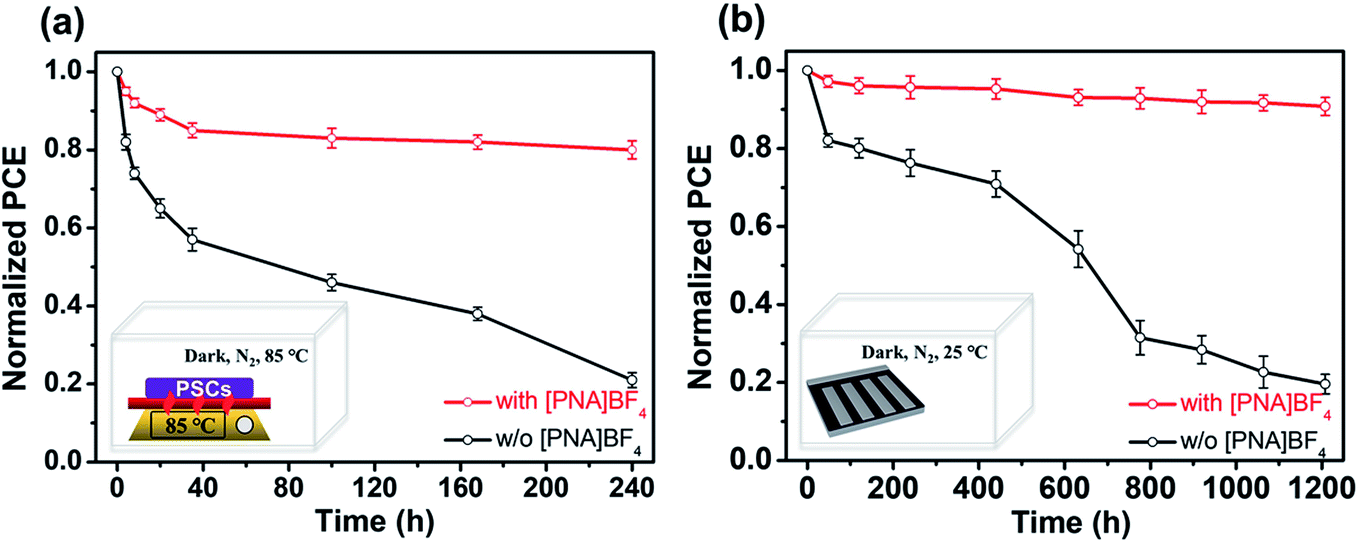 | ||
| Fig. 6 (a) Thermal and (b) shelf stability of PSCs devices with or without [PNA]BF4 treatment. | ||
3. Conclusion
In conclusion, we have realized the vertically homogeneous distribution of Sn/Pb-contained perovskite films by balancing the crystallization rate between Sn- and Pb-contained perovskite. The introduced ionic molecule, [PNA]BF4, on the PEDOT:PSS substrate can function as chemical anchoring agents to bond Pb2+ to the surface of PEDOT:PSS and facilitate a quick deposition of Pb-contained perovskite. Benefiting from this balanced crystallization rate and grain growth process, greatly reduced surface residual stress and decreased defect state densities are realized in the [PNA]BF4-treated perovskite films. Additionally, this [PNA]BF4 molecule can chemically encapsulate the acidic PEDOT:PSS substrate and prevent it from reacting with mixed Sn–Pb perovskite, thus greatly improving the device's stability. As a result, the optimized device shows an encouraging PCE of 20.11% with increasing Voc (from 0.75 V to 0.83 V) and FF (from 74.42% to 81.62%). Furthermore, both thermal and shelf storage stability of devices are greatly improved owing to both encapsulation effect at the interface and crystallization control effect in the bulk perovskite provided by [PNA]BF4 treatment. In short, by balancing the crystallization rate in multi-component halide perovskite, e.g. mixed Sn–Pb perovskite, significant improvements in both efficiency and stability are observed for PSCs, making this new kind of mixed perovskite system one step closer to the practical applications and commercialization.Author contributions
C. C. and Z. Z. designed the research. Z. Z., J. W., Y. H., Y. Y. and Z. Z. prepared the samples and took the measurements of the SEM, AFM, FTIR, PL, TRPL, XPS and UPS. Z. Z., J. L. and C. Q. performed the fs-TA measurements. Z. Z. and Y. Z. performed the surface residual stress (or strain) measurements. Z. Z. and X. W. performed the TOF-SIMS measurements. Z. Z. and L. W. and L. K. performed the DFT calculations. Z. Z. fabricated the devices and carried out the photovoltaic performance tests. Z. Z. and C. C. wrote the manuscript, with contributions from the other authors. C. C. and K. R. guided the projects.Conflicts of interest
There are no conflicts to declare.Acknowledgements
This study was funded partly by the National Natural Science Foundation of China (Grant No. 51950410581), the Shanghai Government (20JC141500) and the Shanghai Pujiang Program. We acknowledged The Instrumental Analysis Center of Shanghai Jiao Tong University for providing XPS and TOF-SIMS analysis. We are grateful for the discussion about the XPS data reduction with Ms Limin Sun, Ms Xue Ding and Ms Nannan Zhang, and the FIB TOF-SIMS data results with Ms Yao Han in The Instrumental Analysis Center of Shanghai Jiao Tong University. We would like to thank Chongfeng Zhong from Shiyanjia Lab (https://www.shiyanjia.com) for the Surface Residual Stress (Or Strain) Measurements.Notes and references
- NREL, Best Research-Cell Efficiency Chart, https://www.nrel.gov/pv/cell-efficiency.html Search PubMed.
- M. Green, E. Dunlop, J. Hohl-Ebinger, M. Yoshita, N. Kopidakis and X. Hao, Prog. Photovoltaics Res. Appl., 2021, 29, 3–15 CrossRef.
- W. Shockley and H. J. Queisser, J. Appl. Phys., 1961, 32, 510–519 CrossRef CAS.
- K. Xiao, R. Lin, Q. Han, Y. Hou, Z. Qin, H. T. Nguyen, J. Wen, M. Wei, V. Yeddu, M. I. Saidaminov, Y. Gao, X. Luo, Y. Wang, H. Gao, C. Zhang, J. Xu, J. Zhu, E. H. Sargent and H. Tan, Nat. Energy, 2020, 5, 870–880 CrossRef CAS.
- Q. Jiang, Y. Zhao, X. Zhang, X. Yang, Y. Chen, Z. Chu, Q. Ye, X. Li, Z. Yin and J. You, Nat. Photonics, 2019, 13, 460–466 CrossRef CAS.
- M. Wei, K. Xiao, G. Walters, R. Lin, Y. Zhao, M. I. Saidaminov, P. Todorović, A. Johnston, Z. Huang, H. Chen, A. Li, J. Zhu, Z. Yang, Y. Wang, A. H. Proppe, S. O. Kelley, Y. Hou, O. Voznyy, H. Tan and E. H. Sargent, Adv. Mater., 2020, 32, 1907058 CrossRef CAS.
- H. Kang and W. Yoon, Mater. Trans., 2004, 45, 2956–2959 CrossRef CAS.
- Y. Yu, C. Wang, C. R. Grice, N. Shrestha, J. Chen, D. Zhao, W. Liao, A. J. Cimaroli, P. J. Roland, R. J. Ellingson and Y. Yan, ChemSusChem, 2016, 9, 3288–3297 CrossRef CAS.
- R. Prasanna, A. Gold-Parker, T. Leijtens, B. Conings, A. Babayigit, H. G. Boyen, M. F. Toney and M. D. McGehee, J. Am. Chem. Soc., 2017, 139, 11117–11124 CrossRef CAS PubMed.
- Z. Ni, C. Bao, Y. Liu, Q. Jiang, W. Q. Wu, S. Chen, X. Dai, B. Chen, B. Hartweg, Z. Yu, Z. Holman and J. Huang, Science, 2020, 367, 1352–1358 CrossRef CAS.
- J. Tong, Z. Song, D. H. Kim, X. Chen, C. Chen, A. F. Palmstrom, P. F. Ndione, M. O. Reese, S. P. Dunfield, O. G. Reid, J. Liu, F. Zhang, S. P. Harvey, Z. Li, S. T. Christensen, G. Teeter, D. Zhao, M. M. Al-Jassim, M. F. A. M. Van Hest, M. C. Beard, S. E. Shaheen, J. J. Berry, Y. Yan and K. Zhu, Science, 2019, 364, 475–479 CrossRef CAS.
- W. Ke and M. G. Kanatzidis, Nat. Commun., 2019, 10, 1–4 CrossRef CAS.
- I. Chung, J. H. Song, J. Im, J. Androulakis, C. D. Malliakas, H. Li, A. J. Freeman, J. T. Kenney and M. G. Kanatzidis, J. Am. Chem. Soc., 2012, 134, 8579–8587 CrossRef CAS.
- Z. Yang, Z. Yu, H. Wei, X. Xiao, Z. Ni, B. Chen, Y. Deng, S. N. Habisreutinger, X. Chen, K. Wang, J. Zhao, P. N. Rudd, J. J. Berry, M. C. Beard and J. Huang, Nat. Commun., 2019, 10, 1–9 CrossRef.
- S. Shao, J. Dong, H. Duim, G. H. Ten Brink, G. R. Blake, G. Portale and M. A. Loi, Nano Energy, 2019, 60, 810–816 CrossRef CAS.
- D. H. Cao, C. C. Stoumpos, T. Yokoyama, J. L. Logsdon, T. Bin Song, O. K. Farha, M. R. Wasielewski, J. T. Hupp and M. G. Kanatzidis, ACS Energy Lett., 2017, 2, 982–990 CrossRef CAS.
- Y. Liao, H. Liu, W. Zhou, D. Yang, Y. Shang, Z. Shi, B. Li, X. Jiang, L. Zhang, L. N. Quan, R. Quintero-Bermudez, B. R. Sutherland, Q. Mi, E. H. Sargent and Z. Ning, J. Am. Chem. Soc., 2017, 139, 6693–6699 CrossRef CAS.
- Q. Li, Y. Dong, G. Lv, T. Liu, D. Lu, N. Zheng, X. Dong, Z. Xu, Z. Xie and Y. Liu, ACS Energy Lett., 2021, 6, 2072–2080 CrossRef CAS.
- G. Lv, L. Li, D. Lu, Z. Xu, Y. Dong, Q. Li, Z. Chang, W.-J. Yin and Y. Liu, Nano Lett., 2021, 21, 5788–5797 CrossRef CAS PubMed.
- X. Lian, J. Chen, Y. Zhang, M. Qin, J. Li, S. Tian, W. Yang, X. Lu, G. Wu and H. Chen, Adv. Funct. Mater., 2019, 29, 1807024 CrossRef.
- D. Yang, X. Zhou, R. Yang, Z. Yang, W. Yu, X. Wang, C. Li, S. Liu and R. P. H. Chang, Energy Environ. Sci., 2016, 9, 3071–3078 RSC.
- P. M. Hangoma, I. Shin, H. Yang, D. Kim, Y. K. Jung, B. R. Lee, J. H. Kim, K. H. Kim and S. H. Park, Adv. Funct. Mater., 2020, 30, 2003081 CrossRef CAS.
- J. Cameron and P. J. Skabara, Mater. Horiz., 2020, 7, 1759–1772 RSC.
- S. Gu, R. Lin, Q. Han, Y. Gao, H. Tan and J. Zhu, Adv. Mater., 2020, 32, 1907392 CrossRef CAS.
- C. Ionescu-Zanetti, A. Mechler, S. A. Carter and R. Lal, Adv. Mater., 2004, 16, 385–389 CrossRef CAS.
- R. Prasanna, T. Leijtens, S. P. Dunfield, J. A. Raiford, E. J. Wolf, S. A. Swifter, J. Werner, G. E. Eperon, C. de Paula, A. F. Palmstrom, C. C. Boyd, M. F. A. M. van Hest, S. F. Bent, G. Teeter, J. J. Berry and M. D. McGehee, Nat. Energy, 2019, 4, 939–947 CrossRef CAS.
- F. Hao, C. C. Stoumpos, P. Guo, N. Zhou, T. J. Marks, R. P. H. Chang and M. G. Kanatzidis, J. Am. Chem. Soc., 2015, 137, 11445–11452 CrossRef CAS PubMed.
- L. Wang, X. Wang, L. L. Deng, S. Leng, X. Guo, C. H. Tan, W. C. H. Choy and C. C. Chen, Mater. Horiz., 2020, 7, 934–942 RSC.
- C. Li, Z. Song, C. Chen, C. Xiao, B. Subedi, S. P. Harvey, N. Shrestha, K. K. Subedi, L. Chen, D. Liu, Y. Li, Y. W. Kim, C. Sheng Jiang, M. J. Heben, D. Zhao, R. J. Ellingson, N. J. Podraza, M. Al-Jassim and Y. Yan, Nat. Energy, 2020, 5, 768–776 CrossRef CAS.
- Y. Takahashi, R. Obara, Z. Z. Lin, Y. Takahashi, T. Naito, T. Inabe, S. Ishibashi and K. Terakura, Dalton Trans., 2011, 40, 5563–5568 RSC.
- Y. H. Lin, N. Sakai, P. Da, J. Wu, H. C. Sansom, A. J. Ramadan, S. Mahesh, J. Liu, R. D. J. Oliver, J. Lim, L. Aspitarte, K. Sharma, P. K. Madhu, A. B. Morales-Vilches, P. K. Nayak, S. Bai, F. Gao, C. R. M. Grovenor, M. B. Johnston, J. G. Labram, J. R. Durrant, J. M. Ball, B. Wenger, B. Stannowski and H. J. Snaith, Science, 2020, 369, 96–102 CrossRef CAS.
- X. Deng, L. Xie, S. Wang, C. Li, A. Wang, Y. Yuan, Z. Cao, T. Li, L. Ding and F. Hao, Chem. Eng. J., 2020, 398, 125594 CrossRef CAS.
- M. He, J. Liang, Z. Zhang, Y. Qiu, Z. Deng, H. Xu, J. Wang, Y. Yang, Z. Chen and C. C. Chen, J. Mater. Chem. A, 2020, 8, 25831–25841 RSC.
- J. J. Yoo, S. Wieghold, M. C. Sponseller, M. R. Chua, S. N. Bertram, N. T. P. Hartono, J. S. Tresback, E. C. Hansen, J. P. Correa-Baena, V. Bulović, T. Buonassisi, S. S. Shin and M. G. Bawendi, Energy Environ. Sci., 2019, 12, 2192–2199 RSC.
- R. Valentin, R. Horga, B. Bonelli, E. Garrone, F. Di Renzo and F. Quignard, Biomacromolecules, 2006, 7, 877–882 CrossRef CAS PubMed.
- L. Andrews, S. R. Davis and G. L. Johnson, J. Phys. Chem., 1986, 90, 4273–4282 CrossRef CAS.
- W. Chen, J. Zhang, G. Xu, R. Xue, Y. Li, Y. Zhou, J. Hou and Y. Li, Adv. Mater., 2018, 30, 1800855 CrossRef.
- Z. Liu, J. Hu, H. Jiao, L. Li, G. Zheng, Y. Chen, Y. Huang, Q. Zhang, C. Shen, Q. Chen and H. Zhou, Adv. Mater., 2017, 29, 1606774 CrossRef.
- G. Kapil, T. S. Ripolles, K. Hamada, Y. Ogomi, T. Bessho, T. Kinoshita, J. Chantana, K. Yoshino, Q. Shen, T. Toyoda, T. Minemoto, T. N. Murakami, H. Segawa and S. Hayase, Nano Lett., 2018, 18, 3600–3607 CrossRef CAS PubMed.
- T. M. Koh, T. Krishnamoorthy, N. Yantara, C. Shi, W. L. Leong, P. P. Boix, A. C. Grimsdale, S. G. Mhaisalkar and N. Mathews, J. Mater. Chem. A, 2015, 3, 14996–15000 RSC.
- N. Yang, C. Zhu, Y. Chen, H. Zai, C. Wang, X. Wang, H. Wang, S. Ma, Z. Gao, X. Wang, J. Hong, Y. Bai, H. Zhou, B. Bin Cui and Q. Chen, Energy Environ. Sci., 2020, 13, 4344–4352 RSC.
- S. Jariwala, H. Sun, G. W. P. Adhyaksa, A. Lof, L. A. Muscarella, B. Ehrler, E. C. Garnett and D. S. Ginger, Joule, 2019, 3, 3048–3060 CrossRef CAS.
- Y. Chen, Y. Lei, Y. Li, Y. Yu, J. Cai, M. H. Chiu, R. Rao, Y. Gu, C. Wang, W. Choi, H. Hu, C. Wang, Y. Li, J. Song, J. Zhang, B. Qi, M. Lin, Z. Zhang, A. E. Islam, B. Maruyama, S. Dayeh, L. J. Li, K. Yang, Y. H. Lo and S. Xu, Nature, 2020, 577, 209–215 CrossRef CAS PubMed.
- H. Wang, C. Zhu, L. Liu, S. Ma, P. Liu, J. Wu, C. Shi, Q. Du, Y. Hao, S. Xiang, H. Chen, P. Chen, Y. Bai, H. Zhou, Y. Li and Q. Chen, Adv. Mater., 2019, 31, 1904408 CrossRef CAS PubMed.
- C. Zhu, X. Niu, Y. Fu, N. Li, C. Hu, Y. Chen, X. He, G. Na, P. Liu, H. Zai, Y. Ge, Y. Lu, X. Ke, Y. Bai, S. Yang, P. Chen, Y. Li, M. Sui, L. Zhang, H. Zhou and Q. Chen, Nat. Commun., 2019, 10, 1–11 CrossRef.
- M. X. Yang, R. G. Li, P. Jiang, F. P. Yuan, Y. D. Wang, Y. T. Zhu and X. L. Wu, Mater. Res. Lett., 2019, 7, 433–438 CrossRef CAS.
- K. Bobzin, W. Wietheger, M. A. Knoch, A. Schacht, U. Reisgen, R. Sharma and L. Oster, J. Therm. Spray Technol., 2020, 29, 1218–1228 CrossRef CAS.
- W. Węglewski, M. Basista, A. Manescu, M. Chmielewski, K. Pietrzak and T. Schubert, Composites, Part B, 2014, 67, 119–124 CrossRef.
- G. Xu, P. Bi, S. Wang, R. Xue, J. Zhang, H. Chen, W. Chen, X. Hao, Y. Li and Y. Li, Adv. Funct. Mater., 2018, 28, 1804427 CrossRef.
- W. Xu, Y. Gao, W. Ming, F. He, J. Li, X. Zhu, F. Kang, J. Li and G. Wei, Adv. Mater., 2020, 32, 2003965 CrossRef CAS PubMed.
- G. Xing, N. Mathews, S. Sun, S. S. Lim, Y. M. Lam, M. Gratzel, S. Mhaisalkar and T. C. Sum, Science, 2013, 342, 344–347 CrossRef CAS.
- S. Ravishankar, S. Gharibzadeh, C. Roldán-Carmona, G. Grancini, Y. Lee, M. Ralaiarisoa, A. M. Asiri, N. Koch, J. Bisquert and M. K. Nazeeruddin, Joule, 2018, 2, 788–798 CrossRef CAS.
- N. Mondal and A. Samanta, Nanoscale, 2017, 9, 1878–1885 RSC.
- Y. Wu, C. Wei, X. Li, Y. Li, S. Qiu, W. Shen, B. Cai, Z. Sun, D. Yang, Z. Deng and H. Zeng, ACS Energy Lett., 2018, 3, 2030–2037 CrossRef CAS.
- P. Singh and N. M. Ravindra, Sol. Energy Mater. Sol. Cells, 2012, 101, 36–45 CrossRef CAS.
- C. Li, Z. Song, D. Zhao, C. Xiao, B. Subedi, N. Shrestha, M. M. Junda, C. Wang, C.-S. Jiang, M. Al-Jassim, R. J. Ellingson, N. J. Podraza, K. Zhu and Y. Yan, Adv. Energy Mater., 2019, 9, 1803135 CrossRef.
- J. Wei, Q. Wang, J. Huo, F. Gao, Z. Gan, Q. Zhao and H. Li, Adv. Energy Mater., 2021, 11, 2002326 CrossRef CAS.
- Y. B. Lu, W. Y. Cong, C. Guan, H. Sun, Y. Xin, K. Wang and S. Song, J. Mater. Chem. A, 2019, 7, 27469–27474 RSC.
- S. Ruan, M. A. Surmiak, Y. Ruan, D. P. McMeekin, H. Ebendorff-Heidepriem, Y. B. Cheng, J. Lu and C. R. McNeill, J. Mater. Chem. C, 2019, 7, 9326–9334 RSC.
- C. Li, Z. Song, C. Chen, C. Xiao, B. Subedi, S. P. Harvey, N. Shrestha, K. K. Subedi, L. Chen, D. Liu, Y. Li, Y. W. Kim, C. Sheng Jiang, M. J. Heben, D. Zhao, R. J. Ellingson, N. J. Podraza, M. Al-Jassim and Y. Yan, Nat. Energy, 2020, 5, 768–776 CrossRef CAS.
- H. Kim, J. W. Lee, G. R. Han, S. K. Kim and J. H. Oh, Adv. Funct. Mater., 2021, 31, 2008801 CrossRef CAS.
Footnote |
| † Electronic supplementary information (ESI) available. See DOI: 10.1039/d1ta04922d |
| This journal is © The Royal Society of Chemistry 2021 |