
 Open Access Article
 This Open Access Article is licensed under a
 Creative Commons Attribution 3.0 Unported Licence
Optoelectronic devices based on the integration of halide perovskites with silicon-based materials
Jingjing
Liu
ab,
Junle
Qu
 a,
Thomas
Kirchartz
*bc and
Jun
Song
*a
a,
Thomas
Kirchartz
*bc and
Jun
Song
*a
aCenter for Biomedical Optics and Photonics (CBOP), College of Physics and Optoelectronic Engineering, Key Laboratory of Optoelectronic Devices and Systems, Shenzhen University, 518060 Shenzhen, P. R. China. E-mail: songjun@szu.edu.cn
bIEK5-Photovoltaics, Forschungszentrum Jülich, 52425 Jülich, Germany. E-mail: t.kirchartz@fz-juelich.de
cFaculty of Engineering and CENIDE, University of Duisburg-Essen, Carl-Benz-Strasse 199, 47057 Duisburg, Germany
First published on 26th August 2021
Abstract
Halide perovskites are widely used as an absorbing or emitting layer in emerging high-performance optoelectronic devices due to their high absorption coefficients, long charge carrier diffusion lengths, low defect density and intense photoluminescence. Si-based materials (c-Si, a-Si, SixNy, SiCx and SiO2) play important roles in high performance perovskite optoelectronic devices due to the dominance of Si-based microelectronics and the important role of Si-based solar cells in photovoltaics. Controlling the preparation of perovskite materials on the dominant Si optoelectronics platform is a crucial step to realize practical perovskite-based optoelectronic devices. This review highlights the recent progress in Si-based perovskite optoelectronic devices including perovskite/Si tandem solar cells, perovskite/Si photodetectors, perovskite/Si light emitting diodes and optically pumped lasers. The remaining challenge in Si-based perovskite optoelectronic devices research are discussed.
 Jingjing Liu | Jingjing Liu obtained her M.S. degree from Henan University in 2016 and PhD degree from the Nanjing University in 2019. She subsequently joined Shenzhen University as a postdoctoral researcher. She is currently a Visiting Scholar with Professor Thomas Kirchartz at the Research Centre Jülich (Institute for Energy and Climate Research), Germany. Her research interests are semiconductor self-assembled monolayer materials and their applications in perovskite solar cells. |
 Junle Qu | Junle Qu is currently the dean of the College of Optoelectronic Engineering and the director of the Key Laboratory of Optoelectronic Devices and Systems of the Education Ministry, Shenzhen University. He is an SPIE fellow member and the chairman of the Biomedical Photonics Specialized Committee of the Chinese Optical Society. His research focuses on fluorescence lifetime imaging, NIR-II imaging, super-resolution imaging, etc. He is leading 15 research projects, including the National Outstanding Youth Fund Project of China, the National Plan on Key Basic Research and Development, etc. |
 Thomas Kirchartz | Thomas Kirchartz is currently a professor of electrical engineering and information technology at the University Duisburg-Essen and the head of the Department of Analytics and Simulation and the group of organic and hybrid solar cells at the Research Centre Jülich (Institute for Energy and Climate Research). Previously, he was a Junior Research Fellow at Imperial College London. His research interests include all aspects regarding the fundamental understanding of photovoltaic devices including their characterization and simulation. |
 Jun Song | Jun Song received his B.Eng. degree in information engineering from Zhejiang University. Then, he received his PhD degrees from Zhejiang University and Royal Institute of Technology, respectively. He is currently a Professor of Biomedical Photonics & College of Physics and Optoelectronic Engineering, Shenzhen University. His currently research focus on nanophotonics as well as its applications in renewable energy, biomedicine, electronic information, and environmental protection. |
1 Introduction
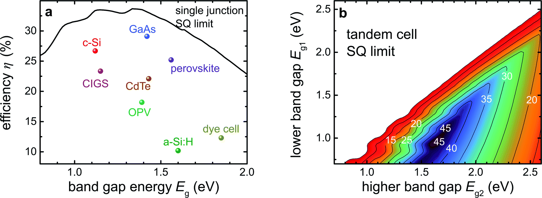
Silicon has been the cornerstone of microelectronics and photovoltaics (PV) for decades and is thereby central to the key technologies of digitalization and renewable energies that will shape the 21st century.1–3 Silicon has a multitude of advantages with the most important being our ability to grow huge monocrystalline Si crystals with excellent electronic properties, a near-perfect band gap for photovoltaics and a native oxide that protects the surface rather than making it rust like iron. There are only few disadvantages of silicon and they are related to the indirect nature of its band gap. The indirect band gap slows down radiative recombination and therefore makes it impossible to achieve Si-based light emitting diodes with a similar luminescence quantum efficiency as those made from III–V semiconductors such as GaAs.4–6 In addition, the indirect band gap reduces the absorption coefficient and therefore has prohibited the fabrication of highly efficient thin-film silicon solar cells. However, for the field of photovoltaics, the indirect band gap has not been a show-stopper. On the contrary, it hardly creates a problem if combined with the wafer-based “first generation” approach to Si photovoltaics that has been very successful both scientifically and economically over the last years. Maybe the only real shortcoming of Si as a photovoltaic material is that we don't have two semiconductors like Si with different band gaps. In photovoltaics, a substantial amount of energy is lost by thermalization or sub-band gap transmission of photons.7 Which of the two mechanisms is more relevant depends on the band gap and as long as there is only one semiconductor involved, solar cell efficiencies under un-concentrated sunlight will not exceed the 33% efficiency limit given by the Shockley–Queisser (SQ) model.8 Reducing the losses would only work in devices that make use of two or more different band gaps (multijunction solar cells).9 Until quite recently however, it has been impossible to fabricate efficient tandem solar cells with Si-based low band gap cells. The only suitable top cell material would have been GaInP which would have added a substantial cost to the system.10 A cheap and efficient high band gap material wasn't known. This situation changed drastically with the advent of the halide perovskite material family. Several halide perovskites were found and investigated that have exceptional electronic and optoelectronic properties, can be processed from solution, form with a range of different band gaps and have excellent luminescent and photovoltaic properties.11–19 Halide perovskites have a near-unique combination of exciting properties that could make them an ideal partner for silicon and extend its capabilities by enabling tandem solar cells or optoelectronic devices that can be integrated into silicon-based microelectronics. There are however also substantial challenges for the application of halide perovskites, namely issues with material and device stability, a combination of ionic and electronic conduction that leads to metastable behaviour and the fact that the toxic element lead is used in those halide perovskites that have the best optoelectronic properties.20–22Here, we will critically review and present the current status of the integration of these two material systems and discuss the progress in developing applications that rely on the complementarity of the properties of Si and halide perovskites. Fig. 1 gives an overview over the key topics and device types that we will discuss in this review. The schematic illustration of perovskite/Si tandem solar cells is shown in Fig. 1a. Perovskites with wide bandgaps around 1.65 eV to 1.75 eV (ref. 23 and 24) are used as top cell to absorb the short wavelength spectrum. Crystalline Si has a band gap of 1.12 eV and is used as bottom cell to absorb the long wavelength spectrum transmitted by the top cell.
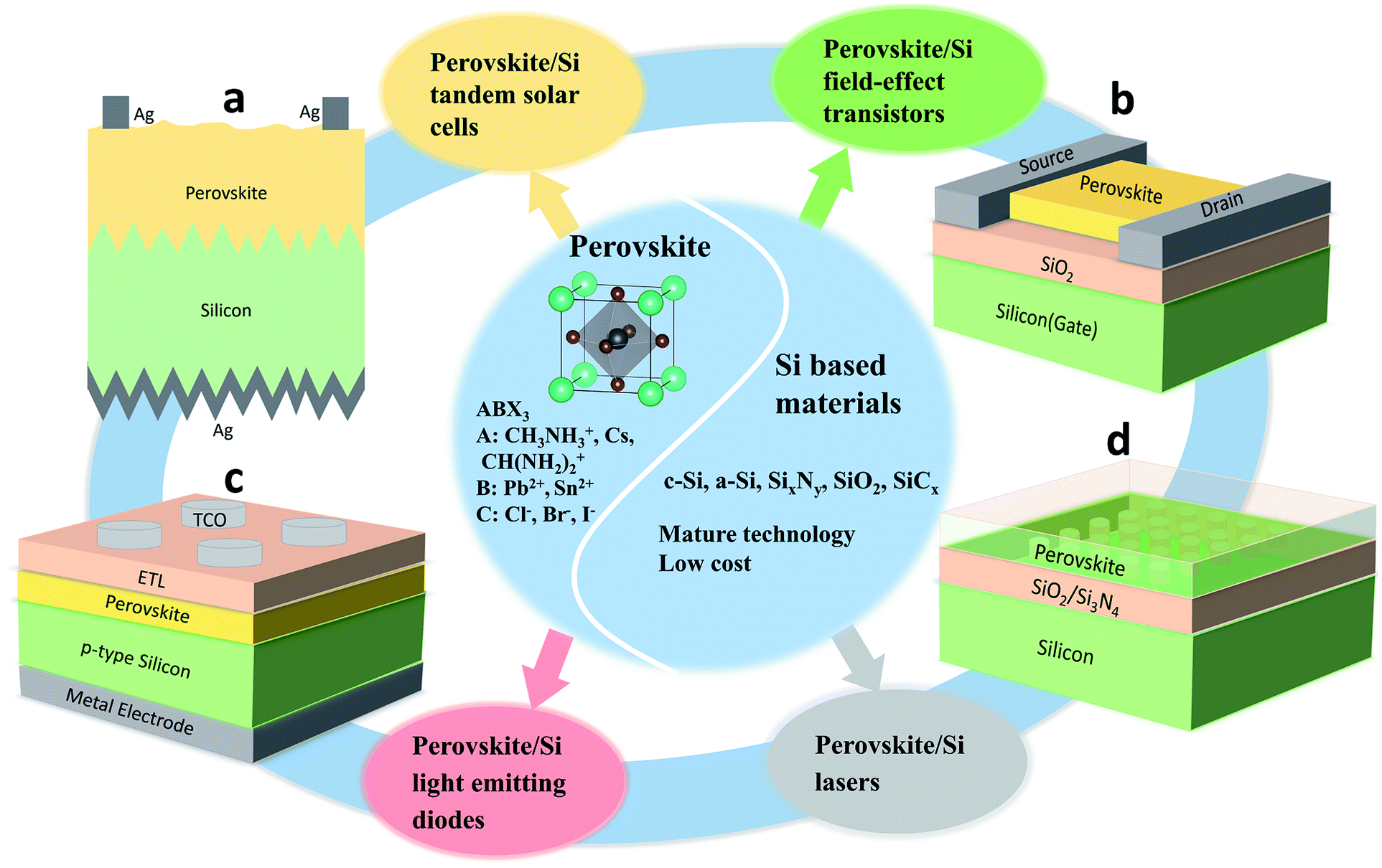 | ||
| Fig. 1 Schematic illustration of Si-based perovskite optoelectronic devices include (a) perovskite/Si tandem solar cells, (b) perovskite/Si field-effect transistor based photodetector, (c) perovskite/Si light emitting diodes and (d) Si-based perovskite lasers. | ||
Fig. 1b shows the schematic illustration of perovskite/Si field-effect transistor-based photodetectors. SiO2 are not only used as dielectric layers to passivate interface in perovskite/Si tandem, but also work as dielectrics to form a SiO2/Si capacitor in such perovskite/Si photodetectors. The band bending at the Si/SiO2 interface creates an electric field that effectively separates the optically generated electron–hole pairs in Si. In order to improve the responsivity, low-dimensional perovskites i.e. nanoplates, nanorods, nanowires and quantum dots were combined with Si to fabricate photodetectors with unique structures and photoelectric properties. Fig. 1c shows an example of a light emitting diode based on a perovskite emission layer deposited on top of a p-type silicon substrate that serves to inject holes into the perovskite. Using a structure like that, Liu et al. reported Si-based all inorganic perovskite LEDs with emission wavelengths of 515 nm and 681 nm.25 Furthermore, Xu et al. used a similar design to fabricate Si-based MAPbI3 LEDs with near-infrared (787 nm) emission.26
Fig. 1d shows the schematic illustration of an optically pumped perovskite/Si laser as reported e.g. in ref. 27. The design shown in Fig. 1d is based on the deposition of a perovskite layer on top of a periodically patterned Si wafer that was covered with SixNy or SiO2. The purpose of the patterning as discussed in ref. 28 is to reduce the lasing threshold and the emission linewidth by reducing the roughness and providing better light confinement.
2 Perovskite/Si tandem solar cells
The efficiency of single junction (SJ) solar cells illuminated with unconcentrated sunlight is limited to the fundamental SQ limit of 31–33%.8 The exact value of the SQ limit depends on the spectrum used with many recent publications using the AM1.5G spectrum that is specified in the standard testing conditions for terrestrial solar cells and leads to ≈33% (see Fig. 2a). However, the original paper used a 6000 K black body spectrum which then leads to ≈31%. As shown in Fig. 2a, the maximum efficiency is reached or nearly reached for a range of band gaps around 1.1–1.45 eV (ref. 29 and 30) which includes most technologically important semiconductors for photovoltaics such as crystalline Si (record efficiency 26.7%),29,31 Cu(In,Ga)Se2 (record efficiency 23.35%),29,32 many organic solar cell blends (record efficiency 18.2%),33,34 GaAs (record efficiency 29.1%),29,35 CdTe (record efficiency 22.1%).29,36 Only lead halide perovskites (record efficiency 25.5%),29,38 a-Si![[thin space (1/6-em)]](https://www.rsc.org/images/entities/char_2009.gif) :H (record efficiency 10.2%)29,39 and most dye-sensitized solar cells29,34,37 have band gaps that are slightly too high to be in the optimal region. While lead-halide perovskites can span a fairly wide range of band gaps, the compositions leading to the highest solar cell efficiencies can be found in the tight range between 1.5 and 1.65 eV.40
:H (record efficiency 10.2%)29,39 and most dye-sensitized solar cells29,34,37 have band gaps that are slightly too high to be in the optimal region. While lead-halide perovskites can span a fairly wide range of band gaps, the compositions leading to the highest solar cell efficiencies can be found in the tight range between 1.5 and 1.65 eV.40
 | ||
| Fig. 2 (a) Thermodynamic limit of photovoltaic conversion efficiency for single junction solar cells as a function of band gap (Shockley–Queisser limit) compared to best practically achieved efficiencies for different photovoltaic technologies.30–39 (b) Thermodynamic limit of photovoltaic conversion efficiency for tandem solar cells as a function of the two band gaps. Theoretically, efficiencies up to 45% are possible with tandem cells as compared to 33% for single junction solar cells. Panel (b) reproduced with permission.41 Copyright 2018, Wiley-VCH. | ||
Fig. 2b shows the thermodynamic limit of photovoltaic conversion efficiency for tandem solar cells as a function of the two band gaps. The thermodynamic efficiency limit for tandem solar cells is around 45% (ref. 41) and practical efficiencies may substantially exceed 30% (ref. 42 and 43) in the future. Combining the band gaps around Eg ≈ 1.1 eV of silicon with band gaps in the range of Eg ≈ 1.75 eV would then lead to the highest efficiencies in theory. Recently, the certified conversion efficiency of single junction perovskite solar cell has reached 25.5% (ref. 29 and 38) (Fig. 3, black line, data from National Renewable Energy Laboratory (NREL)) while the best efficiencies that have been published in scientific journals are currently 25.4%44 and 25.6%.45 However, note that the recent record efficiencies have nearly all been reached with compositions that are closer to the lower end of band gaps mentioned above (1.5 eV). While this trend towards lower band gaps makes sense from looking at Fig. 2a, it does not immediately benefit the search for higher efficiency tandem solar cells.
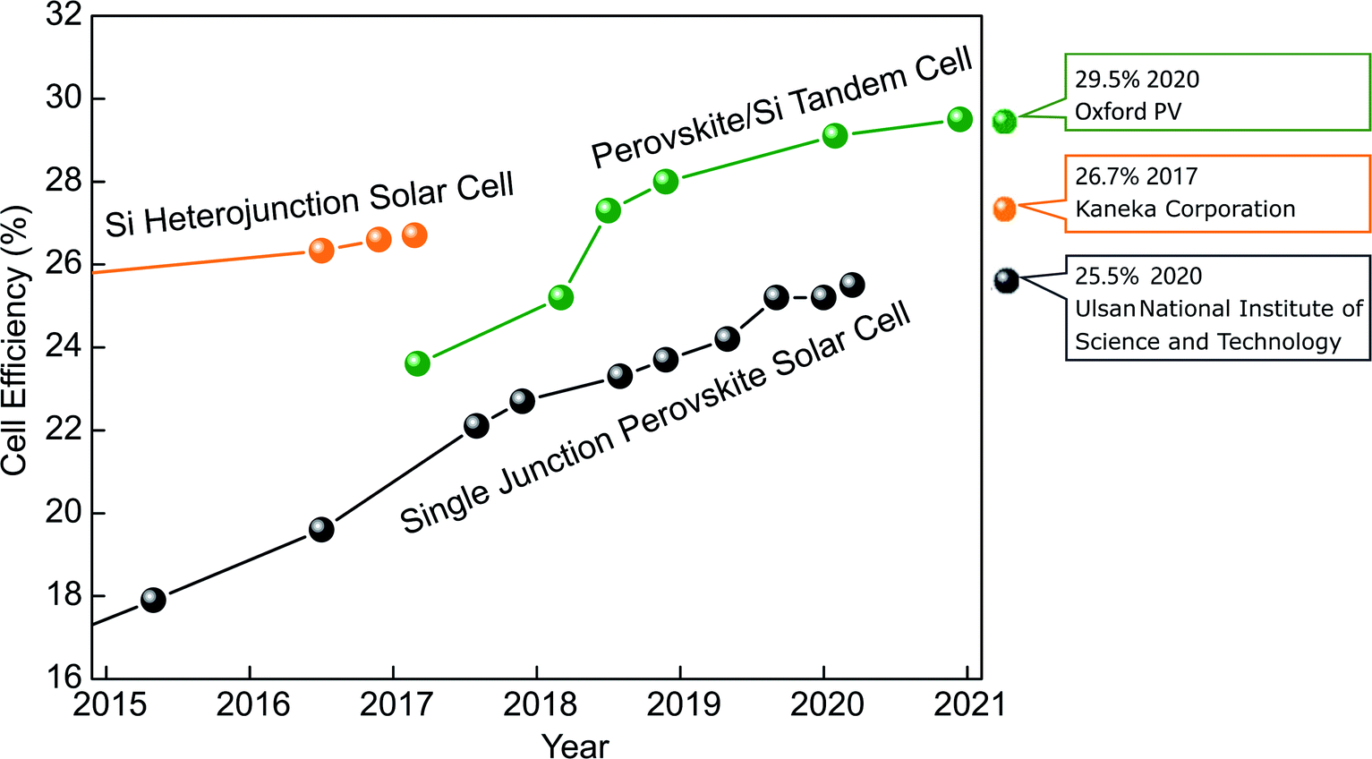 | ||
| Fig. 3 Record efficiency evolution over the last five years for silicon heterojunction solar cell (26.7% by Kaneka Corporation), single junction perovskite solar cell (25.5% by Ulsan National Institute of Science and Technology), perovskite/Si tandem cell (29.5% by Oxford PV). | ||
The energy conversion efficiency of silicon solar cells in the lab reached a record value of 26.7% in 2017 (ref. 29 and 31) (orange dotted line in Fig. 3, data from NREL) which is vital to obtain high efficiency perovskite tandem solar cell. However, these efficiencies have been reached with intermediate back contact solar cells that have both anode and cathode at the back of the cell and no metallization at the front. While this design brings obvious benefits for increasing the short-circuit current density in single junction solar cells, it is not compatible with the widely studied two-terminal tandem cells where anode and cathode are on opposite sides of the tandem cell. The best (single junction) efficiency of a double-side contacted Si solar cell compatible with two-terminal tandem designs is currently 26%.46
The goal of achieving high efficiency Si-based tandem solar cells is challenging because of the requirement of band gap matching that is necessary for two-terminal (2-T) tandem solar cells and that depends on factors such as location and climate of the photovoltaic installation, bifaciality of the system, temperature of the cell23 and the amount of optical coupling between the two subcells.47,48 This implies that depending on the exact design of the tandem cell as well as on the position on the globe or the type of installation slightly different perovskite compositions would give the optimum annual yield. Hence research has to target the optimization of perovskite solar cells with a range of band gaps between approximately 1.65 to 1.75 eV. Substantial research efforts have recently been directed towards exploring the possibilities to make efficient perovskite–Si tandem solar cells leading to an efficiency (under standard testing conditions and monofacial illumination) exceeding 29%.49–52 The efficiency of perovskite/Si tandem solar cells (green dotted line in Fig. 3, data from NREL) is therefore already substantially higher than the efficiency of single junction solar cells made from either perovskite or silicon absorber layers.
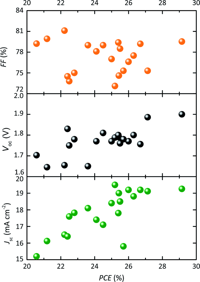
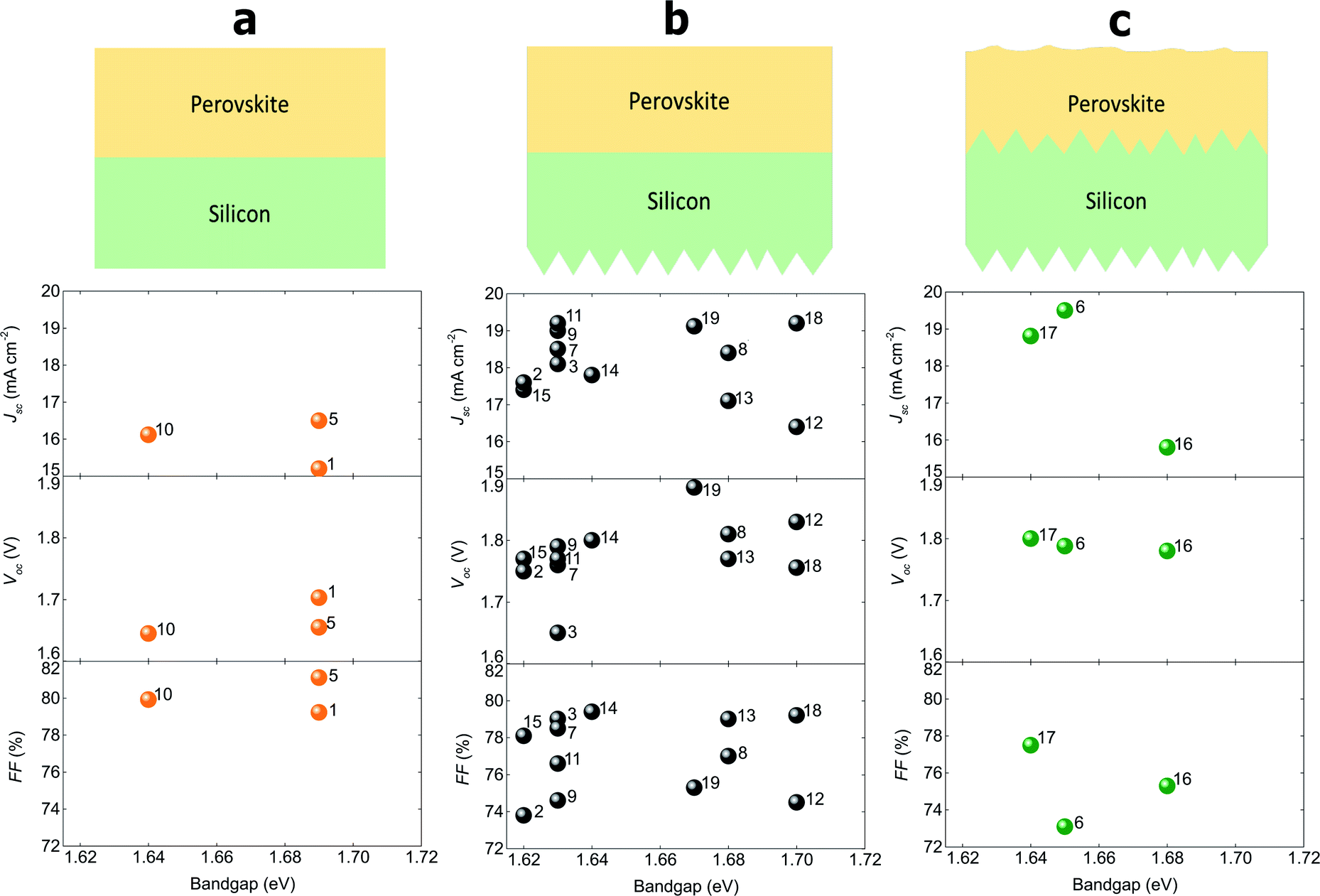
Fig. 4 plots the tandem solar cell parameters (short-circuit current density (Jsc), open-circuit voltage (Voc) and fill factor (FF)) as a function of power conversion efficiency (PCE) for those cells listed in Table 1. It is clear that the increased PCE is directly caused by the enhanced Voc and Jsc. In Fig. 4, the highest PCE for perovskite/Si tandem solar cells is 29.15%, together with 1.90 V Voc, 79.4% FF and Jsc of 19.23 mA cm−2 (ref. 53) (see line 20 in Table 1). In order to further improve the performance, both the top cell absorption and bottom silicon cell technology are important choices in the design of perovskite/Si tandem solar cell. In this section, we focus on the architecture of optimizing the current matching between the top cell and the bottom cell. We summarize various approaches to enhance absorption and reduce the optical loss between Si sub cell and the perovskite cell.
 | ||
| Fig. 4 Summary of J–V parameters from Table 1. Jsc, Voc and FF as a function of PCE, respectively. | ||
| Number | Si bottom cell | Perovskite top cell | Band gap (eV) | J sc (mA cm−2) | V oc (V) | FF (%) | PCE (%) | Area (cm2) | Year/ref. |
|---|---|---|---|---|---|---|---|---|---|
| a —, not reported; SHJ is silicon heterojunction; MA is CH3NH3+; FA is CH(NH2)2+. | |||||||||
| 1 | Flat c-Si | MA0.37FA0.48Cs0.15PbI2.01Br0.99 | 1.69 | 15.2 | 1.703 | 79.22 | 20.57 | 0.03 | 2017 (ref. 54) |
| 2 | c-Si rear texture | Cs0.07Rb0.03FA0.765MA0.135PbI2.55Br0.45 | 1.62 | 17.6 | 1.75 | 73.8 | 22.5 | 1 | 2017 (ref. 55) |
| 3 | SHJ rear texture | Cs0.17FA0.83Pb(Br0.17I0.83)3 | 1.63 | 18.1 | 1.65 | 79 | 23.6 | 1 | 2017 (ref. 56) |
| 4 | Flat SHJ | FA0.96MA0.24Cs0.1Pb1.15I3.6Br0.48 | — | 17.82 | 1.78 | 75 | 22.8 | 0.13 | 2018 (ref. 57) |
| 5 | Flat SHJ | FA0.5MA0.38Cs0.12PbI2.04Br0.96 | 1.69 | 16.5 | 1.655 | 81.1 | 22.22 | 0.06 | 2018 (ref. 58) |
| 6 | SHJ double side texture | CsxFA1−xPb(I,Br)3 | 1.65 | 19.5 | 1.788 | 73.1 | 25.2 | 1.42 | 2018 (ref. 43) |
| 7 | SHJ rear texture | Cs0.05(MA0.17FA0.83)Pb1.1(I0.83Br0.17)3 | 1.63 | 18.5 | 1.76 | 78.5 | 25.5 | 0.81 | 2018 (ref. 42) |
| 8 | SHJ rear texture | FA0.75Cs0.25Pb(I0.8Br0.2)3 | 1.68 | 18.4 | 1.77 | 77 | 25 | 1 | 2018 (ref. 59) |
| 9 | SHJ rear texture | Cs0.05(FA0.83MA0.17)0.95Pb(I0.82Br0.18)3 | 1.63 | 19.0 | 1.79 | 74.6 | 25.43 | 1 | 2019 (ref. 60) |
| 10 | Flat SHJ | (FAPbI3)0.8(MAPbBr3)0.2 | 1.64 | 16.12 | 1.645 | 79.92 | 21.19 | 0.135 | 2019 (ref. 61) |
| 11 | SHJ rear texture | Cs0.05(MA0.83FA0.17)0.95Pb(I0.83Br0.17)3 | 1.63 | 19.2 | 1.77 | 76.6 | 26.0 | 0.77 | 2019 (ref. 62) |
| 12 | SHJ rear texture | Cs0.15(MA0.83FA0.17)0.85Pb(I0.7Br0.3)3 | 1.70 | 16.4 | 1.83 | 74.5 | 22.4 | ||
| 13 | SHJ rear texture | Cs0.15(MA0.83FA0.17)0.85Pb(I0.75Br0.25)3 | 1.68 | 17.1 | 1.81 | 79.0 | 24.5 | ||
| 14 | SHJ rear texture | Cs0.15(MA0.83FA0.17)0.85Pb(I0.8Br0.2)3 | 1.64 | 17.8 | 1.80 | 79.4 | 25.4 | 0.4425 | 2019 (ref. 63) |
| 15 | SHJ rear texture | Cs0.15(MA0.83FA0.17)0.85Pb(I0.85Br0.15)3 | 1.62 | 17.4 | 1.77 | 78.1 | 24.1 | ||
| 16 | c-Si double side texture | Cs0.05MA0.15FA0.8PbI2.25Br0.75 | 1.68 | 15.8 | 1.78 | 75.3 | 25.7 | 0.83 | 2020 (ref. 64) |
| 17 | SHJ double side texture | Cs0.06FA0.78MA0.16Pb(Br0.17I0.83)3 | 1.64 | 18.81 | 1.8 | 77.5 | 26.3 | 1.43 | 2020 (ref. 65) |
| 18 | c-Si rear texture | FA0.65MA0.2Cs0.15Pb(I0.8Br0.2)3 | 1.7 | 19.2 | 1.756 | 79.2 | 26.7 | 0.188 | 2020 (ref. 66) |
| 19 | SHJ rear texture | Cs0.25FA0.75Pb(I0.85Br0.15)3 | 1.67 | 19.12 | 1.886 | 75.3 | 27.13 | 1 | 2020 (ref. 28) |
| 20 | c-Si rear texture | Cs0.05(MA0.23FA0.77)0.95Pb1.1(I0.77Br0.23)3 | 1.69 | 19.26 | 1.90 | 79.52 | 29.15 | 1.064 | 2020 (ref. 53) |
2.1 Wide band gap perovskite to top solar cell
In tandem solar cells, good current matching between the top cell and the bottom cell is the key condition for achieving a higher efficiency stacked cell than a single junction cell. The crystalline Si has a band gap of 1.12 eV, in order to current-match both junctions, a top cell material with a band gap of 1.73 eV is required under standard test conditions (AM1.5G spectrum, 1000 W m−2 25 °C).8,67–69 The band gap of typical single-junction perovskite devices is usually lower than 1.73 eV.70–73 To achieve the highest efficiencies, the current approach is to go for double or triple cation materials with a double anion (i.e. mixture of I and Br). Relative to the prototypical MAPbI3, formamidinium (FA) reduces the band gap, while Cs as a cation and Br as a partial replacement for I as an anion increase the band gap. A typical composition that gives suitable band gaps is e.g. the double cation composition FA0.83Cs0.17Pb(I0.6Br0.4)3 with 1.74 eV band gap. A four-terminal tandem cell with over 25% efficient was achieved by combining FA0.83Cs0.17Pb(I0.6Br0.4)3 cells with a 19% efficient silicon cell.74 So far the highest published efficiencies in 2-T tandem cells were achieved with a triple-cation perovskite with the composition FA0.5MA0.38Cs0.12PbI2.04Br0.96 with 1.69 eV band gap.53 In their work, a 2-T tandem device based on a silicon-heterojunction bottom cell showed over 29% efficiency with the efficiency increase relative to earlier attempts being largely due to the application of novel self-assembled monolayers (SAMs) as ultra thin hole transport layers (see Fig. 5a and line 20 in Table 1). These SAMs allowed higher fill factors due to the reduction in resistive losses and improved open circuit voltages due to better energy level alignment. At the same time, some research has focused on cation components of the 2D additives. Kim et al. developed a 2D–3D mixed wide band gap perovskite by using a mixture of thiocyanate with the more-conventional choice, iodine. The prepared monolithic perovskite–silicon tandem solar cell obtains an efficiency of 26.7% and excellent stability66 (see line 18 in Table 1). The device retained 20.7% PCE after 1000 hours of continuous illumination.66 In 2020, Xu et al. reported a 2-T monolithic Si/perovskite tandems solar cell with 27% PCE.75 Triple-halide alloys (chlorine, bromine, iodine) were used to tune the band gap of perovskite top cells. The semi-transparent top cells exhibit good stability for the standards of perovskite photovoltaics. After 1000 hours operation at maximum power point, the PCE has degraded by less than 4%. The reported results make clear that ion engineering offers an effective approach to achieve high performance tandems solar cell.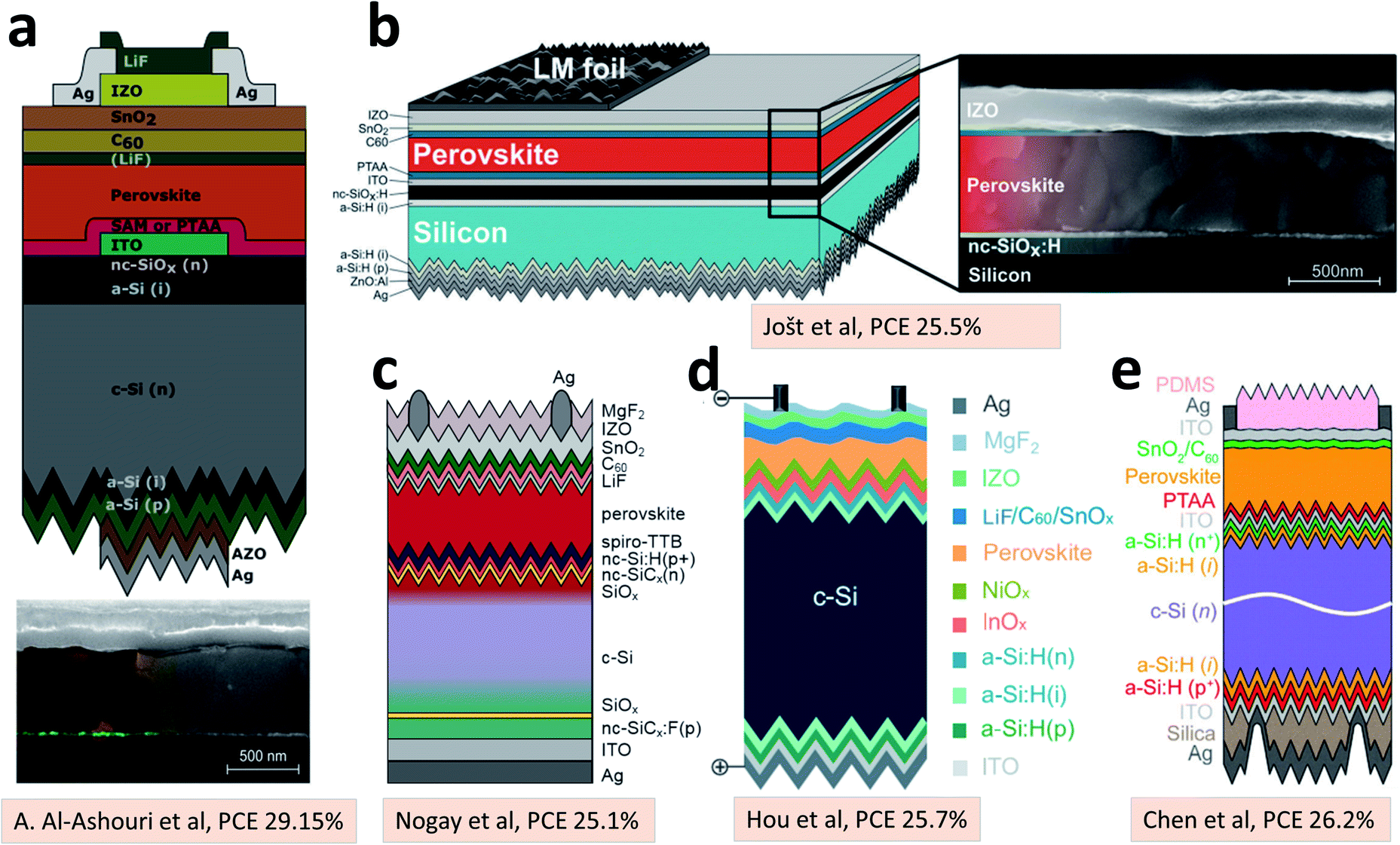 | ||
| Fig. 5 (a) Schematics stack of perovskite/Si tandem solar cell with novel self-assembled monolayers as hole transport layers and SEM image of device,53 reproduced with permission. Copyright 2020, American Association for the Advancement of Science. (b) Schematics illustration of perovskite/rear texture silicon tandem solar cell, SEM cross section image of the top cell,42 reproduced with permission. Copyright 2018, Royal Society of Chemistry. (c) Schematic of the perovskite/front texture p-type c-Si tandem solar cell,78 reproduced with permission. Copyright 2019, American Chemical Society. (d) Schematic of perovskite-textured silicon tandem architecture,64 reproduced with permission. Copyright 2020, Science. (e) Schematic view of a planarized perovskite/silicon tandem solar cell with front and rear texture,79 reproduced with permission. Copyright 2020, Elsevier. | ||
2.2 Optimization of Si-based bottom cells
At the interface between the perovskite top cell and the Si bottom cell, cell design requires a tunnel contact for electrical functionality. From an optical point of view, at this interface substantial refractive index differences occur. Silicon has substantially higher refractive indices (3.5 to 4 in the relevant wavelength range) than either the perovskite absorber or the typically used metal oxide or organic contact and transport layers. Hence, the interface between the two cells might cause significant reflection losses. In order to reduce reflection, reduce parasitic absorption, and enhance light trapping in the cell, light management is essential to improve the photocurrent absorption of silicon bottom cells. The common light management methods include the introduction of optical interlayers and textured interfaces into the device. The first monolithic perovskite/silicon tandem was made with a diffused silicon p–n junction, a tunnel junction made of n++ hydrogenated amorphous silicon (a-Si:H), TiO2 electron transport layer, methylammonium lead iodide absorber, and Spiro-OMeTAD hole transport layer.76 The PCE was only 13.7% due to low matched current density which was limited by excessive parasitic absorption of light in the hole transport layer. It is difficult to texture the contact surface with the perovskite solar cell, and the light trapping effect can only be achieved on the back surface. In order to solve this problem, Bush et al. adopted the local back contact technology that gradually entered the mainstream on crystalline silicon and use silicon nanoparticles to achieve the isolation of back silver and ITO56 (see line 3 in Table 1). The reflector comprising a silicon nanoparticle (Si NP)/silver stack show an over 99% rear internal reflectance. 300 nm thick Si NP was deposited on textured ITO film between the wafer and metal reflector to increase the rear internal reflectance by reducing the light that reaches the loss metal layer. The tandem device obtained 23.6% efficiency with no hysteresis, the stable maximum power was maintained for more than half an hour under illumination. SixNy is also used on a textured surface to balance low broadband reflection and absorption losses. It is reported that Al2O3/SixNy and SixNy films were used to passivate the front and rear surface of c-Si, respectively.55 On the front side, a specially tuned SixNy film is used to better match the refractive index of the c-Si wafer and suppress the reflection loss of the bottom cell. On the rear side of the textured c-Si cell, low refractive index SixNy is added to enhance the light trapping capability. As a result, after 1200 seconds illumination, the device achieved a PCE of 22.5% at steady state (see line 2 in Table 1). Besides, 110 nm thick nanocrystalline silicon oxide (nc-SiOx:H) with a refractive index of 2.6 was used as optical interlayer between both subcells to reduce infrared reflection losses.43 The incorporation of nc-SiOx:H interlayer in tandem cells cause a significantly increased of bottom cell current density. After optimization, the short circuit current density exceeds 19 mA cm−2 and the stabilized certified efficiency reached 25.2% (see line 6 in Table 1). In addition to Si NP, SixNy and nc-SiOx:H, wide band gap SiC were reported in solar cells to ensure high optical transparency and enable good passivation.77
In recent years, textured silicon wafers were also utilized for light management and integrating perovskite onto textured silicon which provide effective approach to 30% PCE tandem solar cells. Jošt et al. combined experimental works with optical simulations to analyze the tandems with texture at different interfaces.42 Silicon with a planar front side and textured back side was utilized as bottom cell as shown in Fig. 5b. As a result, a PCE of 25.5% was achieved for the 2-T triple cation perovskite Cs0.05(MA0.17FA0.83)Pb1.1(I0.83Br0.17)3/Si tandem solar cell (see line 7 in Table 1). The optical simulation results show the performance of front-side textured devices is significantly better than front-side planar device. The validated model result indicates the PCE potential of a best performing double-side textured device will be 32.5% for a perovskite with 1.66 eV bandgap. At the same time, p-type c-Si wafer with front texture used as bottom solar cell was reported by Nogay et al.78 In these perovskite tandem solar cells based on p-type c-Si, p-type SiCx used on the rear side to form the hole contact and n-type SiCx was used on the on front side to provide electron selectivity. In order to obtain low interface recombination, the p-type c-Si wafer is capped on both sides by an approximately 1.2 nm thick SiO2 layer. The structure of the device was shown in Fig. 5c. As a result, perovskite/p-type c-Si tandem solar cell demonstrated a steady-state power conversion efficiency of 25.1%. Fabricating tandem solar cells on double-side textured c-Si cells is a promising method to achieve high PCE, by exploiting the increased infrared absorption by light trapping and reduced front surface reflection. For the first time a double-side textured silicon bottom cell with a 25.2% certified PCE was reported by Sahli et al.43 The perovskite top cell was processed directly on the textured bottom cell. However, depositing perovskite layer on textured silicon with a typical pyramid height of several μm is still a huge challenge.
An alternative is the use of much smaller pyramids that are completely covered by the perovskite solar cell which then has to have absorber layer thicknesses of around 1 μm. One of the first successful implementations of this approach was presented by Hou et al.64 and is shown in Fig. 5d. A power conversion efficiency of 25.7% was certified by combining solution-processed micrometer-thick perovskite top cells with fully textured silicon heterojunction bottom cells (see line 16 in Table 1). The devices present stable performance after 400 hours at 85 °C. Another double-side textured tandem device was introduced by the group of Jinsong Huang (see Chen et al. in Fig. 5e).79 Silicon wafers was textured with pyramids less than 1 μm in height in potassium–hydroxide-based solutions. These pyramids are rough enough to scatter light, but smooth enough to solution process a perovskite layer. Here, a dense perovskite absorber film on textured silicon is fabricated by N2-assisted blade coating at a speed of 1.5 m min−1, followed by thermal annealing for perovskite crystallization. Textured light-scattering layer on the top of the tandem cell is employed to reduce the reflectance of front-surface. As a result, perovskite/double-side textured silicon tandem cell achieved a PCE of 26.2%. Fig. 6 presents schematic illustrations of perovskite/silicon tandem solar cells by implementing textures at different interfaces and the J–V parameters from Table 1. The simplest device design without any textured interfaces is shown in Fig. 6a. Fig. 6b and c represent perovskite/silicon tandem solar cells utilizing a rear-side textured Si subcell and double-side textured Si subcell, respectively. The back-side texture enhances photocurrent generation in the near infrared wavelength region. The front-side textured reduces reflection and enables enhanced light trapping by backscattering the upward propagating light.64J–V parameters in Fig. 6 show textured light management enables significant gains in photocurrents. Optical interlayers and textured interfaces are effective methods to reduce the optical losses in tandem device.
 | ||
| Fig. 6 Schematic illustration of perovskite/silicon tandem solar cell with different bottom cell and summary of J–V parameters. The numbers in the figure are consistent with those in Table 1. (a) Perovskite/silicon tandem solar cell with flat Si subcell. (b) Perovskite/silicon tandem solar cell with rear texture Si subcell. (c) Perovskite/silicon tandem solar cell with a double textured Si subcell. | ||
3 Si-based perovskite photodetectors
Photodetectors have important applications in military, aerospace, communications, and biological imaging.80–83 A photodetector is a device for detecting and measuring a photon flux via the photoelectric effect, which generally manifests as a photocurrent. In a photodetector, the semiconductor material is essential for absorbing incident photons and generating electron–hole pairs under photoexcitation. Then the electrons and holes are separated by a built-in or applied electric field to produce an electric current. One of the most common photodetector types is a photoconductor with a metal–semiconductor–metal architecture forming the source and drain electrodes. Photo field-effect transistors (photo-FET) based photodetectors are similar to photoconductors with a third contact gate electrode. The most important parameters to evaluate the performance of photodetectors include the response time (rise time and decay time), the responsivity (R, A W−1), the detectivity (D*, Jones), the external quantum efficiency (EQE, %), the photoconductive gain (G) and the photocurrent/dark-current ratio. Inorganic semiconductors such as Si and GaN are widely used for photodetectors especially for UV-light metal–semiconductor–metal architecture forming the source and drain electrodes. However, the fabrication processes are complex and expensive, and photodetectors with high driving voltage are an obstacle for some applications. In the past few years, solution processable materials such as halide perovskite have shown the potential for preparing photodetectors with a simple process, low cost and high responsivity. The prepared photodetectors based on polycrystalline perovskite films typically exhibit performance degradation which can be avoided e.g. by using low-dimensional halide perovskites with high crystallinity.84–87 In order to further increase the responsivity, low-dimensional perovskites have been combined with other low-dimensional materials such as graphene, tungsten disulfide and molybdenum disulfide to fabricate photodetectors with unique structures and photoelectric properties. Table 2 summarizes the performance parameters of low-dimensional perovskite photodetectors based on SiO2/Si. Fig. 7a shows the responsivity and response time of various perovskite photodetector (including nanosheets (NSs)/nanoplates, nanowires (NWs)/nanorods (NRs), quantum dots (QDs)/nanocrystals (NCs) and microparticles). A structure–responsivity relationship of low dimensional perovskite photodetector was present. Fig. 7b plots the detectivity versus light source wavelength for reported low dimensional perovskite photodetectors. The wavelength of light sources ranges from 400 nm to 650 nm. The highest values of responsivities and detectivities are 8.2 × 10⁸ A W−1 and 2.4 × 10¹⁶ Jones, respectively (Fig. 7a and b), which were achieved by CsPbBr3−xIx nanocrystal photodetectors. In this section, we present the recent developments of Si-based low dimensional halide perovskite photodetectors.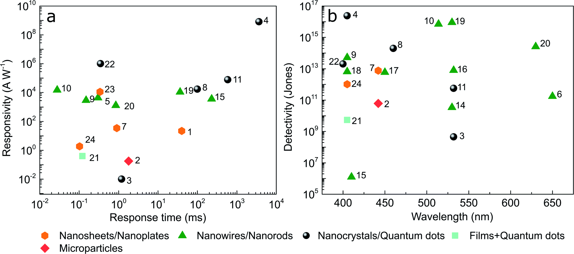 | ||
| Fig. 7 (a) Various perovskite photodetector technologies plotted against their corresponding responsivity and time response. (b) Detectivity of Low dimensional perovskite photodetector as a function of light source wavelength. The numbers are corresponding to those in Table 2. | ||
3.1 Perovskite nanosheets/Si photodetectors
2D perovskites have a unique planar geometry, which is advantageous for fabricating thin-film devices. A rich engineering of 2D perovskite has been demonstrated by many different methods, including micromechanical exfoliation,108 chemical vapor deposition109–111 and one-step solution self-assembly.112 The uncontrolled precipitation of the perovskite will produce large morphological variations, which would be the major barriers for practical applications. Liu et al.84 reported 2D CH3NH3PbX3 perovskite as thin as a single unit cell by using a combined solution process and vapor-phase conversion method (see Fig. 8a). The 2D CH3NH3PbI3 nanosheets with different thickness all show high quantum efficiency in terms of photoluminescence (PL) yield but different PL peak positions. Liu et al.84 prepared phototransistors based on CH3NH3PbI3 nanosheets on SiO2/Si substrate (see Fig. 8b). In the device fabrication process, a patterned Si3N4 shadow mask was used to prevent doping while Si is used as gate electrode, and Au was used as source and drain electrode. As a result, the 2D CH3NH3PbI3 nanosheets photodetector showing responsivity of 22 A W−1 (see Fig. 8c), the rise time is shorter than 20 milliseconds (ms) and the decay time is shorter than 40 ms (see line 1 in Table 2). Parveen et al.107 also achieved highly tuneable thickness and optical properties of the organic–inorganic halide perovskite by using a short-term solvothermal reaction method and controlling growth temperature (see Fig. 8d). The fabricated 2D perovskite nanosheets photodetector device based on Si/SiO2 substrate shows good stability, fast response time (rise time 24 μs/fall time 103 μs) and a responsivity of ≈1.93 A W−1 (see Fig. 8e, f and line 24 in Table 2). Pan and co-authors106 developed a fully vapor-phase method to grow highly crystalline and thickness-tuneable (CH3NH3)n+1PbnI3n+1 layers on top of WS2 monolayer (see Fig. 8g). The schematic image of perovskite/WS2 heterostructures field-effect transistors is shown in Fig. 8h. The (CH3NH3)n+1PbnI3n+1/WS2 heterostructure photodetectors exhibit a photoresponsivity of 1.1 × 10⁴ A W−1 (see Fig. 8i, line 23 in Table 2). Gao et al.113 demonstrated the synthesis of 2D halide perovskite lateral heterostructures via a solution-phase sequential growth method. Concentric square/rectangular 2D lateral heterostructures can be formed directly on the SiO2/Si substrate. The obtained epitaxial heterostructures, multi-heterostructures and superlattices present highly stable and tuneable electronic properties. These findings open up the possibility of further exploring 2D halide perovskite lateral heterostructures' optoelectronic properties and their applications in optoelectronic devices and integrated circuits.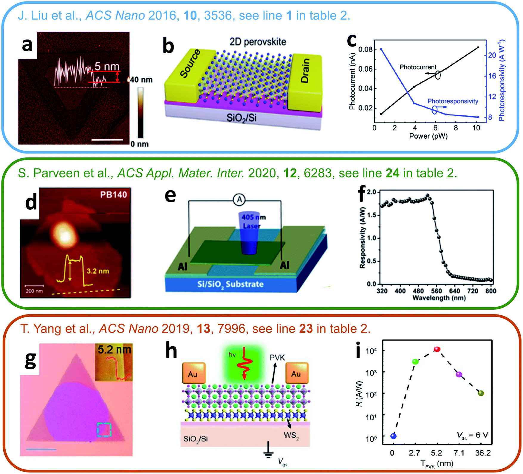 | ||
| Fig. 8 Perovskite nanosheets/Si photodetectors structures and performance. (a, d, g) AFM images and line scan profiles of perovskite nanosheets, (a) CH3NH3PbI3 nanosheet, (d) CH3NH3PbBrI2 nanosheet, (g) (CH3NH3)n+1PbnI3n+1 nanosheet. (b, e, h) Schematic images of photodetectors based on 2D perovskite nanosheets. (c, f, i) Photodetector responsivity (a, b, c) Reproduced with permission84 (see line 1 in Table 2). Copyright 2016, American Chemical Society. (d, e, f) Reproduced with permission107 (see line 24 in Table 2). Copyright 2020, American Chemical Society. (g, h, i) Reproduced with permission106 (see line 23 in Table 2). Copyright 2019, American Chemical Society. | ||
| Number | Device structure | Perovskite Size (nm) width/length | Light source (nm) | Bias (V) | Rise/decay time | R (A W−1) | D* (Jones) | Year/ref. |
|---|---|---|---|---|---|---|---|---|
| a Notes: — not reported, R is responsivity, D* is detectivity, NW is nanowire, NR is nanorod, NP is nanoparticle, NC is nanocrystal, MP is microparticle, QD is quantum dot, ms is millisecond. | ||||||||
| 1 | Si/SiO2/CH3NH3PbI3 NS/Au | 5 | 405 | 1 | 20/40 ms | 22 | — | 2016 (ref. 84) |
| 2 | Si/SiO2/CsPbBr3 MP/Au | — | 442 | 10 | 1.8/1.0 ms | 1.8 × 10⁻¹ | 6.1 × 10¹⁰ | 2016 (ref. 88) |
| 3 | Si/SiO2/CsPbBr3 NP/Au | 60–70/— | 532 | 2 | 0.2/1.2 ms | 1.004 × 10⁻² | 4.56 × 10⁸ | 2016 (ref. 89) |
| 4 | Si/SiO2/CsPbBr3−xIx NC/Ti/Au | 10/— | 405 | 1 | 0.81/3.65 s | 8.2 × 10⁸ | 2.4 × 10¹⁶ | 2016 (ref. 90) |
| 5 | Si/SiO2/CsPbI3 NW/Au | 200–800/several mm | 405 | 3 | 0.252/0.3 ms | 4.4 × 10³ | — | 2017 (ref. 91) |
| 6 | Si/SiO2/CH3NH3PbI3 NW/Au | 400/— | 650 | — | — | 1.25 × 10⁴ | 1.73 × 10¹¹ | 2017 (ref. 92) |
| 7 | Si/SiO2/CsPbBr3 nanoplate/Au | 10 μm | 442 | 1.5 | 0.6/0.9 ms | 3.4 × 101 | 7.5 × 10¹² | 2017 (ref. 93) |
| 8 | Si/SiO2/CsPbBr3 QD/DNTT/Au | 10 nm | 460 | 10 | 50/100 ms | 1.7 × 10⁴ | 2.0 × 10¹⁴ | 2017 (ref. 94) |
| 9 | Si/SiO2/CsPbI3 NR/Au | 150/2000 | 405 | 2 | 0.05/0.15 ms | 2.92 × 10³ | 5.17 × 10¹³ | 2018 (ref. 95) |
| 10 | Si/SiO2/(BA)2(MA)n−1PbnI3n+1 NW/Au | 150–15000/400–10500 |
514 | 5 | 27.6/24.5 μs | 1.5 × 10⁴ | 7 × 10¹⁵ | 2018 (ref. 96) |
| 11 | Si/SiO2/MoS2/CsPbI3−xBrx QD/Au | — | 532 | 1 | 0.59/0.32 s | 7.7 × 10⁴ | 5.6 × 10¹¹ | 2018 (ref. 97) |
| 12 | Si/SiO2/CsPbBr3 NW arrays/Ti/Au | 12/— | 405 | 6 | 82/54 ms | — | — | 2018 (ref. 98) |
| 13 | Si/SiO2/CsPbCl3 NW arrays/Ti/Au | 9/— | 405 | 8 | 70/45 ms | — | — | |
| 14 | Si/SiO2/CsPbI3 NW/Au | 300/several mm | 530 | 1 | — | 7.45 × 10⁻¹ | 3.46 × 10¹⁰ | 2018 (ref. 99) |
| 15 | Si/SiO2/Cs3Sb2Cl9 NR/Au | 20/165 | 410 | 0.9 | 130/230 ms | 3.616 × 10³ | 1.25 × 10⁶ | 2018 (ref. 100) |
| 16 | Si/SiO2/CsPbI3 NW/Ti/Au | 150/— | 532 | 5 | — | 4.489 × 10³ | 7.9 × 10¹² | |
| 17 | Si/SiO2/CsPbBr3 NW/Ti/Au | 150/— | 450 | 5 | — | 3.306 × 10³ | 6.0 × 10¹² | 2019 (ref. 101) |
| 18 | Si/SiO2/CsPbCl3 NW/Ti/Au | 150/— | 405 | 5 | — | 1.183 × 10³ | 6.6 × 10¹² | |
| 19 | Si/SiO2/(ThMA)2(MA)n−1PbnI3n+1 NW arrays/Cr/Au | — | 530 | 5 | 36.3/31.5 μs | 1.1 × 10⁴ | 9.1 × 10¹⁵ | 2019 (ref. 102) |
| 20 | Si/SiO2/CsPbI3 NW arrays/Cr/Au | 250/— | 630 | 5 | 0.85/0.78 ms | 1.294 × 10³ | 2.6 × 10¹⁴ | 2019 (ref. 103) |
| 21 | Si/SiO2/CH3NH3PbI3−xClx film/CsPbBr3 QD/Au | 20 | 405 | 1 | 121/107 μs | 3.9 × 10⁻¹ | 5.43 × 10⁹ | 2019 (ref. 104) |
| 22 | Si/SiO2/graphene/CsPbCl3 NC/Au | 10.5 | 400 | 0.5 | 0.3/0.35 ms | 1 × 10⁶ | 2 × 10¹³ | 2019 (ref. 105) |
| 23 | Si/SiO2/WS2/(CH3NH3)n+1PbnI3n+1NS/Au | 5.2 | 520 | 6 | 0.18/0.34 ms | 1.1174 × 10⁴ | — | 2019 (ref. 106) |
| 24 | Si/SiO2/CH3NH3PbBrI2 NS/Au | 3.2 | 405 | 0 | 24/103 μs | 1.9 | 1.04 × 10¹² | 2020 (ref. 107) |
3.2 Perovskite nanowires/Si photodetectors
1D nanowire semiconductors have great potential in future electronic circuits and optical chips due to their high crystallinity,114 large surface-to-volume ratio,115 and chip level polarization sensitivity.116,117 The synthesis methods of nanowires include solution-phase118,119 and vapor-phase120,121 processes. For the vapor-phase method, SiO2/Si, mica and sapphire are usually used as growth substrate to promote perovskite NWs growth. SiO2/Si can also be used as the NWs growth channel combined with photoresist and photolithography technology to achieve directional growth of perovskite nanowires. Photodetectors based on 1D halide perovskites have been reported and made great progress with respect to responsivity and detectivity. Deng et al. obtained single-crystalline MAPbI3 NWs with smooth surface by fluid-guided antisolvent vapor-assisted crystallization method92 (see Fig. 9a). In the fabrication process of nanowires, a SiO2/Si substrate with periodically aligned SU-8 photoresist stripes served as a template for the subsequently aligned growth of perovskite NWs arrays. The schematic and the performance metrics responsivity and photoconductive gain of MAPbI3 NWs photodetector using an SiO2/Si substrate are shown in Fig. 9b. The photodetector exhibits a broad photo-response range from 370 to 780 nm and high light sensitivity with maximum spectral responsivity of approximate 1.25 × 10⁴ A W−1 (see Fig. 9c and line 6 in Table 2). Stability is one of the key challenges for the technology of perovskite device. In order to achieve stable perovskite devices, all inorganic perovskite-nanowires arrays were also utilized to fabricate photodetectors (see line 20 in Table 2).103 Chen et al. fabricated α-CsPbI3 nanowires by employing an asymmetric-wettability topographical template, and prepared photoconductor-type photodetectors on silicon103 (see Fig. 9d and e). The stable α-CsPbI3 nanowire array based photodetectors present responsivity of 1.294 × 10³ A W−1 responsivity (see Fig. 9f), 2.6 × 10¹⁴ Jones detectivity and long stability (see line 20 in Table 2). In addition to CsPbI3 nanowires, 1D all inorganic CsPbI3 nanorods-based photodetectors have also been reported by Yang et al. The single crystalline CsPbI3 nanorods with high quality were synthesized with a high yield via a solution process (see Fig. 9g and h). The inorganic perovskite-nanorods photodetector exhibited a responsivity of 2.92 × 10³ A W−1 (see Fig. 9i) and 0.9 × 10⁶ % EQE with 2 V bias voltage and 405 nm light95 (see line 9 in Table 2). More importantly, the CsPbI3-nanorod photodetectors showed high stability when kept under ambient conditions,95 which are promising to realize efficient practical application of optoelectronic devices.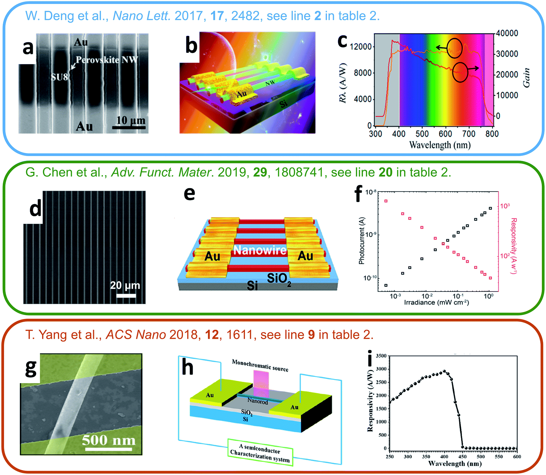 | ||
| Fig. 9 Perovskite nanowires (nanorods)/Si photodetectors structures and performance. (a, d, g) SEM images of (a) CH3NH3PbI3 nanowire arrays, (d) α-CsPbI3 nanowire arrays, and (g) a CsPbI3 nanorod. (b, e, h) Schematic illustrations of photodetectors based on 1D perovskite nanowires (nanorods). (c, f, i) Photodetector responsivity. (a, b, c) Reproduced with permission92 (see line 6 in Table 2). Copyright 2017, American Chemical Society. (d, e, f) Reproduced with permission103 (see line 20 in Table 2). Copyright 2019, Wiley-VCH. (g, h, i) Reproduced with permission95 (see line 9 in Table 2). Copyright 2018, American Chemical Society. | ||
3.3 Perovskite quantum dots/Si photodetectors
Inorganic perovskites QDs or NCs have emerged as a new class of photoelectronic materials owing to their relatively high stability ascompared to organic–inorganic perovskites, cost effectiveness,122 over 90% photoluminescence quantum yield in solution,123 tuneable emission wavelengths and absorption onsets.124 All-inorganic CsPbI3 nanocrystals NCs were first employed in photodetectors by Ramasamy et al. in 2016.125 The photodetectors fabricated from CsPbI3 NCs exhibited 24 ms rise time and 29 ms decay time. However, the photoresponsivity of photodetectors is limited by the low charge transport efficiency of the inorganic QDs layers.94 Chen et al. combined CsPbBr3 QDs with organic semiconductors (dinaphtho[2,3-b:2′,3′-f]thieno[3,2-b]thiophen (DNTT)) to fabricate heterostructure photodetectors to improve the transportation of the photo-excited charges (see Fig. 10a and b). The devices showed a photoresponsivity of ≈1.7 × 10⁴ A W−1, and a detectivity of ≈2.0 ×10¹⁴ Jones (see Fig. 10c and line 8 in Table 2). Wu et al. integrated CsPbI3−xBrx QDs with monolayer MoS2 for low-cost and high performance heterostructure photodetectors.97 The CsPbI3−xBrx QDs have a typical cubic shape with an average diameter of 15 nm (see Fig. 10d). The monolayer MoS2 used as the channel of phototransistor. Authors synthesized monolayer MoS2 by oxygen-assisted chemical vapor deposition. And then transferred it onto SiO2/Si substrate by a PMMA-assisted transfer method. In the mixed-dimensional hetero-structure photodetectors (see Fig. 10e), a favourable energy band alignment is conducive to interfacial photocarrier separation and efficient carrier injection into the MoS2 layer. The optimized mixed-dimensional heterostructure photodetectors exhibited a high photo-responsivity of 7.7 × 10⁴ A W−1, 5.6 × 10¹¹ Jones detectivity and 107% EQE (see Fig. 10f and line 11 in Table 2). Gong et al. reported a passivation process with a thiol on CsPbCl3 NCs to improve performance of photodetectors.105 The CsPbCl3 NCs have an average size of 10.5 nm (see Fig. 10g). The surface engineering can not only facilitate high efficiency charge transfer in field-effect transistors but also minimize the charge trapping and prevent degradation of the devices based on CsPbCl3 NCs. The devices (see Fig. 10h) obtained a responsivity exceeding 106 A W−1, a detectivity of 2 × 10¹³ Jones and ambient stability for more than 2400 h (see Fig. 10i and line 22 in Table 2). Yang et al. reported photodetectors based on CH3NH3PbI3−xClx layers and CsPbBr3 QDs on a SiO2/Si substrate.104 After introducing inorganic perovskite QDs into CH3NH3PbI3−xClx photodetector, the device achieved a higher gain with a lower dark current than single CH3NH3PbI3−xClx photodetector. The maximum responsivity of CH3NH3PbI3−xClx perovskite–CsPbBr3 QDs hybrid photodetector is obviously larger than that of CH3NH3PbI3−xClx perovskite photodetectors without CsPbBr3 QDs. The enhanced responsivity is attributed to the ability of the CsPbBr3 QDs to achieve efficient light absorption and carrier injection into the perovskite layer. The devices exhibited ≈121 μs rise time and ≈107 μs fall times (see line 21 in Table 2).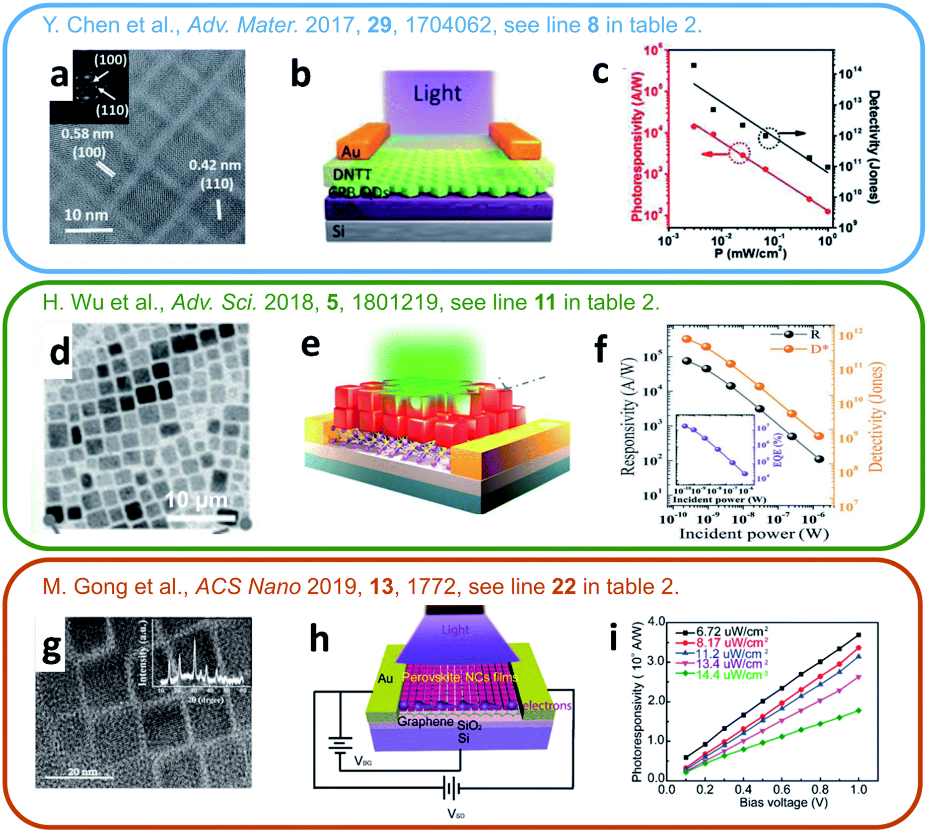 | ||
| Fig. 10 Perovskite QDs (NCs)/Si photodetectors structures and performance. (a, d, g) TEM images of perovskite QDs (nanocrystal), (a) CsPbI3−xBrx QDs, (d) CsPbCl3 NCs, (g) CsPbBr3 QDs. (b, e, h) Schematic illustrations of photodetector based on perovskite QDs (nanocrystal). (c, f, i) The device performance. (a, b, c) Reproduced with permission94 (see line 8 in Table 2). Copyright 2017, Wiley-VCH. (d, e, f) Reproduced with permission97 (see line 11 in Table 2). Copyright 2018, Wiley-VCH. (g, h, i) Reproduced with permission105 (see line 22 in Table 2). Copyright 2019, American Chemical Society. | ||
Due to the mature technology of Si-based devices, researchers have also combined silicon directly with perovskite QDs to prepare heterojunction photodetectors. The interface of the perovskite–Si heterojunction can promote the separation and transmission of photo-generated carriers, which can not only broaden the light detection range, but also increase the light response rate.126 The perovskite quantum dots are evenly distributed on the surface of the three-dimensional framework of the Si nanowire radial junction. Perovskite quantum dots on the surface of the device absorb high-energy photons, and then convert them into lower-energy photons that are absorbed in the Si-based p–n junction region to realize sensitive photodetection. The Si nanowire radial junction (with 80 nm i-layer) can respond to the visible 512 nm wavelength modulation.
After spin-coating inorganic perovskite CsPbBr3 QDs on the surface of the Si nanowire, the perovskite QDs radial junction detector can catch up the alternating stimulations up to ≈1 kHz. The Si nanowire/CsPbBr3 QDs photodetector exhibited 0.48/1.03 ms rise/fall time for UV wavelength detection. Combining the two materials results in a highly efficient silicon-based perovskite detector, which provides a new and effective way for photoelectric integration of portable multi-functional devices.
4 Si-based perovskite light emitting diodes
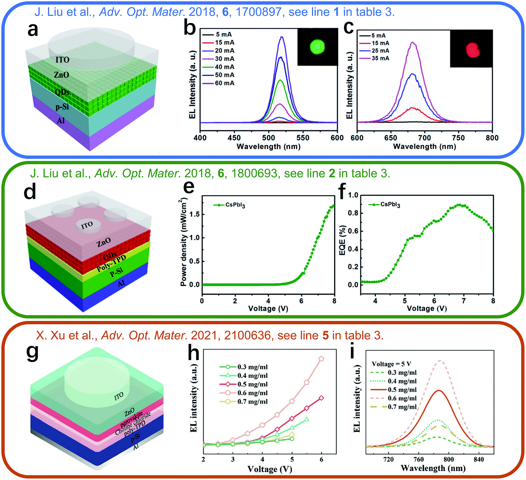
In general, LEDs consist of a transparent electrode (e.g., FTO, ITO), electron-transporting layer, emitter layer, hole-transporting layer and back electrode. The carriers are injected through the electrode and transported efficiently to the emitter layer, following by radiative recombination and generating light emission. The generated light is transmitted through the electron-transporting layer or hole-transporting layer and the transparent electrode. For a high-performance device, the choice of emitter material and the design and selection of the interfaces are critical to suppress unwanted non-radiative recombination. Perovskites with a direct band gap have the advantages of adjustable wide spectral band gap and high luminescence quantum efficiency, and have therefore important application prospects in the field of light sources. But low stability is the biggest obstacle to perovskite's commercial application. Inorganic perovskite QDs demonstrate better thermal stability and low humidity sensitivity. They are expected to be new generation of light-emitting display materials. In 2015, Protesescu et al. reported the first successful preparation of CsPbX3 (X = Cl, Br, I, and their mixtures) nanocrystals by the thermal injection method.127 In 2016, researchers have developed all-inorganic perovskite QDs (CsPbX3, X = Cl, Br, I, and their mixtures) in practical applications.128 In the past few years, researchers have improved the luminous efficiency and stability of inorganic perovskite QDs LEDs through surface modification of QDs, interface modification and carrier transport layer optimization. All inorganic hole transport materials (NiO2, MoO3, CuSCN) and electron transport materials (ZnO, TiO2) were utilized in devices to overcome the emission efficiency and operational stability.8,41 Impressive external quantum efficiencies (EQEs) up to 21.6% in the near-infrared (NIR) region,129 21.3% in the red region,130 22% in green region and 12.3% in the blue region131 have been achieved.Several groups combined perovskite emission layers with Si-based substrates to fabricate LEDs as listed in Table 3. Liu et al. demonstrated inorganic CsPbX3 QDs/p-type Si heterojunction LEDs by using p-type crystalline Si as hole transport layer (Fig. 11a).25 The perovskite/Si heterojunction LEDs show strong green and red light emission (Fig. 11b and c). The full width at half maximum of emission peak is very narrow, nearly 22 nm and 30 nm for the green and red emission, respectively. The authors optimized the energy band alignment to improve the performance of Si-based perovskite LEDs.132Fig. 11d shows the schematic and energy band diagrams of device. After optimizing the energy level, the hole injection barrier is reduced. The Si/CsPbI3 QDs LEDs obtained 1.68 mW cm−2 output power density and 0.91% EQE (Fig. 11e and f).
| Number | Perovskite | Device structure | EL (nm) | FWHM (nm) | EQE (%) | Driving mode | Max lumin. (cd m−2) | Year/ref. |
|---|---|---|---|---|---|---|---|---|
| a Notes: — not reported, QDs is quantum dots, EL is electroluminescence, FWHM is full width at half maximum, DC is direct current, AC is alternating current. | ||||||||
| 1 | CsPbBr3 QDs | Al/p-Si/perovskite/ZnO/ITO | 512 | 22 | — | DC | — | 2018 (ref. 25) |
| CsPbI3 QDs | Al/p-Si/perovskite/ZnO/ITO | 685 | 30 | — | DC, AC | — | ||
| 2 | CsPbI3 QDs | Al/p-Si/poly-TPD/perovskite/ZnO/ITO | 690 | 30 | 0.91 | DC | 665 | 2018 (ref. 132) |
| CsPbBr3 QDs | Al/p-Si/Au/poly-TPD/perovskite/ZnO/ITO | 513 | 22 | — | DC | 403 | ||
| 3 | CsPbI3 QDs | Al/p-Si/poly-TPD/perovskite/ZnO/ITO | 690 | 30 | — | AC | 850 | 2018 (ref. 133) |
| 4 | CsPbBr3 QDs | Si/SiO2/perovskite/Au | 555.8 | 12.2 | — | AC | — | 2018 (ref. 134) |
| 5 | MAPbI3 films | Al/p-Si/poly-TPD/ChCl/perovskite/ZnO/ITO | 785 | 55 | 3.92 | DC | — | 2021 (ref. 26) |
 | ||
| Fig. 11 (a, d, g) Schematic image of inorganic perovskite QDs/Si LEDs. (b, c, e, f, h, i) Performance of LEDs. (b) Electroluminescence (EL) spectra of CsPbBr3 QDs LEDs at different injection current, inset shows emission photograph of the CsPbBr3 QDs LEDs at 60 mA. (c) EL spectra of CsPbI3 QDs LEDs at different injection current. The inset shows the emission photograph of the LEDs. (e and f) Power density and EQE as a function of voltage for CsPbI3 QDs LEDs. (h and i) EL intensity as a function of voltage and wavelength. (a–c)25 Reproduced with permission. Copyright 2018, Wiley-VCH. (d–f)132 Reproduced with permission. Copyright 2018, Wiley-VCH. (g–i)26 Reproduced with permission. Copyright 2021, Wiley-VCH. | ||
The performance of perovskite/p-Si LEDs under different driving modes was studied in ref. 133. Compared to LEDs under direct current (DC) mode, LEDs show higher EL intensity, lower power consumption and better stability when driven in alternating current (AC) mode.25,133 Recently, Xu et al. reported near-infrared (NIR) perovskite light-emitting diodes based on Si (see Fig. 11g).26 Choline chloride was used as passivation layer to improve the EL intensity of devices. The LEDs with 0.5 mg ml−1 choline chloride achieved higher EL intensity than other devices. The Si–MAPbI3 LEDs present NIR wavelength emission with 785 nm spectra peak and a full width at half maximum (FWHM) of 55 nm. The performance of perovskite LEDs based on Si is still lower than perovskite LEDs with organic transport layers. The perovskite/Si light emitting diodes are still at an early stage of development. The large leakage current, low EQE and short lifetime are the urgent problems that need to be overcome.
5 Si-based perovskite lasers
Lasers occupy important position in people's lives and have been widely used in various technical and scientific fields, such as biological imaging, manufacturing, spectroscopy and optical communications.135 Halide perovskite exhibits potential applications in laser136–147 due to high luminescence quantum yield,148 tuneable emission wavelength11 and low defect state density.18 Up to date, most of perovskite lasers are optically pumped. Nanostructures in optically pumped laser could not only provide optical feedback,149,150 but also reduce the lasing threshold as well as increase the quality factor by reducing the roughness and providing better light confinement.23 Perovskite nanostructures, such as single crystalline nanowires and nanoplates, can be used as both gain media and optical microcavities, which is particularly promising for high-quality small-sized laser sources.151–153 However, it is difficult to fabricate patterned perovskites arrays directly due to the urgent challenges of the incompatibility of perovskite with the typical lithographic process.154 In contrast, the process of preparing patterned Si-based materials through photolithography or electron beam lithography is a mature technology. Patterned perovskite could be obtained by integrating halide perovskites with Si-based pre-patterned substrate. Optical resonator is the main part of laser, which has different shape and architecture. Researchers have demonstrated optically pumped lasers based on Si using various optical feedback structures such as whispering gallery cavities (WG), photonic crystal bandedge and distributed feedback gratings.67Table 4 summarized the characteristics of Si-based perovskite lasers with different mode.| Number | Perovskite | Device structure | Lasing type | Wavelength (nm) | Threshold | Δλ (nm) | Year/ref. |
|---|---|---|---|---|---|---|---|
| a Notes: — not reported, WGM is whispering gallery mode, PhC is photonic crystal, DFB is distributed feedback, Δλ is full width at half maximum (fwhm). | |||||||
| 1 | MAPbI3 nanoplatelets | Si/perovskite | WGM | 780–790 | 40 μJ cm−2 | 0.9 | 2014 (ref. 109) |
| 2 | MAPbBr3 microsphere | Glass/SiO2 sphere/perovskite | WGM | — | 65 μJ cm−2 | — | 2014 (ref. 155) |
| 3 | CsPbX3 nanocrystals | SiO2 sphere/perovskite | WGM | 440–700 | 5 μJ cm−2 | 0.15–0.2 | 2015 (ref. 156) |
| 4 | MAPbI3 microplatelet | Si/SiO2/patterned h-BN/perovskite | WGM | 770 | 37 μJ cm−2 | 5.4 | 2016 (ref. 157) |
| 5 | MAPbBr3 microplate | Si grating/perovskite | WGM | — | 5.4 μJ cm−2 | — | 2016 (ref. 158) |
| 6 | MAPbI3 film | Si/SiO2/Si3N4/perovskite | PhC | 780 | 200 μJ cm−2 | — | 2016 (ref. 27) |
| 7 | MAPbI3 grating | Si grating/Au/Al2O3/perovskite | DFB | 777.6 | 5 kW cm−2 | 1.1 | 2016 (ref. 159) |
| 8 | MAPbBr3 microdisks | SiO2 microdisks/perovskite | WGM | 550–560 | 3.5 μJ cm−2 | — | 2017 (ref. 160) |
| 9 | CsPbBr3 microsphere | Si/perovskite | WGM | 425–715 | 0.42 μJ cm−2 | 0.09 | 2017 (ref. 137) |
| 10 | MAPbI3 film | Si/SiO2/Si3N4/perovskite/PMMA | PhC | 780–791.5 | 19.6 μJ cm−2 | — | 2017 (ref. 161) |
| 11 | CsPbBr3 nanocrystals | SiN/perovskite | PhC | ∼517 | 150 W μm−2 | — | 2017 (ref. 162) |
| 12 | MAPbI3 film | Si/SiO2/Si3N4/perovskite | WGM | 785 | 4.7 μJ cm−2 | 1.1 | 2018 (ref. 163) |
| 13 | CsPbBr3 nanowires | SiO2/perovskite | PhC | ∼538 | 7.2 μJ cm−2 | — | 2018 (ref. 164) |
| 14 | MAPbI3 grating | Si/SiO2/perovskite | DFB | 813 | — | 2.4 | 2018 (ref. 165) |
| 15 | MAPbI3 grating | Si/SiO2/perovskite | DFB | 807 | 13 kW cm−2 | 0.7 | 2018 (ref. 166) |
| 16 | CsPbBr2.75I0.25 crystal | Si/SiO2/perovskite | PhC | 550 | — | — | 2019 (ref. 167) |
| 17 | CsPbBr3 CsPbI3 nanocrystals | SiO2 sphere/perovskite | WGM | 527 | 750 μJ cm−2 | 2 | 2020 (ref. 168) |
| 18 | CsPbBr3 nanoplate | Si/SiO2/perovskite/Al2O3 | WGM | 533.9/540.3 | 388.2/129.7 μJ cm−2 | 0.25 | 2020 (ref. 169) |
5.1 Whispering gallery cavities mode Si-based perovskite laser
In WG mode laser, resonators are the microstructures which can provide effective confinement for electromagnetic or acoustic waves via total internal reflection, such as microspheres, microdisks, microcylinders and microtoroids. WG mode resonators could be obtained by spin-coating, drop-casting or depositing perovskite precursor on pattern Si-based template directly and nanoimprint lithography. The sizes of patterned perovskites were controlled by the diameter of pattern substrate and the perovskites precursor concentration. Sutherland et al. reported a whispering gallery mode laser by integrating MAPbI3 perovskite to silica microsphere.155 Silica microsphere served as high-finesse optical feedback by confining the emitted light from halide perovskites around the microsphere circumference based on total internal reflection. Yakunin et al. reported the same mode laser by drop-casting CsPbX3 nanocrystals perovskites on silica microspheres.156 Tang et al. fabricated CsPbX3 microsphere with tuneable sizes and obtained a WGM microcavities laser with narrow line width (∼0.09 nm) at room temperature (see Fig. 12a).137 In addition to the microsphere, MAPbI3 disc laser was integrated on a silicon nitride photonic waveguide platform.163 The lasers show a record low lasing threshold of 4.7 μJ cm−2 and a line width of 1.1 nm at room temperature. Perovskite laser arrays with WGM were fabricated on Si-based materials. Liu et al. reported WG mode laser array with tuneable spectrum by growing MAPbI3 platelets on a silicon substrate.157 The growth nucleus not only provides epitaxial growth of the perovskite, but also provides better optical confinement for lasing. The CH3NH3PbI3 microplates laser array presents both good crystalline and high optical quality. WG mode laser from these perovskite platelets present 1210 Q factor. The perovskite platelet array size was controlled by changing the edge length of the patterned substrate. The laser spectrum shifts to the lower energy region when edge length of perovskite platelet is increased. The results demonstrated that a single mode laser could be obtained by shorting the cavity size or though breaking the symmetry of the cavity. Duan et al. reported CH3NH3PbBr3 microdisks (MDs) based WG mode laser. The CH3NH3PbBr3 MDs arrays with uniform sizes were formed by spin-coating CH3NH3PbBr3 perovskite films onto SiO2 MDs arrays.160 The surface tension forced the liquids to assemble at the center of the SiO2 MDs, leading to a microdome on the top of each silica MDs. The obtained MDs arrays of CH3NH3PbBr3 are extremely uniform in both size distribution and emission spectra. The cavity sizes and the corresponding mode numbers can be precisely changed by modifying the size of the SiO2 MDs or changing the concentration of perovskite precursor. Perovskite MDs laser arrays were also fabricated by nanoimprint lithography confining solution growth method.170 The PDMS cylindrical-hole-template (CHT) was obtained through casting and photolithography. Silicon with convex cylinders was used as mold. The size of convex silicon cylinders controls the diameter of PDMS CHT. The CsPbCl3 MDs present uniform sizes with a side length of 2.5 ± 0.3 μm and a thickness of 0.6 ± 0.2 μm. The perovskite MDs laser spectral was controlled by ratio of halogen elements. In the issue, all inorganic perovskite lasing oscillations with tuneable emission wavelength were achieved.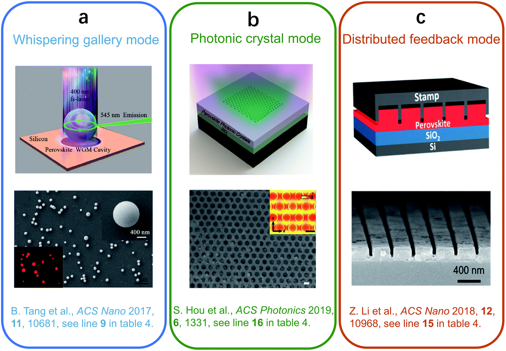 | ||
| Fig. 12 (a) Schematic of perovskite whispering gallery cavity mode laser on silicon substrate and SEM image of CsPbI3 microspheres, reproduced with permission.137 Copyright 2017, American Chemical Society. (b) Schematic of the CsPbBr2.75I0.25 photonic crystal and SEM image of SEM image of a perovskite 2D photonic crystals, reproduced with permission.167 Copyright 2019, American Chemical Society. (c) Schematic of CH3NH3PbI3 distributed feedback mode laser on patterned Si3N4. and SEM micrograph of the device cross section, reproduced with permission.166 Copyright 2018, American Chemical Society. | ||
5.2 Photonic crystal bandedge mode Si-based laser
Photonic crystal bandedge modes are generally established on both edges of a photonic bandgap at high symmetry points in the momentum space. A periodically bunched stationary field profile is the representative characteristic. Perovskite photonic crystal lasers have been reported on Si3N4 waveguide platforms or Si/SiO2 substrate.27,161,162,164 Cha et al. reported perovskite photonic crystal laser on Si3N4 platform.27Fig. 12b presents the schematic of the CH3NH3PbI3 photonic crystal mode laser and SEM image of device cross section. The perovskite laser was realized by spin-coating perovskite film onto the 2D square lattice photonic crystal backbone structure fabricated on Si3N4 platform. The devices exhibit a distinct laser threshold, there is a sharp emission peak on top of broad spontaneous emission. The pulse energy densities of 200 μJ cm−2 at laser threshold are obtained. The perovskite photonic crystals can be well designed on Si-based substrate. Cegielski et al. reported an optically pumped MAPbI3 laser with high-throughput that was fabricated using low cost optical lithography onto a Si3N4 photonic chip.161 The perovskite waveguide is fabricated by spin-coating a liquid perovskite precursor on a Si3N4 photonic chip with a SiO2 cladding layer. A narrow emission spectrum upon a pump threshold fluence of 19.6 μJ cm−2 was observed at room temperature. Fig. 12b shows the schematic and SEM image of a 2D CsPbBr2.75I0.25 photonic crystal which was fabricated by electron beam lithography and reactive ion etching on a Si/SiO2 substrate.167 Both the experiments and simulation further prove that the spontaneous emission rate was enhanced due to photonic bandgap effect which indued by the light energy redistribution from 2D guided modes to vertical direction in perovskite photonic crystals thin films. Compared to unpatterned perovskite films, the light spontaneous emission rate of perovskite photonic crystals is greatly inhibited by 7.9-fold, the PL intensity is enhanced by a factor of 23.5.5.3 Distributed feedback mode Si-based laser
The characteristic of distributed feedback mode laser is Bragg scattering in interference grating which provides optical feedback for the laser. The distributed feedback mode perovskite laser could also be realized by simple progress e.g. spin-coating perovskite film onto patterned substrate. Jia et al. demonstrated distributed feedback perovskite laser constructed on a silicon substrate.159 A gold layer and an Al2O3 layer were pre-deposited between the perovskite and silicon substrate to maximize the thermal conductivity and minimize the surface recombination. A threshold pump intensity of 5 kW cm−2 is obtained for the device. The distributed feedback resonator could be obtained by thermal nanoimprint lithography as shown in Fig. 12c.166 The device achieved an ultralow lasing threshold of 13 W cm−2. At the same time, the same group compared MAPbI3 distributed feedback cavity with the pristine thin film photoluminescence spectrum,165 a 16-fold reduction in emission linewidth was observed. The device with directly patterned perovskite resonator showed room temperature operation. The research of perovskite laser arrays on Si-based photonic nanostructures not only enabled silicon based light sources, but also promoted applications in high throughput bio-sensing and high-resolution displays.6 Conclusions and outlook
Controlling the preparation of perovskite materials on the dominant Si optoelectronics platform is a crucial step to realize perovskite-based practical optoelectronic devices. In recent years, the performance and technology of optoelectronic devices based on the integration of halide perovskite with Si-based materials has been substantially improved. Examples for this successful integration can be found in photovoltaics, photodetection and in light emitting applications. In photovoltaics, the key challenges of integrating the two technologies are related to the different efficiency of optical absorption and the different stability levels achieved so far. Silicon as an indirect band gap material needs to make use of sophisticated light trapping architectures based on micrometer sized pyramidal surface textures to maximize absorption around its band gap in the near infrared. This holds for single junction but also for Si-based tandem solar cells in which the Si has the job of maximizing absorption of low energy photons. Perovskites on the other hand have so far achieved the best efficiencies with solution processed films. Combining both poses challenges that have been overcome e.g. by using smaller pyramids, by only applying the texture to the back surface and by partly using evaporation for perovskite film formation. In terms of perovskite device stability, progress has been made but success is still counted in hundreds or thousands of hours of operation as opposed to decades of lifetime as in Si photovoltaics. Though efficiencies of perovskite/Si tandem solar cells have improved considerably during the last few years, there are still challenges for going towards commercial applications. Textured silicon reduces reflection and enables enhanced light trapping by backscattering, but deposition of thin perovskite layers from solution onto textured silicon with typical pyramid heights of several mm remains a challenge.For photo-FET based perovskite/Si photodetectors, Si was used as gate electrode, SiO2 was used as dielectric. The interface of Si/perovskite heterojunction can promote the separation and transmission of photo-generated carriers, which can not only broaden the light detection range, but also increase the light response rate. Compared with perovskite bulk counterparts, low dimensional perovskite nanocrystals such as 2D perovskites nanosheets, 1D perovskite nanowires and perovskite quantum dots have received increasing attention, mainly due to their potential for integration in photonic circuits. 2D perovskite nanosheets are compatible with the design and fabrication of thin film photoelectronic devices. 1D nanowires show greater application advantages in the metal–semiconductor–metal structure photodetectors than their polycrystalline film counterparts due to higher carrier mobility, and better charge collection. Inorganic halide perovskite quantum dots exhibit higher stability than their organic–inorganic hybrid counterparts. However, low-dimensional perovskite based photodetectors are still in early stage. The structure–property relationships of low dimensional perovskite need further exploring, aiming to make a balance amount of responsivity, stability and cost.
Halide perovskite quantum dots were also employed as emissive layers in LEDs and lasers. Both Si-based perovskite LEDs and perovskite/Si lasers were reported by integrating halide perovskite with silicon-based materials. P-type Si has also been used directly as functional element in LEDs by using it as hole transport layer in perovskite LEDs. These devices demonstrated that using Si as a functional layer can enable high efficiency and good stability in perovskite LEDs. Though Si-based perovskite LEDs have achieved green light emission, red light emission and NIR emission the technology is still at a comparably early stage. Substantial challenges that will be subject of future work are to improve their luminescence quantum efficiency to approach that of LEDs with organic transport layers. Furthermore, like in most perovskite-based applications, the device stability is insufficient. Another urgent problem is to decrease the leakage current and enhanced the light extraction rate.
For perovskite/Si laser, Si-based photonic nanostructures were used as a template to fabricate patterned perovskite laser arrays. The combination of perovskites with Si-based photonic nanostructures has enabled silicon-based light sources. However, the scalable fabrication of patterned single-crystal perovskites is still a challenge, especially for nanostructures with large aspect ratios. In order to obtained perovskite nanolaser arrays with high density and uniform lasing wavelength, the challenge of overcoming the incompatibility of perovskites with the typical lithographic process has to be urgently tackled.
Conflicts of interest
There are no conflicts to declare.Acknowledgements
This work has been partially supported by the National Key R&D Program of China (2018YFC0910600); the National Natural Science Foundation of China (61775145/61525503/61620106016/61835009); Key Project of Department of Education of Guangdong Province (2016KCXTD007); the authors acknowledge also support from the Impuls-und Vernetzungsfonds der Helmholtz Gemeinschaft via the project PEROSEED. We thank J. Hüpkes for carefully reading the manuscript.References
- N. M. Haegel, H. Atwater Jr, T. Barnes, C. Breyer, A. Burrell, Y. M. Chiang, S. D. Wolf, B. Dimmler, D. Feldman, S. Glunz, J. C. Goldschmidt, D. Hochschild, R. Inzunza, I. Kaizuka, B. Kroposki, S. Kurtz, S. Leu, R. Margolis, K. Matsubara, A. Metz, W. K. Metzger, M. Morjaria, S. Niki, S. Nowak, I. M. Peters, S. Philipps, T. Reindl, A. Richter, D. Rose, K. Sakurai, R. Schlatmann, M. Shikano, W. Sinke, R. Sinton, B. J. Stanbery, M. Topic, W. Tumas, Y. Ueda, J. Lagemaat, P. Verlinden, M. Vetter, E. Warren, M. Werner, M. Yamaguchi and A. W. Bett, Science, 2019, 364, 836–838 CrossRef CAS PubMed.
- A. K. Katiyar, K. Y. Thai, W. S. Yun, J. Lee and J. Ahn, Sci. Adv., 2020, 6, b576 Search PubMed.
- A. Goetzberger and C. Hebling, Sol. Energy Mater. Sol. Cells, 2000, 62, 1–19 CrossRef CAS.
- R. Chen, T. D. Tran, K. W. Ng, W. S. Ko, L. C. Chuang, F. G. Sedgwick and C. Chang-Hasnain, Nat. Photonics, 2011, 5, 170–175 CrossRef CAS.
- J. Justice, C. Bower, M. Meitl, M. B. Mooney, M. A. Gubbins and B. Corbett, Nat. Photonics, 2012, 6, 610–614 CrossRef.
- Y. Huang, J. Yan, C. Ma and G. Yang, Nanoscale, 2019, 11, 16299–16307 RSC.
- A. Melianas, F. Etzold, T. J. Savenije, F. Laquai, O. Inganäs and M. Kemerink, Nat. Commun., 2015, 6, 1–8 Search PubMed.
- T. Leijtens, K. A. Bush, R. Prasanna and M. D. McGehee, Nat. Energy, 2018, 3, 828–838 CrossRef CAS.
- E. C. Garnett, B. Ehrler, A. Polman and E. Alarcon-Llado, ACS Photonics, 2021, 8, 61–70 CrossRef CAS PubMed.
- S. Essig, C. Allebé, T. Remo, J. F. Geisz, M. A. Steiner, K. Horowitz, L. Barraud, J. S. Ward, M. Schnabel, A. Descoeudres, D. L. Young, M. Woodhouse, M. Despeisse, C. Ballif and A. Tamboli, Nat. Energy, 2017, 2, 1–9 Search PubMed.
- G. Xing, N. Mathews, S. S. Lim, N. Yantara, X. Liu, D. Sabba, M. Grätzel, S. Mhaisalkar and T. C. Sum, Nat. Mater., 2014, 13, 476–480 CrossRef CAS PubMed.
- D. Shi, V. Adinolfi, R. Comin, M. Yuan, E. Alarousu, A. Buin, Y. Chen, S. Hoogland, A. Rothenberger, K. Katsiev, Y. Losovyj, X. Zhang, P. A. Dowben, O. F. Mohammed, E. H. Sargent and O. M. Bakr, Science, 2015, 347, 519–522 CrossRef CAS PubMed.
- E. Koren, E. Lortscher, C. Rawlings, A. W. Knoll and U. Duerig, Science, 2015, 348, 679–683 CrossRef CAS PubMed.
- Q. Dong, Y. Fang, Y. Shao, P. Mulligan, J. Qiu, L. Cao and J. Huang, Science, 2015, 347, 967–970 CrossRef CAS PubMed.
- N. Wang, L. Cheng, R. Ge, S. Zhang, Y. Miao, W. Zou, C. Yi, Y. Sun, Y. Cao, R. Yang, Y. Wei, Q. Guo, Y. Ke, M. Yu, Y. Jin, Y. Liu, Q. Ding, D. Di, L. Yang, G. Xing, H. Tian, C. Jin, F. Gao, R. H. Friend, J. Wang and W. Huang, Nat. Photonics, 2016, 10, 699–704 CrossRef CAS.
- J. Hebig, I. Kühn, J. Flohre and T. Kirchartz, ACS Energy Lett., 2016, 1, 309–314 CrossRef CAS.
- T. Kirchartz, T. Markvart, U. Rau and D. A. Egger, J. Phys. Chem. Lett., 2018, 9, 939–946 CrossRef CAS PubMed.
- Z. Liu, L. Krückemeier, B. Krogmeier, B. Klingebiel, J. A. Márquez, S. Levcenko, S. Öz, S. Mathur, U. Rau, T. Unold and T. Kirchartz, ACS Energy Lett., 2019, 4, 110–117 CrossRef CAS.
- L. Krückemeier, B. Krogmeier, Z. Liu, U. Rau and T. Kirchartz, Adv. Energy Mater., 2021, 2003489 CrossRef.
- C. C. Boyd, R. Cheacharoen, T. Leijtens and M. D. McGehee, Chem. Rev., 2019, 119, 3418–3451 CrossRef CAS PubMed.
- J. Li, H. L. Cao, W. B. Jiao, Q. Wang, M. Wei, I. Cantone, J. Lü and A. Abate, Nat. Commun., 2020, 11, 310 CrossRef CAS PubMed.
- D. Moia and J. Maier, ACS Energy Lett., 2021, 6, 1566–1576 CrossRef CAS.
- E. Aydin, T. G. Allen, M. De Bastiani, L. Xu, J. Ávila, M. Salvador, E. Van Kerschaver and S. De Wolf, Nat. Commun., 2020, 5, 851–859 CAS.
- T. Kirchartz, S. Korgitzsch, J. Hüpkes, C. O. R. Quiroz and C. J. Brabec, ACS Energy Lett., 2018, 3, 1861–1867 CrossRef CAS.
- J. Liu, X. Sheng, Y. Wu, D. Li, J. Bao, Y. Ji, Z. Lin, X. Xu, L. Yu, J. Xu and K. Chen, Adv. Opt. Mater., 2018, 6, 1700897 CrossRef.
- X. Xu, K. Xiao, G. Hou, Y. Zhang, T. Zhu, L. Xu, J. Xu and K. Chen, Adv. Opt. Mater., 2021, 2100636 CrossRef CAS.
- H. Cha, S. Bae, M. Lee and H. Jeon, Appl. Phys. Lett., 2016, 108, 181104 CrossRef.
- N. Zhang, W. Sun, S. P. Rodrigues, K. Wang, Z. Gu, S. Wang, W. Cai, S. Xiao and Q. Song, Adv. Mater., 2017, 29, 1606205 CrossRef PubMed.
- M. Green, E. Dunlop, J. Hohl-Ebinger, M. Yoshita, N. Kopidakis and X. Hao, Prog. Photovoltaics, 2021, 29, 3–15 Search PubMed.
- T. Kirchartz, Philos. Trans. R. Soc., A, 2019, 377, 20180286 CrossRef PubMed.
- K. Yoshikawa, H. Kawasaki, W. Yoshida, T. Irie, K. Konishi, K. Nakano, T. Uto, D. Adachi, M. Kanematsu, H. Uzu and K. Yamamoto, Nat. Energy, 2017, 2, 17032 CrossRef CAS.
- M. Nakamura, K. Yamaguchi, Y. Kimoto, Y. Yasaki, T. Kato and H. Sugimoto, IEEE J. Photovolt., 2019, 9, 1863 Search PubMed.
- Q. Liu, Y. Jiang, K. Jin, J. Qin, J. Xu, W. Li, J. Xiong, J. Liu, Z. Xiao, K. Sun, S. Yang, X. Zhang and L. Ding, Sci. Bull., 2020, 65, 272 CrossRef CAS.
- O. Almora, D. Baran, G. C. Bazan, C. Berger, C. I. Cabrera, K. R. Catchpole, S. E. Ela, F. Guo, J. Hauch, A. W. Y. Ho-Baillie, T. J. Jacobsson, R. A. J. Janssen, T. Kirchartz, N. Kopidakis, Y. Li, M. A. Loi, R. R. Lunt, X. Mathew, M. D. McGehee, J. Min, D. B. Mitzi, M. K. Nazeeruddin, J. Nelson, A. F. Nogueira, U. W. Paetzold, N. G. Park, B. P. Rand, U. Rau, H. J. Snaith, E. Unger, L. V. Roca, H. L. Yip and C. J. Brabec, Adv. Energy Mater., 2021, 11, 2002774 CrossRef CAS.
- B. M. Kayes, H. Nie, R. Twist, S. G. Spruytte, F. Reinhardt, I. C. Kizilyalli and G. S. Higashi, Proceedings of the 37th IEEE Photovoltaic Specialists Conference (PVSC), 2011, pp. 4–8 Search PubMed.
- First Solar Press Release, First solar achieves yet another cell conversion efficiency world record, 24 February 2016 Search PubMed.
- R. Komiya, A. Fukui, N. Murofushi, N. Koide, R. Yamanaka and H. Katayama, Technical Digest, 21st International Photovoltaic Science and Engineering Conference, 2011, November, 2C-5O-08 Search PubMed.
- M. Jeong, I. W. Choi, E. M. Go, Y. Cho, M. Kim, B. Lee, S. Jeong, Y. Jo, H. W. Choi, J. Lee, J. H. Bae, S. K. Kwak, D. S. Kim and C. Yang, Science, 2020, 369, 1615–1620 CrossRef CAS PubMed.
- H. Sai, T. Matsui, H. Kumagai and K. Matsubara, Appl. Phys. Express, 2018, 11, 022301 CrossRef.
- L. Krückemeier, U. Rau, M. Stolterfoht and T. Kirchartz, Adv. Energy Mater., 2020, 10, 1902573 CrossRef.
- T. Kirchartz and U. Rau, Adv. Energy Mater., 2018, 8, 1703385 CrossRef.
- M. Jošt, E. Köhnen, A. B. Morales-Vilches, B. Lipovšek, K. Jäger, B. Macco, A. Al-Ashouri, J. Krč, L. Korte, B. Rech, R. Schlatmann, M. Topič, B. Stannowski and S. Albrecht, Energy Environ. Sci., 2018, 11, 3511–3523 RSC.
- F. Sahli, J. Werner, B. A. Kamino, M. Bräuninger, R. Monnard, B. Paviet-Salomon, L. Barraud, L. Ding, J. J. Diaz Leon, D. Sacchetto, G. Cattaneo, M. Despeisse, M. Boccard, S. Nicolay, Q. Jeangros, B. Niesen and C. Ballif, Nat. Mater., 2018, 17, 820–826 CrossRef CAS PubMed.
- J. J. Yoo, G. Seo, M. R. Chua, T. G. Park, Y. l. Lu, F. Rotermund, Y. K. Kim, C. Su Moon, N. J. Jeon, J. P. C. Baena, V. Bulović, S. S. Shin, M. G. Bawendi and J. Seo, Nature, 2021, 590, 587–593 CrossRef CAS PubMed.
- J. Jeong, M. Kim, J. Seo, H. Lu, P. Ahlawat, A. Mishra, Y. Yang, M. A. Hope, F. T. Eickemeyer, M. Kim, Y. J. Yoon, I. W. Choi, B. P. Darwich, S. J. Choi, Y. Jo, J. H. Lee, B. Walker, S. M. Zakeeruddin, L. Emsley, U. Rothlisberger, A. Hagfeldt, D. S. Kim, M. Grätzel and J. Y. Kim, Nature, 2021, 592, 381–385 CrossRef CAS PubMed.
- A. Richter, R. Müller, J. Benick, F. Feldmann1, B. Steinhauser, C. Reichel, A. Fell, M. Bivour, M. Hermle and S. W. Glunz, Nat. Energy, 2021, 6, 429–438 CrossRef CAS.
- A. R. Bowman, F. Lang, Y. Chiang, A. Jiménez-Solano, K. Frohna, G. E. Eperon, E. Ruggeri, M. Abdi-Jalebi, M. Anaya, B. V. Lotsch and S. D. Stranks, ACS Energy Lett., 2021, 6, 612–620 CrossRef CAS PubMed.
- A. Pusch, P. Pearce and N. J. Ekins-Daukes, IEEE J. Photovolt., 2019, 3, 679–687 Search PubMed.
- B. Ehrler, E. Alarcón-Lladó, S. W. Tabernig, T. Veeken, E. C. Garnett and A. Polman, ACS Energy Lett., 2020, 5, 3029–3033 CrossRef CAS.
- M. Jošt, L. Kegelmann, L. Korte and S. Albrecht, Adv. Energy Mater., 2020, 10, 1904102 CrossRef.
- H. Shen, D. Walter, Y. Wu, K. C. Fong, D. A. Jacobs, T. Duong, J. Peng, K. Weber, T. P. White and K. R. Catchpole, Adv. Energy Mater., 2020, 10, 1902840 CrossRef CAS.
- A. Richter, R. Müller, J. Benick, F. Feldmann, B. Steinhauser, C. Reichel, A. Fell, M. Bivour, M. Hermle and S. W. Glunz, Nat. Energy, 2021, 6, 429 CrossRef CAS.
- A. Al-Ashouri, E. Köhnen, B. Li, A. Magomedov, H. Hempel, P. Caprioglio, J. A. Márquez, A. B. M. Vilches, E. Kasparavicius, J. A. Smith, N. Phung, D. Menzel, M. Grischek, L. Kegelmann, D. Skroblin, C. Gollwitzer, T. Malinauskas, M. Jošt, G. Matic, B. Rech, R. Schlatmann, M. Topic, L. Korte, A. Abate, B. Stannowski, D. Neher, M. Stolterfoht, T. Unold, V. Getautis and S. Albrecht, Science, 2020, 370, 1300–1309 CrossRef CAS PubMed.
- R. Fan, N. Zhou, L. Zhang, R. Yang, Y. Meng, L. Li, T. Guo, Y. Chen, Z. Xu, G. Zheng, Y. Huang, L. Li, L. Qin, X. Qiu, Q. Chen and H. Zhou, Sol. RRL, 2017, 1, 1700149 CrossRef.
- Y. Wu, D. Yan, J. Peng, T. Duong, Y. Wan, S. P. Phang, H. Shen, N. Wu, C. Barugkin, X. Fu, S. Surve, D. Grant, D. Walter, T. P. White, K. R. Catchpole and K. J. Weber, Energy Environ. Sci., 2017, 10, 2472–2479 RSC.
- K. A. Bush, A. F. Palmstrom, Z. J. Yu, M. Boccard, R. Cheacharoen, J. P. Mailoa, D. P. McMeekin, R. L. Z. Hoye, C. D. Bailie, T. Leijtens, I. M. Peters, M. C. Minichetti, N. Rolston, R. Prasanna, S. Sofia, D. Harwood, W. Ma, F. Moghadam, H. J. Snaith, T. Buonassisi, Z. C. Holman, S. F. Bent and M. D. McGehee, Nat. Energy, 2017, 2, 17009 CrossRef CAS.
- S. Zhu, F. Hou, W. Huang, X. Yao, B. Shi, Q. Ren, J. Chen, L. Yan, S. An, Z. Zhou, H. Ren, C. Wei, Q. Huang, Y. Li, G. Hou, X. Chen, Y. Ding, G. Wang, B. Li, Y. Zhao and X. Zhang, Sol. RRL, 2018, 2, 1800176 CrossRef.
- Z. Qiu, Z. Xu, N. Li, N. Zhou, Y. Chen, X. Wan, J. Liu, N. Li, X. Hao, P. Bi, Q. Chen, B. Cao and H. Zhou, Nano Energy, 2018, 53, 798–807 CrossRef CAS.
- K. A. Bush, S. Manzoor, K. Frohna, Z. J. Yu, J. A. Raiford, A. F. Palmstrom, H. Wang, R. Prasanna, S. F. Bent, Z. C. Holman and M. D. McGehee, ACS Energy Lett., 2018, 3, 2173–2180 CrossRef CAS.
- L. Mazzarella, Y. H. Lin, S. Kirner, A. B. Morales Vilches, L. Korte, S. Albrecht, E. Crossland, B. Stannowski, C. Case, H. J. Snaith and R. Schlatmann, Adv. Energy Mater., 2019, 9, 1803241 CrossRef.
- C. U. Kim, J. C. Yu, E. D. Jung, I. Y. Choi, W. Park, H. Lee, I. Kim, D. Lee, K. K. Hong, M. H. Song and K. J. Choi, Nano Energy, 2019, 60, 213–221 CrossRef CAS.
- E. Kohnen, M. Jǒst, A. B. Morales-Vilches, P. Tockhorn, A. Al-Ashouri, B. Macco, L. Kegelmann, B. Rech, R. Schlatmann, B. Stannowski and S. Albrecht, Sustainable Energy Fuels, 2019, 3, 1995–2005 RSC.
- B. Chen, Z. Yu, K. Liu, X. Zheng, Y. Liu, J. Shi, D. Spronk, P. N. Rudd, Z. Holman and J. Huang, Joule, 2019, 3, 177–190 CrossRef CAS.
- Y. Hou, E. Aydin, M. De Bastiani, C. Xiao, F. H. Isikgor, D. Xue, B. Chen, H. Chen, B. Bahrami, A. H. Chowdhury, A. Johnston, S. Baek, Z. Huang, M. Wei, Y. Dong, J. Troughton, R. Jalmood, A. J. Mirabelli, T. G. Allen, E. Van Kerschaver, M. I. Saidaminov, D. Baran, Q. Qiao, K. Zhu, S. De Wolf and E. H. Sargent, Science, 2020, 367, 1135–1140 CrossRef CAS PubMed.
- E. Lamanna, F. Matteocci, E. Calabrò, L. Serenelli, E. Salza, L. Martini, F. Menchini, M. Izzi, A. Agresti, S. Pescetelli, S. Bellani, A. E. Del Río Castillo, F. Bonaccorso, M. Tucci and A. Di Carlo, Joule, 2020, 4, 865–881 CrossRef CAS.
- D. Kim, H. J. Jung, I. J. Park, B. W. Larson, S. P. Dunfield, C. Xiao, J. Kim, J. Tong, P. Boonmongkolras, S. G. Ji, F. Zhang, S. R. Pae, M. Kim, S. B. Kang, V. Dravid, J. J. Berry, J. Y. Kim, K. Zhu, D. H. Kim and B. Shin, Science, 2020, 368, 155–160 CrossRef CAS PubMed.
- K. Wang, G. Xing, Q. Song and S. Xiao, Adv. Mater., 2020, 2000306 Search PubMed.
- G. E. Eperon, M. T. Hörantner and H. J. Snaith, Nat. Rev. Chem., 2017, 1, 0095 CrossRef CAS.
- S. Albrecht and B. Rech, Nat. Commun., 2017, 2, 16196 Search PubMed.
- J. J. Yoo, S. Wieghold, M. C. Sponseller, M. R. Chua, S. N. Bertram, N. T. P. Hartono, J. S. Tresback, E. C. Hansen, J. Correa-Baena, V. Bulović, T. Buonassisi, S. S. Shin and M. G. Bawendi, Energy Environ. Sci., 2019, 12, 2192–2199 RSC.
- Q. Jiang, Y. Zhao, X. Zhang, X. Yang, Y. Chen, Z. Chu, Q. Ye, X. Li, Z. Yin and J. You, Nat. Photonics, 2019, 13, 460–466 CrossRef CAS.
- X. Zheng, Y. Hou, C. Bao, J. Yin, F. Yuan, Z. Huang, K. Song, J. Liu, J. Troughton, N. Gasparini, C. Zhou, Y. Lin, D. Xue, B. Chen, A. K. Johnston, N. Wei, M. N. Hedhili, M. Wei, A. Y. Alsalloum, P. Maity, B. Turedi, C. Yang, D. Baran, T. D. Anthopoulos, Y. Han, Z. Lu, O. F. Mohammed, F. Gao, E. H. Sargent and O. M. Bakr, Nat. Commun., 2020, 5, 131–140 CAS.
- Z. Liu, J. Siekmann, B. Klingebiel, U. Rau and T. Kirchartz, Adv. Energy Mater., 2021, 2003386 CrossRef CAS.
- D. P. McMeekin, G. Sadoughi, W. Rehman, G. E. Eperon, M. Saliba, M. T. Hörantner, A. Haghighirad, N. Sakai, L. Korte, B. Rech, M. B. Johnston, L. M. Herz and H. J. Snaith, Science, 2016, 351, 151–155 CrossRef CAS PubMed.
- J. Xu, C. C. Boyd, Z. J. Yu, A. F. Palmstrom, D. J. Witter, B. W. Larson, R. M. France, J. Werner, S. P. Harvey, E. J. Wolf, W. Weigand, S. Manzoor, M. F. A. M. van Hest, J. J. Berry, J. M. Luther, Z. C. Holman and M. D. McGehee, Science, 2020, 367, 1097–1104 CrossRef CAS PubMed.
- J. P. Mailoa, C. D. Bailie, E. C. Johlin, E. T. Hoke, A. J. Akey, W. H. Nguyen, M. D. McGehee and T. Buonassisi, Appl. Phys. Lett., 2015, 106, 121105 CrossRef.
- M. Köhler, M. Pomaska, P. Procel, R. Santbergen, A. Zamchiy, B. Macco, A. Lambertz, W. Duan, P. Cao, B. Klingebiel, S. Li, A. Eberst, M. Luysberg, K. Qiu, O. Isabella, F. Finger, T. Kirchartz, U. Rau and K. Ding, Nat. Energy, 2021, 6, 529 CrossRef.
- G. Nogay, F. Sahli, J. Werner, R. Monnard, M. Boccard, M. Despeisse, F. J. Haug, Q. Jeangros, A. Ingenito and C. Ballif, ACS Energy Lett., 2019, 4, 844–845 CrossRef CAS.
- B. Chen, Z. J. Yu, S. Manzoor, S. Wang, W. Weigand, Z. Yu, G. Yang, Z. Ni, X. Dai, Z. C. Holman and J. Huang, Joule, 2020, 4, 850–864 CrossRef CAS.
- L. Zhou, R. Wang, C. Yao, X. Li, C. Wang, X. Zhang, C. Xu, A. Zeng, D. Zhao and F. Zhang, Nat. Commun., 2015, 6, 6938 CrossRef CAS PubMed.
- A. Armin, R. D. Jansen-van Vuuren, N. Kopidakis, P. L. Burn and P. Meredith, Nat. Commun., 2015, 6, 6343 CrossRef CAS PubMed.
- R. D. Jansen-van Vuuren, A. Armin, A. K. Pandey, P. L. Burn and P. Meredith, Adv. Mater., 2016, 28, 4766–4802 CrossRef CAS PubMed.
- F. H. L. Koppens, T. Mueller, P. Avouris, A. C. Ferrari, M. S. Vitiello and M. Polini, Nat. Nanotechnol., 2014, 9, 780–793 CrossRef CAS PubMed.
- J. Liu, Y. Xue, Z. Wang, Z. Xu, C. Zheng, B. Weber, J. Song, Y. Wang, Y. Lu, Y. Zhang and Q. Bao, ACS Nano, 2016, 10, 3536–3542 CrossRef CAS PubMed.
- W. Deng, X. Zhang, L. Huang, X. Xu, L. Wang, J. Wang, Q. Shang, S. Lee and J. Jie, Adv. Mater., 2016, 28, 2201–2208 CrossRef CAS PubMed.
- H. Deng, X. Yang, D. Dong, B. Li, D. Yang, S. Yuan, K. Qiao, Y. Cheng, J. Tang and H. Song, Nano Lett., 2015, 15, 7963–7969 CrossRef CAS PubMed.
- J. Song, L. Xu, J. Li, J. Xue, Y. Dong, X. Li and H. Zeng, Adv. Mater., 2016, 28, 4861–4868 CrossRef CAS PubMed.
- X. Li, D. Yu, F. Cao, Y. Gu, Y. Wei, Y. Wu, J. Song and H. Zeng, Adv. Funct. Mater., 2016, 26, 5903–5912 CrossRef CAS.
- A. Waleed, M. M. Tavakoli, L. Gu, Z. Wang, D. Zhang, A. Manikandan, Q. Zhang, R. Zhang, Y. Chueh and Z. Fan, Nano Lett., 2016, 17, 523–530 CrossRef PubMed.
- D. H. Kwak, D. H. Lim, H. S. Ra, P. Ramasamy and J. S. Lee, RSC Adv., 2016, 6, 65252–65256 RSC.
- M. Shoaib, X. Zhang, X. Wang, H. Zhou, T. Xu, X. Wang, X. Hu, H. Liu, X. Fan, W. Zheng, T. Yang, S. Yang, Q. Zhang, X. Zhu, L. Sun and A. Pan, J. Am. Chem. Soc., 2017, 139, 15592–15595 CrossRef CAS PubMed.
- W. Deng, L. Huang, X. Xu, X. Zhang, X. Jin, S. Lee and J. Jie, Nano Lett., 2017, 17, 2482–2489 CrossRef CAS PubMed.
- X. Liu, D. Yu, F. Cao, X. Li, J. Ji, J. Chen, X. Song and H. Zeng, Small, 2017, 13, 1700364 CrossRef PubMed.
- Y. Chen, Y. Chu, X. Wu, W. Ou-Yang and J. Huang, Adv. Mater., 2017, 29, 1704062 CrossRef PubMed.
- T. Yang, Y. Zheng, Z. Du, W. Liu, Z. Yang, F. Gao, L. Wang, K. Chou, X. Hou and W. Yang, ACS Nano, 2018, 12, 1611–1617 CrossRef CAS PubMed.
- J. Feng, C. Gong, H. Gao, W. Wen, Y. Gong, X. Jiang, B. Zhang, Y. Wu, Y. Wu, H. Fu, L. Jiang and X. Zhang, Nat. Electron., 2018, 1, 404–410 CrossRef CAS.
- H. Wu, H. Si, Z. Zhang, Z. Kang, P. Wu, L. Zhou, S. Zhang, Z. Zhang, Q. Liao and Y. Zhang, Adv. Sci., 2018, 5, 1801219 CrossRef PubMed.
- W. Zhai, J. Lin, C. Li, S. Hu, Y. Huang, C. Yu, Z. Wen, Z. Liu, Y. Fang and C. Tang, Nanoscale, 2018, 10, 21451–21458 RSC.
- Y. Zhou, J. Luo, Y. Zhao, C. Ge, C. Wang, L. Gao, C. Zhang, M. Hu, G. Niu and J. Tang, Adv. Opt. Mater., 2018, 6, 1800679 CrossRef.
- B. Pradhan, G. S. Kumar, S. Sain, A. Dalui, U. K. Ghorai, S. K. Pradhan and S. Acharya, Chem. Mater., 2018, 30, 2135–2142 CrossRef CAS.
- Y. Meng, C. Lan, F. Li, S. Yip, R. Wei, X. Kang, X. Bu, R. Dong, H. Zhang and J. C. Ho, ACS Nano, 2019, 13, 6060–6070 CrossRef CAS PubMed.
- Y. Zhao, Y. Qiu, H. Gao, J. Feng, G. Chen, L. Jiang and Y. Wu, Adv. Mater., 2020, 32, 1905298 CrossRef CAS PubMed.
- G. Chen, J. Feng, H. Gao, Y. Zhao, Y. Pi, X. Jiang, Y. Wu and L. Jiang, Adv. Funct. Mater., 2019, 29, 1808741 CrossRef.
- Y. Yang, H. Dai, F. Yang, Y. Zhang, D. Luo, X. Zhang, K. Wang, X. W. Sun and J. Yao, Nanoscale Res. Lett., 2019, 14, 291 CrossRef PubMed.
- M. Gong, R. Sakidja, R. Goul, D. Ewing, M. Casper, A. Stramel, A. Elliot and J. Z. Wu, ACS Nano, 2019, 13, 1772–1783 CrossRef CAS PubMed.
- T. Yang, X. Wang, B. Zheng, Z. Qi, C. Ma, Y. Fu, Y. Fu, M. P. Hautzinger, Y. Jiang, Z. Li, P. Fan, F. Li, W. Zheng, Z. Luo, J. Liu, B. Yang, S. Chen, D. Li, L. Zhang, S. Jin and A. Pan, ACS Nano, 2019, 13, 7996–8003 CrossRef CAS PubMed.
- S. Parveen, K. K. Paul and P. K. Giri, ACS Appl. Mater. Interfaces, 2020, 12, 6283–6297 CrossRef CAS PubMed.
- W. Niu, A. Eiden, G. Vijaya Prakash and J. J. Baumberg, Appl. Phys. Lett., 2014, 104, 171111 CrossRef.
- Q. Zhang, S. T. Ha, X. Liu, T. C. Sum and Q. Xiong, Nano Lett., 2014, 14, 5995–6001 CrossRef CAS PubMed.
- R. Su, C. Diederichs, J. Wang, T. C. H. Liew, J. Zhao, S. Liu, W. Xu, Z. Chen and Q. Xiong, Nano Lett., 2017, 17, 3982–3988 CrossRef CAS PubMed.
- S. T. Ha, X. Liu, Q. Zhang, D. Giovanni, T. C. Sum and Q. Xiong, Adv. Opt. Mater., 2014, 2, 838–844 CrossRef CAS.
- Q. Liao, K. Hu, H. Zhang, X. Wang, J. Yao and H. Fu, Adv. Mater., 2015, 27, 3405–3410 CrossRef CAS PubMed.
- Y. Gao, E. Shi, S. Deng, S. B. Shiring, J. M. Snaider, C. Liang, B. Yuan, R. Song, S. M. Janke, A. Liebman-Peláez, P. Yoo, M. Zeller, B. W. Boudouris, P. Liao, C. Zhu, V. Blum, Y. Yu, B. M. Savoie, L. Huang and L. Dou, Nat. Chem., 2019, 11, 1151–1157 CrossRef CAS PubMed.
- J. Feng, X. Yan, Y. Liu, H. Gao, Y. Wu, B. Su and L. Jiang, Adv. Mater., 2017, 29, 1605993 CrossRef PubMed.
- K. Hong, Q. V. Le, S. Y. Kim and H. W. Jang, J. Mater. Chem. C, 2018, 6, 2189–2229 RSC.
- L. Gao, K. Zeng, J. Guo, C. Ge, J. Du, Y. Zhao, C. Chen, H. Deng, Y. He, H. Song, G. Niu and J. Tang, Nano Lett., 2016, 16, 7446–7454 CrossRef CAS PubMed.
- L. Zhu, Q. Lai, W. Zhai, B. Chen and Z. L. Wang, Mater. Today, 2020, 37, 56–63 CrossRef CAS.
- D. H. Lim, P. Ramasamy, D. H. Kwak and J. S. Lee, Nanotechnology, 2017, 28, 255601 CrossRef PubMed.
- D. Zhang, Y. Yang, Y. Bekenstein, Y. Yu, N. A. Gibson, A. B. Wong, S. W. Eaton, N. Kornienko, Q. Kong, M. Lai, A. P. Alivisatos, S. R. Leone and P. Yang, J. Am. Chem. Soc., 2016, 138, 7236–7239 CrossRef CAS PubMed.
- X. He, P. Liu, S. Wu, Q. Liao, J. Yao and H. Fu, J. Mater. Chem. C, 2017, 5, 12707 RSC.
- J. K. Meyers, S. Kim, D. J. Hill, E. E. M. Cating, L. J. Williams, A. S. Kumbhar, J. R. McBride, J. M. Papanikolas and J. F. Cahoon, Nano Lett., 2017, 17, 7561–7568 CrossRef CAS PubMed.
- C. Bao, J. Yang, S. Bai, W. Xu, Z. Yan, Q. Xu, J. Liu, W. Zhang and F. Gao, Adv. Mater., 2018, 30, 1803422 CrossRef PubMed.
- F. Liu, Y. Zhang, C. Ding, S. Kobayashi, T. Izuishi, N. Nakazawa, T. Toyoda, T. Ohta, S. Hayase, T. Minemoto, K. Yoshino, S. Dai and Q. Shen, ACS Nano, 2017, 11, 10373–10383 CrossRef CAS PubMed.
- Y. Wang and H. Sun, Small Methods, 2018, 2, 1700252 CrossRef.
- P. Ramasamy, D. Lim, B. Kim, S. Lee, M. Lee and J. Lee, Chem. Commun., 2016, 52, 2067–2070 RSC.
- J. Lu, X. Sheng, G. Tong, Z. Yu, X. Sun, L. Yu, X. Xu, J. Wang, J. Xu, Y. Shi and K. Chen, Adv. Mater., 2017, 29, 1700400 CrossRef PubMed.
- L. Protesescu, S. Yakunin, M. I. Bodnarchuk, F. Krieg, R. Caputo, C. H. Hendon, R. X. Yang, A. Walsh and M. V. Kovalenko, Nano Lett., 2015, 15, 3692–3696 CrossRef CAS PubMed.
- G. Li, F. W. R. Rivarola, N. J. L. K. Davis, S. Bai, T. C. Jellicoe, F. de la Peña, S. Hou, C. Ducati, F. Gao, R. H. Friend, N. C. Greenham and Z. Tan, Adv. Mater., 2016, 28, 3528–3534 CrossRef CAS PubMed.
- W. Xu, Q. Hu, S. Bai, C. Bao, Y. Miao, Z. Yuan, T. Borzda, A. J. Barker, E. Tyukalova, Z. Hu, M. Kawecki, H. Wang, Z. Yan, X. Liu, X. Shi, K. Uvdal, M. Fahlman, W. Zhang, M. Duchamp, J. Liu, A. Petrozza, J. Wang, L. Liu, W. Huang and F. Gao, Nat. Photonics, 2019, 13, 418–424 CrossRef CAS.
- T. Chiba1, Y. Hayashi, H. Ebe, K. Hoshi, J. Sato, S. Sato, Y. J. Pu, S. Ohisa and J. Kido, Nat. Photonics, 2018, 12, 681–687 CrossRef.
- Y. Dong, Y. K. Wang, F. Yuan, A. Johnston, Y. Liu, D. Ma, M.-J. Choi, B. Chen, M. Chekini, S.-W. Baek, L. K. Sagar, J. Fan, Y. Hou, M. Wu, S. Lee, B. Sun, S. Hoogland, R. Quintero-Bermudez, H. Ebe, P. Todorovic, F. Dinic, P. Li, H. T. Kung, M. I. Saidaminov, E. Kumacheva, E. Spiecker, L.-S. Liao, O. Voznyy, Z. H. Lu and E. H. Sargent, Nat. Nanotechnol., 2020, 15, 668–674 CrossRef CAS PubMed.
- J. Liu, X. Zhang, Y. Ji, X. Sheng, H. Ma, X. Xu, L. Yu, J. Xu and K. Chen, Adv. Opt. Mater., 2018, 6, 1800693 CrossRef.
- J. Liu, Z. Lu, X. Zhang, Y. Zhang, H. Ma, Y. Ji, X. Xu, L. Yu, J. Xu and K. Chen, Nanomaterials, 2018, 8, 974 CrossRef PubMed.
- X. Liu, D. Yu, C. Huo, X. Song, Y. Gao, S. Zhang and H. Zeng, Adv. Opt. Mater., 2018, 1800206 CrossRef.
- Q. Zhang, R. Su, X. Liu, J. Xing, T. C. Sum and Q. Xiong, Adv. Funct. Mater., 2016, 26, 6238–6245 CrossRef CAS.
- H. Zhu, Y. Fu, F. Meng, X. Wu, Z. Gong, Q. Ding, M. V. Gustafsson, M. T. Trinh, S. Jin and X. Zhu, Nat. Mater., 2015, 14, 636–642 CrossRef CAS PubMed.
- B. Tang, H. Dong, L. Sun, W. Zheng, Q. Wang, F. Sun, X. Jiang, A. Pan and L. Zhang, ACS Nano, 2017, 11, 10681–10688 CrossRef CAS PubMed.
- K. Wang, S. Sun, C. Zhang, W. Sun, Z. Gu, S. Xiao and Q. Song, Mater. Chem. Front., 2017, 1, 477–481 RSC.
- N. Pourdavoud, T. Haeger, A. Mayer, P. J. Cegielski, A. L. Giesecke, R. Heiderhoff, S. Olthof, S. Zaefferer, I. Shutsko, A. Henkel, D. Becker-Koch, M. Stein, M. Cehovski, O. Charfi, H. Johannes, D. Rogalla, M. C. Lemme, M. Koch, Y. Vaynzof, K. Meerholz, W. Kowalsky, H. Scheer, P. Görrn and T. Riedl, Adv. Mater., 2019, 31, 1903717 CrossRef PubMed.
- H. Cha, S. Bae, H. Jung, M. J. Ko and H. Jeon, Adv. Opt. Mater., 2017, 5, 1700545 CrossRef.
- J. Zhao, Y. Yan, C. Wei, W. Zhang, Z. Gao and Y. S. Zhao, Nano Lett., 2018, 18, 1241–1245 CrossRef CAS PubMed.
- K. Wang, W. Sun, J. Li, Z. Gu, S. Xiao and Q. Song, ACS Photonics, 2016, 3, 1125–1280 CrossRef CAS.
- H. Dong, C. Zhang, X. Liu, J. Yaoab and Y. S. Zhao, Chem. Soc. Rev., 2020, 49, 951–982 RSC.
- Q. Shang, M. Li, L. Zhao, D. Chen, S. Zhang, S. Chen, P. Gao, C. Shen, J. Xing, G. Xing, B. Shen, X. Liu and Q. Zhang, Nano Lett., 2020, 20, 6636–6643 CrossRef CAS PubMed.
- Q. Zhang, Q. Shuang, R. Su, T. T. H. Do and Q. Xiong, Nano Lett., 2021, 21, 1903–1914 CrossRef CAS PubMed.
- D. H. Nguyen, J. Y. Sun, C. Y. Lo, J. M. Liu, W. S. Tsai, M. H. Li, S. J. Yang, C. C. Lin, S. D. Tzeng, Y. R. Ma, M. Y. Lin and C. C. Lai, Adv. Mater., 2021, 33, 2006819 CrossRef CAS PubMed.
- L. Lei, Q. Dong, K. Gundogdu and F. So, Adv. Funct. Mater., 2021, 31, 2010144 CrossRef CAS.
- F. Deschler, M. Price, S. Pathak, L. E. Klintberg, D. Jarausch, R. Higler, S. Hüttner, T. Leijtens, S. D. Stranks, H. J. Snaith, M. Atatüre, R. T. Phillips and R. H. Friend, J. Phys. Chem. Lett., 2014, 5, 1421–1426 CrossRef CAS PubMed.
- T. S. Kao, Y. Hong, K. Hong and T. Lu, Nanotechnology, 2021, 32, 282001 CrossRef CAS PubMed.
- P. Brenner, M. Stulz, D. Kapp, T. Abzieher, U. W. Paetzold, A. Quintilla, I. A. Howard, H. Kalt and U. Lemmer, Appl. Phys. Lett., 2016, 109, 141106 CrossRef.
- A. Pan, W. Zhou, E. S. P. Leong, R. Liu, A. H. Chin, B. Zou and C. Z. Ning, Nano Lett., 2009, 9, 784–788 CrossRef CAS PubMed.
- Y. S. Zhao, A. Peng, H. Fu, Y. Ma and J. Yao, Adv. Mater., 2008, 20, 1661–1665 CrossRef CAS.
- T. Rauch, M. Böberl, S. F. Tedde, J. Fürst, M. V. Kovalenko, G. Hesser, U. Lemmer, W. Heiss and O. Hayden, Nat. Photonics, 2009, 3, 332 CrossRef CAS.
- D. Xing, C. C. Lin, Y. L. Ho, A. S. A. Kamal, I. T. Wang, C. C. Chen, C. Y. Wen, C. W. Chen and J. J. Delaunay, Adv. Funct. Mater., 2020, 31, 2006283 CrossRef.
- B. R. Sutherland, S. Hoogland, M. M. Adachi, C. T. O. Wong and E. H. Sargent, ACS Nano, 2014, 8, 10947 CrossRef CAS PubMed.
- S. Yakunin, L. Protesescu, F. Krieg, M. I. Bodnarchuk, G. Nedelcu, M. Humer, G. De Luca, M. Fiebig, W. Heiss and M. V. Kovalenko, Nat. Commun., 2015, 6, 8056 CrossRef CAS PubMed.
- X. Liu, L. Niu, C. Wu, C. Cong, H. Wang, Q. Zeng, H. He, Q. Fu, W. Fu, T. Yu, C. Jin, Z. Liu and T. C. Sum, Adv. Sci., 2016, 3, 1600137 CrossRef PubMed.
- K. Wang, Z. Gu, S. Liu, W. Sun, N. Zhang, S. Xiao and Q. Song, J. Phys. Chem. Lett., 2016, 7, 2549–2555 CrossRef CAS PubMed.
- Y. Jia, R. A. Kerner, A. J. Grede, A. N. Brigeman, B. P. Rand and N. C. Giebink, Nano Lett., 2016, 16, 4624–4629 CrossRef CAS PubMed.
- Z. Duan, Y. Wang, G. Li, S. Wang, N. Yi, S. Liu, S. Xiao and Q. Song, Laser Photonics Rev., 2017, 12, 1700234 CrossRef.
- P. J. Cegielski, S. Neutzner, C. Porschatis, H. Lerch, J. Bolten, S. Suckow, A. R. S. Kandada, B. Chmielak, A. Petrozza, T. Wahlbrink and A. L. Giesecke, Opt. Express, 2017, 25, 13199 CrossRef CAS PubMed.
- Z. Yang, M. Pelton, M. I. Bodnarchuk, M. V. Kovalenko and E. Waks, Appl. Phys. Lett., 2017, 111, 221104 CrossRef.
- P. J. Cegielski, A. L. Giesecke, S. Neutzner, C. Porschatis, M. Gandini, D. Schall, C. A. R. Perini, J. Bolten, S. Suckow, S. Kataria, B. Chmielak, T. Wahlbrink, A. Petrozza and M. C. Lemme, Nano Lett., 2018, 18, 6915–6923 CrossRef CAS PubMed.
- Q. Shang, S. Zhang, Z. Liu, J. Chen, P. Yang, C. Li, W. Li, Y. Zhang, Q. Xiong, X. Liu and Q. Zhang, Nano Lett., 2018, 18, 3335–3343 CrossRef CAS PubMed.
- A. Gharajeh, R. Haroldson, Z. Li, J. Moon, B. Balachandran, W. Hu, A. Zakhidov and Q. Gu, Opt. Lett., 2018, 43, 611–614 CrossRef CAS PubMed.
- Z. Li, J. Moon, A. Gharajeh, R. Haroldson, R. Hawkins, W. Hu, A. Zakhidov and Q. Gu, ACS Nano, 2018, 12, 10968–10976 CrossRef CAS PubMed.
- S. Hou, A. Xie, Z. Xie, L. Y. M. Tobing, J. Zhou, L. Tjahjana, J. Yu, C. Hettiarachchi, D. Zhang, C. Dang, E. H. T. Teo, M. D. Birowosuto and H. Wang, ACS Photonics, 2019, 6, 1331–1337 CrossRef CAS.
- M. B. Price, K. Lewellen, J. Hardy, S. M. Lockwood, C. Zemke-Smith, I. Wagner, M. Gao, J. Grand, K. Chen, J. M. Hodgkiss, E. L. Ru and N. J. L. K. Davis, J. Phys. Chem. Lett., 2020, 11, 7009–7014 CrossRef CAS PubMed.
- H. Yu, X. Xu, H. Liu, Y. Wan, X. Cheng, J. Chen, Y. Ye and L. Dai, ACS Nano, 2020, 14, 552–558 CrossRef CAS PubMed.
- X. He, P. Liu, H. Zhang, Q. Liao, J. Yao and H. Fu, Adv. Mater., 2017, 29, 1604510 CrossRef PubMed.
| This journal is © The Royal Society of Chemistry 2021 |