
Ultrathin 2D/2D Ti3C2Tx/semiconductor dual-functional photocatalysts for simultaneous imine production and H2 evolution†
Hao
Wang
a,
Peng
Hu
a,
Jie
Zhou
a,
Maarten B. J.
Roeffaers
 c,
Bo
Weng
*c,
Yongqing
Wang
*a and
Hongbing
Ji
*ab
c,
Bo
Weng
*c,
Yongqing
Wang
*a and
Hongbing
Ji
*ab
aFine Chemical Industry Research Institute, School of Chemistry, Sun Yat-sen University, Guangzhou, 510275, P. R. China. E-mail: wangyq223@mail.sysu.edu.cn; jihb@mail.sysu.edu.cn
bSchool of Chemical Engineering, Guangdong University of Petrochemical Technology, Maoming, 525000, P. R. China
ccMACS, Department of Microbial and Molecular Systems, KU Leuven, Celestijnenlaan 200F, 3001, Leuven, Belgium. E-mail: bo.weng@kuleuven.be
First published on 13th July 2021
Abstract
Ultrathin 2D/2D Ti3C2Tx/semiconductor (CdS and Bi2MoO6) dual-functional photocatalysts have been constructed for the oxidative coupling of benzylamines to imines combined with H2 generation under visible light irradiation (λ ≥420 nm). The optimal 2D/2D Ti3C2Tx/CdS sample exhibits high photocatalytic performance toward H2 evolution (219.7 μmol g−1 h−1) and imine production (155.8 μmol g−1 h−1), which is 5 times and 6 times higher than that of pure CdS, respectively. In situ irradiated XPS and photoelectrochemical characterizations reveal that the enhanced photoactivity over Ti3C2Tx/semiconductor heterostructures can be attributed to the facilitated charge separation from the semiconductors to the Ti3C2Tx cocatalyst. A possible reaction mechanism is proposed based on in situ FTIR spectroscopy of benzylamine adsorption and imine product desorption and reaction intermediate detection using in situ ESR. This work provides a systematic strategy to construct ultrathin 2D/2D Ti3C2Tx/semiconductor heterojunctions for photocatalytic synthesis of high value-added products combined with H2 generation.
Introduction
Imines, as biologically active nitrogen-containing organic compounds, are essential building blocks for the synthesis of various fine chemicals and pharmaceuticals.1–3 Generally, the formation of imines requires harsh reaction conditions, such as high temperature or high oxygen pressure, thus leading to operational complexity and significant energy consumption.4–6 An alternative strategy to produce imines is using semiconductor photocatalysts such as TiO2, CdS, BiOCl and atmospheric pressure dioxygen as the oxidant for the direct oxidation of amines.7–9 Unfortunately, dioxygen derived radicals (e.g., superoxide radicals) with strong oxidation ability lead to poor product selectivity and hamper reactivity control.10 Moreover, in the presence of dioxygen, the protons dehydrogenated from the amine coupling reaction typically go to waste due to the formation of water. Converting these protons to produce H2 is a valuable approach to boost the overall reaction from an economic perspective.11,12 Ideally, efficient dual-functional photocatalysts merge the selective amine oxidation to produce imines with proton photoreduction to generate H2 in a closed redox cycle to simultaneously achieve two value-added products. However, photocatalysts capable of performing these two coupled reactions are still limited.13–15Ultrathin two-dimensional (2D) semiconductors with thickness below 5 nm have attracted a great deal of research interest in photocatalytic research due to their unique and excellent physicochemical properties.16–19 For instance, the typical visible-light-driven semiconductors, e.g., CdS and Bi2MoO6, with an ultrathin 2D structure exhibit higher photocatalytic efficiency than their bulk counterparts due to the facilitated charge separation efficiency and enhanced reactant adsorption capacity.20–23 Despite these advantages, single ultrathin 2D semiconductor catalysts still suffer from insufficient redox potentials, unavoidable charge carrier recombination and limited reactant adsorption capability.24–26 To address these issues, hybridizing cocatalysts with 2D semiconductors is believed to efficiently promote the transfer of charge carriers and then increase the photocatalytic activity. In particular, 2D/2D nanostructures with face-to-face contact possess larger contact area than the 0D/2D, 1D/2D hybrids with only point-to-point or line-to-face contact.27,28 This leads to effective charge separation due to large intimate contact interfaces, and then outstanding photocatalytic performance.
Among various cocatalysts, ultrathin 2D noble-metal-free transition metal carbon/nitride Mxenes (e.g., Ti3C2Tx) have received widespread attention in the field of photocatalysis due to their wide light absorption capacity, abundant surface bridging groups and unsaturated active metal centers.29–31 Moreover, the ultrathin 2D Mxenes have proven to be an ideal support to in situ construct 2D/2D heterostructured photocatalysts.32–34 For instance, Huang et al. reported the photocatalytic overall water splitting with ultrathin 2D/2D Ti3C2/BiVO4 nanosheets with enhanced performance compared to pure BiVO4 due to the improved charge transfer towards the cocatalyst Ti3C2.32 Similarly, ultrathin 2D/2D Ti3C2/g-C3N4 and Ti3C2/Ni-MOF heterojunctions have also been reported for efficient CO2 reduction and MB degradation, respectively.33,34 Despite the various applications, the construction of ultrathin 2D/2D semiconductor/Mxene composites for dual-functional photocatalytic organic transformation and H2 generation has not yet been reported.
Herein, we report the fabrication of ultrathin 2D/2D Ti3C2Tx/semiconductor (CdS and Bi2MoO6) dual-functional photocatalysts for the simultaneous oxidative coupling of benzylamines to imines and H2 generation under visible light irradiation (λ ≥420 nm). The H2 and imine yields of the optimal 2D/2D 1.5%Ti3C2Tx/CdS (TS1.5) sample are 219.7 μmol g−1 h−1 and 155.8 μmol g−1 h−1, respectively, which are 5 times and 6 times higher than that of pure CdS. Additionally, the introduction of 2D Ti3C2Tx could also significantly enhance the photocatalytic performance of blank Bi2MoO6, and the optimal 2% Ti3C2Tx/Bi2MoO6 composite (75.2 μmol g−1 h−1 and 63.8 μmol g−1 h−1) produces 4 times and 3 times more H2 and imine than bare Bi2MoO6. The enhanced photoactivity over the Ti3C2Tx/semiconductor heterostructures is attributed to the facilitated charge separation from the semiconductors to the Ti3C2Tx cocatalyst, as proved by in situ irradiated XPS and photoelectrochemical analysis. Moreover, in situ FTIR spectroscopy shows that the Ti3C2Tx/CdS catalyst exhibits strong adsorption toward benzylamine reactants and easy desorption for imine products, thus leading to a improved photoactivity as compared to bare CdS. Additionally, the reaction intermediates have been detected by in situ ESR and a possible reaction mechanism for photocatalytic benzylamine coupling combined with H2 generation is proposed.
Results and discussion
The synthesis route of the ultrathin 2D/2D Ti3C2Tx/CdS (TSx, where x represents the addition amount of Ti3C2Tx) and Ti3C2Tx/Bi2MoO6 (TMx, where x represents the addition amount of Ti3C2Tx) composites is illustrated in Scheme S1 (ESI†). First, ultrathin Ti3C2Tx nanosheets were prepared by etching the metal Al layer from the precursor Ti3AlC2 in LiF and HCl solutions. The thickness of Ti3C2Tx nanosheets is around 2.1 nm as determined by atomic force microscopy (AFM, Fig. S1 (ESI†)), which confirms the ultrathin structure of Ti3C2Tx nanosheets. Zeta potential measurement in Fig. S2 (ESI†) suggests the negatively charged surface of Ti3C2Tx nanosheets. Then, the positive cations (such as Cd2+ and Bi3+) can be effectively adsorbed on the Ti3C2Tx surface via the electrostatic self-assembly process and react with corresponding anions to form Ti3C2Tx/semiconductor heterostructures. The thickness of ultrathin 2D/2D hybrid materials of TSx and TMx was clarified by AFM. As for the pure semiconductor nanosheets, the average thickness of CdS (Fig. S3, ESI†) and Bi2MoO6 (Fig. S4a and b, ESI†) is 2.2 nm and 1.2 nm, respectively. Fig. 1a and b show that the nanosheet with 2.26 nm thickness corresponds to the Ti3C2Tx nanosheet while the 2.08 nm corresponds to the thickness of the CdS sample, which suggests the ultrathin 2D/2D structure of the TS1.5 sample. Additionally, the thicknesses of Bi2MoO6 and Ti3C2Tx nanosheets in the TM1.5 composite are 0.9 nm and 1.9 nm, respectively, (Fig. S4c and d, ESI†), further confirming the systematic strategy for fabricating ultrathin 2D/2D Ti3C2Tx/semiconductor heterojunctions. | ||
| Fig. 1 AFM image and height cutaway view of TS1.5 (a and b). SEM images of CdS (c), TS1.5 (d) and the corresponding element mappings of TS1.5 (e). Aberration-corrected STEM images of TS1.5 (f and g), the inset in g is the corresponding crystal structure of CdS and Ti3C2Tix. The colours of green, purple, yellow, blue and red correspond to the atoms of S, Cd, C, Ti and O. | ||
Field-emission scanning electron microscope (FE-SEM) image in Fig. 1c reveals that the CdS nanosheets present as highly dispersed, large-size, flower-like sheets, while the TS1.5 sample comprises assemblies of curled, wrinkled, and aggregated sheets (Fig. 1d). The elemental mapping measurements show that Cd, S, Ti, O and C elements are uniformly distributed in the TS1.5 composite (Fig. 1e), indicating the successful hybridization of CdS with Ti3C2Tx nanosheets. Similar structures are also observed in the TM1.5 sample with good distribution of different elements (Fig. S5, ESI†). Aberration-corrected scanning transmission electron microscopy (AC-STEM) was employed to investigate the morphology and microstructure of the as-prepared samples. As shown in Fig. S6,† the nanosheets of CdS show a 2D nanosheet structure and the edges of the nanosheets are slightly curled, indicating the ultra-thin properties, which is consistent with the results of SEM and AFM. As for the sample of TS1.5 (Fig. 1f), the two layers of ultrathin nanosheets with transparent and smooth features are closely packed and form obvious grain boundaries between the nanosheets. This indicates that the ultrathin CdS nanosheets are uniformly adhered to the surface of Ti3C2Tx, suggesting the formation of an ultrathin 2D/2D heterojunction structure. Furthermore, the HR-STEM image in Fig. 1g exhibits the clear contact interface between CdS and Ti3C2Tx nanosheets. The lattice fringes with a width of 0.22 nm could be attributed to the crystal (0012) plane of Ti3C2Tx.35 The (111) crystal plane of CdS with a lattice spacing of 0.34 nm is also observed.21,36 Notably, the close interfacial contact in the TS1.5 sample is beneficial for the interfacial charge transfer between CdS and Ti3C2Tx nanosheets. The aberration-corrected STEM images of Bi2MoO6 and TM1.5 in Fig. S7a and b (ESI†) show that the ultrathin 2D Bi2MoO6 nanosheets are closely adhered on Ti3C2Tx nanosheets, forming an ultrathin 2D/2D Ti3C2Tx/Bi2MoO6 heterojunction with a clear interface region. The lattice spacings of 0.274 nm and 0.275 nm match well with the (200) and (002) planes of the Bi2MoO6 sample while the Ti3C2Tx nanosheet exposes the (0012) crystal plane with a lattice spacing of 0.22 nm (Fig. S7c, ESI†).37,38 These results indicate that semiconductor nanosheets are successfully formed on Ti3C2Tx nanosheets with intimate interfacial contact, featuring an ultrathin 2D/2D heterojunction structure.
The structure and crystal phase of these samples were characterized by powder X-ray diffraction (XRD). The precursor Ti3AlC2 shows a strong (002) diffraction peak at 9.7°, as shown in Fig. S8a (ESI†). Compared to Ti3AlC2, the (002) peak of Ti3C2Tx is broader and shifts toward a lower angle, indicating the ultrathin layer structure.38 The XRD results in Fig. S8b (ESI†) show that the characteristic diffraction peaks of TSx composites are located at 25.3°, 26.5°, 28.6°, 36.9°, 43.3°, 48.2°, and 52.1°, which is attributed to the hexagonal wurtzite-structure of CdS with exposed (100), (002), (101), (102), (110), (103), and (112) crystal planes, respectively.21,39 However, the signals of Ti3C2Tx are absent in the spectra, which could be attributed to the low addition amount of Ti3C2Tx. Significantly, with the increase of the Ti3C2Tx content in TSx composites, all the hybrid materials show reduced peak intensities and broader peaks compared to pure CdS. This can be explained by the inhibited growth of CdS nanosheets in the Ti3C2Tx support, which leads to the smaller grain size and thinner thickness, and then the lower and broader XRD peaks. Similar results are also observed for the TMx composites (Fig. S8c, ESI†).40
Raman spectroscopy was further employed to elucidate the structural complexity of these materials and illustrate the interaction behaviour between semiconductors and Ti3C2Tx. As shown in Fig. 2a, the two main peaks located at 302 and 601 cm−1 are attributed to the longitudinal optical (LO) mode and the overtones of CdS, respectively.21 Notably, a shift of the Raman peak towards a lower wavenumber for the TS1.5 composite is observed, which suggests a strong interaction between Ti3C2Tx and CdS. Similarly, the Raman peaks of TM1.5 shift to a lower wavenumber compared to those of their pure species, which proves the existence of strong interaction in Ti3C2Tx/Bi2MoO6 heterostructures (Fig. 2b).41 The photo-absorption properties of Ti3C2Tx/semiconductors were investigated by UV-vis diffuse reflectance spectroscopy (DRS). As illustrated in Fig. S9 (ESI†), the light absorption fingerprints of TSx and TMx composites are analogous with those of pure CdS and Bi2MoO6, corresponding to the inherent band gap absorption of CdS and Bi2MoO6, respectively. Moreover, with the increase of the addition amount of Ti3C2Tx, the absorption edges of the composites remain constant, suggesting the unchanged band gap of these samples. Notably, with the introduction of small amounts of Ti3C2Tx, the visible light absorption intensities of all TSx and TMx samples are enhanced, which is attributed to the full spectrum absorption of black Ti3C2Tx. This is further confirmed by the darker color of the samples (Fig. S9, ESI†).
 | ||
| Fig. 2 (a) Raman spectra of TS1.5 and CdS; (b) Raman spectra of TM1.5 and Bi2MoO6; high-resolution XPS spectra of the core levels of Cd 3d (c), S 2p (d) over the CdS and TS20 samples and Bi 3f (e) and Mo 3d (f) over the Bi2MoO6 and TM1.5 samples. | ||
X-ray photoelectron spectroscopy (XPS) was used to explore the electron density of Ti3C2Tix/semiconductor composites. Similar survey spectra for CdS and TS1.5 are observed in Fig. S10† (ESI). Notably, due to the low addition amount of Ti3C2Tx (1.5%) and compact encapsulation of Ti3C2Tx with CdS nanosheets, which shields the Ti signal, the elements belonging to Ti3C2Tx in the TS1.5 composite cannot be observed obviously. Therefore, the TS20 sample with a high content (20%) of Ti3C2Tx was prepared for XPS analysis. Fig. 2c shows that the Cd 3d core levels of CdS are fitted with two components located at 404.3 and 411.0 eV, which are assigned to Cd 3d5/2 and Cd 3d3/2 bonds, respectively. Interestingly, in the TS20 sample, these peaks shift to higher binding energies (411.3 and 404.5 eV) as compared with those of CdS.21,36,39 Correspondingly, the binding energies for the S 2p spectrum in CdS are lower than those of the TS20 composite (Fig. 2d). Moreover, the XPS spectrum of Ti 2p in the TS20 sample (Fig. S11, ESI†) exhibits a negative shift as compared with that reported for Ti3C2Tx in the literature.42 The shifts could be attributed to the variation of the chemical state of the elements in hybrid composites, in which the electron can transfer from CdS to Ti3C2Tx, thus leading to a change of the electron cloud density over different elements. These results suggest the strong interaction between semiconductor CdS and the Ti3C2Tx cocatalyst, which is consistent with the results of Raman spectroscopy. The interaction between the semiconductor and Ti3C2Tx can be further validated in the TM1.5 composites. As shown in Fig. 2e and f, the binding energies of both Bi 3f and Mo 3d over the TM1.5 composite are larger than those of the Bi2MoO6 sample while the Ti 2p core-level in TM1.5 exhibit a negative shift trend (Fig. S12, ESI†).27 This is caused by the change in the electron cloud density of each component, indicating the strong interaction between Bi2MoO6 and Ti3C2Tx.
The performance of TSx and TMx composites was evaluated by photocatalytic benzylamine oxidation to produce imine along with simultaneous H2 evolution in an argon atmosphere under simulated visible light irradiation (λ ≥420 nm). Control experiments were executed to eliminate interference factors. As shown in Table S1,† H2 and imine are not detected in the absence of light and/or photocatalyst, indicating that the reaction is driven by a photocatalytic process. As shown in Fig. 3a, pure CdS shows relatively low photocatalytic activity with the H2 and imine production rate of 48.2 μmol g−1 h−1 and 28.1 μmol g−1 h−1, respectively. With the addition of a small amount of Ti3C2Tx (e.g., 0.5%), the photocatalytic H2 production and imine production rates increase to 100.5 μmol g−1 h−1 and 78.9 μmol g−1 h−1, respectively, which suggests that the introduction of Ti3C2Tx as the cocatalyst could promote the photocatalytic reaction process. The photoactivity of TSx composites gradually improves with the increasing Ti3C2Tx amount and the optimal weight content is demonstrated to be 1.5%, suggesting that a synergistic interaction between CdS and Ti3C2Tx is required to optimally enhance the photoactivity of CdS. Specifically, the H2 and imine yields over the TS1.5 sample are 219.7 μmol g−1 h−1 and 155.8 μmol g−1 h−1, respectively, which are 5 times and 6 times higher than those of pure CdS. Moreover, the selectivity of imine is nearly 100% over the TS1.5 sample (Fig. S13, ESI†). However, when the addition amount of Ti3C2Tx reaches 2% and 5% in the composites (i.e., TS2 and TS5), their photocatalytic efficiencies are obviously decreased, indicating that high Ti3C2Tx contents have a negative effect on the performance of the composites. This is because the high weight content of Ti3C2Tx may block the light to reduce the light absorption of CdS and reduce the light intensity through the inside of the reaction solution, thus leading to the photoactivity decrease. Concurrently, the photocatalytic activities of a series of TMx composites were also evaluated under the same reaction conditions. The results in Fig. S14a (ESI†) show that the hybridization of Ti3C2Tx can significantly enhance the yields of H2 and imine of Bi2MoO6. The photocatalytic H2 and imine formation rate over the optimal TM2 sample is 75.2 μmol g−1 h−1 and 63.8 μmol g−1 h−1, respectively, which is approximately 4-fold and 3-fold higher than that of bare Bi2MoO6. The stability of TS1.5 and TM2 samples was evaluated by continuous photocatalytic reactions. As shown in Fig. 3b and S14b,† no apparent photoactivity decrease is observed during the five successive recycle tests for photocatalytic coupling of benzylamine oxidation with H2 evolution, which suggests the tolerable recyclability of TS1.5 and TM2 composites. The XRD and aberration-corrected STEM patterns of the TS1.5 sample before and after the reaction remain unchanged, further clarifying the high stability of TS1.5 composites (Fig. S15 and S16 ESI†).
 | ||
| Fig. 3 (a) Photocatalytic activity of different samples for benzylamine oxidation and H2 generation under visible light irradiation (λ ≥420 nm); (b) recycling tests over the TS1.5 composite for photocatalytic benzylamine oxidation integrated with H2 production (each cycle is 4 h). | ||
The insight and interpretation of the photocatalytic mechanism were elaborated through in situ Fourier Transform Infrared Spectroscopy (In situ FTIR), in situ photoelectron spectroscopy and in situ Electron Spin Resonance (In situ ESR) technologies. The results of in situ infrared deuterium water adsorption are shown in Fig. 4a and b. The main peaks located at 1194 and 2763–2400 cm−1 are associated with the δD–O and νD–O vibration peaks, repesctively.43,44 These results indicate that D2O molecules can be adsorbed on the surface of the catalyst to form TS1.5⋯D–O–D surface coordination species. The adsorbed D2O molecules will be activated and reduced by photogenerated electrons to produce D2 under visible light irradiation (Fig. S17, ESI†). Furthermore, the infrared peak corresponding to the adsorption of D2O on CdS is obviously weaker than that of TS1.5, which indicates that the TS1.5 sample with multifunctional sites on the sur-/interface is more conducive to the adsorption of D2O molecules than CdS, thus leading to enhanced photocatalytic performance. Additionally, Zhang and co-workers recently used deuterated benzylamine to confirm that the produced H2 product also comes from the deuterated amine.39 Therefore, in our reaction system, both the benzylamine and water could serve as proton sources for forming H2 fuel.
 | ||
| Fig. 4 In situ FTIR spectra of TS1.5 (a, c and e) and CdS (b, d and f) with deuteroxide (a and b), benzylamine (c and d) and N-benzylbenzaldimine adsorbed (e and f). Conditions: sample vacuumed at 160 °C for 1 h (line 1); adsorption for 30 min at 25 °C (physisorption + chemisorption) (line 2); further degassing of excess benzylamine, N-benzylbenzaldimine and deuteroxide for 1 min (chemisorption) (line 3); FTIR spectra of pure deuteroxide (a and b), benzylamine (c and d) and N-benzylbenzaldimine (e and f) (line 4). | ||
In situ FTIR adsorption of pure benzylamine and imine was also performed to investigate the adsorption (desorption) behaviors and capabilities on the surface of CdS and TS1.5 photocatalysts. The conspicuous peaks detected at 1250–1340 and 1590–1650 cm−1 can be assigned to C–N bond stretching vibration and N–H bond stretching vibration peaks of the adsorbed pure benzylamine, respectively (Fig. 4c and d, line 4).45 Notably, the peak at 1593 cm−1 belonging to the N–H vibration of adsorbed benzylamine on the surface of TS1.5 shifts by 10 cm−1 to a higher wavenumber compared to that of bare benzylamine, which proves that the benzylamine molecule would be adsorbed on TS1.5 by the N–H bond (Fig. 4c, line 2 and 3). A similar peak shape pattern is also observed for the CdS sample (Fig. 4d, line 2 and 3). However, the peak intensity over the CdS sample is relatively weaker than that of the TS1.5 composite, which elucidates that the surface multifunctional sites on the TS1.5 sample are more favorable for the adsorption of benzylamine molecules, thus promoting the photocatalytic redox reactions. The adsorption (desorption) of the imine product on the surface of different samples was also investigated by in situ FTIR. The peaks located at 1280–1340 and 1550–1650 cm−1 can be attributed to the C–N bond stretching vibration and N–H stretching vibration of the adsorbed imine (Fig. 4e and f, line 4), respectively.45 Notably, the intensity of these peaks (line 2) is significantly reduced after further degassing process (line 3), which indicates that the imine molecules are mainly physically adsorbed on both CdS and TS1.5 samples. This suggests that the imine is easily desorbed after being formed on the catalyst surface to prevent its continuous oxidation during the photocatalytic reaction process. Additionally, comparing the adsorption capacity of the benzylamine reactant and the imine product over the TS1.5 sample (Fig. 4c and e, line 3) leads to the conclusion that the TS1.5 composite could absorb more reactants, causing a reaction rate improvement, and simultaneously desorb the products timely, leading to a high yield and selectivity of imine. Namely, the TS1.5 composite with high benzylamine absorption and imine desorption properties proves the excellent photocatalytic activity toward simultaneous imine formation and H2 evolution, as confirmed in Fig. 3a.
The underlying photocatalytic mechanism towards merging H2 generation with the benzylamine dehydrogenation coupling reaction was further studied through in situ ESR, which dynamically monitored the formation process of radical species with the help of the radical scavenger, 5,5-dimethyl-1-pyrroline-N-oxide (DMPO). As described in Fig. 5a, control experiments show that no ESR signals can be observed in the absence of light and catalyst. Upon visible light irradiation, the signals in the range of 300–400 mT are detected obviously, which is attributed to the formation of the amine free-radical (C6H5CH2NH2˙).46,47 These signals have been confirmed by the analog signals (αN = 14.5, αH = 19.8), as shown in Fig. 5b. The C6H5CH2NH2˙ radicals are expected to be the intermediates resulting from the activation of benzylamine by the photogenerated holes, which is the initial step for the benzylamine oxidation reaction. Notably, with the prolonged irradiation time, a continuous increase in the intensity of the radical signal suggests the gradual accumulation of benzylamine radicals, thus leading to high conversion efficiency of benzylamine into imine.
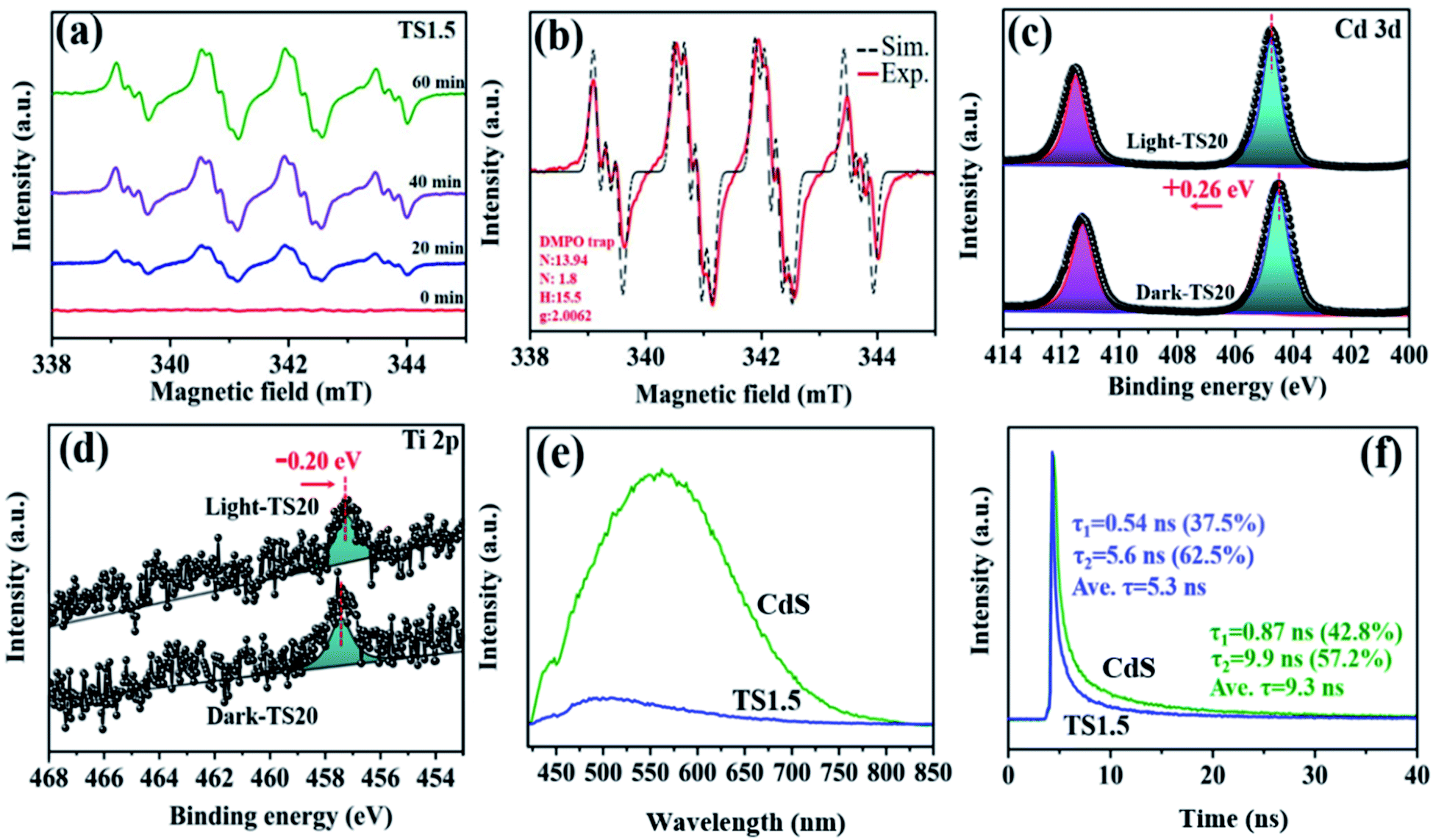 | ||
| Fig. 5 (a) In situ ESR spectra of TS1.5 monitored during the photocatalytic reaction with the increase of reaction time; (b) simulation results of the amine free-radical; XPS spectra of Cd 3d (c) and Ti 2p (d) in the TS1.5 sample under dark conditions and irradiation at 402 nm; PL emission (e) and time-resolved photoluminescence spectra (f) of TS1.5 and CdS samples. | ||
The photogenerated electron–hole transfer pathway between Ti3C2Tx and CdS was investigated by in situ XPS (Fig. S18, ESI†). As shown in Fig. 5c, under dark conditions, two peaks corresponding to Cd 3d5/2 (404.5 eV) and Cd 3d3/2 (411.3 eV) of TS20 are observed, which shift by 0.26 eV towards high binding energy under light irradiation, indicating a reduced electron cloud density around Cd 2p. Simultaneously, a slight negative shift (by 0.2 eV) in the Ti 2p binding energy over the TS20 composite under light irradiation is detected (Fig. 5d), indicating an increase in its electron density. The change in the binding energy illustrates that these electrons are decreased around both Cd and S while they increased for the Ti element under light irradiation, which is mainly due to the migration of photogenerated charges from CdS to the Ti3C2Tx cocatalyst.
Transient photocurrent responses of CdS and TS1.5 samples were further used to clarify the charge transfer ability under intermittent light irradiation. As shown in Fig. S19a (ESI†), the TS1.5 composite exhibits more than 4 times higher photocurrent intensity than the sample of CdS, indicating the enhanced charge transfer ability. To gain insight into the charge transfer efficiency between different samples, cyclic voltammetry (CV) curves over the different samples were recorded (Fig. S19b, ESI†). The results show that both the CdS and TS1.5 electrodes have similar redox peaks in the same range while the current density over TS1.5 is obviously larger than that of CdS, which is consistent with the observation in transient photocurrent measurements. This further illustrates the acceleration effect of Ti3C2Tx on facilitating the charge transfer process in the TS1.5 sample, thus promoting the photocatalytic activity toward H2 generation and imine production. Polarization curves were also recorded to investigate the overpotential for H2 evolution over the CdS and TS1.5 samples and the results are displayed in Fig. S19c (ESI†). The TS1.5 composite possesses a low overpotential and high current density as compared to the CdS sample, which indicates that the introduction of Ti3C2Tx can accelerate the H2 production kinetics, consequently, achieving the high H2 evolution activity. Both the enhanced charge transfer separation efficiency and the lowered H2 generation overpotential are favourable for achieving efficient photocatalytic performance over the TS1.5 catalyst, compared with many existing reports (Table S2 ESI†). Furthermore, the photoluminescence (PL) spectrum was recorded to investigate the annihilation and migration dynamics of photogenerated charge carriers. The electrons inside the semiconductor are excited, and then jump to an excited state after absorbing photons. When the excited electrons recombine with holes, the excess energy can be released through radiative and non-radiative decay. As observed in Fig. 5e, despite that the PL curves are similar, the PL intensity of TS1.5 is significantly diminished as compared with CdS, which is attributed to the introduction of Ti3C2Tx to inhibit the recombination of electrons and holes. Time-resolved photoluminescence (TRPL) spectroscopy was employed to reveal the lifetime of the charge carriers, as presented in Fig. 5f. The average emission lifetime of CdS is 9.3 ns, which is longer than that of TS1.5 (5.3 ns). This can be explained by the existence of more effective non-radiation attenuation pathways to transfer the photoexcited electrons from CdS to Ti3C2Tx, and then, shortening the lifetime of charge carriers. The above-mentioned results indicate that the hybridization of Ti3C2Tx and CdS can effectively enhance the kinetics of charge transfer and separation, thereby contributing to the improvement of dual-functional catalytic activity for the simultaneous H2 formation and benzylamine coupling reaction.
Based on the above discussion, a possible reaction mechanism for photocatalytic benzylamine oxidation integrated with H2 production over the TS1.5 composite was proposed (Scheme 1). Specifically, benzylamine and water molecules are adsorbed on the catalyst via N–H and H–O–H functional groups, respectively, to form TS1.5⋯N–H and TS1.5⋯H–O–H surface complexes and initiate the activation of the reactant molecules after reaching adsorption and desorption equilibrium. Under light irradiation, the photogenerated electrons could transfer efficiently from the conduction band (CB) of CdS to the Ti3C2Tx cocatalyst, leaving the holes in the valence band (VB) of CdS. The oxidation potential of the photogenerated holes in CdS (1.63 eV vs. NHE, Fig. S20a, ESI†) and Bi2MoO6 (2.28 eV vs. NHE, Fig. S21, ESI†) is more positive than that of benzylamine oxidation (0.76 eV vs. NHE). Therefore, the holes will induce the deprotonation of benzylamine to form amine free-radical intermediates, which are further oxidized to imine products by coupling with other benzylamine molecules and release protons. Simultaneously, the photogenerated electrons can produce H2 from protons dehydrogenated from benzylamine and through water splitting because of the favorable CB position of CdS (−0.72 eV vs. NHE, Fig. S20b, ESI†) and Bi2MoO6 (−0.32 eV vs. NHE, Fig. S21, ESI†). Then, the desorption of as-formed imine molecules and H2 molecules from the surface of the photocatalyst lead to accomplish the overall photocatalytic cycle. The overall photocatalytic reaction processes for simultaneous H2 production and benzylamine oxidation are displayed in Fig. S22 (ESI†).
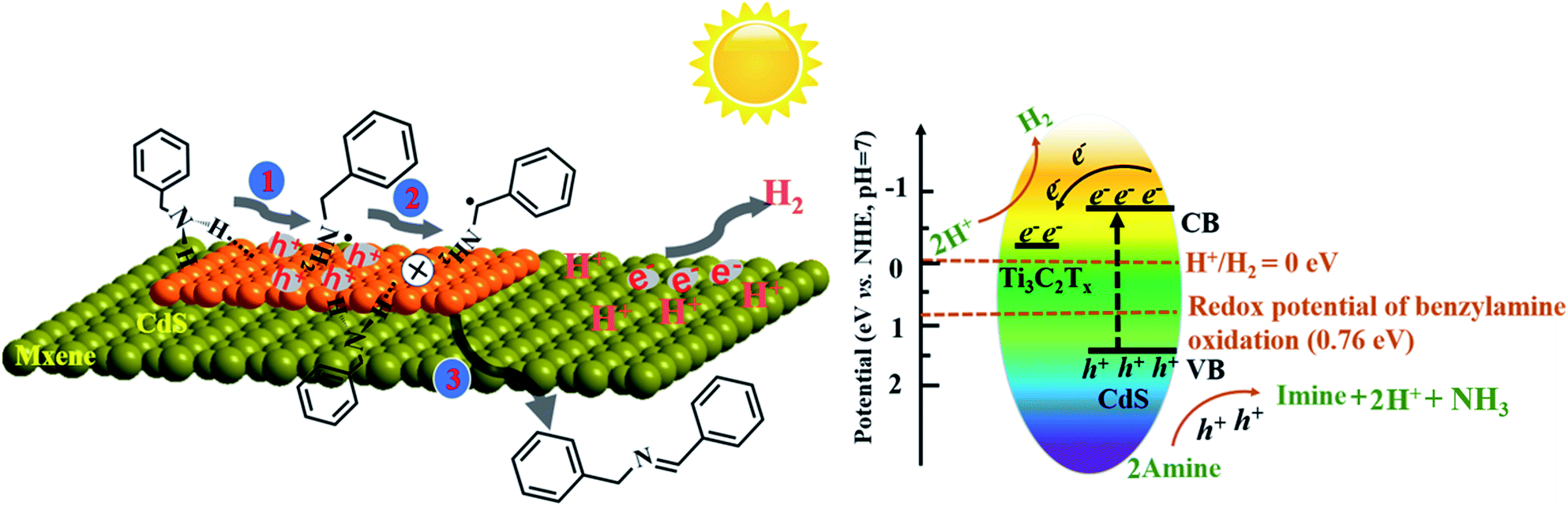 | ||
| Scheme 1 Proposed reaction mechanism for photocatalytic oxidative coupling of benzylamines to imines integrated with H2 production over the TS1.5 composite. | ||
Conclusions
In summary, we have successfully prepared ultrathin 2D/2D Ti3C2Tx/semiconductor (CdS and Bi2MoO6) hybrid photocatalysts for simultaneous H2 production and benzylamine oxidation under visible light irradiation. Both the Ti3C2Tx/CdS (TS) and Ti3C2Tx/Bi2MoO6 (TM) composites exhibit higher H2 and imine yield than the blank ones (i.e., CdS and Bi2MoO6). The photoactivity improvement over the Ti3C2Tx/semiconductor heterostructures has been systematically investigated. The in situ light irradiation XPS spectra and photoelectrochemical analysis reveal that the introduction of Ti3C2Tx could significantly accelerate the charge carrier transfer from the semiconductors to the Ti3C2Tx cocatalyst and reduce the recombination of photogenerated electron–hole pairs, thus promoting the photocatalytic performance. Moreover, the strong adsorption of benzylamine reactants and the easy desorption of imine products over the TS1.5 composites have been proved by in situ FTIR spectroscopy, which is favourable for the photocatalytic redox reactions. After evolution of the reaction intermediates via in situ ESR, a possible reaction mechanism for the photocatalytic benzylamine coupling reaction combined with H2 generation is proposed.Experimental
Reagents and chemicals
All reagents were analytical grade and used without further purification. Cadmium chloride (CdCl2), bismuth nitrate pentahydrate (Bi (NO3)3·5H2O), lithium fluoride (LiF), sodium molybdate dihydrate (Na2MoO4·2H2O) and hexadecyltrimethylammonium bromide (C19H42NBr) were purchased from Aladdin technology Co., Ltd. Sulfur sublimed was obtained from Damao chemical reagent (Tianjing) Co., Ltd. Titanium aluminum carbide (Ti3AlC2) was obtained from 11 technology (Beijing) Co., Ltd. Hydrochloric acid was purchased from Xilong scientific Co., Ltd.Synthesis of Ti3C2Tx
Ti3C2Tx nanosheets were synthesized referring to a previous report.48 In detail, Ti3C2Tx was prepared by etching layered Ti3AlC2 powder (2 g) in a mixed solution containing LiF (2 g) and HCl (9 M, 40 mL) and stirring for 24 h at 35 °C. The residue at the end of the reaction was washed by ultrasonication with ethanol (intercalation and stripping effect) and deionized water for 5 times, and then placed in a vacuum oven overnight at 25 °C. Finally, the black powder obtained is Ti3C2Tx nanosheets.Synthesis of Ti3C2Tx/Bi2MoO6
Ti3C2Tx/Bi2MoO6 nanosheets were synthesized referring to a previous report with some modifications.27 Bi (NO3)3·5H2O (2 mmol) and a certain amount of Ti3C2Tx nanosheets were added into 40 mL water and labelled as solution A. Na2MoO4·2H2O (1 mmol) and CTAB (0.1 g) were dissolved in 40 mL water and labelled as solution B. Afterwards, solution A was slowly transferred to solution B under continuous stirring. After 1 h, the mixture was transferred to a 100 mL autoclave and maintained at 120 °C for 24 h. The obtained precipitates were repeatedly washed with deionized water and anhydrous ethanol, and then dried at 60 °C overnight in a vacuum oven. The prepared Ti3C2Tx/Bi2MoO6 hybrids with different Ti3C2Tx loadings (0.5, 1, 1.5, 2 and 5 wt%) are denoted as TM0.5, TM1, TM1.5, TM2 and TM5. The synthesis procedure of Bi2MoO6 nanosheets was similar to the above steps, without the introduction of Ti3C2Tx nanosheets.Synthesis of Ti3C2Tx/CdS
Specifically, CdCl2 (0.75 mmol) was added to a mixture of diethylenetriamine and deionized water with a volume ratio of 3![[thin space (1/6-em)]](https://www.rsc.org/images/entities/char_2009.gif) :1 and stirred until completely dissolved. Subsequently, a certain amount of Ti3C2Tx was slowly added to the above mixture and stirred for 4 h to guarantee the dispersion of Cd2+ on the Ti3C2Tx nanosheet. S powder (4 mol) was added to the previous solution and stirred at room temperature for 1 h. Then, the mixture was transferred to a 100 mL autoclave and kept at 80 °C for 3 h. Finally, the as-fabricated samples were centrifuged, washed several times with deionized water and ethanol, and dried in a vacuum oven at 60 °C overnight. The mass fraction ratios of Ti3C2Tx in the Ti3C2Tx/CdS composites were 0.5%, 1%, 1.5%, 2% and 5%, and the prepared samples were labelled as TS0.5, TS1, TS1.5, TS2 and TS5, respectively. The preparation of CdS nanosheets is consistent with the above method, except for the lack of additional Ti3C2Tx nanosheets.
:1 and stirred until completely dissolved. Subsequently, a certain amount of Ti3C2Tx was slowly added to the above mixture and stirred for 4 h to guarantee the dispersion of Cd2+ on the Ti3C2Tx nanosheet. S powder (4 mol) was added to the previous solution and stirred at room temperature for 1 h. Then, the mixture was transferred to a 100 mL autoclave and kept at 80 °C for 3 h. Finally, the as-fabricated samples were centrifuged, washed several times with deionized water and ethanol, and dried in a vacuum oven at 60 °C overnight. The mass fraction ratios of Ti3C2Tx in the Ti3C2Tx/CdS composites were 0.5%, 1%, 1.5%, 2% and 5%, and the prepared samples were labelled as TS0.5, TS1, TS1.5, TS2 and TS5, respectively. The preparation of CdS nanosheets is consistent with the above method, except for the lack of additional Ti3C2Tx nanosheets.
Materials characterization
The zeta potentials of the catalysts were determined on a zetasizer (Nano ZS90, Malvern Instrument Ltd.) with deionized water as solvent (pH = 7). XRD measurement of the as prepared samples was performed on a D-max 2200 VPC (Japan) with a scanning speed of 5° min−1 (scanning range of 10–70°, λ = 0.15406 nm) using Cu Kα radiation. The microstructure and morphology of the samples were investigated by field scanning electron microscopy (FE-SEM) on a JSM-6330 F and spherical aberration-corrected scanning transmission electron microscopy (aberration-corrected STEM) on a JEM-ARM200P. The thickness information of the sample was obtained by atomic force microscopy (AFM; Agilent 5,500 AFM, Agilent Technologies, USA) in tapping mode. The light-absorption capacities of the samples were studied via UV-vis diffuse reflectance spectroscopy (UV-vis DRS, UV2450 spectrophotometer), and BaSO4 was used as a reference. The XPS and UPS of the samples were performed on an ESCALAB 250 spectrometer with a monochromatic Al Kα radiation source. The binding energy was corrected with reference to the C1s peak at 284.8 eV. The experimental parameters (excitation wavelength, slit width, and temperature) were consistent to ensure the comparability of PL spectra. Raman spectroscopy was carried out on a Nicolet NXR 9650 equipped with a 532 nm wavelength laser. Time-resolved photoluminescence (PL) measurements for samples were performed using an Edinburgh Instruments FLS920 spectrometer with an excitation and emission wavelength of 405 and 520 nm, respectively. The average decay time constants (τ) of the sample can be calculated through the following formula.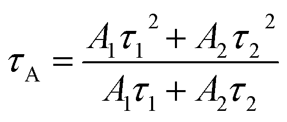
Photoelectrochemical measurements
Photoelectrochemical experiments were carried out in a three-electrode reaction cell using an electrochemical workstation (CHI660C, Chenhua Instrument, Shanghai, China). A Pt wire was employed as the counter electrode and Ag/AgCl was used as the reference electrode. The preparation of the working electrode was as follows: 10 mg of sample was dispersed in 2 mL of ethanol to obtain a suspension using ultrasound, and then the dispersed suspension was smeared on a clean FTO glass surface and dried for a whole night. The coated area of FTO glass was calculated to be 1 cm2. The photocurrent test was carried out in 0.5 M Na2SO4 solution with a 300 W Xe light source (λ ≥420 nm). The polarization curve test was performed in a 0.2 M Na2SO4 solution with a scan rate of 5 mV s−1. Cyclic voltammetry (CV) measurements were performed in 0.5 M Na2SO4 solution containing 0.01 M K3[Fe(CN)6]/K4[Fe(CN)6] (1:1) with a scan rate of 50 mV s−1.
In situ Fourier transform infrared spectroscopy (In situ FTIR)
In situ FTIR spectra of pyridine, imine and deuterium water adsorbed on catalysts were recorded on a Frontier spectrometer, and all spectra were normalized. 10 mg catalyst was pressed into a transparent sheet with a diameter of 1.5 cm and transferred to the sample holder, which could be moved along the in situ infrared tube. Then, the in situ infrared tube was sealed in a dynamic vacuum at 160 °C for 1 h to desorb the surface residue and then cooled to room temperature. 10 μL adsorbent (deuterium water, benzylamine, imine) was injected rapidly. After equilibrium of adsorption and desorption, the sample was measured by infrared spectroscopy to explore the physical and chemical adsorption and then further degassed at 120 °C for 1 h to explore the chemical adsorption of adsorbents on the samples.In situ electron paramagnetic resonance (In situ EPR)
In situ electron paramagnetic resonance (In situ EPR, JESFA-200, Japan) combined with spin-trapping technique was executed to investigate the free-radical species using 5,5-dimethyl-1-pyrroline-N-oxide (DMPO) as the trapping agent. 100 μL of the reaction solution was successively extracted through a syringe from the photocatalytic reaction, and then 10 μL of DMPO was added. The mixture was analysed by EPR under visible light irradiation. The test parameters for all samples were as follows: modulation width, 0.25 × 0.1 mT; microwave frequency, 9.30–9.50 GHz; power, 1.0 mW; modulation frequency, 100 kHz; and time constant, 0.03 s.In situ irradiated X-ray photoelectron spectroscopy (In situ XPS)
The chemical state of the fabricated sample was measured on an ESCALAB 250 before and after light irradiation. First, the sample was pressed into a separate disk (5 mg, 5 mm diameter), then the disk was placed into the sample holder which could be moved horizontally along the XPS chamber by a manipulator. Before the XPS measurements, the sample was treated under dynamic vacuum (8 × 10⁻⁹ Torr) for 12 h to remove surface contaminants and transferred to the analysis chamber to execute the in situ XPS measurements. Since the sample shows obvious visible light absorption, the 405 nm light was introduced into the sample holder of the XPS chamber and placed 2 cm away from the sample. Considering the excitation relaxation effect of electrons, the sample should be irradiated with light for 2 minutes before the test to achieve a balanced separation of electrons and holes.Photocatalytic measurements
Photocatalytic benzylamine oxidation integrated with H2 production was carried out in a Pyrex reaction tube equipped with a cooling system. A 300 W Xe lamp light source with a 420 nm filter was assembled as a light source system. In detail, the Pyrex reactor containing the catalyst (10 mg) was evacuated and then backfilled with Ar. The Pyrex reactor tube containing the catalyst was evacuated and then filled with Ar. Then, a mixture of degassed DMF (5 mL), water (2.5 mmol) and benzylamine (0.5 mmol) was injected into the reactor via a syringe under continuous stirring, and then the photocatalytic reaction was initiated under Xenon lamp irradiation. Isotope labelling experiments were performed using deuterium water instead of water while other conditions remained unchanged. In the detection process, helium gas was considered as a carrier gas to identify hydrogen and deuterium gas. As the gas thermal conductivity follows the rule: H2 > He > D2 deuterium gas showed a positive GC peak, while hydrogen gas showed a negative GC peak.Conflicts of interest
There are no conflicts to declare.Acknowledgements
This work was supported by the National Natural Science Foundation of China (No. 51972348, 21905313, 21938001, and 21961160741), the Key-Area Research and Development Program of Guangdong Province (2019B110206002), the Local Innovative and Research Teams Project of Guangdong Pearl River Talents Program (2017BT01C102), and the National key Research and Development Program Nanotechnology Specific Project (No. 2020YFA0210900).Notes and references
- Y. T. Zhang, L. J. Pei, Z. F. Zheng, Y. Yuan, T. F. Xie, J. Yang, S. Chen, J. W. Wang, E. Waclawikf and H. Y. Zhu, J. Mater. Chem. A, 2015, 3, 18045–18052 RSC.
- P. L. Wang, X. Y. Li, S. Y. Fan, Z. F. Yin, L. Wang, M. Tade and S. M. Liu, Nano Energy, 2021, 83, 105831 CrossRef CAS.
- H. Liu, C. Y. Xu, D. D. Li and H. L. Jiang, Angew. Chem., Int. Ed., 2018, 57, 5379–5383 CrossRef CAS PubMed.
- C. C. Zhao, Y. J. Gao, Z. Y. Zhang and D. Ma, Chin. J. Chem., 2020, 38, 1292–1298 CrossRef CAS.
- A. Santiago-Portillo, J. Blandez, S. Navalón, M. Álvaroa and H. García, Catal. Sci. Technol., 2017, 7, 1351 RSC.
- H. W. He, Z. Li, K. Li, G. Y. Lei, X. L. Guan, G. L. Zhang, F. B. Zhang, X. B. Fan, W. C. Peng and Y. Li, ACS Appl. Mater. Interfaces, 2019, 11, 31844–31850 CrossRef CAS PubMed.
- Z. Y. Zhang, C. C. Zhao, Y. S. Duan, C. Wang, Z. C. Zhao, H. J. Wang and Y. J. Gao, Appl. Surf. Sci., 2020, 527, 146693 CrossRef CAS.
- X. Y. Dong, H. M. Hao, N. N. Wang, H. Yuan and X. J. Lang, J. Colloid Interface Sci., 2021, 590, 387–395 CrossRef CAS PubMed.
- Y. H. Ren, J. h. Zou, K. Q. Jing, Y. Y. Liu, B. B. Guo, Y. J. Song, Y. Yu and L. Wu, J. Catal., 2019, 380, 123–131 CrossRef CAS.
- Z. Q. Liu, Q. Su, P. Y. Ju, X. D. Li, G. H. Li, Q. L. Wu and B. Yang, Chem. Commun., 2020, 56, 766–769 RSC.
- P. Chen, L. H. Meng, L. Chen, J. K. Guo, S. Shen, C. T. Au and S. F. Yin, ACS Sustainable Chem. Eng., 2019, 7(16), 14203–14209 CrossRef CAS.
- H. J. Chen, C. Liu, M. Wang, C. F. Zhang, N. C. Luo, Y. H. Wang, H. Abroshan, G. Li and F. Wang, ACS Catal., 2017, 7(5), 3632–3638 CrossRef CAS.
- W. k. Shang, Y. G. Li, H. W. Huang, F. L. Lai, M. Roeffaers and B. Weng, ACS Catal., 2021, 11, 4613–4632 CrossRef CAS.
- G. Q. Han, Y. H. Jin, R. Burgess, N. Dickenson, X. M. Cao and Y. J. Sun, J. Am. Chem. Soc., 2017, 139, 15584–15587 CrossRef CAS PubMed.
- Z. G. Chai, T. T. Zeng, Q. Li, L. Q. Lu, W. J. Xiao and D. Xu, J. Am. Chem. Soc., 2016, 138(32), 10128–10131 CrossRef CAS PubMed.
- J. Xiong, P. Song, J. Di, H. M. Lian and Z. Liu, J. Mater. Chem. A, 2019, 7, 25203–25226 RSC.
- C. L. Tan, X. H. Cao, X. J. Wu, Q. Y. He, J. Yang, X. Zhang, J. Z. Chen, W. Zhao, S. K. Han, G. Nam, M. Sindoro and H. Zhang, Chem. Rev., 2017, 117(9), 6225–6331 CrossRef CAS PubMed.
- C. K. Yao, A. Yuan, Z. S. Wang, H. Lei, L. Zhang, L. M. Guo and X. P. Dong, J. Mater. Chem. A, 2019, 7, 13071–13079 RSC.
- B. Weng, Q. Quan and Y.-J. Xu, J. Mater. Chem. A, 2016, 4, 18366–18377 RSC.
- S. G. Li, L. Q. Bai, N. Ji, S. X. Yu, S. Lin, N. Tian and H. H. Wei, J. Mater. Chem. A, 2020, 8, 9268–9277 RSC.
- Y. Huang, Y. Liu, D. Y. Zhu, Y. N. Xin and B. Zhang, J. Mater. Chem. A, 2016, 4, 13626–13635 RSC.
- L. Wang, Y. Zhang, L. Chen, H. X. Xu and Y. J. Xiong, Adv. Mater., 2018, 30, 1801955 CrossRef PubMed.
- L. Liang, F. C. Lei, S. Gao, Y. F. Sun, X. C. Jiao, J. Wu, S. Qamar and Y. Xie, Angew. Chem., Int. Ed., 2015, 54, 13971–13974 CrossRef CAS PubMed.
- C. B. Bie, J. W. Fu, B. Cheng and L. Y. Zhang, Appl. Surf. Sci., 2018, 462, 606–614 CrossRef CAS.
- S. Park, H. Song, C. W. Lee, S. W. Hwang and I. S. Cho, ACS Appl. Mater. Interfaces, 2015, 7, 21860–21867 CrossRef CAS PubMed.
- S. Hua, P. Z. Qiao, L. P. Zhang, B. J. Jiang, Y. T. Gao, F. Hou, B. G. Wu, Q. Lia, Y. Jiang, C. G. Tian, W. Zhou, G. H. Tian and H. G. Fu, Appl. Catal., B, 2018, 239, 317–323 CrossRef.
- S. W. Cao, B. J. Shen, T. Tong, J. W. Fu and J. G. Yu, Adv. Funct. Mater., 2018, 28, 1800136 CrossRef.
- J. D. Hu, D. Y. Chen, Z. Mo, N. J. Li, Q. F. Xu, H. Li, J. H. He, H. Xu and J. M. Lu, Angew. Chem., Int. Ed., 2019, 58, 2073–2077 CrossRef CAS PubMed.
- Y. L. Li, Y. L. Sun, T. F. Zheng, Y. Dall'Agnese, C. Dall'Agnese, X. Meng, S. Sasaki, H. Tamiaki and X. F. Wang, J. Mater. Chem. A, 2018, 6, 9124–9131 RSC.
- A. Shahzada, K. Rasoolb, M. Nawaza, W. Mirana, J. Janga, M. Moztahidaa, K. Mahmoud and D. Lee, Chem. Eng. J., 2018, 349, 748–755 CrossRef.
- S. X. Min, Y. Xue, F. Wang, Z. G. Zhang and H. T. Zhu, Chem. Commun., 2019, 55, 10631–10634 RSC.
- Y. j. Li, Y. Y. Liu, D. N. Xing, J. J. Wang, L. R. Zheng, Z. Y. Wang, P. Wang, Z. K. Zheng, H. F. Cheng, Y. Dai and B. B. Huang, Appl. Catal., B, 2021, 285, 119855 CrossRef CAS.
- C. Yang, Q. Y. Tan, Q. Lia, J. Zhou, J. J. Fand, B. Lie, J. Sun and K. L. Lv, Appl. Catal., B, 2020, 268, 118738 CrossRef CAS.
- L. Cheng, Y. C. Tang, M. Xie, Y. T. Sun and H. Liu, J. Alloys Compd., 2021, 864, 158913 CrossRef CAS.
- Y. Hu, L. Wang, T. R. Lin, N. Zhao, M. N. Shi, J. Peng, J. Q. Li, W. Q. Shi and M. L. Zhai, Adv. Mater. Interfaces, 2020, 7, 1901839 CrossRef CAS.
- Y. L. Yang, D. N. Zhang and Q. J. Xiang, Nanoscale, 2019, 11, 18797–18805 RSC.
- B. J. Jin, Z. B. Jiao and Y. P. Bi, J. Mater. Chem. A, 2015, 3, 19702–19705 RSC.
- H. Wang, Y. Q. Wang, C. L. Jiang, K. H. Ye, X. H. He, C. Xue, Z. J. Yang, X. T. Zhou and H. B. Ji, ACS Appl. Mater. Interfaces, 2020, 12(2), 2259–2268 CrossRef CAS PubMed.
- Y. Huang, C. B. Liu, M. Y. Li, H. Z. Li, Y. W. Li, R. Su and B. Zhang, ACS Catal., 2020, 10, 3904–3910 CrossRef CAS.
- Y. C. Huang, K. S. Li, S. Q. Li, Y. Lin, H. Liu and Y. X. Tong, ChemistrySelect, 2018, 3, 7423–7428 CrossRef CAS.
- Y. Zheng, T. F. Zhou, X. D. Zhao, W. K. Pang, H. Gao, S. Li, Z. Zhou, H. k. Liu and Z. P. Guo, Adv. Mater., 2017, 29, 1700396–1700404 CrossRef PubMed.
- T. Cai, L. L. Wang, Y. T. Liu, S. Q. Zhang, W. Y. Dong, H. Chen, X. Y. Yi, J. L. Yuan, X. N. Xia, C. B. Liu and S. L. Luo, Appl. Catal., B, 2018, 239, 545–554 CrossRef CAS.
- K. Hadjiivanov, H. Knözinger, B. Tsyntsarski and L. Dimitrov, Catal. Lett., 1999, 62, 35–40 CrossRef CAS.
- P. Gupta, A. C. Dillon, A. S. Bracker and S. M. George, Surf. Sci., 1991, 245, 360–372 CrossRef CAS.
- A. Sadat and I. Joye, Appl. Sci., 2020, 10, 5918 CrossRef CAS.
- J. Ke, Y. L. Tang, H. Yi, Y. L. Li, Y. D. Cheng, C. Liu and A. W. Lei, Angew. Chem., Int. Ed., 2015, 54, 6604–6607 CrossRef CAS PubMed.
- W. Zou, X. H. Liu, C. Xue, X. T. Zhou, H. Y. Yu, P. Fan and H. B. Ji, Appl. Catal., B, 2021, 285, 119863 CrossRef CAS.
- B. B. Shao, J. J. Wang, Z. F. Liu, G. M. Zeng, L. Tang, Q. H. Liang, Q. Y. He, T. Wu, Y. Liu and X. Z. Yuan, J. Mater. Chem. A, 2020, 8, 5171 RSC.
Footnote |
| † Electronic supplementary information (ESI) available. See DOI: 10.1039/d1ta03573h |
| This journal is © The Royal Society of Chemistry 2021 |