
 Open Access Article
 This Open Access Article is licensed under a Creative Commons Attribution-Non Commercial 3.0 Unported Licence
High performance LATP thin film electrolytes for all-solid-state microbattery applications†
Valerie
Siller
 a,
Alex
Morata
*a,
Marc Nuñez
Eroles
a,
Raul
Arenal
bcd,
Juan Carlos
Gonzalez-Rosillo
a,
Juan Miguel
López del Amo
e and
Albert
Tarancón
*af
a,
Alex
Morata
*a,
Marc Nuñez
Eroles
a,
Raul
Arenal
bcd,
Juan Carlos
Gonzalez-Rosillo
a,
Juan Miguel
López del Amo
e and
Albert
Tarancón
*af
aCatalonia Institute for Energy Research (IREC), Jardins de les Dones de Negre 1, Planta 2, Sant Adrià del Besòs, Barcelona 08930, Spain. E-mail: atarancon@irec.cat; amorata@irec.cat
bInstituto de Nanociencia y Materiales de Aragon (INMA), CSIC-Universidad de Zaragoza, Calle Pedro Cerbuna, 50009 Zaragoza, Spain
cLaboratorio de Microscopias Avanzadas (LMA), Universidad de Zaragoza, Calle Mariano Esquillor, 50018 Zaragoza, Spain
dFundacion ARAID, 50018 Zaragoza, Spain
eCentre for Cooperative Research on Alternative Energies (CIC energiGUNE), Basque Research and Technology Alliance (BRTA), Alava Technology Park, Albert Einstein 48, 01510 Vitoria-Gasteiz, Spain
fCatalan Institution for Research and Advanced Studies (ICREA), Passeig Lluís Companys 23, Barcelona 08010, Spain
First published on 12th July 2021
Abstract
The NASICON superionic solid electrolyte Li1+xAlxTi2−x(PO4)3 (LATP) with 0.3 ≤ x ≤ 0.5 remains one of the most promising solid electrolytes thanks to its good ionic conductivity and outstanding stability in ambient air. Despite the intensive research for bulk systems, there are only very few studies of LATP in a thin film form (thickness < 1 μm) and its implementation in all-solid-state batteries and microbatteries. The following study fills this gap by exploring the properties of high performance LATP thin films fabricated by large-area Pulsed Laser Deposition (PLD). The as-deposited thin films exhibit an ionic conductivity of around 0.5 μS cm−1 at room temperature (comparable to the state-of-the-art of LiPON) which increases to a remarkably high value of 0.1 mS cm−1 after an additional annealing at 800 °C. A possible cause for this significant enhancement in ionic conductivity by two orders of magnitude is the formation of a glassy, intergranular phase. The performance of both as-deposited and annealed LATP films makes them suitable as solid electrolytes, which opens the path to a new family of stable and high performance all-solid-state thin film batteries.
Introduction
Electrochemical storage devices have experienced a fast proliferation over a broad variety of applications including transportation and portable electronics, dominating the research in this field over the past few decades. As a matter of fact, energy storage represents a main constraint for the full development of the constantly rising capabilities and demands for sustainable energy, electric vehicles and electronic devices, such as tablets and smart phones. Major requirements for those technologies are application dependent, but all share the necessity for high power densities and capacities, high peak currents, a long term stability together with increased safety and environmental friendliness.1 While storage on a larger scale will play a key role in the future mobility, as well as in domestic and industrial power supplies, the use of miniaturized devices is going to face an exponential growth, mainly boosted by the so-called Internet of Things (IoT). Billions of portable micro-devices, such as autonomous micro-electromechanical systems (MEMSs), wireless micro-sensors and transceivers, or implantable health monitoring devices will require proper power supplies.2–4 All-solid-state miniaturized batteries and supercapacitors with a compact shape and light weight are therefore essential for enabling high energy densities along with high stability and safety, as the hazards and physicochemical limitations of liquid electrolytes can be eliminated by utilizing solid electrolytes.2,5,6 The realization of all-solid-state batteries to replace common Li-ion batteries based on liquid electrolytes is still dependent on the development of feasible solid electrolyte materials of high ionic conductivity (10−5 to 10−3 S cm−1) near room temperature.7–9 LiPON usually is the material of choice in thin film solid electrolytes.9 Although it lacks fast ionic transport at room temperature (10−6 S cm−1), as a thin film of less than 1 μm thickness it can reach an area specific resistance (ASR) of 10 Ω cm2 and below.5,10 Unfortunately its purely amorphous nature reduces its stability when exposed to high temperatures, limiting its implementation in devices fabricated or operating at high temperatures.11,12 In contrast, crystalline electrolytes can withstand much higher temperatures and overcome these limitations.5Among the strongest candidates to replace LiPON thin film technologies, Li garnets are attracting worldwide interest.13 Only very recently, Li-garnet films have achieved competitive values of ∼10−4 to 10−5 S cm−1, attributed to the stabilization of the fast-conducting cubic phase by adding extra lithium during physical vapor deposition, by either Li3N14 or Li2O15 layers. However, the extreme sensitivity of the films upon exposure to ambient conditions has hindered its device integration. In contrast, other materials, such as LISICON or NASICON compounds, have received a lot of attention thanks to their high environmental and electrochemical stability and ionic conductivity, which can reach values as high as 10−2 to 10−3 S cm−1.5 The NASICON structure in particular attracts much interest, as it may serve as a solid electrolyte or potential electrode material upon its high adaptability in material composition, providing chemically and thermally stable materials of low electronic conductivity.16,17 Fast ionic conduction is enabled by differently coordinated Li occupation sites forming a three-dimensional network of mobility channels,18,19 leading to lithium diffusion coefficients as high as 1.4 × 10⁻¹¹ and 1.2 × 10⁻⁹ m2 s−1.20 The ionic conductivity is determined by the areal size of vacant triangles (formed by oxygen atoms between corner-sharing MO6 octahedra and XO4 tetrahedra), constituting the “bottlenecks” in the conduction channels responsible for charge transfer limitations in the bulk. With the partial replacement of tetravalent M2−x transition-metal ions with trivalent  cations, the “bottlenecks” can be broadened and the connecting oxygen ions are differently polarized, both acting as a possible source for accelerating ionic conduction for the interstitial ions.21 In LiTi2(PO4)3 the partial replacement of Ti4+ with Al3+ leads to a notable increase in ionic conductivity up to 10−4 S cm−1 and electronic conductivities as low as 10−10 S cm−1 at room temperature, therefore defining Li1+xAlxTi2−x(PO4)3 (LATP) as a feasible solid electrolyte for all-solid state batteries.22,23
Of more general importance is the problem of the multiple interfacial contact resistances evolving from grain boundaries within each of the cell components and at the solid–solid interface between the electrodes and the electrolyte.24,25 In this respect, physical vapor deposition techniques can offer a good control of the layer properties, unbeaten so far by any other thin film deposition technology, while still providing industrial up-scaling capabilities.9 Among them, Pulsed Laser Deposition (PLD) has become a popular choice to produce dense and highly oriented thin films (<1 μm) of high quality, uniformity and smooth surfaces, offering better stoichiometric transfer than sputtering from a variety of applicable target materials.26,27 Its high potential to resolve interfacial issues at the electrode–electrolyte interface, dominating the overall electrochemical performance of all-solid-state batteries, has been predicted as a relevant technology in commercialized thin film microbattery fabrication for more than a decade by Xia et al.28 and it is established as a well-suited deposition technique for a broad range of battery materials.9,29 Furthermore, we use a scalable Large Area (LA) PLD setup allowing depositions up to 4′′ wafers. NASICON-type AxM2(XO4)3 glass ceramics for the deposition in PLD have been first realized for sodium rechargeable battery systems with Na+ occupied A-sites.30 While past studies have explored Li-based NASICON thin films through a variety of deposition techniques,9,31–34 only very recently the first layers of Li1+xAlxTi2−x(PO4)3 were fabricated by PLD, although electrochemical performance was not presented.35
Despite the thorough structural characterization conducted in the aforementioned work and the excellent ionic conductivities reported for sputtered amorphous LATP films,32 the electrochemical performance of partially crystalline LATP thin film electrolytes and the role of grain boundaries and their local environment in the ionic conduction of such films have never been reported so far. Herein we demonstrate for the first time LA-PLD to form thin and dense NASICON based films of Li1+xAlxTi2−x(PO4)3 of around 500 nm and propose strategies to increase the performance of the as-deposited films by a factor of 100, reaching conductivity values up to 0.1 mS cm−1. The proposed procedure is based on lattice rearrangement and partial amorphization by controlling post-annealing conditions.
Experimental section
A dense pellet working as a PLD target has been fabricated by solid-state reactions. Prior to the reaction, the precursors Li2CO3 (99.997% Sigma Aldrich), Al2O3 (99.999% Sigma Aldrich), TiO2 (99.999% Sigma Aldrich) and NH4H2PO4 (99.999% Sigma Aldrich) were first dried to remove moisture and then weighed in a stoichiometric ratio to obtain x = 0.5 for Li1+xAlxTi2−x(PO4)3, including an excess of 10 wt% Li2CO3 to balance eventual Li loss during heat treatments. After thorough mixing and grinding in a mortar, the powder was milled with zirconia balls and slowly calcined at 650 °C and at 900 °C, with repeated grinding and milling steps in-between. The reacted powder was cold-pressed into a pellet of 3′′ diameter and finally sintered at 1000 °C.Thin films were deposited using a LA-PLD-5000 system from PVD products using a Coherent (Lambda Physik) COMPex PRO 205 KrF excimer laser (wavelength λ = 248 nm, pulse duration 20 ns, maximum pulse energy of 700 mJ, and maximum repetition rate f = 50 Hz). The partial oxygen pressure pO2 was fixed at 80 mTorr with a 5 sccm oxygen flow and a substrate temperature of 700 °C. Depositions were carried out under constant rotation of the target and substrate, with a fixed distance of 90 mm between them. The average laser fluence was set to 1.4 J cm−2. The fabricated layers were 440 ± 20 nm thick without significant changes after annealing (Fig. S14†). Post-annealing was carried out in a conventional Hobersal TR-25MFF furnace in ambient air, reaching temperatures between 700 and 900 °C under ramping of 1–3 °C min−1 and a subsequent dwelling of 5–10 h.
Different substrates (with the lateral dimensions of 1 × 1 cm) have been applied according to the needs of the different characterization methods carried out on the films. For the collection of SEM images, X-ray diffraction, STEM analysis and in-plane electrochemical impedance spectra the substrates consisted of chips cut from a (100) Si-wafer covered on both sides in 100 nm SiO2 and 300 nm Si3N4. For electronic cross-plane measurements and for improving the Raman signal of the thin films, Si3N4|SiO2|Si-wafers were covered with a thin sputtered Pt layer of 80 nm, with 10 nm Ti as an adhesive intermediate layer in-between. In order to conduct solid state NMR analysis, the LATP thin films were deposited on glassy SiO2 substrates. Deposition and annealing conditions were kept the same for all substrates. Further details about the characterization on different substrates can be found in the ESI.†
Scanning electron microscope images were collected using a ZEISS AURIGA equipped with a 30 kV Gemini FESEM column, an energy dispersive spectroscope (EDS) and an InLens detector. Topographic images were taken with a XE15-AFM from Park Systems, operating in tapping mode with a non-contact micro-cantilever of type OMCL-AC160TS from Olympus at a frequency of 292.21 kHz. Further structural analysis was performed by using an XRD Bruker-D8 Advance equipment utilizing Cu-Kα radiation (λ = 1.54184 Å), a Ni filter and a Lynx Eye detector. For better resolution of the most intense characteristic peaks resulting from the LATP lattice at lower angles, the measurements were conducted in a 2θ range of 18–32° with a step size of 0.01°. Additional diffractograms specialized in the analysis of thin films were obtained using a grazing incidence (GI) X-ray diffractometer with an incident angle ω of the beam between 0.33° and 0.40° at the Scientific and Technological Center (CCiT) at the University of Barcelona. Raman spectra were collected using a HORIBA Scientific iHR320 monochromator equipped with a HORIBA Syncerity CCD (1024 × 256, pixel size 26 μm × 26 μm) and a laser at λ = 532 nm (green), providing a spectral range between 100 and 7700 cm−1 (gratings available are 600, 1200 and 1800 lines per mm).
MAS-NMR measurements were performed using a Bruker Avance III 500 MHz (11.7 T) spectrometer operating at Larmor frequencies of 500.24, 194.41 and 130.35 MHz for 1H, 7Li and 27Al respectively. Thin films of LATP deposited by LA-PLD on SiO2 glass substrates were employed in this experiment to avoid the complexity of multi-layered Si|SiO2|Si3N4 substrates. Both the as-deposited and annealed films at 800 °C for 5 h were ground to powders and packed in 2.5 mm rotors. These films showed the same structural and electrochemical features as those deposited on Si3N4. The MAS frequency was set to 20 kHz for all measurements. References for the 7Li and 27Al spectra consisted of 0.1 M LiCl and Al(NO3)3. Single pulses were applied in all cases with non-selective π/2 pulse durations of 2.3 μs for 27Al and 2.4 μs for 7Li. DMFIT software was used to reconstruct and simulate the spectra.
Thin film lamellae (40–50 nm thickness) of the as-deposited and annealed LATP thin films on Si3N4 covered substrates were prepared across-plane with a Ga-ion FIB (FEI Dual Beam Helios NanoLab 600). STEM experiments were carried out using a probe aberration corrected Titan (Thermo Fisher Scientific) equipped with a high-brightness field emission gun operating at 300 keV. Additional EDS and EELS have been conducted using the STEM mode (spectrum-imaging acquisition37), minimizing possible damage to the material structure by the electron beam.
In order to determine the LATP thin film ionic conductivity and activation energy, temperature dependent electrochemical impedance spectra were collected using a Linkam LTS600 probe station performing in-plane and cross-plane measurements. Rectangular, parallel gold electrodes for in-plane measurements have been sputtered with a shadowmask at IREC facilities. Circular gold micro-electrodes of 300 μm diameter and a 10 nm thin adhesive layer of Ti have been fabricated using lithographic techniques at the Institute of Microelectronics of Barcelona IMB-CNM, in order to perform electronic cross-plane measurements. Gold electrodes have been connected through two tungsten tips in a pseudo-four-probe configuration, eliminating the resistance of the measurement wires. AC measurements were controlled with a Novocontrol Alpha-A impedance spectrometer with a ZG4 electrochemical interface and collected in a frequency range of 40 MHz to 100 mHz and a perturbation voltage of 100 mV with zero bias. All conductivity experiments were performed in a dry gas mixture of 79% N2 and 21% O2, with maximum temperatures below 500 °C, in order to limit material degradation and probe station contamination.38 In order to exclude the influence of surrounding humidity, all measurements were collected by ramping down from high to low temperatures. The final fitting of the impedance spectra was carried out using ZView software with suitable equivalent circuits.
Results and discussion
The structure and composition of the target have been confirmed to exhibit LiTi2(PO4)3 in the NASICON phase, based on the analysis performed with XRD and Raman spectroscopy (see ESI Fig. S1 and S2†), indicating AlPO4 as the common secondary phase appearing after increased sintering temperatures.39 A slight peak shift of the LTP pattern in X-ray diffractograms towards higher 2θ angles indicates the intercalation of the Al dopant, forming Li1+xAlxTi2−x(PO4)3 with 0.3 ≤ x ≤ 0.5. For the LA-PLD depositions of the films, first we optimized the oxygen partial pressure during deposition and found that a stoichiometric composition of the as-deposited layers is achieved at 80 mTorr (Fig. S3†). Second, a thorough study of the ionic conductivity of the films as a function of the annealing temperature and dwell time was carried out, resulting in conductivities as high as 0.1 mS cm−1 under the optimal conditions through a highly reproducible and robust procedure (discussed in detail in the last section of this manuscript and in the ESI†). Following this reasoning, we exemplify next the key factors governing the 100 times increase in the ionic conductivities between the best annealed films and their as-deposited counterparts. Thin films have been studied as-deposited (AD) at 700 °C and post-annealed (A) at 800 °C for 5 h in ambient air, using silicon single-crystalline chips with Si3N4 as the amorphous top layer, and glassy SiO2 or Pt-covered Si-substrates, with a great stability at elevated temperatures. The resulting microstructure was studied by STEM and compared with images collected in SEM (Fig. 1).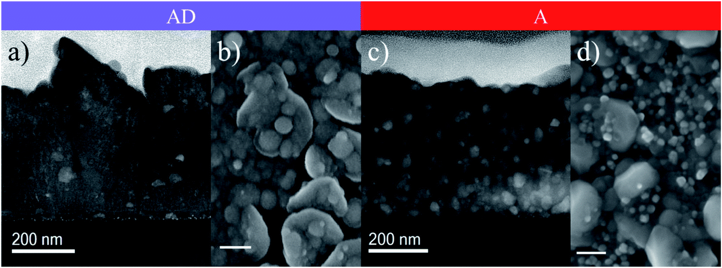 | ||
| Fig. 1 STEM dark field images collected for the as-deposited (a) and annealed (c) thin films in the cross section of the layers with a thickness around 445 nm. SEM images from the surface of the same layers AD in (b) and A in (d). The white bar at the bottom lower left equals 200 nm. | ||
The microstructure of the AD layer appears rugged on its surface but locally compact across the layer, mainly consisting of very fine nano-crystallites embedded in larger particles (Fig. 1a and b) with a surface roughness of Rq ∼ 30 ± 5 nm, as shown by the corresponding AFM image (Fig. S4a†). After annealing, small particles are approximately homogeneously distributed within a dense matrix with a more compact surface (Fig. 1c and d) and a similar morphology with Rq ∼ 26 ± 6 nm (Fig. S4b†). The crystal structure of both as-deposited and annealed thin films is confirmed to be LATP with only small amounts of secondary phases visible by means of XRD and Raman spectroscopy, as shown in Fig. 2.
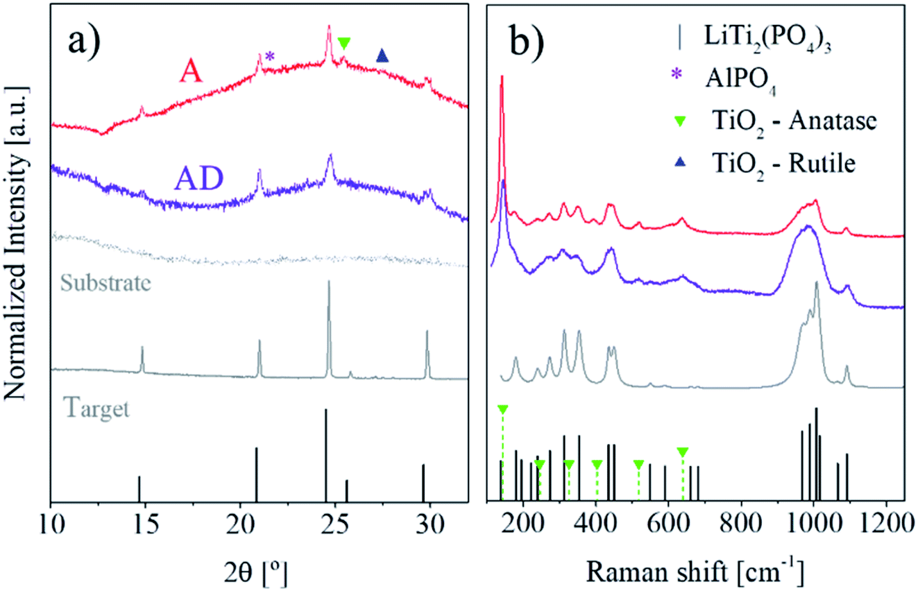 | ||
| Fig. 2 Structural analysis of LATP for AD and A thin films with respect to the target signal (a) by XRD and (b) by Raman spectroscopy. References for XRD correspond to Li2Ti(PO4)3 (JCPDS 00-035-0754), AlPO4 (JCPDS 01-072-1161), anatase (JCPDS 01-073-1764) and rutile (JCPDS 01-078-1510), as well as Raman spectra with corresponding LTP21 and anatase40 (b) for equivalent layers deposited on Pt (compare to the signal on Si3N4 substrates in Fig. S5a†). | ||
Upon annealing, diffraction peaks become sharper, indicating the growth of crystallites in the layer, in accordance with the STEM images in Fig. 1a and c. Some impurities appear to be present especially after annealing, as shown by the small peak at 21.6° indicating the presence of AlPO.4 GI-XRD revealed additional crystalline impurities, mostly consisting of rutile TiO2 (see Fig. S6b†). Raman spectra (Fig. 2b) confirm the presence of the anatase TiO2 phase (strongest visible vibrational mode at 140 cm−1), for both as-deposited and annealed samples, with a notable increase in the relative intensity for the latter. The increased intensity of the XRD peak at 25.4° is compatible with the appearance of anatase TiO2, although this point cannot be confirmed as it is overlapping with the (113) peak of LATP. The appearance of these minor secondary phases is in concordance with the literature, in which the formation of TiO2 is reported as a result of lithium loss during the annealing at elevated temperatures above 750 °C.35 Also, it was reported that the lattice transformation of rhombohedral LATP to orthorhombic AlPO4 upon the suspension of Ti appears at all temperatures above 500 °C with an increasing fraction for higher and longer temperature treatments.38,41 However, it is important to remark that for our films the appearance of TiO2 correlates with the formation of AlPO4, as both are detected in the annealed films. The broad scattering hump present in the background signal of the X-ray diffractograms in Fig. 2a results most likely from the amorphous Si3N4 substrates. However, GI-XRD (Fig. S6b†) could not unambiguously determine the presence or absence of amorphous phases, especially in the surroundings of the LATP crystallites.
We now take advantage of high-resolution spectroscopy techniques to understand the local environment of Al- and Li-site occupation and their coordination in the lattice. Solid state NMR was performed on glassy SiO2 substrates for as-deposited and annealed thin films and spectra are shown in Fig. 3 for the 27Al and 7Li chemical shifts. The spectrum of 27Al-MAS-NMR recorded for the as-deposited layers in Fig. 3a consists of a non-resolved, broad contribution in the range of δ ≈ −40 to 60 ppm, in accordance with the previously reported coordination environments of AlOy in the literature.42 As is common for LATP in the NASICON structure, one would expect a chemical shift δ at −15 ppm to appear for aluminum in the octahedral coordination forming AlO6, but instead a predominant chemical shift for AD appears at δ ≈ 15 ppm, ascribed to five-coordinated AlO5 and related to an amorphous environment.18,43–45 In addition the signal resolved at δ ≈ 40 ppm can be ascribed to the tetrahedral coordination of AlO4 in the AlPO4 secondary phase, which exhibits a strong increase after annealing of 20% proportionally to the full 27Al-MAS-NMR spectrum. A crystalline phase of AlPO4 might appear as a result of lithium loss upon annealing, matching previous observations from XRD. In addition, the intensity of the peak at δ ≈ 40 ppm and the broadness of the Al signal in Fig. 3a support the idea of amorphous AlPO4 phases being locally present in the annealed layers.38
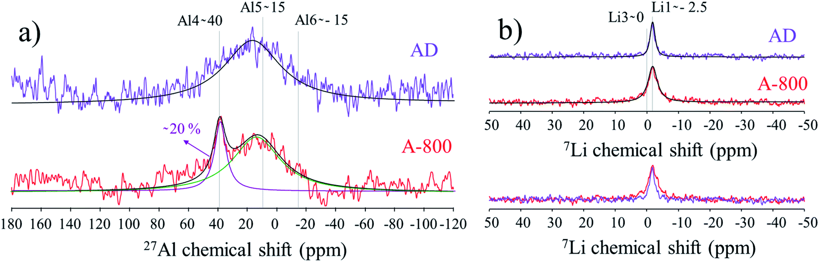 | ||
| Fig. 3 Solid state NMR spectra from as-deposited and annealed thin films on SiO2 substrates with the chemical shifts observed from (a) 27Al-MAS-NMR and (b) 7Li-MAS-NMR. Experimental curves have been fit (black lines) and possible assignments are indicated by vertical lines for the purpose of illustration. | ||
With respect to the 7Li spectra (Fig. 3b), the main peak at δ ≈ −2.5 ppm in the as-deposited films can be attributed to the preferable occupation of Li ions at the six-fold coordinated Li1 sites in the NASICON structure of LTP with good Li-ion mobility.36 After annealing the 7Li signal appears slightly broadened with a full width at half maximum of 3.9 ppm vs. 1.9 ppm for the as-deposited. This is consistent with lithium displacement in phases different from NASICON compounds (e.g. phases enriched with Li and P) and an increased amount of material amorphization.18,36,44 A second 7Li signal at δ ≈ 0 ppm usually appears for occupied Li3 sites as an indication for the incorporation of Al in the LATP structure.19,45 We hypothesize that the absence of such a sharp peak here could support the idea of amorphous Al-rich phases being present in the films. Local disorder in the LATP cannot be fully excluded, although we judge this scenario as unlikely due to the sharper LATP peaks observed in the XRD and Raman patterns of the annealed films.
Next, we performed HR-STEM dark field imaging and EELS mapping to understand the local chemical distribution. The AD films present initially a homogeneous distribution of elements, with titania (Fig. 4a and b) particles or grains embedded in a remarkably dense matrix of LATP. This is consistent with our previous observations from XRD and Raman, where the main peaks and bands detected correspond to LATP with only minor phases of TiO2. The strong rearrangement in elemental distribution upon annealing (Fig. 4c) shows a segregation between particles and their surrounding intergranular matrix. Different mechanisms appear to dominate the redistribution. First, Al-rich areas appear to be proportionate with the Ti intensities for the majority of the observable area. This relatively high concentration of Ti and Al inside the particles is attributed to the presence of LATP. A clear enrichment of Li outside the crystalline particles can be assigned to the sufficient intercalation of both Li and Al dopants inside the NASICON lattice. Hence, the remaining Li is enriched outside the particles, i.e., at the intergranular domains, ensuring good Li+ mobility across the film.
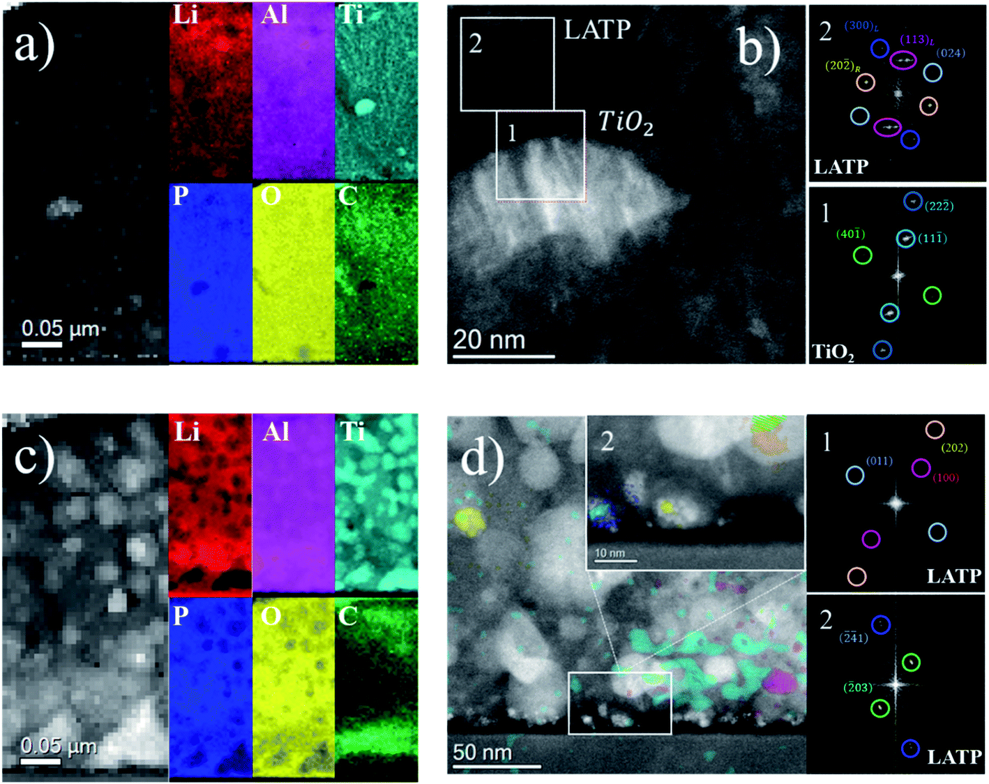 | ||
| Fig. 4 STEM dark field images of the thin films (a) AD and (c) A, with their corresponding EELS elemental maps. The HAADF-HRSTEM image in (b) for the AD layer shows a crystalline TiO2 particle embedded in the polycrystalline LATP matrix, followed by the corresponding FFTs of the marked regions-of-interest (1 and 2). In (d) the HAADF-HRSTEM image of A is shown with LATP crystalline particles embedded in an amorphous matrix, supported by the corresponding FFT of (1) the full frame image and (2) the magnification of the marked area of interest at the bottom of the layer with the corresponding LATP indexed planes. The only crystalline signals appearing in the FFT are colored (circular shapes) in the displayed HAADF-HRSTEM image. | ||
A closer look at the annealed samples by HR-STEM (Fig. 4d and S7†) reveals that crystalline particles are embedded (colored regions corresponding to the colored circles and the related indexed planes) with reflections in the FFT corresponding to interplanar distances for LATP crystallites, evidencing their high crystallinity. It is worth mentioning that only the colored regions showed some crystalline signal. In this sense, the weak amorphous signal of the intergranular matrix (perhaps more evident in Fig. S7e†) is masked by the high crystallinity of the embedded particles. Consequently Fig. 4c and d conclude that the grains primarily consist of LATP in a crystalline phase, with small amounts of crystalline LTP and an intergranular glassy phase being present, enriched in Li, P and O, consistent with the EELS elemental maps.
The compositional character of the amorphous matrix has been previously investigated in bulk materials, where excess in phosphorus drives to the formation of Li3PO4 and P2O5, or even LiTiPO5, acting as the sintering aid and therefore improving densification and the contact area between domains of different orientations.46,47 In the films presented in this work, the clear signal of Al also in the glassy phase might indicate that even amorphous AlPO4 can be partially present.38 The appearance of glassy phases around crystallites has been reported already in the first studies by Aono et al. on the replacement of Ti4+ with trivalent M3+ cations in the Li1+xMxTi2−x(PO4)3 matrix. Hence, secondary phases segregate near the grain boundary of surplus elements, leading to a better densification of the material and an improved ionic conductivity. This mechanism is frequently observed in bulk materials, but has not been reported to such an extent in thin films. In summary, we were able to identify a complex nanometric landscape of minor secondary phases (e.g. titania) coexisting with the main crystallites of LATP embedded in an intergranular glassy matrix enriched by Li, P and O and some Al upon annealing at 800 °C. Extensive modeling tools as the ones recently proposed for LiPON48,49 are required to fully understand the nature of the intergranular glassy phase. It is worth mentioning that similar phenomenology has been observed in Al-doped LLZO films, where Al was suggested to play a triple role as a sintering agent (decreasing crystallization temperature) and as a stabilizer of the highly conducting cubic phase and appears accumulated in amorphous domains at the grain boundaries.50 In the LISICON family, recent reports have also suggested the presence of nanocrystals in an amorphous matrix under certain conditions.51 Amorphization has also been studied in this family as a strategy to improve ionic conductivity.52
The ionic conductivity of the fabricated LATP thin films was evaluated at different temperatures by means of EIS. Fig. 5 shows the Nyquist plots collected in-plane for a layer as-deposited and annealed (a), with the corresponding Arrhenius plot for in-plane and across-plane conductivity measurements (b). The insets in (a) show the equivalent circuit (top inset, see the ESI† for detailed explanation) as a model for the fitting procedure and the corresponding measurement setup (central inset below, see Fig. S8a† for further description).
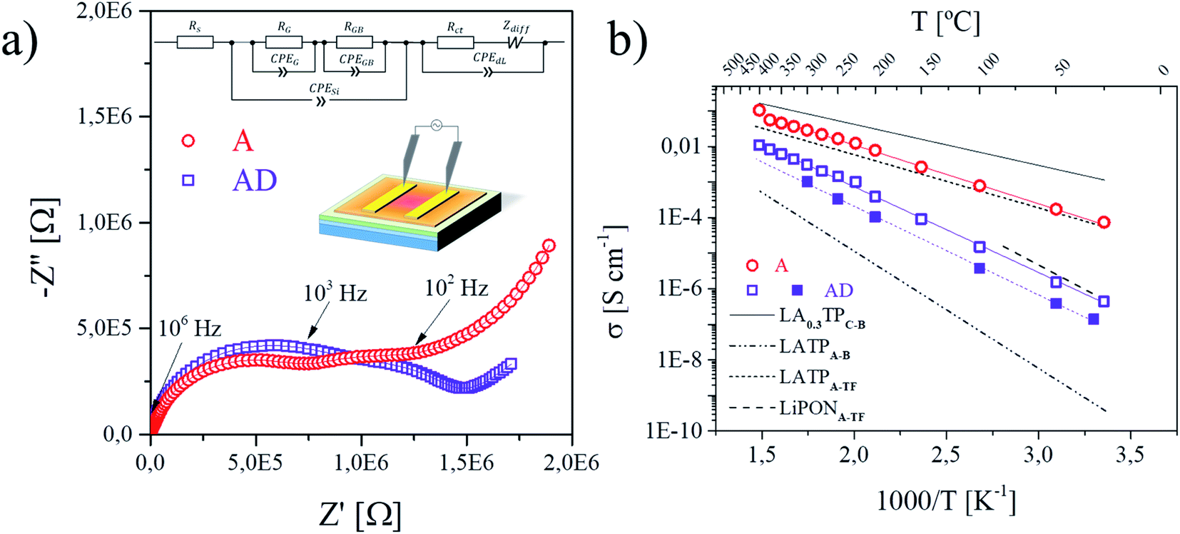 | ||
| Fig. 5 Data (symbols) and fitting (lines) of representative Nyquist plots are shown in (a) with the schematic in-plane measurement setup (center) and equivalent circuit in the inset (top) for the as-deposited sample (measured at 400 °C) and the annealed sample (measured at 150 °C) in air. The resulting Arrhenius plots for the overall conductivities of the AD and A thin films are compared in-plane (empty symbols) and across-plane (filled symbols) in (b) to a polycrystalline (C) and bulk (B) sample of LA0.3TPC-B (x = 0.3)53 including overall grain and grain boundary contributions, an amorphous bulk sample LATPA-B (ref. 44) and a thin film (TF) of amorphous character produced by RF magnetron sputtering LATPA-TF.32 Additional reference is made to LiPONA-TF amorphous thin films deposited by RF sputtering.54 | ||
The profile of the Nyquist plots collected before and after annealing in Fig. 5a has been reported previously in connection with amorphous materials of similar stoichiometry to LATP, with stronger similarity to Li2O–Al2O3–TiO2–P2O5 glass after annealing.44 Hence the equivalent circuit indicates with the first R-CPE element the resistance of the LATP crystalline phase and its grain boundaries, whereas the second contribution in series, the so-called Randles circuit, usually is attributed to diffusion processes at ion-blocking domains.55 The first arc is attributed to LATP and the corresponding ionic conductivity σ was calculated as described in eqn (S1).† The Arrhenius plot shown in Fig. 5b demonstrates a 100 times enhancement of the overall ionic conductivity after annealing. For the AD films, Li-ion conductivities at room temperature in the order of 10−6 S cm−1 are found. In contrast, annealed LATP films present an increase of orders in magnitude, reaching values of 10−4 S cm−1. The activation energy EA calculated from the Arrhenius equation (see eqn (S2)†) for the Li-ion hopping mechanisms greatly improves upon annealing, changing from a charge transfer likely dominated by grain boundaries with 0.53 ± 0.01 eV in the AD films, to values approaching characteristic activation energies for bulk (grain) LATP of 0.37 ± 0.02 eV in-plane for the annealed films (Fig. 5b).56 The ionic conductivities demonstrated in our work exceed the best values of any LATP thin film reported so far to the best of our knowledge.9 The highest value reported to date is for a purely amorphous layer of Li–Al–Ti–P–O deposited through RF magnetron sputtering by Chen et al.32 reaching EA values of around 0.32 eV and ionic conductivities of about 10−4 S cm−1. In favor of a more realistic device configuration, the electrochemical performance of LA-PLD deposited and annealed LATP films across-plane was evaluated by EIS. While measurements across-plane of the as-deposited thin films clearly show the electrolyte contribution at high frequencies in the Nyquist plot (Fig. S12a†), the impedance spectra of the annealed layers could only resolve the influence of the ion blocking electrodes, but not the contribution of the solid electrolyte due to its higher conductivity (Fig. S12b†). Besides being the first successful report on the fabrication of highly conducting LATP thin films by PLD, our annealed films expand the thermal budget available for flexible processing of novel all-solid-state battery components7,9,10,44 while overcoming the limitations of polycrystalline films, i.e. poor conduction at grain boundaries as the main limiting factor of the overall ionic conductivity.
For the sake of completeness, we discuss and rationalize here the impact of the processing conditions on the ionic conductivity of the films and justify the selection of the optimal annealing conditions (800 °C, ambient air, and 5 h). First, we explored the influence of the oxygen partial pressure on the conductivity of the AD films (Fig. S10†). 80 mTorr was found to result in higher conductivities and compositions close to stoichiometry (Fig. S3†). With respect to the annealing conditions, there is not plenty of room to explore, given that the films are (optimally) deposited at 700 °C, while applying very high temperatures for the annealing (above 900–950 °C) could result in serious Li losses, despite the high oxygen partial pressure employed (1 atm, ambient air), which should help to mitigate these losses. A constant increase in ionic conductivities concomitant with lower activation energies is observed (Fig. 6) upon increasing the annealing temperatures from 700 °C to 900 °C. No significant changes are visible when dwelling for 5 hours between 800 and 900 °C, although the amount of crystalline secondary phases continues to increase at higher temperatures (see Fig. S6†). Extended dwelling at lower annealing temperatures appears to have a negligible (e.g. annealing at 700 °C) or even negative effect on the electrochemical performance of the thin films. At higher temperatures, longer dwelling times lead to a notable increase in the activation energy from 0.37 eV (5 h dwelling) to 0.42 eV (10 h dwelling) and slightly lower ionic conductivities. Overall, we can conclude that the minimum temperature and dwell times to achieve highly conducting films are 800 °C and 5 hours, respectively. At higher temperatures, the risk of inducing Li losses increases, despite the high pressure used to minimize this ubiquitous effect.9 Longer dwelling times result in enhanced crystallization of secondary phases and grain growth, reducing the amount of intergranular amorphous matrix and increasing the contribution of grain boundaries, resulting in overall lower ionic conductivities. Furthermore, this procedure was extensively tested over the past few years (Fig. S11†) with identical results, showing a robust reproducibility consistently leading to ionic conductivities above 10−4 S cm−1.
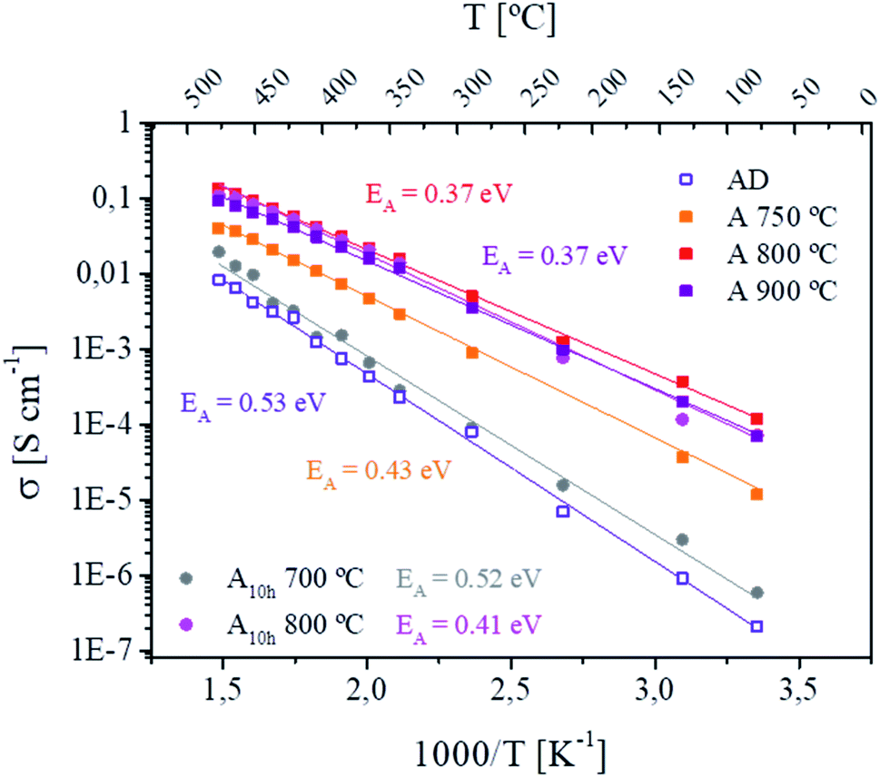 | ||
| Fig. 6 Arrhenius plot of different annealing conditions for LATP thin films deposited on Si3N4 substrates in PLD and their corresponding energies of activation (EA). If not differently indicated, dwelling has been applied for 5 h at the maximum temperature indicated. For samples annealed at 700 °C and 800 °C an extended dwelling of 10 h (see the subscript) has been performed in addition. | ||
For the future integration of our LATP films in realistic device architectures, we carried out measurements of the electrochemical stability window (Fig. S13†). The electrochemical stability window is in the range of 2.8–4.5 V, in good agreement with literature values,57,58 making them compatible with high voltage cathodes. Overall, and in light of our results, PLD becomes a competitive method to achieve high-quality LATP films comparable to the best reported films, realized through sputtering so far. Further understanding of the nature of the glassy intergranular matrix should be obtained to elucidate optimal compositions to achieve as high conductivities as reported for bulk samples.
Conclusions
We have demonstrated that large-area pulsed laser deposition is a well-suited technique to successfully deposit and engineer a dense thin film of LATP as a solid electrolyte for all-solid state battery applications with semi-industrial capabilities. Dense and stoichiometric thin films of 500 nm are achieved for depositions around 80 mTorr at 700 °C, showing a reduced presence of secondary phases. The ionic conductivities at room temperature for these as-deposited films are in the range of 10−7 to 10−6 S cm−1, which are about the same for state-of-the-art LiPON thin film electrolytes. After subjecting the layers to an annealing process at 800 °C, the ionic conductivity increased up to excellent values as high as 10−4 S cm−1 at room temperature. This is the highest value reported for partially crystallized LATP films to date and the first time that PLD is successfully employed to produce such films. We provide evidence that this enhancement might be caused by a lattice rearrangement during the annealing, resulting in an improved contact across interfacial domains of different orientations through the formation of amorphous phases at the grain boundaries. The preferred segregation of secondary phases to an intergranular matrix upon heat treatment can be driven by the inhibited acceptance of Li and Al inside the NASICON lattice, which presented Al-contents of 0.35 ≤ x ≤ 0.4 for the as-deposited thin films. As a result, the exact compositional character of the glassy phase appears to be variable for different stoichiometries of the local environment within the host material. Our work provides fabrication guidelines to achieve highly conducting LATP films through a careful engineering of the local environment of LATP crystallites, connected through an intergranular glassy ionic conducting matrix percolating through the film. In this context we suggest to concentrate on the stabilization of the amorphous intergranular phase at high temperatures and to limit the excessive segregation of aluminum outside the NASICON lattice. This is achieved especially by controlling annealing temperatures and dopant concentrations. Overall, the deposition of highly dense and homogeneous LATP layers with excellent ionic conductivity demonstrates the potential of NASICON-type thin film electrolytes for future all-solid-state batteries and microbatteries.Abbreviations
| LATP | Li1+xAlxTi2−x(PO4)3 |
| LTP | LiTi2(PO4)3 |
| AD | As-deposited |
| A | Annealed |
Conflicts of interest
The authors declare no competing financial interest.Acknowledgements
This project has received funding from the European Union's Horizon 2020 research and innovation program under grant agreement No. 824072 (HARVESTORE), from the European Regional Development Fund under the FEDER Catalonia Operative Programme 2014-2020 (FEM-IoT, 001-P-00166) and the “Generalitat de Catalunya” (2017 SGR 1421, NANOEN). FIB, HRSTEM, EDS and EELS studies were conducted at the Laboratorio de Microscopias Avanzadas, Universidad de Zaragoza, Spain. R. A. gratefully acknowledges the support from the Spanish Ministry of Economy and Competitiveness (MINECO) and the MICINN through project grants MAT2016-79776-P (AEI/FEDER, UE) and PID2019-104739GB-I00 as well as from the European Union H2020 program “ESTEEM3” (823717). J. C. G.-R., acknowledges the financial support provided by the European Union's Horizon 2020 research and innovation program under the Marie Skłodowska-Curie Grant Agreement No. 801342 (Tecniospring INDUSTRY), as well as by the Agency for Business Competitiveness of the Government of Catalonia. NMR measurements were supported and carried out at the Centre for Cooperative Research on Alternative Energies (CIC energiGUNE) as a member of the Basque Research and Technology Alliance (BRTA). Suitable Si3N4 substrates and microelectrodes have been provided by the Institute of Microelectronics of Barcelona IMB-CNM. Pt-covered Si substrates have been fabricated by the Interuniversity Microelectronics Centre (imec) in Leuven, Belgium. GI-XRD measurements have been collected at the Scientific and Technological Center (CCiT) at the University of Barcelona.References
- G. Liao, T. Mahrholz, S. Geier, P. Wierach and M. Wiedemann, J. Solid State Electrochem., 2018, 22, 1055–1061 CrossRef CAS.
- F. Soavi, L. G. Bettini, P. Piseri, P. Milani, C. Santoro, P. Atanassov and C. Arbizzani, J. Power Sources, 2016, 326, 717–725 CrossRef CAS PubMed.
- H. Ning, J. H. Pikul, R. Zhang, X. Li, S. Xu, J. Wang, J. A. Rogers, W. P. King and P. V. Braun, Proc. Natl. Acad. Sci. U. S. A., 2015, 112, 6573–6578 CrossRef CAS PubMed.
- F. Wu, P. Yu and L. Mao, Chem. Soc. Rev., 2017, 46, 2692–2704 RSC.
- X. Liang, F. Tan, F. Wei and J. Du, IOP Conf. Ser. Earth Environ. Sci., 2019, 218, 012138 CrossRef.
- M. Pasta, D. Armstrong, Z. L. Brown, J. Bu, M. R. Castell, P. Chen, A. Cocks, S. A. Corr, E. J. Cussen, E. Darnbrough, V. Deshpande, C. Doerrer, M. S. Dyer, H. El-Shinawi, N. Fleck, P. Grant, G. L. Gregory, C. Grovenor, L. J. Hardwick, J. T. S. Irvine, H. J. Lee, G. Li, E. Liberti, I. McClelland, C. Monroe, P. D. Nellist, P. R. Shearing, E. Shoko, W. Song, D. S. Jolly, C. I. Thomas, S. J. Turrell, M. Vestli, C. K. Williams, Y. Zhou and P. G. Bruce, JPhys Energy, 2020, 2, 032008 CrossRef CAS.
- C. Sun, J. Liu, Y. Gong, D. P. Wilkinson and J. Zhang, Nano Energy, 2017, 33, 363–386 CrossRef CAS.
- Y. Zhu, J. C. Gonzalez-Rosillo, M. Balaish, Z. D. Hood, K. J. Kim and J. L. M. Rupp, Nat. Rev. Mater., 2021, 6(4), 313–331 CrossRef CAS.
- M. Balaish, J. C. Gonzalez-Rosillo, K. J. Kim, Y. Zhu, Z. D. Hood and J. L. M. Rupp, Nat. Energy, 2021, 6, 227–239 CrossRef CAS.
- Z. Jiang, Q. Han, S. Wang and H. Wang, ChemElectroChem, 2019, 6, 2970–2983 CrossRef CAS.
- G. A. Nazri and G. Pistoia, Lithium Batteries: Science and Technology, Springer US, 2008 Search PubMed.
- D. Li, Z. Ma, J. Xu, Y. Li and K. Xie, Mater. Lett., 2014, 134, 237–239 CrossRef CAS.
- C. Wang, K. Fu, S. P. Kammampata, D. W. McOwen, A. J. Samson, L. Zhang, G. T. Hitz, A. M. Nolan, E. D. Wachsman, Y. Mo, V. Thangadurai and L. Hu, Chem. Rev., 2020, 120, 4257–4300 CrossRef CAS PubMed.
- R. Pfenninger, M. Struzik, I. I. Garbayo, E. Stilp and J. L. M. Rupp, Nat. Energy, 2019, 4, 475–483 CrossRef CAS.
- J. Sastre, A. Priebe, M. Döbeli, J. Michler, A. N. Tiwari and Y. E. Romanyuk, Adv. Mater. Interfaces, 2020, 2000425 CrossRef CAS.
- B. Lang, B. Ziebarth and C. Elsässer, Chem. Mater., 2015, 27, 5040–5048 CrossRef CAS.
- P. Hu, Z. Zou, X. Sun, D. Wang, J. Ma, Q. Kong, D. Xiao, L. Gu, X. Zhou, J. Zhao, S. Dong, B. He, M. Avdeev, S. Shi, G. Cui and L. Chen, Adv. Mater., 2020, 1907526 CrossRef CAS PubMed.
- Z. Liu, S. Venkatachalam, H. Kirchhain and L. van Wüllen, Solid State Ionics, 2016, 295, 32–40 CrossRef CAS.
- K. Arbi, M. Hoelzel, A. Kuhn, F. García-Alvarado and J. Sanz, Phys. Chem. Chem. Phys., 2014, 16, 18397–18405 RSC.
- G. X. Wang, D. H. Bradhurst, S. X. Dou and H. K. Liu, J. Power Sources, 2003, 124, 231–236 CrossRef CAS.
- M. Giarola, A. Sanson, F. Tietz, S. Pristat, E. Dashjav, D. Rettenwander, G. J. Redhammer and G. Mariotto, J. Phys. Chem. C, 2017, 121, 3697–3706 CrossRef CAS.
- H. Aono, J. Electrochem. Soc., 1990, 137, 1023 CrossRef CAS.
- D. Popovici, H. Nagai, S. Fujishima and J. Akedo, J. Am. Ceram. Soc., 2011, 94, 3847–3850 CrossRef CAS.
- L. Bai, W. Xue, Y. Y. Li, X. Liu, Y. Y. Li and J. Sun, Ceram. Int., 2018, 44, 7319–7328 CrossRef CAS.
- J. Maier, J. Power Sources, 2007, 174, 569–574 CrossRef CAS.
- P. Schaaf, Laser Processing of Materials: Fundamentals, Applications and Developments, Springer, Berlin and London, 2010, vol. 139 Search PubMed.
- J. A. Greer and M. D. Tabat, J. Vac. Sci. Technol., A, 1995, 13, 1175–1181 CrossRef CAS.
- H. Xia, H. L. Wang, W. Xiao, M. O. Lai and L. Lu, Int. J. Surf. Sci. Eng., 2009, 3, 23–43 CrossRef CAS.
- C. M. Julien and A. Mauger, Coatings, 2019, 9, 386 CrossRef CAS.
- R. Eason, Pulsed Laser Deposition of Thin Films: Applications-Led Growth of Functional Materials, John Wiley & Sons, 2007 Search PubMed.
- X. M. Wu, X. H. Li, S. W. Wang, Z. Wang, Y. H. Zhang, M. F. Xu and Z. Q. He, Thin Solid Films, 2003, 425, 103–107 CrossRef CAS.
- H. Chen, H. Tao, X. Zhao and Q. Wu, J. Non-Cryst. Solids, 2011, 357, 3267–3271 CrossRef CAS.
- G. Tan, F. Wu, L. Li, Y. Liu and R. Chen, J. Phys. Chem. C, 2012, 116, 3817–3826 CrossRef CAS.
- Y. Liang, C. Peng, Y. Kamiike, K. Kuroda and M. Okido, J. Alloys Compd., 2019, 775, 1147–1155 CrossRef CAS.
- P. Hofmann, F. Walther, M. Rohnke, J. Sann, W. G. Zeier and J. Janek, Solid State Ionics, 2019, 342, 115054 CrossRef CAS.
- H. Aono, E. Sugimoto, Y. Sadaoka, N. Imanaka and G. Adachi, J. Electrochem. Soc., 1990, 137, 1023–1027 CrossRef CAS.
- R. Arenal, F. de la Peña, O. Stéphan, M. Walls, M. Tencé, A. Loiseau and C. Colliex, Ultramicroscopy, 2008, 109, 32–38 CrossRef CAS PubMed.
- B. Key, D. J. Schroeder, B. J. Ingram and J. T. Vaughey, Chem. Mater., 2012, 24, 287–293 CrossRef CAS.
- S. Yu, A. Mertens, X. Gao, D. C. Gunduz, R. Schierholz, S. Benning, F. Hausen, J. Mertens, H. Kungl, H. Tempel and R.-A. Eichel, Funct. Mater. Lett., 2016, 9, 1650066 CrossRef CAS.
- A. Lakshmi-Narayana, O. M. Hussain, A. Mauger and C. Julien, Sci, 2019, 1, 56 CrossRef.
- K. Waetzig, A. Rost, U. Langklotz, B. Matthey and J. Schilm, J. Eur. Ceram. Soc., 2016, 36, 1995–2001 CrossRef CAS.
- M. Edén, Annu. Rep. NMR Spectrosc., 2015, 86, 237–331 CrossRef.
- S. K. Lee, S. B. Lee, S. Y. Park, Y. S. Yi and C. W. Ahn, Phys. Rev. Lett., 2009, 3–7 Search PubMed.
- S. Soman, Y. Iwai, J. Kawamura and A. Kulkarni, J. Solid State Electrochem., 2012, 16, 1761–1766 CrossRef CAS.
- K. Kwatek, W. Slubowska, J. Trebosc, O. Lafon and J. L. Nowinski, J. Eur. Ceram. Soc., 2020, 40, 85–93 CrossRef CAS.
- M. Forsyth, S. Wong, K. M. Nairn, A. S. Best, P. J. Newman and D. R. MacFarlane, Solid State Ionics, 1999, 124, 213–219 CrossRef CAS.
- A. D. Robertson, A. R. West and A. G. Ritchie, Solid State Ionics, 1997, 104, 1–11 CrossRef CAS.
- V. Lacivita, A. S. Westover, A. Kercher, N. D. Phillip, G. Yang, G. Veith, G. Ceder and N. J. Dudney, J. Am. Chem. Soc., 2018, 140, 11029–11038 CrossRef CAS PubMed.
- V. Lacivita, N. Artrith and G. Ceder, Chem. Mater., 2018, 30, 7077–7090 CrossRef CAS.
- J. Sastre, T. Y. Lin, A. N. Filippin, A. Priebe, E. Avancini, J. Michler, A. N. Tiwari, Y. E. Romanyuk and S. Buecheler, ACS Appl. Energy Mater., 2019, 2, 8511–8524 CrossRef CAS.
- E. Gilardi, G. Materzanini, L. Kahle, M. Döbeli, S. Lacey, X. Cheng, N. Marzari, D. Pergolesi, A. Hintennach and T. Lippert, ACS Appl. Energy Mater., 2020, 3, 9910–9917 CrossRef CAS.
- T. Famprikis, J. Galipaud, O. Clemens, B. Pecquenard and F. Le Cras, ACS Appl. Energy Mater., 2019, 2, 4782–4791 CrossRef CAS.
- H. Aono, E. Sugimoto, Y. Sadaoka, N. Imanaka and G. Ya Adachi, Solid State Ionics, 1993, 62, 309–316 CrossRef CAS.
- L. Le Van-jodin, F. Ducroquet, F. Sabary and I. Chevalier, Solid State Ionics, 2013, 253, 151–156 CrossRef CAS.
- M. G. S. R. Thomas, J. Electrochem. Soc., 1985, 132, 1521 CrossRef CAS.
- S. Breuer, D. Prutsch, Q. Ma, V. Epp, F. Preishuber-Pflügl, F. Tietz and M. Wilkening, J. Mater. Chem. A, 2015, 3, 21343–21350 RSC.
- F. Zheng, M. Kotobuki, S. Song, M. O. Lai and L. Lu, J. Power Sources, 2018, 389, 198–213 CrossRef CAS.
- W. D. Richards, L. J. Miara, Y. Wang, J. C. Kim and G. Ceder, Chem. Mater., 2016, 28, 266–273 CrossRef CAS.
Footnote |
| † Electronic supplementary information (ESI) available: XRD and Raman data on the target for PLD depositions; EDX analysis of LATP thin films deposited at different pO2; AFM images of the as-deposited and annealed thin films on Si3N4; XRD and Raman data for thin films of LATP deposited on Si3N4, SiO2 glass or Pt layers in comparison before and after annealing; XRD and GI-XRD of layers as-deposited and annealed at different temperatures; HAADF-HRSTEM images of AD and A samples and their corresponding FFTs; calculation of conductivities and the Arrhenius equation; in-plane impedance spectroscopy scheme for thin films; Arrhenius plot of different LATP electronic contributions identified on different substrates; degradation study for impedance spectroscopy on the LATP thin film; Arrhenius plot for pO2 dependent ionic conductivity study for LATP thin films as-deposited and annealed; XRD and Arrhenius plot of AD and A with various T-treatments to show reproducibility; Nyquist plots of EIS cross-plane measurements and the corresponding equivalent circuit; electrochemical stability window of LATP. See DOI: 10.1039/d1ta02991f |
| This journal is © The Royal Society of Chemistry 2021 |