All-inorganic perovskite quantum dots as light-harvesting, interfacial, and light-converting layers toward solar cells

Leimeng Xu a, Shichen Yuan b, Le Ma b, Baisong Zhang b, Tao Fang b, Xiansheng Li b and Jizhong Song *ab
aSchool of Physics and Microelectronics, Zhengzhou University, Zhengzhou 450052, China
bSchool of Materials Science and Engineering, MIIT Key Laboratory of Advanced Display Materials and Devices, Nanjing University of Science and Technology, Nanjing 210094, China. E-mail: songjizhong@njust.edu.cn

Received 4th April 2021 , Accepted 2nd June 2021

First published on 2nd June 2021


Abstract

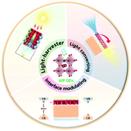
Solution-processed colloidal lead halide perovskite quantum dots (QDs) are considered one of the promising candidates for next-generation photovoltaics (PVs) due to the excellent optoelectronic properties and low-cost synthetic process. In particular, all-inorganic perovskite (AIP) QDs exhibit better prospects due to their better stability. Although remarkable breakthroughs have been made in bulk perovskite solar cells (SCs), the AIP QD-based SCs (AIPQDSCs) are still on their way to catch up. A lot of reports have summarized the development of perovskite SCs, but few have focused on AIPQDSCs. In this review, we focus on the latest development of AIPQDSCs, and analyze the current bottlenecks they are facing. Also, various optimization means have been discussed to improve the performance of AIPQDSCs from two perspectives of QD materials and device structure, including compositional regulation, surface engineering, interface engineering, and optimization of the carrier transport layer. In addition, AIP QDs as converter for SCs are also presented. Since the stability of perovskite SCs is currently the most pressing issue, the device stability is also highlighted. In the end, a brief summary and perspectives are presented to look forward to the future development of AIPQDSCs.


image file: d1ta02786g-p1.tif

Jizhong Song

Jizhong Song is a professor at the School of Physics and Microelectronics, Zhengzhou University. He received his Master's degree in material science and engineering from Shanghai University in 2011, and PhD in material science from Nanjing University of Aeronautics and Astronautics in 2015. His current research focuses on (i) the controlled synthesis of highly luminescent semiconductor nanocrystals; (ii) quantum dot surface chemistry; (iii) exploration of novel synthesis for nanomaterials; (iv) novel semiconductors for light-emitting diodes and photodetectors; (v) novel materials and concepts for optoelectronic devices. He has published around 80 peer-reviewed articles with over 10[thin space (1/6-em)]000 citations.


1. Introduction

As an emerging material, lead halide perovskite has attracted tremendous attention in recent years due to its excellent optoelectronic properties with long carrier diffusion lifetimes and low exciton binding energy, low-cost synthesis, as well as fine-tunable bandgap and emission spectra,1–3 which shows extraordinary potential in the fields of solar cells (SCs),4–7 light-emitting diodes,8–10 and photodetectors.11 Especially in SCs, great breakthroughs have been achieved in just a few years. To date, the highest efficiency of single-junction cells based on hybrid perovskites has reached 25.2% from best-research-cell-efficiencies of NREL, which is comparable to conventional silicon-based SCs, showing amazing prospects in photovoltaic (PV) applications. However, perovskite-based SCs (PSCs) are suffering from severe stability problems under harsh conditions (humidity, heat, oxygen, or illumination) or during long-time operation on account of the phase transitions or ion migration of perovskites.

Compared to bulk materials, low-dimensional QDs or nanocrystals (NCs) exhibit improved phase stability due to reduced surface strain.12–14 More importantly, colloidal QD-based PVs are promising for breaking the Shockley–Queisser theoretical efficiency limit of 33.7% via multiple exciton generation.15,16 Also, perovskite QDs have better defect-tolerance effect, which provide them a photoluminescence quantum yield (PLQY) near unity without additional passivation.17,18 In addition, the solution-processed colloidal perovskite QDs can be simply synthesized through a facile method without inert gas protection, showing better adjustability,19 and the as-crystallized colloidal QDs have better compatibility with various solution processing technologies for large-scale and flexible devices.20 The optoelectronic properties of perovskite QDs can be controlled by composition adjustment, dimensional size management, and surface-ligands regulation.21–23 These prominent characteristics make perovskite QDs more favorable for mass production and commercial applications.

AIP QDs, without any unstable organic components, exhibit better thermal stability (stable under ∼350 °C), which possess higher reliability for practical PV applications compared to their organic–inorganic counterparts.24 Since the first report of CsPbI3 NCs applied in SCs,14 rapid progress has been made in a short time;25 the highest power conversion efficiency (PCE) based on perovskite QDs has reached 16.6% to date.26 However, there is still a gap compared to that of their bulk materials. In addition, although AIP QDs show better stability, the stability issues also exist in QD-based SCs. In AIP QDs, α-CsPbI3 QDs with a band gap of 1.73 eV are the most suitable materials for absorption layers; however, they can easily transform into non-optically active δ-CsPbI3 (band gap is 2.82 eV) at room temperature or moisture air.25,27 Considerable efforts, including composition management, surface engineering, and interface optimization, have been devoted to stability research, but it has not yet been completely resolved, leaving substantial room for further improvement. A systematic summary of recent advances focusing on the improvement of the PV performance and stability will deepen our understanding toward feasible approaches to achieve highly efficient and stable PV devices. There are a lot of reviews on perovskite SCs but few papers are focused on AIP QDs.

In this review, we focus on AIP QDs and comprehensively summarize the latest progress of perovskite QDs in SCs not only as a light-absorbing layer but also as an interface optimizing and light-converting layer. Different promotion strategies for AIPQDSCs are presented, including compositional regulation, surface engineering, interface engineering, and transport layer optimization. Furthermore, the stability issues in AIPQDSCs are discussed. Finally, we analyze the current challenges faced by AIPQDSCs and look forward to their future development prospects. This review provides a comprehensive understanding of perovskite QDs in PV fields.

2. Features of all-inorganic perovskite QDs for SCs

Lead halide perovskites generally exist with the chemical formula of ABX3, where A represents monovalent cations such as Cs+ and Rb+, B represents divalent metal cation such as Pb2+, Sn2+, and Ge2+, and X represents monovalent halide anions I, Br, and Cl. Each site can be composed of a mixture of different ions. The crystalline structure of perovskite is shown in Fig. 1a, the excellent photoelectric properties of perovskite are mainly derived from the BX64− octahedron. For example, the conduction band minimum (CBM) and valence band maximum (VBM) in lead-based perovskites are mainly provided by the Pb-6p anti-bonding orbital and Pb-6s and X-p hybrid anti-bonding orbital, respectively (Fig. 1b).24 The electronic structure of perovskite is conducive for forming shallow defects, which make it highly defect tolerant.
image file: d1ta02786g-f1.tif
Fig. 1 The crystalline characteristics of AIP. (a) Schematic diagram of the AIP structure. (b) Contrast of the band edge contribution orbits between traditional semiconductors and perovskites. Adapted with permission from ref. 24 Copyright 2018, Nature Publishing Group. (c) Conversion conditions and relationships between α-, γ-, and δ-CsPbI3. Adapted with permission from ref. 28 Copyright 2019 Science Direct. (d) The anharmonic energy-displacement function, and band structures for α- and γ-CsPbI3. Adapted with permission from ref. 29 Copyright 2018, American Chemical Society.

As a photoelectric conversion device, SCs require semiconductor QDs in the active layer to possess a narrow band gap, high photoelectric conversion efficiency, facile synthetic methods, good stability toward light, heat, and electrolyte, and eco-friendly nature. The performance of SCs is closely related to the incident photon-to-electron conversion efficiency of the perovskite QD film. In general, the light-absorbing layer would excite electron–hole pairs after absorbing light, and then electrons and holes are extracted into the electron and hole transport layers. Therefore, the absorbing materials also need to have high light absorption coefficient, long charge-carrier diffusion length and lifetime, and low defect density. Perovskite QDs, which possess tunable bandgap, simple, and low-cost solution synthetic process, and excellent photoelectrical properties, are considered as an ideal PV material. However, the stability problem is still the key issue hindering the application of perovskites. In this section, we will discuss the stability problem of AIP QDs from the crystalline structure in detail. Meanwhile, the synthetic strategies and main photoelectric properties for SCs are also introduced.

2.1 Stability of all-inorganic perovskite QDs for SCs

Although AIP QDs show better stability compared to that with organic–inorganic hybrid components, the stability problems still exist, mainly in the following aspects. First, the phase structure is unstable due to the inadequate matching in I-based AIP QOs, which can easily transform into non-optically active phase at room temperature. Secondly, the easily lost surface ions and ligands due to the ionic crystal structure of perovskite can lead to the aggregation of QDs and enormous surface defects. Thirdly, thermodynamic instability due to the low formation energy of perovskites make them more susceptible to damage from the external environment, such as moisture, heat, or illumination. Analyzing the structural characteristics of perovskites can better help us to find a solution for the stability problem.

The application of SCs requires the absorbing layer to absorb the solar spectrum as much as possible, thus, the band gap of the absorption materials cannot be too wide. Compared to Br-based and Cl-based perovskites, I-based perovskites, such as α-CsPbI3 with a band gap of 1.73 eV, are more suitable for absorption layers. As an ionic crystal, the bond of perovskite does not have a definite orientation, which causes the perovskite to easily undergo phase change, especially when the structural distortion is severe. The radius of inorganic cations such as Cs is too small for an ideal perovskite structure compared with organic cations, which will cause serious structural distortion of α-CsPbI3, resulting in lower structural stability. The stable temperature of α-CsPbI3 is ∼620 K, and it is easy to phase transition to non-optically active δ-CsPbI3 (band gap is 2.82 eV) at room temperature or moisture air (Fig. 1c).13,28,30,31 Phase transition is a severe problem faced by AIP SCs. Perovskite QDs greatly release the internal strain, showing more advantages than bulk phase perovskite. Furthermore, the stability of black phase (α-, β-, or γ-) CsPbI3 QD can be greatly improved through composition adjustment and ligand engineering.

The composition adjustment of perovskites can be conducted following the Goldschmidt tolerance factor (t), which is expressed as

image file: d1ta02786g-t1.tif
where rA, rB, and rX are the ionic radii of A, B, and X, respectively.32 It is generally considered that the perovskite structure is stable when t is in the range of 0.813–1.107. If t is greater than 1, it means that the excessively large A-site ions will disassemble the 3D octahedral mesh into a series of layered octahedral networks to form 2D perovskites, such as PEA2PbI4. If t is too small, the A-site ions filled in the gap between the octahedrons cannot effectively support the octahedral mesh. For CsPbI3 (t = 0.81), the excessive distortion and vibration of the octahedral mesh can easily lead to the transformation from angle-sharing α-CsPbI3 (black phase) to edge-sharing δ-CsPbI3 (yellow phase). In addition, in the cooling process, α-CsPbI3 may turn into β and γ-CsPbI3 (black phase) with decreasing temperature instead of directly generating the stable phase δ-CsPbI3. Different from the double potential well instability of α-CsPbI3 in potential energy-displacement parameter function, γ-CsPbI3 is a metastable phase, as shown in Fig. 1d.29 It means that the lattice vibration of α-CsPbI3 can easily cause phase transitions, while γ-CsPbI3 has better stability and it is possible to prevent further phase transitions through appropriate strategies. Besides, DFT calculations show that the band gap of γ-CsPbI3 is slightly wider than α-CsPbI3 but it still maintains the characteristics of a direct band gap and then it will also exhibit strong light absorption performance comparable with α-CsPbI3 (Fig. 1d). Therefore, γ-CsPbI3 is also considered to have great development potential in the field of optoelectronics.

Furthermore, composition control is an effective way to improve the structural stability. For example, substituting Pb with a smaller radius atom, such as Sn or Ge, can also stabilize the crystal structure.33,34 However, the perovskite tends to lose its optical properties due to the easy oxidation of Sn or Ge divalent ions during the perovskite self-doping process. Therefore, the synthesis of Sn- or Ge-based perovskite QDs require additional oxidation suppression strategy, which adds to the complexity of the synthetic process. The composition substitution still needs further exploration.

Although perovskite QDs exhibit better stability than bulk perovskite materials for SCs,38 it is worth noting that the highly active surface states of perovskite QDs can easily lead to the formation of traps, which would capture carriers and result in serious energy loss. In a SC, the trap states will cause the photogenerated carriers to quickly recombine and release heat through the non-radiative recombination channel, reducing the efficiency and working life of the device. Therefore, the chemical activity of the surface states must be effectively suppressed. Surfactants are widely used in the synthesis of perovskite QDs to inhibit the overgrowth of QDs, passivate the defects of QDs, and prevent damage from external moisture and oxygen.36,39,40 Different ligands have different effects on improving the stability of QDs, which will be specifically discussed later.

In short, the obtained perovskite QDs must not only have a stable phase structure but also work efficiently and stably in the device.

2.2 Synthesis strategies

AIP QDs have flexible solution processability, thus, they have obvious cost advantages over traditional semiconductor QDs. The synthetic methods of AIP QDs generally include hot injection method,1 room-temperature anti-solvent method,41 and microwave synthesis method,42 among which the hot-injection method is the most widely used method.

The hot-injection method used for AIP QDs synthesis was firstly proposed by Protesescu1et al. in 2015. Taking CsPbI3 as an example, the synthetic diagram is shown in Fig. 2a. Under the protection of inert gas, cesium oleate is injected into the octadecene (ODE) solution of PbI2 with oleic acid (OA) and oleylamine (OAm) at 140–200 °C, where OA and OAm act as ligands to limit the overgrowth of QDs and passivate the surface defects, generally uncoordinated lead ions, which is considered to be a major deep trap that causes non-radiative recombination energy loss. The QDs synthesized by the hot-injection method have high PLQY and excellent size uniformity. In addition, the synthesis of AIP QDs with other halide components can be obtained only by the substitution of PbI2 with other halides or anion exchange35 (Fig. 2b). However, too many long-chain organic ligands will hinder the charge transport and seriously affect the electrical properties of QDs. Therefore, it is necessary to remove most of the organic molecules through a purification process, leaving only a few necessary ligands to prevent agglomeration and passivate the defects. Li et al. demonstrated that two hexane/ethyl acetate purifications could maximize the performance of the AIP QDs.43 Swarnkar et al. reported that the optoelectronic performance and stability of α-CsPbI3 were improved after methyl acetate purification, which remained phase stable under a low temperature of 77 K for more than 60 days at room temperature. The fabricated SCs exhibited open circuit voltage (Voc) of 1.23 V and a high efficiency of 10.77%.14


image file: d1ta02786g-f2.tif
Fig. 2 The synthesis strategies of AIP QDs. (a) Schematic diagram of the synthesis of QDs by hot injection method. (b) CsPbBr3 QDs are used as raw materials to synthesize CsPbX3 QDs by the anion-exchange method. Adapted with permission from ref. 35 Copyright 2015, American Chemical Society. (c) Schematic diagram of the synthesis of QDs at room temperature, and the ligands used. Adapted with permission from ref. 36 Copyright 2018 Wiley-VCH. (d) The ligand-mediated strategy for the synthesis of black phase CsPbI3 QDs at room temperature. Adapted with permission from ref. 37 Copyright 2021, Science Direct.

However, the hot-injection method is cumbersome and difficult to be used in large-scale production. Based on these problems, Li et al. proposed an anti-solvent synthesis method at room temperature.41 The precursor solution is first prepared by dissolving CsX and PbX2 in N,N-dimethylformamide (DMF) or dimethyl sulfoxide (DMSO), and OA and OAm are added into the solution as ligands. Then, the precursor is quickly injected into a large amount of toluene. Since the solubility of perovskite in toluene is far less than that in polar solvents, the perovskite crystals precipitate out quickly. The room-temperature synthesis method is conducive for large-scale production but the polar solvent in the dispersion will cause corrosion of the QDs, which causes high defect density and low quantum yield. In order to solve this problem, Song et al. proposed a room-temperature triple-ligand co-ordination method without polar solvents.36 Cesium octanoate was directly added into the precursor consisting of tetraoctylammonium bromide (TOAB) and PbBr2 dissolved in toluene, and dodecyl dimethyl ammonium bromide (DDAB) was injected into the reaction system to passivate the surface defects of the QDs (Fig. 2c), which generated QDs with PLQY of over 90%. However, this strategy cannot effectively synthesize black phase CsPbI3. Recently, they developed a ligand-mediated strategy based on this method using 4-dodecylbenzenesulfonic acid (DBSA) as the ligand to achieve the room temperature synthesis of γ-CsPbI3 NCs.37 In principle, the benzene ring and sulfonic acid group of DBSA have a large volume and strong bonding with perovskite surface atoms. Therefore, the steric hindrance effect of DBSA would inhibit the distortion of the octahedral framework and prevent the further phase transition of γ-CsPbI3 into δ-CsPbI3. The specific process is similar to the previous method; the difference is that DBSA is needed to be added to the cesium precursor, TOAB is replaced by the tetra-n-ethyl ammonium iodide (THAI) of the Pb precursor, and DDAB is replaced by OAmI to further passivate the QD surface, as shown in Fig. 2d. The development of room temperature synthesis is conducive for simplifying the process and reducing costs.

2.3 Photoelectric performance

SC is a photoelectric conversion device that converts sunlight energy to electrical energy. Its conversion efficiency is closely related to the performance of the absorption layer. The QDs used as absorption layer or converter in SCs require high absorption capacity, low trap density, and high photoelectric conversion efficiency. Meanwhile, QDs as an absorption layer require long charge-carrier diffusion length and lifetime, ensuring that the photo-generated carriers can be smoothly transport to the carrier transfer layer with less energy loss.

According to reports, the light absorption capacity of perovskite QDs is an order of magnitude higher than that of traditional organic dyes.44 Moreover, the band gap can be adjusted by the regulation of halide ion components by changing raw materials or anion exchange so as to obtain absorption and emission peaks in the range of 400–700 nm (as shown in Fig. 3a and b). Chiba et al. reported that red-emitting hybrid perovskite QD CsPb(Br/I)3 could be synthesized by adding organic iodide salt (oleylammonium iodide or aniline hydro iodide) into pre-synthesized CsPbBr3, which realized the conversion of the absorption peak from ∼510 nm to ∼650 nm. In addition, the optical properties of AIP QDs are greatly affected by their thermodynamic stability. The partial replacement of Pb with some divalent cations with less electronegativity can significantly improve the thermodynamic stability and reduce the trap density, thereby increasing the quantum yield. The DFT calculation results show that 2.8% Sr2+-doped CsPbBr3 with a formation energy of −6.93 eV has higher stability than undoped CsPbBr3 with a formation energy of −6.45 eV. Similarly, 20% Mn2+-doped CsPbI3 give a PLQY of ∼85%, which is much higher than that of undoped samples (∼62%).45


image file: d1ta02786g-f3.tif
Fig. 3 The photoelectric properties of AIP QDs. (a) Colloidal perovskite CsPbX3 NCs (X = Cl, Br, I) covering the entire visible spectral region with narrow and bright emission. (b) Representative PL spectra. Adapted with permission from ref. 1 Copyright 2015, American Chemical Society. (c) Schematic illustration of the changes in the ligand density, interparticle spacing, and surface defect density (depicted as red crosses) after purification and AET ligand exchange performed on CsPbI3 QDs. (d) IV curves for CsPbI3 and AET-CsPbI3 QD films. Adapted with permission from ref. 46 Copyright 2019, Wiley-VCH.

For semiconductors, the electrical transport performance is positively correlated with the carrier mobility. However, long-chain organic ligands on the surface of perovskite QDs as a highly insulating barrier can severely reduce the carrier diffusion and transport properties. It is necessary to replace long-chain ligands with good passivation and easily conductive short-chain ligands through ligand exchange (Fig. 3c). Bi et al. used the short-chain ligand 2-aminoethanethiol (AET) to perform ion exchange with the long-chain ligands OA and OAm, which significantly improved the conductivity of QDs, as shown in Fig. 3d.46

Although AIP QDs have a series of excellent photoelectric properties for PVs, the performance of the AIPQDSCs still need to be further improved. In the following discussion, we will introduce various strategies in detail for improving the efficiency of AIPQDSCs.

3. Compositional engineering for efficient SCs

Although solution-processed AIP QDs exhibit promising prospect for next-generation PVs due to their better stability, excellent tunability of optical properties, and near-unity PLQY, some remaining challenges need to be solved to obtain better PV performance. For instance, among various all-inorganic QDs, α-CsPbI3 exhibits an ideal optical bandgap (Eg) of 1.73 eV for PV applications. However, α-CsPbI3 is thermodynamically unstable at low temperature, which can be easily transformed into non-photoactive orthorhombic phase δ-CsPbI3 (Eg = 2.82 eV).50 For this problem, compositional engineering could be a valid strategy to stabilize the phase structure.51 In addition, composition control also provides an alternative to decrease the material defects and improve the energy conversion efficiency. Benefiting from the unique ionic crystal structure of perovskites, compositional management could be readily realized though cation or anion doping. In this section, doping at A, B, and X sites of all-inorganic perovskite QDs will be comprehensively discussed in QD-based SCs. Meanwhile, the latest developments in lead-free perovskite QD-based SCs will also be presented.

3.1 A-site regulation

Goldschmidt tolerance factor t[thin space (1/6-em)]51–53 is usually used to measure whether the crystal structure can exist stably theoretically. Generally, a t value between 0.9 and 1 is preferred to stabilize the cubic phase perovskites at room temperature. The selection of doping ions can be done based on this principle. In the typical perovskite ABX3 structure, single type of A-site ion may not be able to maintain a stable crystal structure at room temperature, such as α-CsPbI3, as we have mentioned above, A-site alloying could allow the tuning of the tolerance factor and maintaining the balance of the perovskite lattice. Moreover, alloying A-site cations can slightly adjust the crystal lattice, thus allowing for some control of the band gap, which would be necessary for the development of tandem SC architecture.

All-inorganic Cs-based perovskites exhibit better thermal stability preventing moisture, oxygen, or light radiation. However, the Cs+ cation is too small (t ≈ 0.81) to maintain a stable crystal lattice at room temperature. Doping larger A-site cation, such as FA+, and controlling the doping ratio could help to stabilize the lattice. Colloidal lead halide perovskite QDs possess a “soft” lattice and highly dynamic surface state, which provide a good platform for ion exchange; therefore, the mixed-cation Cs1−xFAxPbI3 perovskite QDs can be obtained through cation exchange. Hazarika and co-workers47 synthesized colloidal alloyed Cs1−xFAxPbI3 NCs via post-synthetic cation exchange, where colloidal CsPbI3 and FAPbI3 NC solutions were combined in appropriate proportions along with modest heating, and then, the cross exchange between the A-site cations resulted in desired compositions retaining their crystallographic framework, as shown in Fig. 4a. The SC device performance with different alloying proportions were also discussed; alloyed NC-based device shows high open-circuit voltage with a lower loss.


image file: d1ta02786g-f4.tif
Fig. 4 A-site regulation for AIPQDSCs. (a) Schematic diagram of the cross-exchange of Cs+ and FA+ ions between CsPbI3 and FAPbI3 perovskite NCs. Adapted with permission from ref. 47 Copyright 2018, American Chemical Society. (b) A-site cation-exchange reaction mechanism. Adapted with permission from ref. 38 Copyright 2020, Nature Publishing Group. (c) Performance of SC based on Cs1−xFAxPbI3 QDs of different compositions. (d) Distribution of PCE of SCs based on pure α-CsPbI3, pure FAPbI3, and stacked α-CsPbI3/FAPbI3 QD. Adapted with permission from ref. 48 Copyright 2019, American Chemical Society. (e) Vocversus bandgap of FA1−xCsxPb(I1−xBrx)3 PQDSC. Adapted with permission from ref. 49 Copyright 2019, American Chemical Society.

Similarly, the mixed-cation Cs1−xFAxPbI3 QDs were obtained through a ligand-assisted cation-exchange strategy, which could also control the doping ratio across the whole composition range (x = 0–1)38 (Fig. 4b). The incorporation of the FA cation made perovskite QDs more stable in ambient air or polar solvents; meanwhile, Cs1−xFAxPbI3 QDs exhibited longer carrier lifetime and lower non-radiative recombination. The resultant PV performance was greatly improved (Fig. 4c), where the Cs0.5FA0.5PbI3 QD SC achieved a record PCE of 16.6%, and they also exhibited greatly improved stability, which could retain 94% of the original PCE under continuous 1-sun illumination for 600 h.

In addition to using alloyed QDs to obtain more stable AIPQDSCs, Li et al.48 developed a combinational absorbing layer in AIPQDSCs using stacked α-CsPbI3 and FAPbI3 QDs, where A-site cation exchange at the interface would form a graded heterojunction for more efficient charge extraction. Two kinds of perovskite active layers would form a type-II band structure, where the graded VB is desirable for decreasing carrier recombination loss and improving carrier extraction. They achieved a high PCE of 15.6% (Fig. 4d). Combined A and X site alloying49 was explored to obtain a wide bandgap and high Voc for the application of a potential top cell in tandem junction SCs (Fig. 4e). Generally, controlling the A-site component in the perovskite lattice could help to stabilize the phase structure, regulating the bandgap and meanwhile providing an effective strategy to improve the performance of AIPQDSCs.

3.2 B-site regulation

Besides A-site doping, the B-site cation also plays a vital role in affecting the electronic properties and crystal structure of perovskite QDs because the B-site metal ion is involved in the important composition of the perovskite structure. Usually the typical B-site cation is Pb2+, which constitutes a [PbX6] octahedron with halogen X, and [PbX6] octahedrons form the basic framework of the perovskite structure. In addition, Pb contributes a lot to the electronic structure of the perovskite, in which the valence band maximum VBM is determined by the halide 3/4/5p and Pb 6s atomic orbitals and the CBM is mainly dominated by the Pb 6p atomic orbital.15,54,55 Therefore, changing the B-site cations can not only affect the crystal structure but also influence the optoelectronic properties.

Various metal ions have been introduced to replace Pb2+ in perovskite QDs or NCs to obtain the desired properties, such as Mn2+, Sn2+, and Sr2+.56–61 The selection of B-site doping ions must not only meet the required range of the tolerance factor t but also follow the evaluation criterion of octahedral factor, μ, which is expressed as

image file: d1ta02786g-t2.tif
where rB and rX correspond to the radii of B-site and X-site ions, respectively. Compared to A-site and X-site doping, B-site substitution is much more difficult owing to the high formation energy.62 According to the tolerance factor formula, smaller B-site doped cation would be preferred to replace Pb2+. Although B-site doping with various metal ions in α-CsPbI3 has been proved as a potential approach to stabilize the phase structure of colloidal CsPbI3 NCs or QDs, few have been applied in AIPQDSCs. Here, we introduce the current development of B-site doping in AIPQDSCs.

Zhang et al.50 successfully synthesized Zn-doped CsPbI3 QDs employing ZnI2 as the dopant (Fig. 5a). The incorporation of Zn in CsPbI3 QDs helped to increase the thermodynamic stability by the enhanced formation energy and Goldschmidt tolerance factor (Fig. 5b). Furthermore, the introduced additional I reduced the halogen vacancy of QDs, which made the QD film having reduced non-radiative recombination and improved PLQY. The Zn-doped CsPbI3-based AIPQDSCs achieved increased efficiency (from 13.98% to 16.07%) compared to pure CsPbI3 AIPQDSCs, accompanied with enhanced stability. Similarly, Bi et al.63 also reported the improved PCE and stability of SCs based on CsPb1−xZnxI3 QDs. They demonstrated that the doped Zn2+ ions improved the local ordering of the perovskite crystalline lattice, reducing the octahedral distortions, and Cl instead of I was used to passivate the vacancies of the perovskite QDs. In addition, GeI2 (ref. 34) was also used as the additive to synthesize CsPbI3 QDs with near-unity PLQY and improved chemical stability, and the obtained AIPQDSC exhibited an improved PCE of 12.15% and retained 85% of its peak performance over 90 days.


image file: d1ta02786g-f5.tif
Fig. 5 B-site regulation for AIPQDSCs. (a) Schematic illustration of Zn-doped CsPbI3 QDs and photographs of Zn:CsPbI3 QD solid-state films with different doping ratio under UV-light irradiation. (b) The calculated formation energies and Goldschmidt tolerance factors of CsPbI3 and Zn:CsPbI3 QDs. Adapted with permission from ref. 50 Copyright 2020, Wiley-VCH. (c) Atomic models of Sb:CsPbI3 cubes and platelets having 10 and 20% Sb (w.r.t. Pb) incorporation. Adapted with permission from ref. 62 Copyright 2019, American Chemical Society. (d) The crystal structure of Yb-doped CsPbI3 QDs. (e) EQE spectra of the SC based on CsPbI3, 20% Yb-doped, and 50% Yb-doped CsPbI3 QDs. Adapted with permission from ref. 64 Copyright 2019, The Royal Society of Chemistry. (f) The device performance of CsPbBr1.5I1.5 and Ag-doped CsPbBr1.5I1.5 QD-based SCs. Adapted with permission from ref. 65 Copyright 2021, American Chemical Society.

Some heterovalent B-site cations have also been used to improve the optoelectronic properties of perovskite QDs and stabilize the α-phase at the room temperature. Bera et al.62 introduced Sb3+ ions in the B-site of cubic CsPbI3 NCs in solution phase synthesis. Owing to the heterovalent substitution, only a limited amount of Sb3+ could actually enter the perovskite lattice. Even so, the insertion of Sb3+ could stabilize the crystal phase only with limited doping. With more intake, above ∼10% Sb3+ (w.r.t. Pb, ∼2.01% of total atoms) incorporation may disintegrate the shape from cubic to platelets (Fig. 5c) and quench the emission efficiency. An in situ Yb3+ doping strategy (Fig. 5d) was reported by Shi and co-workers64 to improve the material crystallinity and thermal stability, and reduce the number of defects and trap states caused by surface and lattice vacancies. Also, the Yb-doped AIPQDSC indeed achieved improved PCE and stability against the ambient environment, as shown in Fig. 5e.

Interestingly, monovalent Ag+ was also reported to substitute Pb2+ in CsPbBr1.5I1.5 QDs.65 Ghosh et al. presented that Ag+ had closer ionic radius (115 pm) to Pb2+ (119 pm) and partial substitution of Pb2+ by Ag+ did not perturb the crystal structure significantly. The substitution of Pb2+ with 3.5% Ag+ could reduce the intrinsic defect states and carrier recombination, thereby increasing the lifetime of the charge carriers. The alloyed AIPQDSC achieved ∼20% increase in the PCE (Fig. 5f) and sustained the PV performance for at least 575 h (24 days) with less than 5% drop in PCE.

Compared to A-site doping, the actual proportion of B-site doping cations into the perovskite lattice is very low but a small amount of B-site dopants will have a great impact on the structure and performance of the perovskite because of their important position. Although there have been several reports about the influence of B-site doping on colloidal perovskite QDs, their practical applications in SCs need further development.

3.3 X-site regulation

The optical properties of perovskite QDs can be widely tuned by adjusting the X-site halides (mainly Cl, Br, and I), which are involved in the electronic structure of the perovskite.24 Benefiting from the highly ionic crystal structure and dynamic surface properties of the perovskite QDs, the X-site component regulation can be realized by anion-exchange reactions without changing the shape, size, and crystal structure of the CsPbX3 QDs.35,66 There have been several summaries24,52,53,67 regarding the influence of X-site ions on the optical properties of perovskite colloidal NCs; we will not repeat them here. In this section, we focus on the application of X-site doping on the AIPQDSCs.

Cubic CsPbI3 exhibits the lowest bandgap (Eg = 1.73 eV) among the all-inorganic Pb-halide perovskite materials, which is optimal for PV.68 However, the cubic phase can easily transform into the orthorhombic phase (Eg = 2.82 eV), as mentioned above. Some researchers have demonstrated that the addition of Br (CsPbI3−xBrx) can reduce the phase transition temperature from over 300 °C to ∼110 °C69 and improve the phase stability. However, this incorporation of Br can also come at the expense of increasing the bandgap, which is not good for PV applications. Thus, it is the key to introduce an appropriate amount of the doping anion. Ghosh et al.70,71 discussed the influence of different proportions of Br in CsPbI3−xBrx on the performance of mixed-halide AIPQDSCs. Increasing Br made AIPQDSCs more stable but also reduced the efficiency. They demonstrated that CsPbBr1.5I1.5 was the best component to obtain AIPQDSCs with long-term stability and acceptable device performance with a slight compromise in the PCE.

To overcome the problem, Suri et al.49 proposed the combined A- and X-site alloying of wide bandgap FA1−xCsxPb(I1−xBrx)3 QDs that could increase the bandgap of mixed-halide perovskite QDs, improve charge transport in perovskite QD films, and reduce the voltage loss in AIPQDSC with Eg > 1.8 eV. Zhang et al.72 also used FAI post-treatment to improve the performance of mixed-halide perovskite CsPbI2Br1 QD-based SCs, which achieved long-term stabilized PCE beyond 14%. It could be seen that doping only X-site ions cannot meet the requirements of high-quality AIPQDSCs.

3.4 Lead-free perovskite

Indeed, lead halide perovskite QDs have promising application prospects due to their excellent properties in many aspects; however, the toxicity of lead has always been criticized. Thus, several studies have been carried out to explore their alternative elements. In general, lead-free perovskites include two categories, namely, Pb2+ replaced with equivalent cations such as Sn2+, Ge2+, Mn2+, and Cu2+,73–76 and with heterovalent cations, such as Sb3+, Bi3+, and Ag+.77–81 The currently prepared lead-free perovskite QDs have obtained satisfactory photoelectric properties; nevertheless, it is still under further exploration to obtain lead-free AIPQDSCs with high performance. Some attempts have been made to apply lead-free perovskite QDs in SCs.

Sn, which possesses the closest structural and electronic properties to Pb, is considered to be one of the most promising alternative candidates to replace Pb for future PV applications,82–84 which can meet the requirements of both low toxicity and high thermal stability due to its high decomposition temperature (∼450 °C). It should be noted that oxidation from Sn2+ to Sn4+ is a big issue for the further advancement of Sn-based perovskites. Wang et al.85 proposed a one-pot process to synthesize CsSnI3 QDs using triphenylphosphite (TPPi) as the antioxidant solvent additive to restrain the oxidation of Sn2+, as shown in Fig. 6a. The obtained CsSnI3 QD-based devices showed an average PCE of 4.13% with the highest PCE of 5.03% (Fig. 6b), which also exhibited negligible changes after long-time storage and testing. Chen and co-workers achieved a PCE of 12.96% using CsSnX3 quantum rods as the absorber layer.86


image file: d1ta02786g-f6.tif
Fig. 6 Lead-free perovskite PQDSCs. (a) Preparation of CsSnI3 QD solution. (b) Statistics of the PCE distribution of devices based on CsSnI3 bulk film and the CsSnI3 QD film. Adapted with permission from ref. 85 Copyright 2019, American Chemical Society. (c) Scheme of the Ge filling in the Sn vacancies and the replacement of Sn in CsSnI3 QDs. (d) Ultrafast transient absorption (TA) decays of CsSnI3 and CsSn0.6Ge0.4I3 NC films. Adapted with permission from ref. 87 Copyright 2020, Wiley-VCH. (e) The structural diagram of Cs2AgBiBr6 double perovskite. (f) The device structure of Cs2AgBiBr6 QDs as an absorber layer applied in AIPQDSC and (g) Corresponding device performance, inset is the photograph of the Cs2AgBiBr6 AIPQDSC. Adapted with permission from ref. 88 Copyright 2020, Springer Nature.

To solve the problem of instability and high-density surface vacancies of CsSnI3 QDs, co-alloyed CsSn0.6Ge0.4I3 was reported to improve the efficiency and stability of Sn-based AIPQDSC.87 The partial replacement of Sn atoms by Ge can passivate the Sn vacancies in Sn-based perovskite QDs and reduce the surface traps (Fig. 6c), leading to longer excitonic lifetime (Fig. 6d) and improved PLQY. The PCE of CsSn0.6Ge0.4I3-based AIPQDSC was improved to 4.9% compared to 3.1% for CsSnI3.

Besides the replacement of Pb with equivalent metal ions, the combination of monovalent metal (Na+, Ag+) and trivalent metal (Bi3+, Sb3+, In3+) was used to replace Pb, forming a special double perovskite structure. Although lead-free double perovskite NCs/QDs have been widely developed, only Cs2AgBiBr6 NCs (Fig. 6e) have been successfully incorporated in PV devices. Razi Ahmad et al.88 synthesized Cs2AgBiBr6 NCs with chemical and colloidal stability through a facile solution strategy, and the feasibility of Cs2AgBiBr6 NCs in PV applications was verified through a planar heterojunction SC with an n-i-p architecture, as shown in Fig. 6f. The device exhibited relatively low performance with a maximum PCE of 0.46% (Fig. 6g), which may be due to the inherent limitations of materials, such as less suitable optical and electronic properties. More efforts are needed for the development of lead-free perovskite QDs in PV applications.

4. Surface engineering for SCs

The synthesis of colloidal QDs usually employs a solution process, in which surface organic ligands play a vital role in controlling the crystal growth and colloidal stability. The perovskite QD surface is usually capped with long-chain ligands OA and OAm, which ensure that the QDs can be dispersed in the solvent uniformly and stably, and also passivate the surface defects of QDs. However, the long-chain and insulating ligands would trap the charges inside the QDs and hinder charge transfer between the QDs, leading to poor electronic coupling.71 From the perspective of electrical properties, the presence of surface ligands is detrimental to device performance. Thus, the surface regulation of QDs is of great importance to improve the properties of colloidal QDs and QD-based devices. In this section, we will discuss the impact of surface engineering on AIPQDSCs from the following two aspects: surface modification on colloidal QDs and on QD films.

4.1 Surface ligands for QDs

In terms of colloidal CsPbI3 QDs, long-chain organic ligands are essential for maintaining the stability and dispersion of NCs in solution during the synthetic process. However, as we have mentioned above, these organic surface ligands could impede charge transfer and result in poor electrical properties, especially for PV devices.89 Moreover, these surface ligands do not tightly bind with the surface atoms, which are highly dynamic and easily lost during the subsequent purification process;100 this may induce enormous surface defects and even lead to a phase transformation to δ-CsPbI3. Therefore, several efforts have been made to replace the long-chain OA and OAm with shorter ligands or novel molecules.90–93 There are two ways to modify the QD surface ligands: one is to use new ligands directly during synthesis process, and the other is to deal with the synthesized QDs through ligand exchange.94

For example, Chen et al.95 proposed a short-chain ligand-passivated α-CsPbI3 QDs for the improved efficiency of SCs. The adsorption energies of different ligands on the surface of QDs were compared (Fig. 7a), which exhibited that shorter octanoic acid/octylamine (C8) had stronger adsorption energy with the QD surface compared to that of OA/OAm (C18), resulting in enhanced PLQY and stability. The α-CsPbI3 QDs capped with C18/C8 (Fig. 7b) showed enhanced PLQY and stability due to the intensive combination between the surface ligands and the QDs. Moreover, the favorable surface passivation made the QD film an enhanced charge transport rate, which improved the PCE from 7.76% to 11.87% (Fig. 7c). Replacing long-chain OA/OAm with shorter ligands or ligands with stronger binding force during the synthetic process is an effective way to improve the device performance without sacrificing the QD stability.98 Some achievements have been made in colloidal QDs and QD for light-emitting diodes, though few have been applied in SCs.


image file: d1ta02786g-f7.tif
Fig. 7 Surface engineering for QDs in SCs. (a) Theoretical model for various ligands with different chain length adsorbed on the surface of α-CsPbI3 QDs. (b) Schematic of α-CsPbI3 QDs capped with C8/C18 ligands. (c) Electrical performance comparison of C18-CsPbI3 or C8/C18-CsPbI3 QD-based SCs. Adapted with permission from ref. 95 Copyright 2019, Wiley-VCH. (d) Schematic diagram of PTABr ligand passivation. (e) Time-resolved PL decays and (f) PCE of the PTABr-CsPbI3 controls sample, respectively. Adapted with permission from ref. 96 Copyright 2019, Wiley-VCH. (g) Schematic process of the perovskite QDs with and without SCN, and the corresponding (h) PV performance of the optimal SC. Adapted with permission from ref. 97 Copyright 2018, Cell Press.

Due to the highly dynamic surface state of perovskite QDs, it is easier to control the surface ligands through ligand exchange. Post-processing the synthesized QDs directly in solution can easily replace the long-chain ligands with shorter and binding-stronger ligands without destroying the crystal structure. Ionic ligands with halogen have been widely used in Br-based QDs,90,99 which are also applicative in I-based QDs for PV applications. For example, phenyltrimethylammonium bromide (PTABr)96 was introduced to partially (Fig. 7d) substitute the original long-chain ligands of the CsPbI3 QDs. The introduction of PTABr can not only shorten the length between the adjacent QDs but also passivate the halide vacancy defects of the QD by Br. The decreased defect densities provided the treated QDs with a longer exciton lifetime (Fig. 7e). The PCE of the passivated AIPQDSC was improved from 6.8% to 11.2% with PTABr-treatment (Fig. 7f). Bian et al.97 devised a hybrid passivation approach in which surface long-chain OA/Am of CsPbI3 QDs was exchanged with short-chain thiocyanate anion (SCN) in solution; the schematic of the exchange process is presented in Fig. 7g. The removal of long-chain OA/Am ligands and stronger chemical interaction between SCN and the QD surface could decrease the transport resistance and stabilize the phase structure. Combined with doping and other ligand treatments, the optimal device achieved a PCE of 14.45% (Fig. 7h).

Besides ligand exchange, some special additives have also been reported to crosslink the perovskite QDs for better charge transport channel and enhanced phase stability.103 In AIPQDSCs, μ-graphene (μGR)104 was applied in colloidal CsPbI3 QDs to crosslink QDs and form a μGR/CsPbI3 compositing film. Benefiting from the excellent electron mobility of μGR, electrons can easily pass between the cross-linked QDs along the μGR sheets, leading to accelerated charge extraction and reduced carrier recombination, and the PCE of the crosslinked AIPQDSC was greatly improved.

4.2 Post-treatment of solid films

Surface ligand engineering of colloidal perovskite QDs offers an effective way to optimize the PV performance of AIPQDSC; however, many problems will be induced during the process of depositing colloidal QDs into solid thin films. On one hand, amounts of defects would be introduced into the QD film due to the loss of surface ligands during the deposition process. On the other hand, the QD light-absorbing layer in AIPQDSC is required to be thick, which is usually fabricated through layer-by-layer deposition.14,105 The remaining ligands on the QD surface are still too much for charge transport; thus, the post-treatment of the QD film with specific solvents (such as methyl acetate, MeOAc) is generally needed to remove excess unreacted precursors and extra ligands without inducing agglomeration.14,26,106 Surface treatment and ligand exchange directly on the QD film seems to be a more effective strategy.

Sanehira et al.71 tuned the surface chemistry of CsPbI3 QD film via post-treatment with A-site cation halide (AX) salt, as shown in Fig. 8a. They showed that the AX salt could reduce the density of the original long-chain amine ligands and improve the coupling between QDs, which enhanced the carrier mobility in the QD film. Among the different AX salt post-treatments, treatments of FAI exhibited an optimal effect, which achieved a maximum PCE of 13.4% (Fig. 8b). Analogously, the layer-by-layer deposition method with FAI107 was reported to remove native ligands thoroughly, which enhanced the better coupling of neighboring QDs and improved the charge transport in solid-state films. Besides the AX salt, other cesium salts and alkali salts89,108 have also been used to post-treat the QD film and improve the performance of SCs.


image file: d1ta02786g-f8.tif
Fig. 8 Surface engineering for QD films in AIPQDSCs. (a) Schematic of the CsPbI3 QD film deposition process with AX salt post-treatment. (b) JV characteristics from forward bias to reverse bias of FAI-treated CsPbI3 QDSC. Adapted with permission from ref. 71 Copyright 2017, Science. (c) The schematic diagrams of enhanced electrical coupling between the GA-capped CsPbI3 QD solids as a result of reduced interdot distance. (d) Free carrier diffusion length of the CsPbI3 QD with and without GA treatments. (e) The effect of GA-matrix on PCEs of different QDSCs. Adapted with permission from ref. 101 Copyright 2020, Wiley-VCH. (f) Schematic illustrations showing the solid-state ligand exchange process of CsPbI3-QDs with different molecules. (g) JV curves of Ac-only exchanged, PEA-incorporated, and FA-incorporated CsPbI3 AIPQDSCs. Adapted with permission from ref. 102 Copyright 2020, Science Direct.

Ligand exchange with shorter chains or possessing special groups can not only effectively improve the carrier transport and recombination in the QD film but also stabilize the crystal structure. The guanidine (GA+)101 group combined with thermal annealing was applied in capping CsPbI3 QD solids, which helped to passivate the surface defects and facilitate the interparticle electrical interaction of QD solids. Better electrical coupling and charge transport was achieved due to closer packing (Fig. 8), leading to the remarkably enhanced charge mobility and carrier diffusion length (Fig. 8d), and consequently obtaining a champion PCE of 15.21% (Fig. 8e). In addition, some ligands with hydrophobic functional groups were introduced in perovskite QD films to simultaneously improve the efficiency and stability of SCs. Different hydrophobic ligands with cyclobenzene were reported102 to replace the original long-chain ligands of the CsPbI3 QD film (Fig. 8f), where the incorporation of short-chain and hydrophobic phenethylammonium (PEA) cations in the CsPbI3 QD film simultaneously led to improved PV performance and moisture stability compared to FA treatment (Fig. 8g). The PEA-incorporated CsPbI3-QD SCs showed a high PCE of 14.1% and high moisture stability, retaining over 90% of the initial performance after 15 days under ambient conditions.

In addition to ligand exchange, some functional polymer molecules were also introduced into QDs for better high-quality QD film and PV performance. Ji et al.109 added an optimal amount of conjugated polymers in the QD film to fabricate a polymer-QD bulk heterojunction hybrid layer at the interface of the QD layer and the hole transporting layer (HTL). The conjugated polymer molecules could effectively reduce pin-holes in the QD solid, leading to decreased carrier recombination loss and enhanced interfacial charge transfer. Furthermore, these conjugated polymers at the interface could adjust the energy level at the interface between QD and HTL for efficient hole transfer and electron blocking. As a result, the optimized AIPQDSC devices exhibited significantly enhanced short circuit current density and efficiency.

Not only the surface ligands but also the solvent used in the post-treatment also has a great influence on the QD film. The solvent used in the post-treatment is usually carboxylate esters; Cho et al.110 discussed the effects of carboxylate esters with different alkyl chain lengths on the ligand exchange in Br-based AIPQDSCs. They demonstrated that longer carboxylate esters resulted in more efficient ligand exchange with native long-chain ligands but at the same time, undesired less film thickness due to the stripping-out of the as-cast CsPbBr3 QDs was obtained. A mixed EtOAc/BuOAc solvent system was proposed to fabricate thick and pinhole-free CsPbBr3 QD solids for the improved performance of SCs.

In short, the post-treatment of the QD film provides more possibilities for device optimization. Unlike the complex environment of colloidal QDs located, it is easier to control the surface regulation of the QD solids without destroying the crystal structure by causing crystal aggregation. In addition, a single surface treatment method may not achieve optimal device effect, combining with multiple treatment strategies, such as simultaneous regulation of ligand exchange and solvent optimization, may bring the device performance to a higher level.

5. Device architectures

The typical perovskite QD SCs consist of five functional layers in conventional (n–i–p) configuration of FTO(ITO)/ETL/QDs/HTL/metal electrode or in the inverted (p–i–n) configuration of FTO(ITO)/HTL/QDs/ETL/metal electrode. The photo-generated current mainly includes the following processes: light absorption, exciton generation, exciton diffusion, exciton dissociation, carrier transport, and carrier collection. The perovskite QDs are used as absorbers to capture photons and generate excitons (electron–hole pairs); excitons migrate to the interface of the charge transport layer (CTL) and dissociate under the force of interfacial potential, forming the free carriers, while the carriers are transported and collected through the CTL, and finally pass through the electrodes to form a current. It shows that the acquisition of high-efficiency SC devices not only depends on the quality of the perovskite QDs but also the architecture of the devices. Therefore, besides optimizing the QD film, modulating and choosing proper CTL and optimizing the CTL/perovskite interface to accelerate charge extraction and transport and suppress carrier recombination are also significant for achieving high performance SCs.111 In this section, we will mainly discuss the effects of interface engineering regulation and the modulation of electron and hole transport layers on the performance of AIPQDSCs, and briefly illustrate the application significance of all-inorganic QDs as the interface layers in SCs.

5.1 Interfacial engineering

In general, PSCs conduct light-excited electrons and holes through the carrier transport layers (CTL) to the electrodes and generate the photocurrent. If free carriers are trapped or quenched by defects in the perovskite, ETL, or HTL, the device performance may deteriorate significantly. In this regard, controlling the CTL/perovskite interface can accelerate carrier transfer and inhibit recombination, which is conducive for improving the PV performance and environmental stability, and reducing the JV hysteresis characteristics.112–114 In addition, for AIPQDSCs, since QDs have large surface area and complicated environment, they can be in full contact with metal oxides and nano-carbides, and can also be used as absorbers for the photosensitization of QDs, which greatly improves the efficiency of energy utilization and charge transport efficiency.115 Therefore, adjusting the interface characteristics of inorganic perovskite QDs, passivating interface defects, accelerating separation, and extraction of carriers are of great significance for the realization of efficient and stable PSCs.89,95,116

At present, interface modification through a large number of functional materials has shown amazing effects in high-quality perovskite PSCs.117,118 For example, inserting CsBr into the interface of the CTL and the active layer can significantly restrain the defect-assistant recombination channel and improve the stability of the device.119 As one of the most successful and popular electron transport materials in PSCs, TiO2 exhibits many advantages but its instability under ultraviolet light easily corrodes inorganic perovskites and reduces the performance of PSCs.120,121 In addition, high sintering temperature and energy level matching are also challenges in the inorganic electron transport materials. Liu et al.122 inserted a layer of SmBr3 at the ETL/perovskite interface. As Sm interacted with oxygen in TiO2, a gradient energy-band structure was formed to block hole transport, which reduced carrier recombination and enhances charge transfer at the interface between ETL and the perovskite. The optimized interface promoted a pinhole-free and dense perovskite film, which inhibited charge recombination inside the perovskite. As a result, the PCE of the CsPbIBr2 PSCs was increased to 10.88%, which was 30% higher than that of unmodified PSCs. Furthermore, they also used μGR cross-linked QDs to form μGR/CsPbI3 thin films (Fig. 9a). The results showed that the synthesized QD film provided an effective channel for carrier transport and its electrical conductivity was greatly improved. Compared with the control device, the total PCE was increased from 10.41% to 11.40%, which shows an increase of 12% (Fig. 9b and c). The μGR cross-linking also greatly suppressed the instability caused by heat/humidity-induced QD agglomeration.104


image file: d1ta02786g-f9.tif
Fig. 9 Interfacial engineering of AIP QDs layers. (a) Schematic diagram of μGR's effects on charge transport and stability under moisture for the CsPbI3 film. (b) JV curves and related parameters of the devices with and without μGR. (c) EQEs and the integrated products of the EQE curve with AM1.5G photon flux. Adapted with permission from ref. 104 Copyright 2018, Wiley-VCH. (d) Device structure with the modification of the interface by LiF. (e) JV characteristics of inorganic CsPbI3−xBrx SCs with and without the LiF interlayer. Adapted with permission from ref. 124 Copyright 2019, Wiley-VCH.

In order to achieve high PCE, regardless of the PSCs architecture, interface engineering combined with CTL is often used to improve the energy level alignment, which promotes carrier transfer and extraction, and suppresses harmful interface carrier recombination on the metal or the organic/perovskite interface, and the aligned energy level structure can also effectively increase the Voc.97,123 You et al.124 used LiF as the barrier layer to significantly uplift the CBM of SnO2, while the surface defects of the perovskite were also inhibited (Fig. 9d). Great interface energy level arrangement and proper passivation made the Voc of inorganic PSCs as high as 1.25 V and the FF increase to 78.26% (Fig. 9e). The device maintained a stable output for more than 1000 h under the equivalent illumination of 1 sun (the efficiency drops less than 6%). Ma et al.109 introduced conjugated polymers into the colloidal AIP QDs to a polymer-QD bulk heterojunction mixed layer on the perovskite QD/hole transport layer (HTL) interface, which effectively reduced the pinhole density of the film, and the resulting device showed significantly enhanced short-circuit current density and efficiency. In addition, the highest occupied molecular orbital (HOMO) energy level of the conjugated polymer improved the interface carrier transport, thereby increasing the interface charge transfer efficiency and reducing the carrier recombination loss.

The charge selectivity of the interface layer can enhance the transport and extraction of the charges to the electrode and inhibit the reverse transfer of different types of carriers. Zhao et al.26 used the layer-by-layer deposition method to prepare heterogeneous A-site components in perovskite QDs. Heterostructure perovskite QD solid film greatly improved the charge separation and collection. They showed that light-induced electrons were easily driven into the perovskite QD solid film containing more FA+ cations, while the holes tended to be transferred to the higher Cs+ content perovskite QD solid film, thereby reducing the carrier recombination. In addition, modifying the perovskite absorber by introducing CsPbBr3 NCs was also an effective method to improve the perovskite heterojunction.125 CsPbBr3 NCs were the same as the perovskite absorber in terms of the crystal structure and stoichiometry. The improved carrier dynamics led to a significant increase in the PV performance of the corresponding devices.

5.2 Electron transport layer

The realization of SCs with high PCE depends on the rapid extraction and transfer of charge by the charge transport layer. Especially for the most common n-i-p type devices in PSCs, the selection and regulation of the ETL as the substrate for the upper perovskite layer plays an important role in the performance of the devices. Therefore, the ideal ETLs need to be equipped with high electron mobility, aligned band structure, low electron trap states, and good interface contact with the perovskite to inhibit interface recombination.126–128 So far, TiO2 is the most popular inorganic electron transport material owing to its matched energy band structure for perovskite and high transmittance in the visible region. Mesoscopic TiO2 (m-TiO2) and compact TiO2 (c-TiO2) are often used in combination as the ETL for perovskite SCs to achieve high PCE.129 The developed contact interface between m-TiO2 and the perovskite ensures an efficient electron extraction rate from the perovskite to the ETL. However, it is a challenge for perovskite QDs to fill into the interspaces of the m-TiO2 layers in a short time of the film formation process. Moreover, the large-roughness surface of m-TiO2 will lead to poor contact between the perovskite and m-TiO2, eventually resulting in serious interface recombination.

To resolve the above problems, Chen et al.130 adopted m-TiO2 modified by an electron-rich Cs+ containing methyl acetate solution as the ETL to construct the SC (Fig. 10a). Cs treatment significantly improved the interfacial properties of m-TiO2 and enabled the QDs to effectively migrate into m-TiO2. In addition, the introduction of Cs ions effectively passivates the defects in the QDs, which promotes charge migration from the QD to the ETL. The modified device exhibited three times higher electron injection rate than the unmodified m-TiO2 based SC. Eventually, the champion device with the best PCE value reaching 14.32% and Jsc of 17.77 mA cm−2 was achieved (Fig. 10b). Unfortunately, the high processing temperature, moderate electron mobility, and instability under ultraviolet light illumination of TiO2 restrict the further improvement of the device performance and the feasibility of fabrication for flexible devices.


image file: d1ta02786g-f10.tif
Fig. 10 Electron transport materials in AIPQDSCs. (a) Device structure of the mesoscopic CsPbI3 QD-based PSC. (b) Device performance of Cs-treated m-TiO2-based CsPbI3 QD SCs. Adapted with permission from ref. 130 Copyright 2020, American Chemical Society. (c) Energy band diagram of the corresponding CsPbI3-QD SCs based on Cl@SnO2. (d) Performance of device based on different HTLs. Inset is the corresponding device structure. Adapted with permission from ref. 25 Copyright 2021, American Chemical Society.

Nanostructured tin oxide (SnO2) is a suitable alternative for the ETL of AIP QD SCs, which is attributed to its high electron mobility, high transparency, good photostability, and suitable energy level. Jia et al.134 adopted the SnO2 layer prepared by the low-temperature solution method as the ETL of AIPQDSCs and the PCE of the device reached 13.66%. Compared with TiO2, SnO2 treated at low temperature showed potential as the ETL for flexible devices. However, SnO2-based devices exhibited lower PCE than other PCEs, which may be caused by surface electron trap states of SnO2. Lim et al. introduced Cl ion passivation of SnO2 QDs to reduce the surface defects and improved energy level of SnO2. The energy band diagram of the corresponding CsPbI3-QD SCs based on Cl@SnO2 is shown in Fig. 10c.25 Due to the reduction of interface defects and the decrease in the energy barrier, charge transfer from the light-absorbing layer to Cl@SnO2 was more rapid and efficient, as shown in the PL decay. Eventually, the Cl@SnO2-based AIPQDSC demonstrated enhanced performance with a PCE of 14.5% (Fig. 10d). Moreover, NiOx was also selected as an ETL to construct an inverted AIPQDSC. The device showed a high performance due to the minimal differences in the band energies between NiOx and CsPbI3 QDs.107

Compared with other perovskite SCs (such as organic–inorganic hybrid perovskite SCs and perovskite film based SCs), the performance of AIPQDSCs still has much room for improvement. Poor compatibility with the light-absorbing layer, high surface electron trap states, mismatched energy levels, and low charge mobility compared to the HTL still restrict the enhancement of the device efficiency.135 Therefore, it is significant to explore suitable electron transport materials for AIPQDSCs.

5.3 Hole transport layer

Similar to ETL, the HTL is responsible for extracting and transporting holes from the light-absorbing layer. Therefore, the selection of hole transport materials should meet the following conditions: (1) energy band structure of HTL matching with the perovskite; (2) high hole mobility to transfer the hole quickly; (3) blocking electrons to prevent interface recombination; (4) protecting the absorbent layer from degradation.136–138 Several p-type materials, such as organic small molecules, metallic compounds, and inorganic semiconductors, have been used as HTL for perovskite SCs. Among them, small organic molecule spiro-OMeTAD have been most widely adopted in perovskite SCs. However, spiro-OMeTAD still face the drawback of poor hole transport capability, which requires the use of dopants such as lithium salt (LiTFSI) and 4-tert-butylpyridine (tBP) to improve the performance.139 These additives are often hygroscopic and deliquescent, which seriously deteriorate the stability of the perovskite and the devices. In addition, the high price of spiro-OMeTAD due to the complex preparation process and high purity requirements cannot meet the requirements of commercial application. Although most of the high PCE for AIPQDSCs are based on spiro-OMeTAD as the HTL, there is still an urgent need to find suitable hole transport materials with good stability and simple treatment processes.140,141

Several dopant-free organic materials with excellent electrical properties have been developed for AIPQDSCs. Yuan et al. explored the performance of CsPbI3 QD SCs using poly-3-hexylthiophene (P3HT), poly[4,8-bis[(2-ethylhexyl)oxy]benzo[1,2-b:4,5-b′]dithiophene-2,6-diyl-alt-3-fluoro-2-[(2-ethylhexyl)carbonyl]thieno[3,4-b]thiophene-4,6-diyl] (PTB7), and poly[4,8-bis(5-(2-ethylhexyl)thiophen-2-yl)benzo[1,2-b; 4.5-b′]dithiophene-2,6-diyl-alt-3-fluoro-2-[(2-ethyl-hexyl)-carbonyl]-thieno[3,4-b]thiophene-4,6-diyl] (PTB7-Th) as the HTLs, and the energy level distribution of each material is shown in Fig. 11a. The hole transport materials have energy levels close to that of the perovskite layer, which result in effective hole extraction at the QDs/polymer interface. All the devices show repeatable and high PCE and low Voc loss. In particular, the device based on the BTB7 layer had a champion 12.55% PCE much higher than that of the spiro-OMeTAD-based device due to its more matched energy levels with the perovskite layer (Fig. 11b).142 Zeng et al.132 deposited P3HT on the top of the CsPbI2Br film to achieve electronic passivation of the defect state. As shown in Fig. 11c, the Stokes shift of CsPbI2Br/P3HT decreased from 35 nm to 29 nm compared with primal CsPbI2Br, indicating that the surface trap state of the perovskite film is effectively passivated. In addition, the energy disorder of annealed P3HT decreased and hole extraction was enhanced. Based on effective interface improvement and enhanced hole extraction performance, P3HT-based devices showed improved PV performance with a PCE of 12.02% (Fig. 11d). Compared with spiro-OMeTAD-based devices, P3HT devices exhibited enhanced Voc, representing a significant reduction in the energy loss.


image file: d1ta02786g-f11.tif
Fig. 11 Hole transport materials in AIPQDSCs. (a) Energy band diagram of CsPbI3-QD SCs with different polymeric hole conductors. (b) JV curves of devices based on PTB7; the illustration shows the corresponding device structure. Adapted with permission from ref. 142 Copyright 2018 Elsevier B.V. (c) The steady-state PL spectra for CsPbI2Br films with and without P3HT layer using a 405 nm laser as the excitation source. (d) The JV curves of the CsPbI2Br SCs based on P3HT and spiro-OMeTAD, respectively. Inset shows the histogram of Voc for the corresponding CsPbI2Br SCs. Adapted with permission from ref. 132 Copyright 2018, Wiley-VCH. (e) Device structure of Cu12Sb4S13 QDs-based CsPbI3 QD SC. (f) JV curves of the devices based on spiro-OMeTAD and Cu12Sb4S13 QDs, respectively. Adapted with permission from ref. 133 Copyright 2020, American Chemical Society.

Inorganic p-type semiconductors with outstanding characteristics, such as easy fabrication process, proper energy structures, high carrier mobility, good stability, and tuneable band gap, are promising candidates for HTL of AIPQDSCs. Cu12Sb4S13 QDs were selected as the HTL to replace spiro-OMeTAD for constructing the highly efficient CsPbI3 QD SCs (Fig. 11e).133 The crystal structure of Cu12Sb4S13 QDs is similar to that of CsPbI3 QDs with a very small lattice mismatch, which is conducive for pore extraction. Moreover, Cu12Sb4S13 QD after ligand exchange show stronger light capture ability and hole extraction ability, which further improved the Jsc of the device. Although there was a slight gap in the PCE between the final device and the spiro-OMeTAD-based device (Fig. 11f), the stability of the device was significantly improved, which provides a feasible idea for us to seek a suitable alternative to HTL.

5.4 All-inorganic QDs as interfacial layer for SCs

Interestingly, besides being a light harvester, QD materials have also been proved to be outstanding interface modifiers for constructing efficient and stable SCs.125 Based on their excellent performance, such as excellent charge carrier mobility, tunable energy-level structures, and designable surface chemistry for varying the functional ligands to control the interfacial charge transfer, QDs were used as interfacial modifiers between the CTL and the active layer to improve crystallization at the PSCs interface, passivate the surface defects and grain boundary trap, delay carrier recombination, optimize interface level, and promote charge separation/extraction.146

Wang et al. used CsPbI3 QDs as an intermediate between the ETL and the perovskite layer for introducing hybrid ligand interfacial layer on the perovskite films. After QD modification, the top surface of the perovskite films immediately generated band bending, which accelerated the charge transfer and reduced the energy loss, resulting in a Voc of 1.15 V and a power PCE of 20.6% for PSCs (Fig. 12a and b).143 Moreover, the modified device exhibited improved operation stability (Fig. 12c). Yang et al.147 combined zero-dimensional PQDs with three-dimensional perovskite films to passivate the surface defects in the perovskite films. In addition, QD made the surface morphology and potential of the perovskite more uniform, which was conducive for carrier dynamics between the perovskite film and the CTL. Finally, the device with more than 21% of the PCE was obtained.


image file: d1ta02786g-f12.tif
Fig. 12 AIP QDs as the interface layer. (a) Schematic diagram of the alloying reaction and the transfer of ligands to the perovskite surface by spin-coating CsPbI3 QDs onto the top surface of the perovskite film, (b) JV curves of the devices with the modification of CsPbI3 QDs. Adapted with permission from ref. 143 Copyright 2019 Wiley-VCH. (c) Schematic of the device architecture with modified QDs, (d) JV curves for the champion SC with modified QDs. Adapted with permission from ref. 144 Copyright 2019, Elsevier B.V. (e) Schematic representation of the growth procedure of perovskite films with the unmodified, CB-modified, and modified CsPbBr1.5I1.5, insets show the schematics of morphological evolution. (f) JV characteristics of the unmodified, CB-modified, and QD-modified devices. Adapted with permission from ref. 145 Copyright 2019, The Royal Society of Chemistry.

QDs can also be used to effectively engineer the interface between the perovskite and the HTL by passivating the defects, optimizing the energy-level alignment, and facilitating hole extraction of the PSCs. Akin et al.144 developed an effective and facile approach to modify the perovskite/HTM interface using interfacial CsPbBr1.85I1.15 QDs, and the device structure is shown in Fig. 12d. The QD interfacial material pulled holes from the inner perovskite layers to the interface by creating interfacial dipoles and enhanced hole transport ability, which resulted in an improved PCE of 21.14% with a solid increase in the FF and Voc (Fig. 12e). CsPbX3 QDs were also used as the interface layer between the HTL and the active layer. By controlling the position of the valence band between the perovskite layer and the interface layer, the cascade energy level structure was created and effective cavity injection from the active layer to the interface was realized. Compared with CsPbI3, CsPbBr3 had a more appropriate valence band position, thus significantly improving the PV characteristics of the device.131

In addition, QDs have also been used as an anti-solvent to control the crystallization process of the perovskite films. Ghosh et al. developed a method of antisolvent-cum-QD-assisted grain boundary modification to create monolithic grains. CsPbBr1.5I1.5 QDs were used to improve the crystallinity of the perovskite film by reducing the amorphous intergranular interface (Fig. 12f).145 In addition, the effective filling of QDs at the grain boundaries further reduced the interface defects and inhibited the formation of the recombination centers, which resulted in rapid charge transfer at the interface and achievement of SCs with improved PV features (Fig. 12g). In another study, CsPbBrCl2 QD dispersed in toluene was used to treat the MAPbI3 film in the crystallization process. The perovskite film obtained by this method showed favorable surface passivation and hydrophobic capacity, both of which were attributed to the surface covered with the OA ligand and a variety of elements in CsPbBrCl2 QDs. PSCs prepared with CsPbBrCl2 QDs exhibited a significantly increased PCE (from 18.30% to 20.90%) and enhanced stability.148

6. Converter for SCs

In addition to being used as an active layer for SCs, AIP QDs are also suitable as converters to optimize the performance of the SCs due to their high light absorption coefficient, high PLQY, and controllable photoluminescence.152–154 Long-term exposure to high-energy ultraviolet photons has been proved to damage the components of SCs, especially the organic components.155 In addition, in PSCs with mesoporous or planar sandwich structures, most UV photons are absorbed by transparent conductive substrates (e.g., FTO or ITO) and CTLs (e.g., TiO2 or ZnO), which have broadband gaps that allow UV light to be captured. This parasitic light absorption enhances the photostability of the PSCs but also reduces the light collection efficiency.156,157 By adding a conversion layer, the UV stability of the PSCs can be improved, and the parasitic absorption can be reduced and the efficiency can be improved.

Converters are often used in finished SCs in the form of an active photoluminescence layer. Their function is to absorb the solar photons that cannot be effectively captured and convert them into more suitable wavelengths without modifying the structure of the SCs or the inherent device materials.158 Therefore, AIP QD converters show great potential to be integrated with SCs to overcome the inherent low light absorption and heat loss.

At present, the converter based on AIP QDs has been widely studied. In this section, we will introduce the application of AIP QDs in SC converters, including the following three aspects: integration with traditional SCs, integration with perovskite SCs, and application in solar concentrators.60,159,160 The latest research progress in AIP QD converters is also presented.

6.1 Converters for conventional SCs

Traditional SCs, such as Si-based SCs, have been developed for many years and used in commercial applications. However, the utilization rate of SCs for solar energy is still not high; most photons whose energy is below the band gap energy cannot be absorbed, resulting in insufficient light energy utilization. Therefore, the inherent spectral loss leads to low efficiency of the PV cells, which is a huge challenge to further improve the performance of the devices.161 Combining with the AIP QD conversion layer will be a very promising strategy to improve the light energy utilization.

The converter can be obtained by simply spin coating AIP QDs on the surface of SCs. For example, Cao et al.162 synthesized CsPbBr3 QDs with the uniform size of 10 nm, and spin coated the colloidal QDs on the surface of commercial mc-Si SCs to obtain CsPbBr3 QDs/mc-Si hybrid SCs. Compared with mc-Si SCs, the external quantum efficiency of CsPbBr3 QDs/mc-Si SCs is significantly improved in the wavelength range of 300–500 nm and 700–1100 nm, and the maximum PCE of SCs is 14.52%.

However, when AIP QDs are used in the converter, they face the disadvantage of large reabsorption loss due to narrow band side emission, which reduces the emission efficiency. To overcome this problem, Mn2+ and Yb3+ ions were successfully doped into the perovskite lattice by replacing Pb2+, which effectively adjusted the photoelectric properties of the AIP QDs, and obtained larger Stokes' shift and higher quantum yield. For example, Wang et al.149 applied Mn2+-doped CsPbI3 QDs to the front end of polysilicon SCs to improve light collection in the short-wavelength region (Fig. 13a). They prepared 2.4% Mn2+-doped CsPbI3 QDs with Stokes' shift greater than 200 nm and high quantum yield (62%), which can effectively convert the low response spectrum in the ultraviolet region into ∼600 nm visible light and improve the photoelectric conversion efficiency of the device. The conversion efficiency of CsPbI3: Mn/polysilicon SCs was increased by 6.2% and the Jsc is increased by 5.1% because of the obvious improved quantum efficiency in the ultraviolet region (Fig. 13b). In addition, Abdelbar et al.163 also used Mn-doped CsPbI3 QDs as the interface frequency reduction layer of silicon nanopolymer SCs. As an efficient energy transfer center, CsPbCl3 NCs and Mn-doped CsPbCl3 NCs have blue light emission at 412 nm, which can realize the conversion of low-energy photons from the ultraviolet region below 400 nm to 412 nm, thus achieving a high PCE of 13.48%.


image file: d1ta02786g-f13.tif
Fig. 13 Converters for conventional SCs. (a) Schematic of a mc-Si SC module with an LDS layer on top. (b) ΔJsc, ΔPCE of the mc-Si SCs coated with various concentrations of CsPbCl3: Mn2+ QDs. Adapted with permission from ref. 149 Copyright 2018, Science Direct. (c) Schematic diagram of the perovskite film to enhance the PCE of the crystalline-silicon SCs. (d) PCE of SSCs coated with different perovskite QDs. Adapted with permission from ref. 150 Copyright 2017, Wiley-VCH. (e) Transmittance spectra of the QD film, IPCE curves of SSCs coated with different thicknesses of the perovskite films, and emission spectra of the QD film. Inset: Schematic diagram of the perovskite to enhance the PCE of SCs. (f) IV curves of SCs coated with different thicknesses of the QD film at a scan speed of 0.1 V s−1. Adapted with permission from ref. 151 Copyright 2020, Royal Society of Chemistry.

Sui et al.164 carried out further research and proposed the Mn-doped CsPbI3 NCs with different morphologies as converters for Cu(In, GA)Se2 SCs. QDs were synthesized from MnCl2 and PbCl2 in the ratio of 1[thin space (1/6-em)]:[thin space (1/6-em)]1, 1[thin space (1/6-em)]:[thin space (1/6-em)]2, 1[thin space (1/6-em)]:[thin space (1/6-em)]2.5, and 1[thin space (1/6-em)]:[thin space (1/6-em)]3. For samples with low Mn-doping content, the prepared samples are uniform nanocubes with an average particle size of 11 nm. When the MnCl2 content increased to more than 2.5, bulk nanosheets with ultra-thin thickness and strong quantum confinement effect were observed by TEM and AFM. At an optimum Mn doping level, the quantum yield of the CsPbI3 NCs was increased by 69%. The short-circuit current (6.67%) and PCE (1.67%) of Cu(In, GA)Se2 SCs were successfully increased using Mn-doped CsPbI3 NCs as the down-shifted layer.

In addition to Mn doping, Yb3+ and Ce3+ co-doped AIP QDs also show large absorption cross section, weak electron phonon coupling and high internal luminescence quantum yield (146%), which are suitable for solar energy converters. At the same time, Yb3+ and Ce3+ co-doped AIP QDs have strong absorption at 988 nm derived from Yb3+ ion, which can effectively improve the utilization of sunlight and enhance the efficiency of SCs. Zhou et al.150 successfully prepared Yb3+ and Er3+ co-doped CsPbCl1.5Br1.5 QDs, and self-assembled perovskite QDs onto the surface of commercial silicon SCs by simple liquid deposition method (Fig. 13c). The PCE of SCs increased from 18.1% to 21.5%, and the phase ratio increased by 18.8% (Fig. 13d). Integrating doped AIP QDs provides a cheap, convenient, and effective way to improve the PCE of silicon SCs method.

Ligand engineering has been greatly reported to improve the properties of converting AIP QDs so as to enhance the optical conversion ability and stability of doped QDs in SCs. For example, Sun et al.151 synthesized Mn-doped CsPbI3 QDs by introducing long-chain ammonium ligand dodecyl dimethyl ammonium chloride (DDAC). The DDAC ligand not only replaced the surface ligand of the QDs but also improved the efficiency and stability of Mn-doped QDs. The PLQY of CsPbCl3:Mn QDs reached as high as 91%, and the optical transmittance of ligand-modified CsPbCl3:Mn QD thin films (250 nm thickness) in the visible region is more than 95%. By self-assembling the modified QDs on the SC surface through liquid deposition, the PCE of silicon-based SCs (Fig. 13e) was effectively improved. By further adjusting the thickness of the QDs conversion layer, the PCE is increased from 19.64% to 20.65%, achieving an improvement of 5.14% (Fig. 13f). These successful strategies make great progress on conventional silicon SCs, which also indicates the huge potential in all-perovskite QD SCs.

6.2 Converters for perovskite SCs

In addition to the application in traditional SCs, AIP QD converters are also studied in perovskite SCs and further improve the performance of perovskite SCs.

By optimizing the performance of the AIP QD converter through doping and passivating strategies, the performance of SCs can be improved simply and directly. Mn-doped CsPbCl3 QDs has high quantum yield and large Stokes' shift, which is suitable for making the UV conversion layer.165 Wang et al.166 prepared CsPbCl3:Mn QDs with high quantum yield (∼60%) and large Stokes' shift (>200 nm) by hot-injection (Fig. 14a). CsPbCl3:Mn QDs could effectively convert the energy, which is usually wasted in the ultraviolet region (300–400 nm) into the visible light at ∼590 nm so as to improve the PCE and increase the short-circuit current (3.77%) and PCE (3.34%) (Fig. 14b). At the same time, the important loss mechanism of perovskite stability deterioration was eliminated by the conversion of ultraviolet light. The stability of perovskite SCs was improved from 85% to 97% after being irradiated by 5 mW cm−2 ultraviolet light for 100 h.


image file: d1ta02786g-f14.tif
Fig. 14 Converters for perovskite SCs. (a) On the left is the structural diagram of CsPbCl3:0.1Mn coated SCs, and on the right is the band gap alignment diagram of CsPbCl3:0.1Mn QDs. (b) IV curves for CsPbCl3:0.1Mn with different coated layer thickness-assisted perovskite SCs. Adapted with permission from ref. 166 Copyright 2017, American Chemical Society. (c) Schematic of the SC assembled with the CsPbCl3:(7.5 mol%) Cr3+, (12.1 mol%) Mn2+ converter film. (d) JV curves of bare SC, the PSC with the 270 nm CsPbCl3:(12.1 mol%) Mn2+ converter film, and the SC with the 270 nm CsPbCl3:(7.5 mol%) Cr3+, (12.1 mol%) Mn2+ film. (e) Normalized PCE as a function of time. Adapted with permission from ref. 167 Copyright 2020, Royal Society of Chemistry. (f) JV curves for the SCs coated with different layers of CsPbBr3 QDs. (g) UV light stability of the SCs with and without CsPbBr3 QDs coating. Adapted with permission from ref. 168 Copyright 2020, Science Direct.

Furthermore, Zhou et al.167 further used Cr3+ to passivate CsPbCl3:Mn perovskite QDs, which exhibited higher UV absorption. When the concentration of Cr3+ is 7.5 mol%, the best PLQY of CsPbCl3:Cr3+, Mn2+ perovskite QDs is 97%. The enhancement of PLQY can be attributed to the passivation of Cr3+ and the increase in the energy transfer rate from perovskite to Mn2+ (Fig. 14c). The PCE of treated SCs increased from 20.81% to 22.35% (Fig. 14d). The photoluminescence intensity of Cr3+, Mn2+ doped CsPbI3 QDs remained 98.5% after 10 days storage and 95% after 150 days storage, respectively, which was more stable than Mn2+ doped CsPbI3 QDs (Fig. 14e).

The direct application of pure AIP QDs without further treatment as UV-Vis conversion layer can also effectively improve the performance of the SCs. For example, Jin et al.168 coated CsPbBr3 QDs as UV-Vis conversion layer on the incident light side of organic–inorganic hybrid perovskite SCs; the PCE of the devices was increased by 3.46% and 20.02% compared with uncoated PSCs (Fig. 14f). At the same time, the CsPbBr3 QDs converter can reduce the damage of the perovskite layer caused by ultraviolet light. Uncoated and coated devices were exposed to 365 nm ultraviolet light (10 mW cm−2) for 200 h. Compared with uncoated PSCs, QDs-coated PSCs have excellent stability, which can maintain 90% initial efficiency, while uncoated devices only remain 48% initial efficiency (Fig. 14g).

6.3 Luminous solar concentrators

Besides being directly assembled with SCs by coating on the surface, AIP QDs are also suitable for light-emitting solar concentrators (LCSs) because they have displacement close to or higher than the unit PLQYs and large Stokes' shift, which can avoid self-absorption loss.171 Typical light-emitting solar concentrators are composed of transparent matrices (such as polymer or glass) embedded with high emission fluorescent groups (such as dyes, polymers, or QDs), which can be used for light-emitting and light conversion simultaneously. The solar radiation scattered in the space is concentrated, and the absorbed solar wavelength is converted so as to reduce the spectral loss and improve the efficiency of the SCs.172,173 LCSs are flexible, low-cost, lightweight, and translucent, which have great potential for building integrated PV devices.

LSCs can be obtained by simply inserting perovskite QDs into the polymer matrix. For example, Zhao et al.171 incorporated CsPb(BrxI1−x)3 QDs into dodecyl methacrylate ethylene glycol dimethacrylate polymer matrix to form a translucent composite, which exhibited an absorption spectrum in the range of 300–650 nm. By adjusting the chemical composition of Br/I, the Stokes' shift of QDs can be effectively increased, and the absorption and emission spectra can be better separated, with a high quantum yield of more than 60%. The prototype LSC based on perovskite CsPb(BrxI1−x)3 QDs showed an external optical efficiency of 2%. In addition, Zhao et al.174 combined carbon dots with mixed halide perovskite QDs for tandem LSCs. The series LSCs were prepared by the spectral tuning of c-dots and inorganic mixed halide perovskite QDs. Under sunlight (100 mW cm−2), the external optical efficiency of the series LSCs was about 3%, which was 27% higher than that of the single layer LSCs based on CsPb(BrxI1−x)3 QDs.

To meet the optical conversion requirements of LSCs, doping rare earth ions is a simple and effective strategy to optimize the AIP QDs. Luo et al.169 incorporated Yb3+ into CsPbI3 NCs, which had a PLQY of nearly 200% and exhibited almost zero PL photon self-absorption loss, and defined a new upper limit of 150% of the internal optical efficiency (ηint) of LSCs (Fig. 15a). A light-emitting concentrator of 25 cm2 was fabricated by CsPbI3:Yb NCs. The internal optical efficiency of the concentrator was 118.1 ± 6.7%, which was two times higher than that of the previous Mn-doped QDs. The sharp emission of the Yb3+ dopant at 990 nm matches the peak EQE of silicon SCs. The Yb-doped perovskite NCs were used to fabricate a large-area LSC with the size of more than 100 cm2, which achieved an external optical efficiency exceeding 10% (Fig. 15b). Yb3+-doped CsPb(Cl1−xBrx)3 NCs synthesized by Cohen et al.175 had a record PLQY of up to 200% and a large Stokes shift. CsPb(Cl1−xBrx)3 NCs-based double-layer LSCs exhibited 19% higher performance than that of single-layer CuInS2 LSCs with 70 × 70 × 0.1 cm3. Cai et al.170 doped Yb3+ into CsPbl3:Mn NCs; the resulting perovskite NCs showed a unique spectrum with three emission peaks, covering the UV/blue, visible, and near-infrared regions. By optimizing the doping concentration, the optimal PLQY of co-doped NCs can reach 125.3% (Fig. 15c). When only 2.2% incident photons are captured and guided to the edge region of Mn-doped CsPbI3 NCs LSC in sunlight, the light capture efficiency of Mn/Yb Co-doped CsPbI3 NCs LSC is nearly four times higher (Fig. 15d).


image file: d1ta02786g-f15.tif
Fig. 15 Luminous solar concentrators. (a) The top picture is the photo of LSC in sunlight and the photo of edge emission under ultraviolet radiation; the picture at the bottom shows the light conversion of Yb3+-doped NCs LSC. (b) Calculated flux gain (FG) for square-shaped QC-LSCs (thickness of 0.2 cm) with ηabs of 7.6% and ηPL of 200% (dark red solid line) as a function of the LSC size. Adapted with permission from ref. 169 Copyright 2019, American Chemical Society. (c) Schematic illustration of Mn2+/Yb3+ co-doped CsPbCl3 perovskite NCs. (d) The external optical efficiency (ηext) of the Mn-LSC and Mn/Yb-LSC devices under sunlight illumination. Adapted with permission from ref. 170 Copyright 2020, Wiley-VCH.

In addition, post-treatment can further improve the performance of AIP QD-based LSCs. Wu et al.176 proposed a novel triphenylphosphine (TPP) treatment strategy for perovskite LSCs; the PLQY of CsPbI3 NC polymer composite film increased significantly from 52% to 99.4 ± 0.4% after treatment, and the film remained stable even after long-term immersion in water (30 days) and strong mercury lamp irradiation (50 mW cm−2). Under the condition of geometric factor of 10, large-area (about 75 cm2) infrared LSCs were obtained, and the optical conversion efficiency was 3.1%.

7. Stability of SCs based on AIP QDs

Currently, the PV performance of SCs based on AIP QDs have achieved an increasing enhancement (Table 1). For example, SCs based on inorganic perovskite QDs were first introduced by the Luther group in 2016, who reported CsPbI3 QD devices with a respectable PCE of 10.77%.14 In 2019, a PCE of 16.07% (ref. 50) has been reported, which translates into a relative improvement of about 60% in efficiency achieved within just 4 years. Despite this impressive progress, the operational stability of these devices remains a key challenge, which requires significantly more research efforts.
Table 1 Summary of the PV performances of AIPQDSCs
AIP QD type Device structure PCE (%) V oc (V) J sc (mA cm−2) FF Ref.
CsPbI3 FTO/TiO2/QDs/spiro-OMeTAD/MoOx/Al 10.77 1.23 13.47 0.65 14
CsPbI3 FTO/TiO2/QDs/spiro-OMeTAD/MoOx/Al 13.43 1.16 15.24 0.76 71
CsPbI3 FTO/TiO2/QDs/PTAA/MoO3/Ag 15.21 1.251 15.85 0.77 101
CsPbI3 FTO/TiO2/QDs/PTB7/MoOx/Ag 12.55 1.27 12.39 0.80 131
CsPbI3 FTO/NiO/QDs/C60/ZnO/Ag 13.1 1.19 14.25 0.78 107
CsPbI3 FTO/TiO2/QDs/spiro-OMeTAD/Au 11.87 1.04 16.89 0.67 95
CsPbI3 FTO/Cl@SnO2/QDs/P3HT/MoOx/Ag 14.5 1.23 16.4 0.72 25
CsPbI3 FTO/TiO2/QDs/PTAA/MoO3/Ag 14.25 1.25 14.32 0.79 177
CsPbI3 FTO/TiO2/QDs/PTAA/MoOx/Ag 14.1 1.248 14.96 0.76 89
CsPbI3 ITO/SnO2/QDs/spiro-OMeTAD/Ag 13.66 1.22 17.66 0.63 134
CsPbI3 FTO/c-TiO2/s-m-TiO2/QDs/spiro-OMeTAD/Au 14.32 1.06 17.77 0.76 130
CsPbI3 FTO/c-TiO2/QDs/spiro-OMeTAD/Au 12.15 1.11 14.80 0.74 34
CsPbI3 FTO/TiO2/QDs/spiro-OMeTAD/MoOx/Al 13.47 1.18 15.50 0.73 47
CsPbI3 FTO/TiO2/mGR-QDs/PTAA/Au 11.64 1.18 13.59 0.72 104
CsPbI3 FTO/TiO2/QDs/PTAA/MoOx/Ag 14.9 1.24 15.84 0.75 178
CsPbI3 FTO/TiO2/QDs/PTAA/MoOx/Ag 13.8 1.22 15.10 0.75 109
Zn-doped CsPbI3 FTO/c-TiO2/QDs/spiro-OMeTAD/Mox/Al 16.07 1.23 17.58 0.74 50
Zn-doped CsPbI3 FTO/TiO2/QDs/spiro-OMeTAD/Ag 14.8 1.19 16.4 0.76 63
Yb-doped CsPbI3 FTO/c-TiO2/QDs/PTB7/MoO3/Ag 13.12 1.25 14.18 0.74 64
CsSnI3 FTO/PEDOT:PSS/QDs/PCBM/Ag 4.13 0.42 23.79 0.41 85
CsSn0.6Pb0.4I3 FTO/TiO2/QDs/spiro-OMeTAD/Au 2.9 0.63 10.13 0.46 179
CsPbBr3 FTO/ZnO/QDs/spiro-OMeTAD/Au 6.81 1.43 6.17 0.77 180
CsPbBr3 FTO/TiO2/QDs/spiro-MeOTAD/Au 5.4 1.5 5.6 0.62 181
CsPbBrI2 FTO/TiO2/QDs/PTAA/Au 12.39 1.19 12.93 0.80 123
CsPbBrI2 ITO/TiO2/QDs/P3HT/Au 12.2 1.20 14.22 0.71 106
CsPbI2+xBr1−x FTO/TiO2/QDs/PTAA/Au 14.45 1.20 14.45 0.79 97
CsPbI2Br ITO/TiO2/QDs/P3HT/Au 12.02 1.30 13.13 0.70 132


Similar to inorganic perovskite films, the degradation of SCs based on QDs can occur under numerous conditions,182–184 such as illumination, heat, moisture, oxygen, and bias. Beyond these external factors, both the intrinsic properties of QDs and their interplay with other materials present in PV devices can also serve as causes of degradation. While colloidal PQDs exhibit significantly enhanced phase stability at room temperature in comparison with their bulk counterparts,185 the stability of PV devices based thereon under operation has still emerged as the most urgent problem confronting the perovskite research community.

To tackle this issue, significant efforts have been invested by the scientific community.58,62,70,72,186 In this section, we will present the current efforts to enhance the stability and durability of SCs based on AIP QDs, mainly in view of three commonly-used fundamental strategies. The first one focuses on the PQD materials, which can be accomplished by compositional engineering or/and doping. The second strategy focuses on the surface treatment of QD films. The third strategy focuses on the optimization SC devices in order to protect the active absorber perovskite layer, for example, by optimizing the transporting layer and deposition procedures.

7.1 Compositional engineering for modulating the stability

Cs-based PQDs possess a low structural tolerance factor that is prone to undergo undesirable phase transitions. Therefore, adjusting the composition of perovskites to obtain appropriate tolerance factors can fundamentally improve the stability of the SCs. Usually, controlling the A-site, B-site, and X-site atoms relaxes the lattice strain, maximizes the formation energy of the vacancies, and suppresses the phase transitions.

In the aspect of A-site regulation, Cs-salt doping (e.g., with Cs acetate) of CsPbI3 QD films were shown to enhance the SC stability in air by filling the Cs vacancies at the QD surface.89 Aliovalent doping of silver ions65 at the lead site of CsPbBr1.5I1.5 QDs could improve the PV device stability. Ag doping is highly crucial for the reduction of surface and intrinsic defects, and decreasing non-radiative recombination. After 3.5% Ag doping, PV devices show extremely promising ambient stability for 575 h (24 days) with less than 5% drop in PCE in comparison to 12% drop for pristine QD devices (Fig. 16a and b).


image file: d1ta02786g-f16.tif
Fig. 16 Compositional engineering for stability. (a) Schematic representation of pristine and Ag-doped CsPbBr1.5I1.5 crystal structures. Vac indicates anion vacancy. (b) Stability plots for the devices monitored for 575 h (24 days) under an ambient environment. Adapted with permission from ref. 65 Copyright 2021, American Chemical Society. (c) PCE for different compositions of CsPbBr3−xIx QDs. Adapted with permission from ref. 70 Copyright 2020, Science Direct. (d) Electronic charge density for the pristine CsPbI3 and CsPb1−xZnxI3 slab with lead and iodide vacancy defects. (e) Ambient storage stability of the SCs without encapsulation. Adapted with permission from ref. 63 Copyright 2020, American Chemical Society.

B-site doping or alloying can increase the cohesive energy of perovskite QDs, which is highly conducive for increasing the stability. For example, Liu et al. used GeI2 as a dopant to avoid the formation of lead-rich surfaces in QDs and thus improve the QDs' stability due to the fact that the reduction of halide vacancies could decrease the surface defect density.34 Finally, GeI2-based AIPQDSCs presented excellent stability, which maintained 85% of the device efficiency after storage for 90 days. Alternatively, ytterbium doping has also been proposed as an effective defect passivation strategy for AIPQDSCs, leading to an enhanced stability of SCs operated in humid air.64 Tian et al.187 stabilized the cubic structure of perovskite CsPbI3 QD by doping metal cations Mn2+ and Zn2+ with smaller ion radius than that of Pb2+. The doping not only caused lattice constriction and increased the Goldschmidt tolerance factor of the perovskite structure but also enhanced the Pb–I binding energy, all of which improve the tolerance of phase transition. Moreover, the stability of the SC based on the doped QDs is significantly better than that of the control devices stored in ambient conditions.

In addition, when devices are under operation, light illumination and electric field changes induce ion migration towards the interfaces due to the low formation energy of the perovskite lattice, which lowered the device stability. Therefore, it is necessary to reduce the defects and increase the vacancy formation energy to suppress the migration, hence improving the device stability. Compared with the migration of A-site and B-site cations, the halide anions migrate more commonly due to their lower activation energy for ion migration. For example, CsPbI3 QDSCs maintained 98% of their starting PCE after one month of storage in a nitrogen-filled glovebox but when the same devices were exposed to 60% relative humidity, their PCE lost 90% of the initial value due to QD decomposition. Ghosh et al.70 found that the CsPb(I/Br)3 devices maintained 90% of their initial performance after 900 h of storage in a dry glovebox (Fig. 16c).

Furthermore, co-doping has been proven to be an effective strategy to enhance the SC stability. Tian et al.63 obtained colloidal AIP CsPb1−xZnxI3 QDs by the addition of ZnCl2. Synchrotron-based X-ray absorption fine structures demonstrated that the guest Zn2+ ions are doped into the QD structure to improve the local ordering of the lattice of the perovskite, reducing the octahedral distortions. Meanwhile, the Cl ions from ZnCl2 occupy the iodide vacancies of the perovskite to decrease the non-radiative recombination. The synergistic effect of doping makes QDs with ultralow density of the trap states. Consequently, SCs encapsulation retained a PCE of over 95% of the initial value after exposure to ambient conditions up to 50 h, while the PCE of the control device decreased to zero within 25 h (Fig. 16d and e). Similarly, an anion/cation synergy strategy50 was also proposed to improve the structural stability of the CsPbI3 QDs and reduce the pivotal iodine vacancy (VI) defect states. The synergistic effect of Zn2+ and I in CsPbI3 QDs can prevent the iodine loss during the fabrication of the QD film, inhibiting the formation of new VI defect states in the construction of the SCs. They found that the PCE of the control SC declined by about 38%, while for the doped QD SC, it was only 15%.

7.2 QD treatment for modulating the stability

Perovskite QDs are sensitive to polar solvents due to the ionic nature of the perovskite crystal structure. The surface atoms of perovskite QDs easily dissociate under the influence of polar solvents, causing surface defects and agglomeration of perovskite QDs.188 In addition, the surface ligand interaction with perovskite QDs was believed to be a highly dynamic and constantly changing system.189 Although QDs are capped by ligands, they are largely removed during the purification or device fabrication stages, resulting in surface vacancy defects.190 Moreover, the small size and large surface area of the QDs greatly amplifies the defects on the grain boundaries. Choosing proper capping ligands can inhibit perovskite QD aggregation under continuous illumination conditions, therefore avoiding the formation of non-radiative recombination centers, which capture charge carriers at the surface defects.191 Therefore, using functional molecules to passivate the surface defects of perovskite QDs is a promising strategy to improve the material stability.

For example, Kim et al. treated AIP QD solid films with PEAI to improve the hydrophobic stability of the films and meanwhile replace the original OAm ligands, which resulted in the PEAI-based AIP QD solid film having better stability than the FAI-based perovskite QD film.102 Thanks to the hydrophobic phenyl-terminated molecules, unencapsulated AIPQDSCs maintained 90% of the initial efficiency after 15 days. Yuan et al.192 developed an efficient post-treatment method using guanidinium thiocyanate (GASCN) to exchange the native capping ligands of the CsPbBr3 QDs. They further investigated the long-term stability of these CsPbBr3 QD-based SC without encapsulation under ambient conditions and the corresponding JV curves after storage for different days (Fig. 17a–c). After an initial small drop in the 1st week, the acetone and GASCN-treated devices showed excellent long-term stability and the efficiency remained almost 90% of the initial performance after 100 days of aging. Then, their group used the surface-passivated ligand anchoring strategy to treat the AIP QD films, and the corresponding devices could maintain good efficiency after ∼70 days of storage under ambient conditions (a low RH of <5%). The thiol group (–SH) can reduce the surface defect states and greatly improved the device stability (Fig. 17d and e).177


image file: d1ta02786g-f17.tif
Fig. 17 QD treatment for stability. (a) Schematic illustration of CsPbBr3 QD film deposition and solid-state post-treatment. (b) Long-term stability characterization of an optimal CsPbBr3 QD SC compared with the acetone-treated device. Inset images show the photographs of the corresponding optimal devices after storage for different days. (c) JV curves of the corresponding optimal device after storage for different days. Adapted with permission from ref. 192 Copyright 2020, American Chemical Society. (d) QD film stability of CsPbI3 QD based on MeOAc treatment (control) and 2-MP and 4-MP post-treatment. (e) Ambient stability of CsPbI3 QD SC devices based on MeOAc treatment (control) and 2-MP and 4-MP post-treatment under an RH of 20–30%. Adapted with permission from ref. 177 Copyright 2020, American Chemical Society.

Furthermore, amino acids134 were used as dual-passivation ligands to passivate the surface defects of CsPbI3 QDs using a facile single-step ligand exchange strategy. The perovskite QD solid films with amino acids as dual-passivation ligands could significantly improve defect passivation and therefore diminish charge carrier recombination in the perovskite QD solid. The evolution of the normalized PCE of the control and glycine-based AIPQDSCs was reported. After being stored for 10 days, about 55% of the original PCE was maintained in the control SC. In contrast, the glycine-based QDSC exhibits better stability than that of the control DSC, and about 87% of the original PCE was maintained. Similarly, Jia et al. passivated the surface defects of QDs with amino acid molecules, as a result of which the increased surface ligand density could protect the QDs from moisture.134

It is also a feasible approach to explore some suitable surface passivation molecules to provide a hydrophobic surface. Wang et al. crosslinked hydrophobic μGR with AIP QDs and the resulting AIPQDSCs showed much better stability under 60% humidity and 100 °C thermal stresses.104 In addition, the construction of core/shell structured AIP QDs also improved the stability of the QD films. Compared with a wide range of applications of core/shell structures in chalcogenide QDs, there is relatively little exploration of the core/shell structured AIP QDs. Thus, finding a suitable shell structure to improve the stability of the AIPQDSCs still remains a challenge.

7.3 Device engineering for modulating the stability

The rational design of devices could enhance the device stability. For example, the choice of the organic hole transport layer in the QDSCs can also strongly influence the overall stability of the device. Most of the devices employ spiro-OMeTAD as HTL, a well-known cause of degradation in perovskite PVs. One example of a promising substitute to spiro-OMeTAD is poly[[4,8-bis[(2-ethylhexyl)oxy]benzo[1,2-b:4,5-b′]dithiophene-2,6-diyl][3-fluoro-2-[(2-ethylhexyl)carbonyl]thieno[3,4-b]thiophenediyl]] (PTB7).142 Yang et al. demonstrated that polythiophene deposited on the top of CsPbI2Br QDs can significantly reduce electron–hole recombination within the perovskite, which is due to the electronic passivation of the surface defect states. They found132 that the unencapsulated polymer-modified devices exhibited great stability and retained around 90% of their initial PCE after 960 h of storage in a dry glovebox (Fig. 18a and b).
image file: d1ta02786g-f18.tif
Fig. 18 Device optimization for stability. (a) Device structure of CsPbI2Br SCs. (b) Long-term PCE stability of a CsPbI2Br SC without encapsulations stored in a dried glovebox and tested once a week in open air with a relative humidity of ≈15–40%. Adapted with permission from ref. 132 Copyright 2017, Wiley-VCH. (c) Normalized PCE obtained by stability tests of CsPbI3-QD SCs under light soaking (1-sun) conditions for unencapsulated devices of FTO/n-type/CsPbI3-QDs/P3HT/MoOx/Ag stored in 50% RH conditions. Adapted with permission from ref. 25 Copyright 2020, American Chemical Society.

Relatively, the inorganic hole transport layer could also enhance the device stability. For example, Chen et al. reported Cu12Sb4S13 QDs as hole transport materials133 to improve the device stability. They found that the photoelectric performance of spiro-MeOTAD-based AIPQDSCs declines rapidly and drops to 42% in 360 h, while Cu12Sb4S13 QD-based AIPQDSCs exhibit superior stability, maintaining 94% of their initial PCE under the same conditions.

In terms of ETL, chloride-passivated SnO2 QDs (Cl@SnO2 QDs) were used to replace the TiO2 nanoparticles, which are the most regularly used materials as ETLs in CsPbI3 QD PVs. Compared to the TiO2, Cl@SnO2 QDs have lower photocatalytic activity and few surface traps, which could obviously suppress the cubic-phase degradation of CsPbI3 QDs. The resultant CsPbI3 QD SCs based on Cl@SnO2 ETLs show significantly improved device operational stability (under conditions of 50% relative humidity and 1-sun illumination) compared to those based on TiO2 ETLs (Fig. 18c).25

In addition, the method by which SCs are fabricated can also directly affect their operational stability.193 The stability can be enhanced by the sequence of deposition of QD layers compared to layer-by-layer deposition because the washing steps that follow the deposition of each layer may introduce defects in the QD films and serve as additional pathways for degradation.194

8. Summary and perspectives

This review comprehensively summarized the recent development of AIPQDSCs from the perspective of materials and devices to improve the PV performance and device stability. Owing to the outstanding performance, phase stability, and low-cost synthesis, AIPQDs are competitive candidates for next-generation SCs; the efficiency of AIPQDSCs have achieved a great improvement from ∼10% to over 16% in a short time. However, there is still a certain gap between QD-based SCs and bulk device. Therefore, more efforts are needed to further improve the device performance. More urgently, the stability issue is a top priority in the field currently, which is being resolved for future commercial application. In addition, the toxicity of lead is also widely disputed; thus, looking for suitable substitutes is also a hotspot in the field. From our discussion, we have put forward following the suggestions for the future development of AIPQDSCs.

(1) Suitable surface and interface optimization for high efficiency. Since QDs have large specific surface area and dynamic surface states, the easily lost ligands can cause enormous surface defects, which lead to increased trapped carriers and non-recombination, thus resulting in low efficiency and photovoltage. Therefore, sufficient surface passivation is necessary but excessive organic ligands are adverse for charge transport. Thus, looking for surface ligands with stronger binding force and lower insulation is favorable for AIPQDSCs. Furthermore, ligand-exchange on QD films directly offers a more convenient strategy to improve the performance of the QD layer without damaging the crystal structure, which can also optimize the interface between the QD layer and the transport layer. Exploring suitable surface ligands and interface-treatment methods can effectively decrease the defect density and enhance carrier transport, thus leading to improved efficiency.

(2) Looking for the best component for AIPQDSCs. Appropriate component control helps to improve the stability of perovskite QDs. Some metal ions with lower electronegativity can be used to replace lead ions that can increase the formation energy of the system, improve the thermodynamic stability, and device lifetime. The smaller A-site inorganic ion results in lower structural stability, which can be solved by replacing or partially replacing Pb or X with smaller radius ions, or by adding a small amount of organic ions to replace Cs to achieve a balance between the decreasing thermal stability and the increasing phase stability.

(3) Optimizing the device structure. In addition to the material itself, the construction of the device is equally important. The matched energy levels between the functional layers and the high carrier mobility of the absorber and the transport layers in the device will improve the efficiency of carrier extraction and transport, while the transport layers need to effectively prevent the diffusion of another type of carrier. Secondly, good contact interface between the functional layers can effectively inhibit the capture of carriers by the defects and the non-radiative recombination at the interface. These lead to a diversified device design, which is highly desired.

(4) Exploring stable lead-free perovskite. Replacing Pb with non-toxic element in perovskites is a major research hotspot in the field. In the scheme of replacing lead, the lead-like element Sn or Ge with small radius is generally used. In addition, some new systems, such as double perovskite QDs, are also a feasible strategy. Compared with perovskites, double perovskites have higher stability but, at the same time, their low photoelectric performance restricts their development; even some double perovskites or other lead-free perovskite materials (such as Cs3Bi2I9) are indirect band gap semiconductors. Therefore, this needs to be adjusted through band engineering combined with experiments to improve their photoelectric performance.

(5) Developing flexible SCs. Flexible SCs have great potential in widespread applications such as portable electric chargers, wearable electronic devices, large-scale industrial roofing, and power sources for unmanned aerial vehicles. Colloidal QDs have low-cost synthesis and diversified solution processability, which is suitable for the construction of large-area and flexible SCs.

Finally, the commercialization of AIPQDSCs requires the realization of large-scale production processes. It is difficult to meet the production needs using the spin-coating methods commonly used in laboratories. Therefore, some new technologies, such as QD inkjet printing technology, squeegee coating, and pulling method covering, need new development and technical docking to realize industrial production and commercial applications.

Conflicts of interest

There are no conflicts to declare.

Acknowledgements

This work was financially supported by NSFC (51922049), the National Key Research and Development Program of China (2016YFB0401701), the Natural Science Foundation of Jiangsu Province (BK20180020), the Fundamental Research Funds for the Central Universities (30920032102).

Notes and references

  1. L. Protesescu, S. Yakunin, M. I. Bodnarchuk, F. Krieg, R. Caputo, C. H. Hendon, R. X. Yang, A. Walsh and M. V. Kovalenko, Nano Lett., 2015, 15, 3692–3696 Search PubMed.
  2. Y. Chen, H. Yi, X. Wu, R. Haroldson, Y. Gartstein, Y. Rodionov, K. Tikhonov, A. Zakhidov, X.-Y. Zhu and V. Podzorov, Nat. Commun., 2016, 7, 12253 Search PubMed.
  3. K. Galkowski, A. Mitioglu, A. Miyata, P. Plochocka, O. Portugall, G. E. Eperon, J. T.-W. Wang, T. Stergiopoulos, S. D. Stranks and H. J. Snaith, Energy Environ. Sci., 2016, 9, 962–970 Search PubMed.
  4. J. Yuan, X. Zhang, J. Sun, R. Patterson, H. Yao, D. Xue, Y. Wang, K. Ji, L. Hu, S. Huang, D. Chu, T. Wu, J. Hou and J. Yuan, Adv. Funct. Mater., 2021, 2101272 Search PubMed.
  5. J. Yuan, A. Hazarika, Q. Zhao, X. Ling, T. Moot, W. Ma and J. M. Luther, Joule, 2020, 4, 1160 Search PubMed.
  6. S. D. Stranks, G. E. Eperon, G. Grancini, C. Menelaou, M. J. Alcocer, T. Leijtens, L. M. Herz, A. Petrozza and H. J. Snaith, Science, 2013, 342, 341–344 Search PubMed.
  7. Y. Wang, M. I. Dar, L. K. Ono, T. Zhang, M. Kan, Y. Li, L. Zhang, X. Wang, Y. Yang and X. Gao, Science, 2019, 365, 591–595 Search PubMed.
  8. J. Song, T. Fang, J. Li, L. Xu, F. Zhang, B. Han, Q. Shan and H. Zeng, Adv. Mater., 2018, 30, 1805409 Search PubMed.
  9. J. Song, J. Li, X. Li, L. Xu, Y. Dong and H. Zeng, Adv. Mater., 2015, 27, 7162–7167 Search PubMed.
  10. T. Fang, T. Wang, X. Li, Y. Dong, S. Bai and J. Song, Sci. Bull., 2021, 66, 36–43 Search PubMed.
  11. L. T. Dou, Y. Yang, J. B. You, Z. R. Hong, W. H. Chang and G. Li, Nat. Commun., 2014, 5, 5404 Search PubMed.
  12. J.-W. Lee, Z. Dai, T.-H. Han, C. Choi, S.-Y. Chang, S.-J. Lee, N. De Marco, H. Zhao, P. Sun and Y. Huang, Nat. Commun., 2018, 9, 3021 Search PubMed.
  13. Q. Zhao, A. Hazarika, L. T. Schelhas, J. Liu, E. A. Gaulding, G. Li, M. Zhang, M. F. Toney, P. C. Sercel and J. M. Luther, ACS Energy Lett., 2019, 5, 238–247 Search PubMed.
  14. A. Swarnkar, A. R. Marshall, E. M. Sanehira, B. D. Chernomordik, D. T. Moore, J. A. Christians, T. Chakrabarti and J. M. Luther, Science, 2016, 354, 92–95 Search PubMed.
  15. J. Gan, J. He, R. L. Z. Hoye, A. Mavlonov, F. Raziq, J. L. MacManus-Driscoll, X. Wu, S. Li, X. Zu, Y. Zhan, X. Zhang and L. Qiao, ACS Energy Lett., 2019, 4, 1308–1320 Search PubMed.
  16. V. I. Klimov, Appl. Phys. Lett., 2006, 89, 123118 Search PubMed.
  17. A. Dutta, R. K. Behera, P. Pal, S. Baitalik and N. Pradhan, Angew. Chem., Int. Ed., 2019, 58, 5552–5556 Search PubMed.
  18. N. Mondal, A. De and A. Samanta, ACS Energy Lett., 2018, 4, 32–39 Search PubMed.
  19. F. Zhang, H. Zhong, C. Chen, X.-g. Wu, X. Hu, H. Huang, J. Han, B. Zou and Y. Dong, ACS Nano, 2015, 9, 4533–4542 Search PubMed.
  20. M. B. Wandel, C. A. Bell, J. Yu, M. C. Arno, N. Z. Dreger, Y.-H. Hsu, A. Pitto-Barry, J. C. Worch, A. P. Dove and M. L. Becker, Nat. Commun., 2021, 12, 446 Search PubMed.
  21. D. Yan, T. Shi, Z. Zang, T. Zhou, Z. Liu, Z. Zhang, J. Du, Y. Leng and X. Tang, Small, 2019, 15, 1901173 Search PubMed.
  22. J. Dai, J. Xi, L. Li, J. Zhao, Y. Shi, W. Zhang, C. Ran, B. Jiao, X. Hou and X. Duan, Angew. Chem., Int. Ed., 2018, 57, 5754–5758 Search PubMed.
  23. Y. Dong, Y.-K. Wang, F. Yuan, A. Johnston, Y. Liu, D. Ma, M.-J. Choi, B. Chen, M. Chekini and S.-W. Baek, Nat. Nanotechnol., 2020, 15, 668–674 Search PubMed.
  24. Q. A. Akkerman, G. Raino, M. V. Kovalenko and L. Manna, Nat. Mater., 2018, 17, 394–405 Search PubMed.
  25. S. Lim, J. Kim, J. Park, J. Min, S. Yun, T. Park, Y. Kim and J. Choi, ACS Appl. Mater. Interfaces, 2021, 13, 6119–6129 Search PubMed.
  26. Q. Zhao, A. Hazarika, X. Chen, S. P. Harvey, B. W. Larson, G. R. Teeter, J. Liu, T. Song, C. Xiao, L. Shaw, M. Zhang, G. Li, M. C. Beard and J. M. Luther, Nat. Commun., 2019, 10, 2842 Search PubMed.
  27. J. Tian, Q. Xue, Q. Yao, N. Li, C. J. Brabec and H. L. Yip, Adv. Energy Mater., 2020, 10, 2000183 Search PubMed.
  28. A. Ho-Baillie, M. Zhang, C. F. J. Lau, F.-J. Ma and S. Huang, Joule, 2019, 3, 938–955 Search PubMed.
  29. A. Marronnier, G. Roma, S. Boyer-Richard, L. Pedesseau, J.-M. Jancu, Y. Bonnassieux, C. Katan, C. C. Stoumpos, M. G. Kanatzidis and J. Even, ACS Nano, 2018, 12, 3477–3486 Search PubMed.
  30. G. E. Eperon, G. M. Paternò, R. J. Sutton, A. Zampetti, A. A. Haghighirad, F. Cacialli and H. J. Snaith, J. Mater. Chem. A, 2015, 3, 19688–19695 Search PubMed.
  31. Q. Ye, Y. Zhao, S. Mu, P. Gao, X. Zhang and J. You, Sci. China: Chem., 2019, 62, 810–821 Search PubMed.
  32. Y. Zhao and K. Zhu, Chem. Soc. Rev., 2016, 45, 655–689 Search PubMed.
  33. S. Liu, G. Shao, L. Ding, J. Liu, W. Xiang and X. Liang, Chem. Eng. J., 2019, 361, 937–944 Search PubMed.
  34. F. Liu, C. Ding, Y. Zhang, T. Kamisaka, Q. Zhao, J. M. Luther, T. Toyoda, S. Hayase, T. Minemoto, K. Yoshino, B. Zhang, S. Dai, J. Jiang, S. Tao and Q. Shen, Chem. Mater., 2019, 31, 798–807 Search PubMed.
  35. G. Nedelcu, L. Protesescu, S. Yakunin, M. I. Bodnarchuk, M. J. Grotevent and M. V. Kovalenko, Nano Lett., 2015, 15, 5635–5640 Search PubMed.
  36. J. Song, J. Li, L. Xu, J. Li, F. Zhang, B. Han, Q. Shan and H. Zeng, Adv. Mater., 2018, 30, 1800764 Search PubMed.
  37. T. Wang, X. Li, T. Fang, S. Wang and J. Song, Chem. Eng. J., 2021, 418, 129361 Search PubMed.
  38. M. Hao, Y. Bai, S. Zeiske, L. Ren, J. Liu, Y. Yuan, N. Zarrabi, N. Cheng, M. Ghasemi, P. Chen, M. Lyu, D. He, J.-H. Yun, Y. Du, Y. Wang, S. Ding, A. Armin, P. Meredith, G. Liu, H.-M. Cheng and L. Wang, Nat. Energy, 2020, 5, 79–88 Search PubMed.
  39. J. Song, L. Xu, J. Li, J. Xue, Y. Dong, X. Li and H. Zeng, Adv. Mater., 2016, 28, 4861–4869 Search PubMed.
  40. L. Pan, L. Zhang, Y. Qi, K. Conkle, F. Han, X. Zhu, D. Box, T. V. Shahbazyan and Q. Dai, ACS Appl. Nano Mater., 2020, 3, 9260–9267 Search PubMed.
  41. X. Li, Y. Wu, S. Zhang, B. Cai, Y. Gu, J. Song and H. Zeng, Adv. Funct. Mater., 2016, 26, 2435–2445 Search PubMed.
  42. Y. Li, H. Huang, Y. Xiong, S. V. Kershaw and A. L. Rogach, Angew. Chem., Int. Ed., 2018, 57, 5833–5837 Search PubMed.
  43. J. Li, L. Xu, T. Wang, J. Song, J. Chen, J. Xue, Y. Dong, B. Cai, Q. Shan and B. Han, Adv. Mater., 2017, 29, 1603885 Search PubMed.
  44. S. De Wolf, J. Holovsky, S.-J. Moon, P. Löper, B. Niesen, M. Ledinsky, F.-J. Haug, J.-H. Yum and C. Ballif, J. Phys. Chem. Lett., 2014, 5, 1035–1039 Search PubMed.
  45. S. Zou, Y. Liu, J. Li, C. Liu, R. Feng, F. Jiang, Y. Li, J. Song, H. Zeng and M. Hong, J. Am. Chem. Soc., 2017, 139, 11443–11450 Search PubMed.
  46. C. Bi, S. V. Kershaw, A. L. Rogach and J. Tian, Adv. Funct. Mater., 2019, 29, 1902446 Search PubMed.
  47. A. Hazarika, Q. Zhao, E. A. Gaulding, J. A. Christians, B. Dou, A. R. Marshall, T. Moot, J. J. Berry, J. C. Johnson and J. M. Luther, ACS Nano, 2018, 12, 10327–10337 Search PubMed.
  48. F. Li, S. Zhou, J. Yuan, C. Qin, Y. Yang, J. Shi, X. Ling, Y. Li and W. Ma, ACS Energy Lett., 2019, 4, 2571–2578 Search PubMed.
  49. M. Suri, A. Hazarika, B. W. Larson, Q. Zhao, M. Vallés-Pelarda, T. D. Siegler, M. K. Abney, A. J. Ferguson, B. A. Korgel and J. M. Luther, ACS Energy Lett., 2019, 4, 1954–1960 Search PubMed.
  50. L. Zhang, C. Kang, G. Zhang, Z. Pan, Z. Huang, S. Xu, H. Rao, H. Liu, S. Wu, X. Wu, X. Li, Z. Zhu, X. Zhong and A. K. Y. Jen, Adv. Funct. Mater., 2020, 31, 2005930 Search PubMed.
  51. A. O. El-Ballouli, O. M. Bakr and O. F. Mohammed, Chem. Mater., 2019, 31, 6387–6411 Search PubMed.
  52. J. Chen, D. Jia, E. M. J. Johansson, A. Hagfeldt and X. Zhang, Energy Environ. Sci., 2021, 14, 224–261 Search PubMed.
  53. F. Zhou, Z. Li, H. Chen, Q. Wang, L. Ding and Z. Jin, Nano Energy, 2020, 73, 104757 Search PubMed.
  54. Y. Chen and H. Zhou, J. Appl. Phys., 2020, 128, 060903 Search PubMed.
  55. L. Xu, S. Yuan, H. Zeng and J. Song, Mater. Today Nano, 2019, 6, 100036 Search PubMed.
  56. S. Das, A. De and A. Samanta, J. Phys. Chem. Lett., 2020, 11, 1178–1188 Search PubMed.
  57. Y. Chen, Y. Liu and M. Hong, Nanoscale, 2020, 12, 12228–12248 Search PubMed.
  58. J. Zhang, Y. Zhong, L. Chen and L. Yang, Chem. Phys. Lett., 2020, 752, 137572 Search PubMed.
  59. M. Lu, X. Zhang, Y. Zhang, J. Guo, X. Shen, W. W. Yu and A. L. Rogach, Adv. Mater., 2018, 30, 1804691 Search PubMed.
  60. Y. C. Kim, H. J. Jeong, S. T. Kim, Y. H. Song, B. Y. Kim, J. P. Kim, B. K. Kang, J. H. Yun and J. H. Jang, Nanoscale, 2020, 12, 558–562 Search PubMed.
  61. J. Li, J. Chen, L. Xu, S. Liu, S. Lan, X. Li and J. Song, Mater. Chem. Front., 2020, 4, 1444–1453 Search PubMed.
  62. S. Bera, D. Ghosh, A. Dutta, S. Bhattacharyya, S. Chakraborty and N. Pradhan, ACS Energy Lett., 2019, 4, 1364–1369 Search PubMed.
  63. C. Bi, X. Sun, X. Huang, S. Wang, J. Yuan, J. X. Wang, T. Pullerits and J. Tian, Chem. Mater., 2020, 32, 6105–6113 Search PubMed.
  64. J. Shi, F. Li, J. Yuan, X. Ling, S. Zhou, Y. Qian and W. Ma, J. Mater. Chem. A, 2019, 7, 20936–20944 Search PubMed.
  65. D. Ghosh, M. Y. Ali, A. Ghosh, A. Mandal and S. Bhattacharyya, J. Phys. Chem. C, 2021, 125, 5485–5493 Search PubMed.
  66. Q. A. Akkerman, V. D'Innocenzo, S. Accornero, A. Scarpellini, A. Petrozza, M. Prato and L. Manna, J. Am. Chem. Soc., 2015, 137, 10276–10281 Search PubMed.
  67. D. Yang, M. Cao, Q. Zhong, P. Li, X. Zhang and Q. Zhang, J. Mater. Chem. C, 2019, 7, 757 Search PubMed.
  68. G. E. Eperon, S. D. Stranks, C. Menelaou, M. B. Johnston, L. M. Herz and H. J. Snaith, Energy Environ. Sci., 2014, 7, 982–988 Search PubMed.
  69. S. Sharma, N. Weiden and A. Weiss, Z. Phys. Chem., 1992, 175, 63–80 Search PubMed.
  70. D. Ghosh, M. Y. Ali, D. K. Chaudhary and S. Bhattacharyya, Sol. Energy Mater. Sol. Cells, 2018, 185, 28–35 Search PubMed.
  71. E. M. Sanehira, A. R. Marshall, J. A. Christians, S. P. Harvey, P. N. Ciesielski, L. M. Wheeler, P. Schulz, L. Y. Lin, M. C. Beard and J. M. Luther, Sci. Adv., 2017, 3, eaao4204 Search PubMed.
  72. J. Zhang, Z. Jin, L. Liang, H. Wang, D. Bai, H. Bian, K. Wang, Q. Wang, N. Yuan, J. Ding and S. F. Liu, Adv. Sci., 2018, 5, 1801123 Search PubMed.
  73. Z. Luo, Q. Li, L. Zhang, X. Wu, L. Tan, C. Zou, Y. Liu and Z. Quan, Small, 2020, 16, 1905226 Search PubMed.
  74. H. Xu, J. Duan, Y. Zhao, Z. Jiao, B. He and Q. Tang, J. Power Sources, 2018, 399, 76–82 Search PubMed.
  75. I. Chung, J. H. Song, J. Im, J. Androulakis, C. D. Malliakas, H. Li, A. J. Freeman, J. T. Kenney and M. G. Kanatzidis, J. Am. Chem. Soc., 2012, 134, 8579–8787 Search PubMed.
  76. T. Cai, W. Shi, S. Hwang, K. Kobbekaduwa, Y. Nagaoka, H. Yang, K. Hills-Kimball, H. Zhu, J. Wang, Z. Wang, Y. Liu, D. Su, J. Gao and O. Chen, J. Am. Chem. Soc., 2020, 142, 11927–11936 Search PubMed.
  77. T. Geng, Z. Ma, Y. Chen, Y. Cao, P. Lv, N. Li and G. Xiao, Nanoscale, 2020, 12, 1425–1431 Search PubMed.
  78. S. E. Creutz, E. N. Crites, M. C. De Siena and D. R. Gamelin, Nano Lett., 2018, 18, 1118–1123 Search PubMed.
  79. W. Lee, S. Hong and S. Kim, J. Phys. Chem. C, 2019, 123, 2665–2672 Search PubMed.
  80. B. Pradhan, G. S. Kumar, S. Sain, A. Dalui, U. K. Ghorai, S. K. Pradhan and S. Acharya, Chem. Mater., 2018, 30, 2135–2142 Search PubMed.
  81. T. Fang, F. Zhang, S. Yuan, H. Zeng and J. Song, InfoMat, 2019, 1, 211–233 Search PubMed.
  82. X. H. Liu, K. Yan, D. W. Tan, X. Liang, H. M. Zhang and W. Huang, ACS Energy Lett., 2018, 3, 2701–2707 Search PubMed.
  83. T. B. Song, T. Yokoyama, S. Aramaki and M. G. Kanatzidis, ACS Energy Lett., 2017, 2, 897–903 Search PubMed.
  84. W. Ke, C. C. Stoumpos and M. G. Kanatzidis, Adv. Mater., 2019, 31, 1803230 Search PubMed.
  85. Y. Wang, J. Tu, T. Li, C. Tao, X. Deng and Z. Li, J. Mater. Chem. A, 2019, 7, 7683–7690 Search PubMed.
  86. L.-J. Chen, C.-R. Lee, Y.-J. Chuang, Z.-H. Wu and C. Chen, J. Phys. Chem. Lett., 2016, 7, 5028–5035 Search PubMed.
  87. M. Liu, H. Pasanen, H. Ali-Loytty, A. Hiltunen, K. Lahtonen, S. Qudsia, J. H. Smatt, M. Valden, N. V. Tkachenko and P. Vivo, Angew. Chem., Int. Ed., 2020, 59, 22117–22125 Search PubMed.
  88. R. Ahmad, G. V. Nutan, D. Singh, G. Gupta, U. Soni, S. Sapra and R. Srivastava, Nano Res., 2021, 14, 1126–1134 Search PubMed.
  89. X. F. Ling, S. J. Zhou, J. Y. Yuan, J. W. Shi, Y. L. Qian, B. W. Larson, Q. Zhao, C. C. Qin, F. C. Li, G. Z. Shi, C. Stewart, J. X. Hu, X. L. Zhang, J. M. Luther, S. Duhm and W. L. Ma, Adv. Energy Mater., 2019, 9, 1900721 Search PubMed.
  90. M. Imran, V. Caligiuri, M. Wang, L. Goldoni, M. Prato, R. Krahne, L. De Trizio and L. Manna, J. Am. Chem. Soc., 2018, 140, 2656–2664 Search PubMed.
  91. J. Pan, Y. Shang, J. Yin, M. De Bastiani, W. Peng, I. Dursun, L. Sinatra, A. M. El-Zohry, M. N. Hedhili, A.-H. Emwas, O. F. Mohammed, Z. Ning and O. M. Bakr, J. Am. Chem. Soc., 2017, 140, 562–565 Search PubMed.
  92. D. Yang, X. Li, W. Zhou, S. Zhang, C. Meng, Y. Wu, Y. Wang and H. Zeng, Adv. Mater., 2019, 31, 1900767 Search PubMed.
  93. J. Shi, F. Li, Y. Jin, C. Liu, B. Cohen-Kleinstein, S. Yuan, Y. Li, Z. K. Wang, J. Yuan and W. Ma, Angew. Chem., Int. Ed., 2020, 59, 22230 Search PubMed.
  94. T. Chiba, Y. Hayashi, H. Ebe, K. Hoshi, J. Sato, S. Sato, Y.-J. Pu, S. Ohisa and J. Kido, Nat. Photonics, 2018, 12, 681–687 Search PubMed.
  95. K. Chen, Q. Zhong, W. Chen, B. Sang, Y. Wang, T. Yang, Y. Liu, Y. Zhang and H. Zhang, Adv. Funct. Mater., 2019, 29, 1900991 Search PubMed.
  96. J. Yuan, C. Bi, S. Wang, R. Guo, T. Shen, L. Zhang and J. Tian, Adv. Funct. Mater., 2019, 29, 1906615 Search PubMed.
  97. H. Bian, D. Bai, Z. Jin, K. Wang, L. Liang, H. Wang, J. Zhang, Q. Wang and S. Liu, Joule, 2018, 2, 1500–1510 Search PubMed.
  98. F. Liu, Y. Zhang, C. Ding, S. Kobayashi, T. Izuishi, N. Nakazawa, T. Toyoda, T. Ohta, S. Hayase, T. Minemoto, K. Yoshino, S. Dai and Q. Shen, ACS Nano, 2017, 11, 10373–10383 Search PubMed.
  99. Y. Huang, W. Luan, M. Liu and L. Turyanska, J. Mater. Chem. C, 2020, 8, 2381–2387 Search PubMed.
  100. J. Xue, J.-W. Lee, Z. Dai, R. Wang, S. Nuryyeva, M. E. Liao, S.-Y. Chang, L. Meng, D. Meng, P. Sun, O. Lin, M. S. Goorsky and Y. Yang, Joule, 2018, 2, 1866–1878 Search PubMed.
  101. X. Ling, J. Yuan, X. Zhang, Y. Qian, S. M. Zakeeruddin, B. W. Larson, Q. Zhao, J. Shi, J. Yang, K. Ji, Y. Zhang, Y. Wang, C. Zhang, S. Duhm, J. M. Luther, M. Gratzel and W. Ma, Adv. Mater., 2020, 32, 2001906 Search PubMed.
  102. J. Kim, S. Cho, F. Dinic, J. Choi, C. Choi, S. M. Jeong, J. S. Lee, O. Voznyy, M. J. Ko and Y. Kim, Nano Energy, 2020, 75, 104985 Search PubMed.
  103. J. Byun, C. Satheeshkumar, G. Y. Lee, J. Oh, D. H. Jung, M. Seo and S. O. Kim, ACS Appl. Mater. Interfaces, 2020, 12, 31770–31775 Search PubMed.
  104. Q. Wang, Z. Jin, D. Chen, D. Bai, H. Bian, J. Sun, G. Zhu, G. Wang and S. F. Liu, Adv. Energy Mater., 2018, 8, 1800007 Search PubMed.
  105. L. M. Wheeler, E. M. Sanehira, A. R. Marshall, P. Schulz, M. Suri, N. C. Anderson, J. A. Christians, D. Nordlund, D. Sokaras, T. Kroll, S. P. Harvey, J. J. Berry, L. Y. Lin and J. M. Luther, J. Am. Chem. Soc., 2018, 140, 10504–10513 Search PubMed.
  106. C. Liu, Q. Zeng, Y. Zhao, Y. Yu, M. Yang, H. Gao, H. Wei and B. Yang, Sol. RRL, 2020, 4, 2000102 Search PubMed.
  107. S. B. Shivarudraiah, M. Ng, C. H. A. Li and J. E. Halpert, ACS Appl. Energy Mater., 2020, 3, 5620–5627 Search PubMed.
  108. J. Kim, B. Koo, W. H. Kim, J. Choi, C. Choi, S. J. Lim, J.-S. Lee, D.-H. Kim, M. J. Ko and Y. Kim, Nano Energy, 2019, 66, 104130 Search PubMed.
  109. K. Ji, J. Yuan, F. Li, Y. Shi, X. Ling, X. Zhang, Y. Zhang, H. Lu, J. Yuan and W. Ma, J. Mater. Chem. A, 2020, 8, 8104–8112 Search PubMed.
  110. S. Cho, J. Kim, S. M. Jeong, M. J. Ko, J.-S. Lee and Y. Kim, Chem. Mater., 2020, 32, 8808–8818 Search PubMed.
  111. L. Ma, B. Han, F. Zhang, L. Xu, T. Fang, S. Wang and J. Song, Appl. Mater. Today, 2021, 22, 100946 Search PubMed.
  112. M. K. Otoufi, M. Ranjbar, A. Kermanpur, N. Taghavinia, M. Minbashi, M. Forouzandeh and F. Ebadi, Sol. Energy, 2020, 208, 697–707 Search PubMed.
  113. T. Wang, T. Fang, X. Li, L. Xu and J. Song, J. Phys. Chem. C, 2021, 125, 5475–5484 Search PubMed.
  114. Y. Wang, C. Duan, X. Zhang, N. Rujisamphan, Y. Liu, Y. Li, J. Yuan and W. Ma, ACS Appl. Mater. Interfaces, 2020, 12, 31659–31666 Search PubMed.
  115. J.-H. Im, C.-R. Lee, J.-W. Lee, S.-W. Park and N.-G. Park, Nanoscale, 2011, 3, 4088–4093 Search PubMed.
  116. L. Xu, J. Li, B. Cai, J. Song, F. Zhang, T. Fang and H. Zeng, Nat. Commun., 2020, 11, 3902 Search PubMed.
  117. Z. Zhu, J. Ma, Z. Wang, C. Mu, Z. Fan, L. Du, Y. Bai, L. Fan, H. Yan and D. L. Phillips, J. Am. Chem. Soc., 2014, 136, 3760–3763 Search PubMed.
  118. J. Duan, Y. Zhao, B. He and Q. Tang, Angew. Chem., Int. Ed., 2018, 130, 3849–3853 Search PubMed.
  119. W. Zhu, Z. Zhang, W. Chai, Q. Zhang, D. Chen, Z. Lin, J. Chang, J. Zhang, C. Zhang and Y. Hao, ChemSusChem, 2019, 12, 2318–2325 Search PubMed.
  120. H. Tan, A. Jain, O. Voznyy, X. Lan, F. P. G. d. Arquer, J. Z. Fan, R. Quintero-Bermudez, M. Yuan, B. Zhang, Y. Zhao, F. Fan, P. Li, L. N. Quan, Y. Zhao, Z.-H. Lu, Z. Yang, S. Hoogland and E. H. Sargent, Science, 2017, 355, 722–726 Search PubMed.
  121. Y. Zhao, H. Zhang, X. Ren, H. L. Zhu, Z. Huang, F. Ye, D. Ouyang, K. W. Cheah, A. K. Y. Jen and W. C. H. Choy, ACS Energy Lett., 2018, 3, 2891–2898 Search PubMed.
  122. W. S. Subhani, K. Wang, M. Du, X. Wang and S. Liu, Adv. Energy Mater., 2019, 9, 1803785 Search PubMed.
  123. J. Zhang, D. Bai, Z. Jin, H. Bian, K. Wang, J. Sun, Q. Wang and S. Liu, Adv. Energy Mater., 2018, 8, 1703246 Search PubMed.
  124. Q. Ye, Y. Zhao, S. Mu, F. Ma, F. Gao, Z. Chu, Z. Yin, P. Gao, X. Zhang and J. You, Adv. Mater., 2019, 31, 1905143 Search PubMed.
  125. H. Zai, C. Zhu, H. Xie, Y. Zhao, C. Shi, Z. Chen, X. Ke, M. Sui, C. Chen, J. Hu, Q. Zhang, Y. Gao, H. Zhou, Y. Li and Q. Chen, ACS Energy Lett., 2017, 3, 30–38 Search PubMed.
  126. G. Yang, H. Tao, P. Qin, W. Ke and G. Fang, J. Mater. Chem. A, 2016, 4, 3970–3990 Search PubMed.
  127. Q. Jiang, X. Zhang and J. You, Small, 2018, 14, 1801154 Search PubMed.
  128. Y. Zhou, X. Li and H. Lin, Small, 2020, 16, 1902579 Search PubMed.
  129. J. H. Heo, M. S. You, M. H. Chang, W. Yin, T. K. Ahn, S.-J. Lee, S.-J. Sung, D. H. Kim and S. H. Im, Nano Energy, 2015, 15, 530–539 Search PubMed.
  130. K. Chen, W. Jin, Y. Zhang, T. Yang, P. Reiss, Q. Zhong, U. Bach, Q. Li, Y. Wang, H. Zhang, Q. Bao and Y. Liu, J. Am. Chem. Soc., 2020, 142, 3775–3783 Search PubMed.
  131. C. Liu, M. Hu, X. Zhou, J. Wu, L. Zhang, W. Kong, X. Li, X. Zhao, S. Dai, B. Xu and C. Cheng, NPG Asia Mater., 2018, 10, 552–561 Search PubMed.
  132. Q. Zeng, X. Zhang, X. Feng, S. Lu, Z. Chen, X. Yong, S. A. Redfern, H. Wei, H. Wang and H. Shen, Adv. Mater., 2018, 30, 1705393 Search PubMed.
  133. Y. Liu, X. Zhao, Z. Yang, Q. Li, W. Wei, B. Hu and W. Chen, ACS Appl. Energy Mater., 2020, 3, 3521–3529 Search PubMed.
  134. D. Jia, J. Chen, M. Yu, J. Liu, E. M. Johansson, A. Hagfeldt and X. Zhang, Small, 2020, 16, 2001772 Search PubMed.
  135. X. Zeng, T. Zhou, C. Leng, Z. Zang, M. Wang, W. Hu, X. Tang, S. Lu, L. Fang and M. Zhou, J. Mater. Chem. A, 2017, 5, 17499–17505 Search PubMed.
  136. L. Calió, S. Kazim, M. Grätzel and S. Ahmad, Angew. Chem., Int. Ed., 2016, 55, 14522–14545 Search PubMed.
  137. R. Singh, P. K. Singh, B. Bhattacharya and H.-W. Rhee, Appl. Mater. Today, 2019, 14, 175–200 Search PubMed.
  138. Z. Yu and L. Sun, Small Methods, 2018, 2, 1700280 Search PubMed.
  139. X. Ding, M. Cai, X. Liu, Y. Ding, X. Liu, Y. Wu, T. Hayat, A. Alsaedi and S. Dai, ChemistrySelect, 2019, 4, 13143–13148 Search PubMed.
  140. M. Lv, J. Zhu, Y. Huang, Y. Li, Z. Shao, Y. Xu and S. Dai, ACS Appl. Mater. Interfaces, 2015, 7, 17482–17488 Search PubMed.
  141. Y. Hou, H. Zhang, W. Chen, S. Chen, C. O. R. Quiroz, H. Azimi, A. Osvet, G. J. Matt, E. Zeira and J. Seuring, Adv. Energy Mater., 2015, 5, 1500543 Search PubMed.
  142. J. Yuan, X. Ling, D. Yang, F. Li, S. Zhou, J. Shi, Y. Qian, J. Hu, Y. Sun and Y. Yang, Joule, 2018, 2, 2450–2463 Search PubMed.
  143. H. Wang, Y. Song, S. Dang, N. Jiang, J. Feng, W. Tian and Q. Dong, Sol. RRL, 2019, 4, 1900468 Search PubMed.
  144. S. Akin, Y. Altintas, E. Mutlugun and S. Sonmezoglu, Nano Energy, 2019, 60, 557–566 Search PubMed.
  145. D. Ghosh, D. K. Chaudhary, M. Y. Ali, K. K. Chauhan, S. Prodhan, S. Bhattacharya, B. Ghosh, P. K. Datta, S. C. Ray and S. Bhattacharyya, Chem. Sci., 2019, 10, 9530–9541 Search PubMed.
  146. H. Li, W. Shi, W. Huang, E.-P. Yao, J. Han, Z. Chen, S. Liu, Y. Shen, M. Wang and Y. Yang, Nano Lett., 2017, 17, 2328–2335 Search PubMed.
  147. W. Yang, R. Su, D. Luo, Q. Hu, F. Zhang, Z. Xu, Z. Wang, J. Tang, Z. Lv and X. Yang, Nano Energy, 2020, 67, 104189 Search PubMed.
  148. X. Zheng, J. Troughton, N. Gasparini, Y. Lin, M. Wei, Y. Hou, J. Liu, K. Song, Z. Chen, C. Yang, B. Turedi, A. Y. Alsalloum, J. Pan, J. Chen, A. A. Zhumekenov, T. D. Anthopoulos, Y. Han, D. Baran, O. F. Mohammed, E. H. Sargent and O. M. Bakr, Joule, 2019, 3, 1963–1976 Search PubMed.
  149. F. Wang, M. Yang, S. Ji, L. Yang, J. Zhao, H. Liu, Y. Sui, Y. Sun, J. Yang and X. Zhang, J. Power Sources, 2018, 395, 85–91 Search PubMed.
  150. D. Zhou, D. Liu, G. Pan, X. Chen, D. Li, W. Xu, X. Bai and H. Song, Adv. Mater., 2017, 29, 1704149 Search PubMed.
  151. R. Sun, D. Zhou, Y. Wang, W. Xu, N. Ding, L. Zi, X. Zhuang, X. Bai and H. Song, Nanoscale, 2020, 12, 18621–18628 Search PubMed.
  152. G. Kakavelakis, K. Petridis and E. Kymakis, J. Mater. Chem. A, 2017, 5, 21604–21624 Search PubMed.
  153. B. McKenna and R. C. Evans, Adv. Mater., 2017, 29, 1606491 Search PubMed.
  154. J. Duan, Y. Zhao, B. He and Q. Tang, Small, 2018, 14, 1704443 Search PubMed.
  155. M. M. Tavakoli, H. T. Dastjerdi, D. Prochowicz, P. Yadav, R. Tavakoli, M. Saliba and Z. Fan, J. Mater. Chem. A, 2019, 7, 14753–14760 Search PubMed.
  156. A. A. Maxim, S. N. Sadyk, D. Aidarkhanov, C. Surya, A. Ng, Y.-H. Hwang, T. S. Atabaev and A. N. Jumabekov, Nanomaterials, 2020, 10, 291 Search PubMed.
  157. R. Santbergen, R. Mishima, T. Meguro, M. Hino, H. Uzu, J. Blanker, K. Yamamoto and M. Zeman, Opt. Express, 2016, 24, A1288–A1299 Search PubMed.
  158. X. Huang, S. Han, W. Huang and X. Liu, Chem. Soc. Rev., 2013, 42, 173–201 Search PubMed.
  159. Y. Li, S. Zhou, Z. Xiong, M. Qin, K. Liu, G. Cai, H. Wang, S. Zhao, G. Li and Y.-J. Hsu, ACS Appl. Energy Mater., 2020, 3, 11359–11367 Search PubMed.
  160. S. He, X. Luo, X. Liu, Y. Li and K. Wu, J. Phys. Chem. Lett., 2019, 10, 5036–5040 Search PubMed.
  161. T. Ameri, N. Li and C. J. Brabec, Energy Environ. Sci., 2013, 6, 2390–2413 Search PubMed.
  162. Y. Cao, D. Wu, P. Zhu, D. Shan, X. Zeng and J. Xu, Nanomaterials, 2020, 10, 775 Search PubMed.
  163. M. F. Abdelbar, M. El-Kemary and N. Fukata, Nano Energy, 2020, 77, 105163 Search PubMed.
  164. F. Sui, M. Pan, Z. Wang, M. Chen, W. Li, Y. Shao, W. Li and C. Yang, Sol. Energy, 2020, 206, 473–478 Search PubMed.
  165. H. Liu, Z. Wu, J. Shao, D. Yao, H. Gao, Y. Liu, W. Yu, H. Zhang and B. Yang, ACS Nano, 2017, 11, 2239–2247 Search PubMed.
  166. Q. Wang, X. Zhang, Z. Jin, J. Zhang, Z. Gao, Y. Li and S. F. Liu, ACS Energy Lett., 2017, 2, 1479–1486 Search PubMed.
  167. D. Zhou, L. Tao, Z. Yu, J. Jiao and W. Xu, J. Mater. Chem. C, 2020, 8, 12323–12329 Search PubMed.
  168. J. Jin, H. Li, W. Bi, C. Chen, B. Zhang, L. Xu, B. Dong, H. Song and Q. Dai, Sol. Energy, 2020, 198, 187–193 Search PubMed.
  169. X. Luo, T. Ding, X. Liu, Y. Liu and K. Wu, Nano Lett., 2019, 19, 338–341 Search PubMed.
  170. T. Cai, J. Wang, W. Li, K. Hills-Kimball, H. Yang, Y. Nagaoka, Y. Yuan, R. Zia and O. Chen, Adv. Sci., 2020, 7, 2001317 Search PubMed.
  171. H. Zhao, Y. Zhou, D. Benetti, D. Ma and F. Rosei, Nano Energy, 2017, 37, 214–223 Search PubMed.
  172. M. G. Debije and P. P. Verbunt, Adv. Energy Mater., 2012, 2, 12–35 Search PubMed.
  173. I. Coropceanu and M. G. Bawendi, Nano Lett., 2014, 14, 4097–4101 Search PubMed.
  174. H. Zhao, D. Benetti, X. Tong, H. Zhang, Y. Zhou, G. Liu, D. Ma, S. Sun, Z. M. Wang, Y. Wang and F. Rosei, Nano Energy, 2018, 50, 756–765 Search PubMed.
  175. T. A. Cohen, T. J. Milstein, D. M. Kroupa, J. D. MacKenzie, C. K. Luscombe and D. R. Gamelin, J. Mater. Chem. A, 2019, 7, 9279–9288 Search PubMed.
  176. J. Wu, J. Tong, Y. Gao, A. Wang, T. Zhang, H. Tan, S. Nie and Z. Deng, Angew. Chem., Int. Ed., 2020, 59, 7738–7742 Search PubMed.
  177. J. Khan, X. Zhang, J. Yuan, Y. Wang, G. Shi, R. Patterson, J. Shi, X. Ling, L. Hu and T. Wu, ACS Energy Lett., 2020, 5, 3322–3329 Search PubMed.
  178. Y. Wang, J. Yuan, X. Zhang, X. Ling, B. W. Larson, Q. Zhao, Y. Yang, Y. Shi, J. M. Luther and W. Ma, Adv. Mater., 2020, 32, 2000449 Search PubMed.
  179. F. Liu, C. Ding, Y. Zhang, T. S. Ripolles, T. Kamisaka, T. Toyoda, S. Hayase, T. Minemoto, K. Yoshino and S. Dai, J. Am. Chem. Soc., 2017, 139, 16708–16719 Search PubMed.
  180. X. Zhang, Z. Jin, J. Zhang, D. Bai, H. Bian, K. Wang, J. Sun, Q. Wang and S. F. Liu, ACS Appl. Mater. Interfaces, 2018, 10, 7145–7154 Search PubMed.
  181. Q. A. Akkerman, M. Gandini, F. Di Stasio, P. Rastogi, F. Palazon, G. Bertoni, J. M. Ball, M. Prato, A. Petrozza and L. Manna, Nat. Energy, 2016, 2, 16194 Search PubMed.
  182. W. Xiang, S. F. Liu and W. Tress, Energy Environ. Sci., 2021, 14(4), 2090–2113 Search PubMed.
  183. R. Wang, M. Mujahid, Y. Duan, Z. K. Wang, J. Xue and Y. Yang, Adv. Funct. Mater., 2019, 29, 1808843 Search PubMed.
  184. S. Nair, S. B. Patel and J. V. Gohel, Mater. Today Energy, 2020, 17, 100449 Search PubMed.
  185. Y. Wang, L. Song, Y. Chen and W. Huang, ACS Photonics, 2019, 7, 10–28 Search PubMed.
  186. F. Zhang, B. Cai, J. Song, B. Han, B. Zhang and H. Zeng, Adv. Funct. Mater., 2020, 30, 2001732 Search PubMed.
  187. X. Huang, J. Hu, C. Bi, J. Yuan, Y. Lu, M. Sui and J. Tian, Chem. Eng. J., 2020, 127822 Search PubMed.
  188. W. Yang, F. Gao, Y. Qiu, W. Liu, H. Xu, L. Yang and Y. Liu, Adv. Opt. Mater., 2019, 7, 1900546 Search PubMed.
  189. J. De Roo, M. Ibanez, P. Geiregat, G. Nedelcu, W. Walravens, J. Maes, J. C. Martins, I. Van Driessche, M. V. Koyalenko and Z. Hens, ACS Nano, 2016, 10, 2071–2081 Search PubMed.
  190. Y. Li, J. Li, L. Xu, J. Chen and J. Song, Acta Chim. Sin., 2021, 79, 126–132 Search PubMed.
  191. W. Lv, L. Li, M. Xu, J. Hong, X. Tang, L. Xu, Y. Wu, R. Zhu, R. Chen and W. Huang, Adv. Mater., 2019, 31, 1900682 Search PubMed.
  192. X. Zhang, Y. Qian, X. Ling, Y. Wang, Y. Zhang, J. Shi, Y. Shi, J. Yuan and W. Ma, ACS Appl. Mater. Interfaces, 2020, 12, 27307–27315 Search PubMed.
  193. Y. Dong, Y. Gu, Y. Zou, J. Song, L. Xu, J. Li, J. Xue, X. Li and H. Zeng, Small, 2016, 12, 5622–5632 Search PubMed.
  194. S. Christodoulou, F. Di Stasio, S. Pradhan, A. Stavrinadis and G. Konstantatos, J. Phys. Chem. C, 2018, 122, 7621–7626 Search PubMed.

This journal is © The Royal Society of Chemistry 2021