
Sliding ferroelectricity in two-dimensional MoA2N4 (A = Si or Ge) bilayers: high polarizations and Moiré potentials†
Tingting
Zhong
a,
Yangyang
Ren
b,
Zhuhua
Zhang
c,
Jinhua
Gao
b and
Menghao
Wu
 *b
*b
aDepartment of Physics, Zhejiang Sci-Tech University, Hangzhou, Zhejiang 310018, China
bSchool of Physics, Huazhong University of Science and Technology, Wuhan, Hubei 430074, China. E-mail: wmh1987@hust.edu.cn
cState Key Laboratory of Mechanics and Control of Mechanical Structures, Nanjing University of Aeronautics and Astronautics, Nanjing, Jiangsu 210016, China
First published on 12th May 2021
Abstract
According to the model of sliding ferroelectricity we proposed in 2017, a type of vertical polarization switchable via interlayer sliding may exist in a series of two-dimensional van der Waals bilayers and multilayers. Such intriguing ferroelectricity has been recently experimentally confirmed in BN and WTe2 bilayer/multilayer systems. However, they are respectively insulators and metals with weak polarizations. Here, we search for a combination of high-mobility semiconductors and ferroelectricity with relatively high polarizations, and we note that MoSi2N4 monolayer has been recently fabricated to centimeter scale based on MoN2 monolayer (Science 2020, 369, 670). We show first-principles evidence of strong interlayer sliding ferroelectricity in high-mobility semiconducting MoA2N4 (A = Si or Ge) bilayers and multilayers. They possess tunable bandgaps within the desirable range for nanoelectronics, with the current highest polarizations in sliding ferroelectrics known to date due to strong interlayer van der Waals interactions. Such a successful combination of these properties may render the long-sought and efficient computing-in-memory possible. Their high polarizations induce strong Moiré potential and unique band alignments for exciton trapping in twisted MoA2N4 bilayer. The varying charge distribution of different stacking in MoN2/MoSi2N4 hetero-bilayer also gives rise to a high alternating voltage when used as a nanogenerator, suggesting promising potential for energy harvesting.
Introduction
It is known that ferroelectric materials can be used as non-volatile random access memory (RAM) devices due to their switchable bi-states, which can represent logical “0” and “1”. Driven by the demand of miniaturization and integration of nanodevices, some recent research has been devoted to the search for ferroelectricity in two-dimensional (2D) materials with atomic thickness and clean van der Waals surface.1 Within several years, the existence of ferroelectricity in a series of 2D van der Waals materials2–11 have been experimentally confirmed, in which the ferroelectricity induced by interlayer sliding plays an important role. This mechanism12 is not available in traditional ferroelectrics but can be applied to many two-dimensional materials: in many two-dimensional van der Waals bilayers, the upper and lower layers are not equivalent, giving rise to a net interlayer charge transfer, and the induced vertical polarization can be switched via interlayer sliding. This unique sliding ferroelectricity can widely exist in many van der Waals bilayers, multilayers and even bulk structures. The interlayer sliding barrier is much lower compared with traditional ferroelectrics, which may greatly save the required energy for ferroelectric switching.13Currently, this type of interlayer sliding ferroelectricity has been experimentally confirmed in BN14,15 and WTe2 (ref. 16–19) bilayer/multilayer systems. However, they are respectively insulators and metals with weak polarizations. A successful combination of ferroelectricity and high-performance semiconductors is long-sought but remains elusive for conventional ferroelectrics, hindering their potential applications in nanoelectronics. Here, we search for ferroelectric high-mobility semiconductors with high polarizations. We note that a new member of 2D material family, MoSi2N4 monolayer, has been successful synthesized in a recent experiment,20 which can be viewed as a MoN2 monolayer sandwiched by two Si–N layers. It has been shown to possess a moderate semiconducting bandgap, excellent stability in air and high hole mobility (∼1200 cm2 V−1 s−1).20 Subsequent calculations21,22 have further revealed some other members in 2D layered MA2Z4 (M = Mo, W and Ti, early transition metal; A = Si or Ge; Z = N, P or As) family, which are structurally flexible due to vdW stacking. In this paper, we will show by first-principles calculations that bilayer MoSi2N4 and MoGe2N4 are excellent candidates for achieving high interlayer sliding ferroelectricity in high-performance semiconductors.
Results and discussion
In a very recent theoretical study,21 five different stacking configurations of MoSi2N4 bilayer have been compared. The ground state turns out to be in the AB and AC stacking orders which are identical. Now we investigate the existence of interlayer sliding ferroelectricity for AB stacking (staggered) MoSi2N4 bilayer, and the corresponding bi-stable states are displayed in Fig. 1(a). For state I, at the interlayer interface composed of two Si–N layers, the N atoms of the upper layer are right over the Si atoms in the down layer, while the N atoms of the down layer are below the hexagon center (also the Mo atoms) of the upper layer. Such interlayer inequivalence gives rise to a net charge transfer and a vertical polarization, which can be switched via interlayer translation to the state II along either of the three directions marked by the green arrows, moving the Si and N atoms of the upper layer respectively right over the N atoms and Mo atoms in the down layer (see the red dotted lines). The areal density of interlayer charge transfer is estimated to be around 1.31 μC cm−2, making the upper/down layer respectively p/n doped, which can be revealed by the interlayer differential charge density in Fig. 1(a).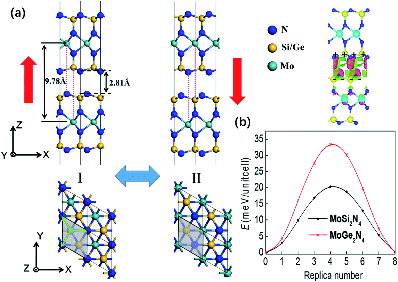 | ||
| Fig. 1 (a) Geometric structures of bilayer MoSi2N4 and MoGe2N4. I and II represent two equivalent states, where the polarization directions are marked by red arrows, the green arrow denotes the direction and distance from state I to state II upon interlayer sliding. For the interlayer differential charge density, green and red isosurfaces indicate electron depletion and accumulation after layer stacking, respectively. (b) The ferroelectric switching pathways of bilayer MoSi2N4 and MoGe2N4. | ||
It is the similar case for AB stacking MoGe2N4 bilayer. The calculated vertical polarizations are 3.36 pC m−1 and 3.05 pC m−1 for MoSi2N4 and MoGe2N4, and 2.49 pC m−1 and 3.44 pC m−1 for CrSi2N4 and WSi2N4, respectively. They are much higher compared with bilayer WTe2 (predicted to be ∼0.37 (ref. 17) and experimentally measured to be ∼0.23 pC m−1 (ref. 18)) and BN (∼2 pC m−1 for both predictions12 and experimental measurements14). It may be attributed to the stronger interlayer interaction, noting that its interlayer distance of 2.81 Å (the vertical distance between the N atoms of the upper and down layers at the van der Waals interface) is much smaller compared with bilayer graphene or BN (3.10–3.40 Å).12 The nudge-elastic-band23 (NEB) method is used to estimate the energy barrier of slippage-induced polarization switching, which turns out to be respectively 20.20 and 33.23 meV per unit cell for MoSi2N4 and MoGe2N4 bilayer, as shown by the pathways in Fig. 1(b). Those values can also be obtained in the dependence of energy on interlayer displacement along the x direction calculated in Fig. S1,† revealing typical double-well potentials for ferroelectrics.
The band structures of bilayer MoSi2N4 and MoGe2N4 in Fig. 2(a) are computed by using the Heyd–Scuseria–Ernzerhof (HSE) hybrid functional,24 revealing an indirect band gap of 2.10 eV for MoSi2N4 and 0.98 eV for MoGe2N4, within the desirable ranges for transistors. Meanwhile the electron mobility can reach 7990 cm2 V−1 s−1 according to our calculations in Table S1.† Such combination of non-volatile memories with high-mobility semiconductor transistors may enable computing-in-memory architecture where logic and arithmetic operations are performed in memory, which can greatly reduce energy cost associated with data transfer.25 The vertical polarization due to interlayer inequivalence also gives rise to the interlayer difference of distribution in band structures, splitting the bands of two layers by around 0.2–0.3 eV that should be degenerate in energy without such polarization. As shown in Fig. 2(b), the valence band maximum (VBM) is distributed in the down layer while the conduction band minimum (CBM) is distributed in the upper layer (majorly around Mo atoms in the center). The partial projected density of states (PDOS) in Fig. 2(c) reveals that the bands closest to the Fermi level are mainly distributed by the dz2 orbital of Mo atoms and the pz orbital of N atoms, where the splitting of the PDOS distributed by the two layers (see the splitting between N1 and N2, Mo1 and Mo2) is clearly displayed.
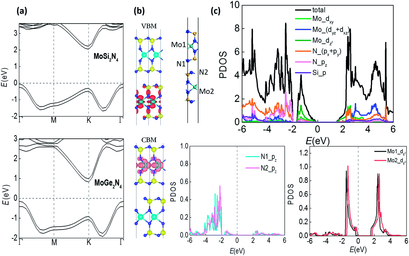 | ||
| Fig. 2 (a) Band structures of bilayer MoSi2N4 and MoGe2N4. (b) Distributions of valence band maximum (VBM) and conduction band minimum (CBM) bands, and (c) PDOS analysis for bilayer MoSi2N4. | ||
The distribution of the VBM and the CBM in Fig. 2(b) is distinct from most bilayer structures with considerable interlayer hybridizations. Taking the band structure of bilayer MoS2 in Fig. 3(a) as an example, for the non-polar AA′ stacking phase, VBM and CBM are distributed at both layers, indicating interlayer hybridizations. It is the similar case for the VBM of the polar AB stacking phase, while its CBM is mainly distributed at the down layer due to its weak vertical polarization (predicted to be 0.97 pC m−1),12 where the band splitting due to its polarization is only 0.049 eV. In comparison, the large splitting of bands (0.2–0.3 eV in Fig. 2(a)) in MoSi2N4 bilayer is induced by the vertical polarization while the interlayer hybridization is trivial according to the distribution of the VBM and the CBM in Fig. 2(b). For 2D semiconducting bilayer with a small twist angle, the internal stacking translation u(r) varying gently with position r can control the local bandgap Eg(u(r)).26 Its Moiré potential was mainly induced by interlayer coupling and estimated to be in the order of tens of meV's in hetero-bilayers like MoSe2/WS2, MoSe2/MoS2 and MoTe2/MoSe2.27 For twisted MoSi2N4 bilayer, however, the origin of Moiré potential will be the vertical polarization that induces the large band splitting instead of interlayer hybridization. The band alignments of different stacking regions are displayed in Fig. 3(b), indicating a quantum dot array with type-II heterojunctions (both in-plane and out-of-plane) that can greatly facilitate exciton trapping.
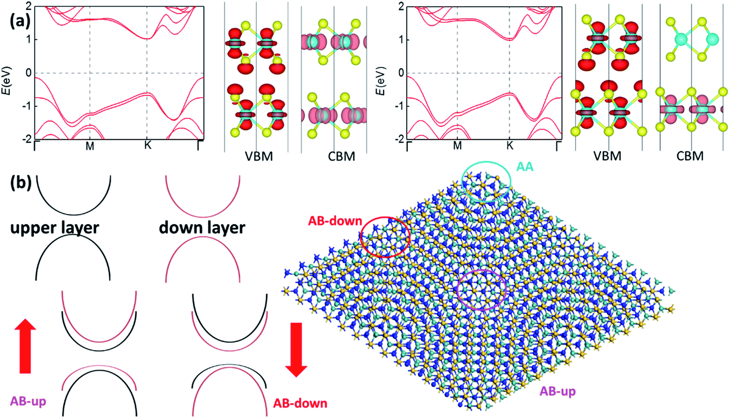 | ||
| Fig. 3 (a) Band structures of AA′ (left) and AB (right) stacking MoS2 bilayer, and their distributions of VBM and CBM bands. (b) Band alignments of different stacking regions in the Moiré superlattice of twisted MoSi2N4 bilayer. | ||
The ferroelectric phases for MoSi2N4 and MoGe2N4 multilayers with a higher thickness will be ABC stacking. For ABC-stacked MoSi2N4 and MoGe2N4 multilayers, Fig. 4(a) shows the increasing trend in polarizations and declining trend in bandgaps with increasing number of layers. Compared with bilayer MoSi2N4, the areal polarization is almost enhanced by 8 times while the bandgap decreases by almost half for six-layer MoSi2N4. We also note that MoSi2N4 monolayer was fabricated based on metallic MoN2 monolayer, which can also be used as a van der Waals electrical contact.28 It is noteworthy that the lattice mismatch between MoN2 and MoSi2N4 is similar compared with the mismatch between graphene and BN monolayer (∼2%), while the commensurate phase of graphene on BN with perfectly matching lattice constants has already been experimentally confirmed.29,30 Similar commensurate phase for MoN2/MoSi2N4 heterobilayer is likely to be formed, as shown in Fig. 4(b), where the charge on metallic MoN2 monolayer will depend on the stacking configurations with distinct polarizations. To our Bader charge analysis, the difference of the charge on the MoN2 monolayer between AB1 and AB2 stacking configurations will be as high as 0.0413e per unitcell. If the metallic MoN2 monolayer is dragged along an in-plane direction, the interlayer voltage will oscillate and an alternating current output signal will be generated, which can be used as a nanogenerator. By a coarse estimation using the formula 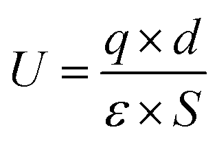 , the alternating voltage will be around 1.6 V, almost 8 times higher compared with the previous design of the nanogenerator based on C/BN hetero-bilayer,12 which can greatly facilitate driving the flow of electrons and harvest energies.31–33
 | ||
| Fig. 4 (a) The dependences of polarizations and bandgaps of ABC stacking MoSi2N4 and MoGe2N4 thin-layers on the thickness. (b) Different stacking configurations of MoN2/MoSi2N4 hetero-bilayer with distinct interlayer potentials, which can be utilized as nanogenerators. | ||
Conclusion
In summary, through first-principles calculations we show the existence of strong interlayer sliding ferroelectricity in semiconducting MoA2N4 (A = Si or Ge) bilayers and multilayers, which may enable efficient computing-in-memory. They possess the current highest vertical polarizations in sliding ferroelectrics due to strong interlayer van der Waals interactions, while giving rise to intriguing band alignments with negligible interlayer hybridizations. The twisted MoA2N4 bilayer with strong Moiré potential can be deemed as a quantum dot array with both in-plane and out-of-plane type-II heterojunctions that can greatly facilitate exciton trapping. In addition, MoN2/MoSi2N4 hetero-bilayer can be utilized as an efficient nanogenerator, suggesting promising potentials for energy harvesting.Methods
Our calculations were performed based on density functional theory (DFT) methods implemented in the Vienna Ab initio Simulation Package (VASP 5.4.4) code.34,35 The generalized gradient approximation (GGA) in the Perdew–Burke–Ernzerhof (PBE)36 exchange-correlation functional and the projector augmented wave (PAW)37 formalism were adopted. The kinetic energy cutoff was set at 500 eV. For the geometry optimization, PBE-D2 method of Grimme was used to take vdW interaction into account,38 and the Brillouin zone was sampled by a Γ-centered 9 × 9 × 1 k points using the Monkhorst–Pack scheme.39 All systems were fully relaxed, the convergence threshold for self-consistent-field iteration was set to be 10−6 eV and the atomic positions were fully optimized until the forces on all atoms are less than 0.01 eV Å−1. A vacuum space of 20 Å was set in the vertical direction. The Berry phase method was employed to evaluate the polarizations of the thin film MoSi2N4 and MoGe2N4.40Conflicts of interest
There are no conflicts to declare.Acknowledgements
The work was supported by the National Natural Science Foundation of China (No. 21573084). We thank Prof. Wei Ji for helpful discussions.Notes and references
- M. Wu and P. Jena, Wiley Interdiscip. Rev.: Comput. Mol. Sci., 2018, 8, e1365 Search PubMed.
- M. Wu and X. C. Zeng, Nano Lett., 2016, 16, 3236–3241 Search PubMed.
- Y. Bao, P. Song, Y. Liu, Z. Chen, M. Zhu, I. Abdelwahab, J. Su, W. Fu, X. Chi, W. Yu, W. Liu, X. Zhao, Q. H. Xu, M. Yang and K. P. Loh, Nano Lett., 2019, 19, 5109–5117 Search PubMed.
- K. Chang, J. Liu, H. Lin, N. Wang, K. Zhao, A. Zhang, F. Jin, Y. Zhong, X. Hu, W. Duan, Q. Zhang, L. Fu, Q.-K. Xue, X. Chen and S.-H. Ji, Science, 2016, 353, 274 Search PubMed.
- P. Sutter, H. P. Komsa, H. Lu, A. Gruverman and E. Sutter, Nano Today, 2021, 37, 101082 Search PubMed.
- N. Higashitarumizu, H. Kawamoto, C.-J. Lee, B.-H. Lin, F.-H. Chu, I. Yonemori, T. Nishimura, K. Wakabayashi, W.-H. Chang and K. Nagashio, Nat. Commun., 2020, 11, 2428 Search PubMed.
- C. Zheng, L. Yu, L. Zhu, J. L. Collins, D. Kim, Y. Lou, C. Xu, M. Li, Z. Wei, Y. Zhang, M. T. Edmonds, S. Li, J. Seidel, Y. Zhu, J. Z. Liu, W.-X. Tang and M. S. Fuhrer, Sci. Adv., 2018, 4, eaar7720 Search PubMed.
- W. Ding, J. Zhu, Z. Wang, Y. Gao, D. Xiao, Y. Gu, Z. Zhang and W. Zhu, Nat. Commun., 2017, 8, 14956 Search PubMed.
- T. Ghosh, M. Samanta, A. Vasdev, K. Dolui, J. Ghatak, T. Das, G. Sheet and K. Biswas, Nano Lett., 2019, 19, 5703–5709 Search PubMed.
- M. Wu and X. C. Zeng, Nano Lett., 2017, 17, 6309–6314 Search PubMed.
- F. Liu, L. You, K. L. Seyler, X. Li, P. Yu, J. Lin, X. Wang, J. Zhou, H. Wang, H. He, S. T. Pantelides, W. Zhou, P. Sharma, X. Xu, P. M. Ajayan, J. Wang and Z. Liu, Nat. Commun., 2016, 7, 12357 Search PubMed.
- L. Li and M. Wu, ACS Nano, 2017, 11, 6382–6388 Search PubMed.
- T. Zhong and M. Wu, Acta Phys. Sin., 2020, 69, 217707 Search PubMed.
- K. Yasuda, X. Wang, K. Watanabe, T. Taniguchi and P. Jarillo-Herrero, 2020, arXiv preprint arXiv:2010.06600.
- M. Vizner Stern, Y. Waschitz, W. Cao, I. Nevo, K. Watanabe, T. Taniguchi, E. Sela, M. Urbakh, O. Hod and M. Ben Shalom, 2020, arXiv e-prints, arXiv:2010.05182.
- P. Sharma, F.-X. Xiang, D.-F. Shao, D. Zhang, E. Y. Tsymbal, A. R. Hamilton and J. Seidel, Sci. Adv., 2019, 5, eaax5080 Search PubMed.
- Q. Yang, M. Wu and J. Li, J. Phys. Chem. Lett., 2018, 9, 7160–7164 Search PubMed.
- Z. Fei, W. Zhao, T. A. Palomaki, B. Sun, M. K. Miller, Z. Zhao, J. Yan, X. Xu and D. H. Cobden, Nature, 2018, 560, 336–339 Search PubMed.
- J. Xiao, Y. Wang, H. Wang, C. D. Pemmaraju, S. Q. Wang, P. Muscher, E. J. Sie, C. M. Nyby, T. P. Devereaux, X. F. Qian, X. Zhang and A. M. Lindenberg, Nat. Phys., 2020, 16, 1028 Search PubMed.
- Y.-L. Hong, Z. Liu, L. Wang, T. Zhou, W. Ma, C. Xu, S. Feng, L. Chen, M.-L. Chen and D.-M. Sun, Science, 2020, 369, 670–674 Search PubMed.
- H. Zhong, W. Xiong, P. Lv, J. Yu and S. Yuan, Phys. Rev. B: Condens. Matter Mater. Phys., 2021, 103, 085124 Search PubMed.
- L. Wang, Y. Shi, M. Liu, A. Zhang, Y.-L. Hong, R. Li, Q. Gao, M. Chen, W. Ren, H.-M. Cheng, Y. Li and X.-Q. Chen, Nat. Commun., 2021, 12, 2361 Search PubMed.
- G. Henkelman, B. P. Uberuaga and H. Jónsson, J. Chem. Phys., 2000, 113, 9901–9904 Search PubMed.
- J. Heyd, G. E. Scuseria and M. Ernzerhof, J. Chem. Phys., 2003, 118, 8207–8215 Search PubMed.
- M. Si, A. K. Saha, S. Gao, G. Qiu, J. Qin, Y. Duan, J. Jian, C. Niu, H. Wang, W. Wu, S. K. Gupta and P. D. Ye, Nat. Electron., 2019, 2, 580–586 Search PubMed.
- M. Wu, X. Qian and J. Li, Nano Lett., 2014, 14, 5350–5357 Search PubMed.
- D. A. Ruiz-Tijerina and V. I. Fal'ko, Phys. Rev. B: Condens. Matter Mater. Phys., 2019, 99, 125424 Search PubMed.
- L. Cao, G. Zhou, Q. Wang, L. K. Ang and Y. S. Ang, Appl. Phys. Lett., 2021, 118, 013106 Search PubMed.
- C. R. Woods, L. Britnell, A. Eckmann, R. S. Ma, J. C. Lu, H. M. Guo, X. Lin, G. L. Yu, Y. Cao, R. V. Gorbachev, A. V. Kretinin, J. Park, L. A. Ponomarenko, M. I. Katsnelson, Y. N. Gornostyrev, K. Watanabe, T. Taniguchi, C. Casiraghi, H. J. Gao, A. K. Geim and K. S. Novoselov, Nat. Phys., 2014, 10, 451–456 Search PubMed.
- M. Yankowitz, K. Watanabe, T. Taniguchi, P. San-Jose and B. J. LeRoy, Nat. Commun., 2016, 7, 13168 Search PubMed.
- F.-R. Fan, Z.-Q. Tian and Z. Lin Wang, Nano Energy, 2012, 1, 328–334 Search PubMed.
- L. Zhang, B. Zhang, J. Chen, L. Jin, W. Deng, J. Tang, H. Zhang, H. Pan, M. Zhu, W. Yang and Z. L. Wang, Adv. Mater., 2016, 28, 1650–1656 Search PubMed.
- W. Yang, J. Chen, G. Zhu, J. Yang, P. Bai, Y. Su, Q. Jing, X. Cao and Z. L. Wang, ACS Nano, 2013, 7, 11317–11324 Search PubMed.
- G. Kresse and J. Furthmüller, Comput. Mater. Sci., 1996, 6, 15–50 Search PubMed.
- G. Kresse and J. Furthmüller, Phys. Rev. B: Condens. Matter Mater. Phys., 1996, 54, 11169 Search PubMed.
- J. P. Perdew, K. Burke and M. Ernzerhof, Phys. Rev. Lett., 1996, 77, 3865 Search PubMed.
- P. E. Blochl, Phys. Rev. B: Condens. Matter Mater. Phys., 1994, 50, 17953–17979 Search PubMed.
- S. Grimme, J. Comput. Chem., 2006, 27, 1787–1799 Search PubMed.
- H. J. Monkhorst and J. D. Pack, Phys. Rev. B: Solid State, 1976, 13, 5188–5192 Search PubMed.
- R. D. King-Smith and D. Vanderbilt, Phys. Rev. B: Condens. Matter Mater. Phys., 1993, 47, 1651–1654 Search PubMed.
Footnote |
| † Electronic supplementary information (ESI) available. See DOI: 10.1039/d1ta02645c |
| This journal is © The Royal Society of Chemistry 2021 |