
 Open Access Article
 This Open Access Article is licensed under a
 Creative Commons Attribution 3.0 Unported Licence
Colloidal quantum dots and metal halide perovskite hybridization for solar cell stability and performance enhancement
Dong
Yan
ab,
Mengxia
Liu
*c,
Zhe
Li
 *b and
Bo
Hou
*d
*b and
Bo
Hou
*d
aGuangdong-Hong Kong-Macao Joint Laboratory for Intelligent Micro-Nano Optoelectronic Technology, Foshan University, 528225, P. R. China
bSchool of Engineering and Materials Science, Queen Mary University of London, London, E1 4NS, UK. E-mail: zhe.li@qmul.ac.uk
cOptoelectronics Group, Cavendish Laboratory, University of Cambridge, Cambridge, CB3 0HE, UK. E-mail: ml896@cam.ac.uk
dSchool of Physics and Astronomy, Cardiff University, Cardiff, Wales CF24 3AA, UK. E-mail: houb6@cardiff.ac.uk
First published on 18th June 2021
Abstract
Metal halide perovskites and colloidal quantum dots (QDs) are two emerging classes of photoactive materials that have attracted considerable attention for next-generation high-performance solution-processed solar cells. In particular, the hybridization of these two types of materials has recently demonstrated remarkable performance enhancement due to the complementary nature of the two constituents. In this review, we will highlight the recent progress of QDs and perovskite hybridization in solar cell applications. More specifically, the unique properties of monophase perovskite QDs will be summarised, and are demonstrated by homogeneously hybridizing perovskite QDs into the perovskite lattice. We also discuss the recent progress in heterogeneously hybridizing discrete colloidal QDs into perovskite layers which results in significant enhancement in perovskite film stability as well as corresponding solar cell performance improvement. PbS QDs, other chalcogenide QDs, and emerging two-dimensional QDs are further accounted through multiple methods, such as constructing bilayer architectures and core–shell structures or blending multiple QDs into perovskite layers. In the end, an outlook perspective of this field has been proposed to point out several challenges and possible solutions.
 Dong Yan | Dr Dong Yan is currently a visiting research scholar in the School of Engineering and Materials Science at Queen Mary University of London, UK. She obtained her PhD degree from the Institute of Microelectronics, Chinese Academy of Sciences in 2016. She then worked as a lecturer at the School of Physics and Optoelectronic Engineering, Foshan University, China. Her research interests include stability study of solution-processed cells and device characterization. |
 Mengxia Liu | Dr Mengxia Liu is a post-doctoral fellow in the Cavendish Laboratory at the University of Cambridge. She received her BSc degree in Materials Science and Engineering from Tianjin University in 2014 and her PhD degree in Electrical and Computer Engineering from the University of Toronto in 2018. Mengxia was selected as an MIT EECS Rising Star in 2018. She is a recipient of the 2019 Marie Skłodowska-Curie Actions Seal of Excellence Award and the 2018 Chinese Government Award for Outstanding Self-Financed Students Abroad. She is currently a Review Editor for the Frontiers in Energy Research. |
 Zhe Li | Dr Zhe Li is a Senior Lecturer in Materials Science at the School of Engineering and Materials Science, Queen Mary University of London. He received his PhD from Cavendish Laboratory at the University of Cambridge in 2012, and worked as a research associate/research fellow/junior group leader at Imperial College London (2012–2015) and Swansea University (2015–2017) and as a Lecturer of Energy Materials at School of Engineering, Cardiff University (2018–2019). His main research interest includes organic, perovskite and quantum dot photovoltaic cells, including emerging target applications, stability analysis and advanced material and device characterisation. |
 Bo Hou | Dr Bo Hou is a Lecturer in the School of Physics and Astronomy, at Cardiff University. He received his PhD degree from the University of Bristol (2010–2014). He worked as a postdoctoral researcher at the University of Oxford (2014–2018, Wolfson College) and a Senior Research Fellow at the University of Cambridge (2018–2020, St Edmund's College). His research interests include QD synthesis, QD solar cells, QD optoelectronics, electron microscopy (TEM) and dynamic charge transfer analysis in energy devices. |
1. Introduction
Organic/inorganic halide perovskites have shown their potential to compete with the existing photovoltaic technologies, with a certified efficiency higher than 26%.1 The high efficiency and performance of perovskite solar cells (PSCs) are supported by material properties such as a high optical absorption coefficient (105 cm−1), a long-range carrier diffusion length (1 μm), suppressed recombination (defect tolerance), well-balanced charge transfer and so on.2–7 However, the most challenging issue for the further commercialization of PSCs is the poor chemical stability of their performance under severe environments (e.g. humidity, light soaking, etc.).8–11 In recent years, several routes12 have been explored to enhance the stability of PSCs, such as compositional engineering,13 additive and passivation strategies,14–17 shape engineering,18 introducing other robust functional layers, encapsulation techniques, and device structure engineering19 by using two-dimensional (2D) and 2D/3D perovskites.11Among these, the integration of perovskites and colloidal quantum dots (QDs) into a single device appears to be an efficient approach for stability and device performance enhancement. QDs have received enormous attention because of their excellent properties emerging from quantum confinement. They offer a high versatility with an easily tunable bandgap, high quantum efficiency, high colour purity, and generally better stability than organic chromophores.20–28 One of the main fields of research and development is photovoltaics, which has demonstrated certified photovoltaic conversion efficiencies (lead sulfide, PbS QDs) as high as 13.8%.29–31 The integration combines the advantageous properties of both materials, leading to increased short circuit current due to the extended light absorption from both QDs and perovskites, enhanced stability due to the passivation of the QD surface, and a high open-circuit voltage and fill factor in the case of perovskite solar cells. In addition, low-cost solution processability at low temperatures also allows easy integration of QDs and perovskites.
It has been reported that multiple methods, such as constructing bilayer architectures32 and core–shell structures33,34 or blending one or several kinds of QDs into perovskite layers,35 were utilized for the hybridization of QDs and perovskites. Hybridization devices such as solar cells, light-emitting diodes36,37 and photodetectors38–40 have been made with improved stability and performances so far. In this review, we summarise the intensive research efforts from the aspect of QDs and metal halide perovskite hybridization in solar cells, including (I) homogeneous hybridization: perovskite QD (PQD) hybrids into perovskite films and (II) heterogeneous hybridization: PbS or other QD hybrids into perovskite films.
2. Homogeneous hybridization – PQD hybrids into perovskite films
2.1 Advantages of homogeneous hybridization
PQDs have been extensively explored due to their excellent photophysical properties and broad application prospects.41–44 PQDs have a great potential for interface engineering in PSCs due to their tunable energy bands, high photoluminescence quantum yields and low excitation energy.45–48 In terms of their same crystal structure (cubic ABX3), and similar lattice parameters, chemical composition and processing requirements, the integration of PQDs with perovskite thin films has unique advantages over other additives like polymers and molecular species.15,49Dispersing PQDs into perovskite bulk thin films is considered as a simple and efficient strategy to passivate the grain boundaries and enhance the crystallinity of the perovskite absorber layer, passivate defects in the bulk or at the surface, as well as tune the interface structure and energetics.50–53 Furthermore, the unique optical properties, especially the photoluminescence (PL) of PQDs, can be used to increase the absorption range of PSCs. In this section, we will focus on how different hybridizations have improved bulk thin film-based PSC stability and performances through its unique optical properties and interface engineering.54–57
2.2 Organic–inorganic PQDs in perovskite bulk films
PQDs are utilized as an interface modifier for perovskite bulk thin films in order to enhance band energy alignment and device integration.56,58,59 One of the earliest examples was reported by Cha et al., using a MAPbBr0.9I2.1 QD layer sandwiched between the MAPbI3 bulk thin film and Spiro-OMeTAD hole-transporting material (HTM) layer (Fig. 1a).56 As shown in Fig. 1b, by changing the Br/I ratio, the MAPbBr3−xIx QDs showed tunable energy levels. Interface engineering with the MAPbBr0.9I2.1 QDs provided appropriate band energy alignment and facilitated the hole transfer, resulting in significant improvements of fill factor, short-circuit photocurrent and power conversion efficiency (PCE) (13.32%), which shows 29% increase compared with the PQD-free case.56 This suggested a promising means for interface engineering towards efficient charge carrier extraction and hence high photovoltaic performance. However, the stability of PSCs with and without MAPbBr0.9I2.1 QDs didn't show much difference.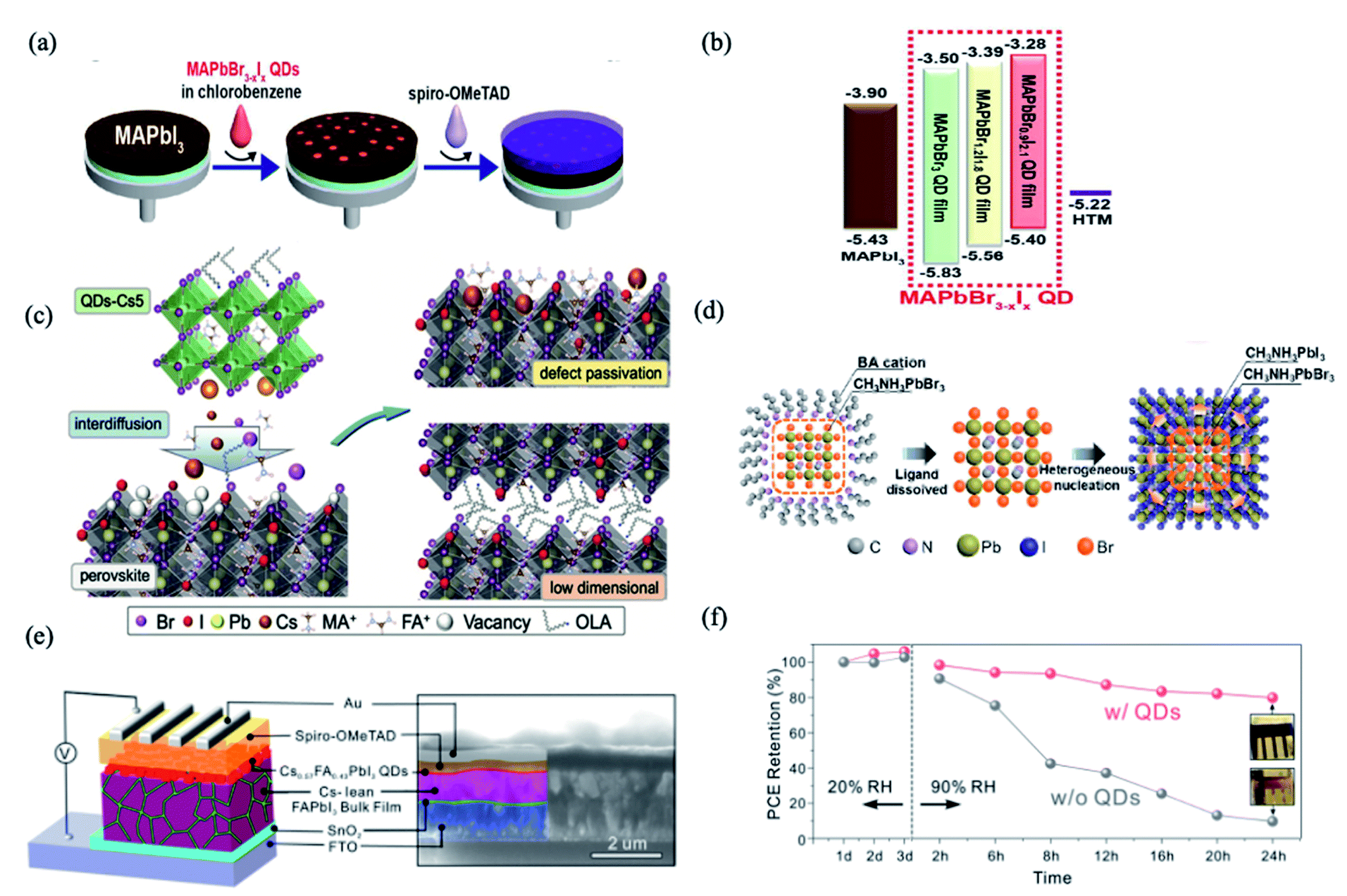 | ||
| Fig. 1 (a) Schematic illustration of fabrication procedures of the perovskite solar cells with MAPbBr3−xIx QDs. (b) Energy diagram of each material in the perovskite solar cell device with energy levels given in eV. Images are reproduced from ref. 56 with permission from the American Chemical Society. (c) Schematic of the proposed ionic defect passivation mechanism achieved through QDs-Cs modification. Images are reproduced from ref. 59 with permission from Wiley-VCH GmbH. (d) Speculative mechanism of nucleation and growth of MAPbI3 films based on MAPbBr3 QDs. Images are reproduced from ref. 60 with permission from the American Chemical Society. (e) Schematic illustration of the PSC device structure (left) and cross-sectional SEM image of the actual device (right) with the different layers indicated by false-coloring. (f) PCE evolution of PSCs with and without QD modification after storage under ambient conditions. Inset: photographs of corresponding devices after storage for 24 h. Images are reproduced from ref. 61 with permission from the American Chemical Society. | ||
The interdiffusion of PQDs into perovskite films can reduce ionic defects at the surface and grain boundaries.59 Multi-cation hybrid halide perovskite QDs, namely Csx(MA0.17FA0.83)1−xPbBr3 (abbreviated as QDs-Cs5), were dispersed in anhydrous hexane and integrated into (FAPbI3)x(MAPbBr3)1−x films.59 In this work, the composition of Cs-incorporated multi-cation PQDs was found to influence the effectiveness of ionic defect passivation. The solid-state interdiffusion process leads to the passivation of imperfections and the enhancement of photovoltaic performance characteristics observed upon treating the solar cells with QDs-Cs5. This boosted the PCE of organic–inorganic halide PSCs exceeding 21%, which retained more than 90% of their initial PCE despite exposure to continuous illumination for more than 550 h.59
PQDs are also used as nucleation sites to facilitate the growth of perovskite films. MAPbBr3 QDs with an average diameter of 4.9 nm were successfully prepared using a short alkyl ligand of n-butyl amine and dispersed in an antisolvent as nucleation centers for the growth of MAPbI3 films, as shown in Fig. 1c.60 The heterogeneous nucleation based on high lattice matching (5.5% at (110) crystalline plane) and the low free-energy barrier significantly improve the crystallinity of MAPbI3 films with decreased grain sizes (Fig. 1d), resulting in a longer carrier lifetime and lower trap-state density in the films. Meanwhile, the derived “perovskite light-emitting solar cells” with the p–i–n structure exhibit improved electroluminescence and current efficiency when operating as LEDs, and enhanced photovoltaic characteristics and stability as solar cells. The current efficiency is enhanced by an order of magnitude as LEDs, and meanwhile the PCE increases from 14.49% to 17.10% as SCs, compared to the reference device without QDs.60
Besides the above-mentioned blending approaches, constructing bilayer or multilayer structures is also a homogeneous hybridization strategy for improved efficiency and stability in PQD solar cells. Que et al. demonstrated a method that entails solution-deposition of high-Cs-content Cs1−xFAxPbI3 alloy QDs onto a bulk Cs-lean FAPbI3-based thin film (Fig. 1d), which shows a PCE (reverse scan) of 20.82% with significantly reduced hysteresis.61 The QD modification approach not only improves the charge dynamics in the devices but also improves ambient stability enhancement effects for both the FAPbI3-based thin films and the associated PSCs. As shown in Fig. 1f, when increasing the RH from 20% to 90%, within only 24 h, the PCE of the QD-free device decreased by ∼90% of its initial value, while only an ∼20% decrease was observed for the QD-modified device.
For a quick overview of organic–inorganic PQDs in perovskite bulk films, the homogeneous hybridization strategy is summarised in the upper part of Table 1. PQDs are utilized as interface modifiers, nucleation sites or spectral absorption broadening components to facilitate the growth of perovskite films through blending and fabricating bilayer or multilayer structures. In most cases, the photovoltaic efficiency of PSCs improved remarkably, however, their stability didn’t see much enhancement, especially for pure MAPbI3 QDs. When the inorganic part, Cs+, is incorporated into organic–inorganic PQDs, the hybridizing strategy achieves both high efficiency and long-term stability in QD-Cs modified perovskite solar cells due to enhanced defect passivation, and more efficient charge extraction or photocarrier harvesting.
| Cell type | V oc (V) | J sc (mA cm−2) | FF | PCE (%) | Stability | Year | Ref. |
|---|---|---|---|---|---|---|---|
| Organic–inorganic perovskite QDs in perovskite films | |||||||
| FTO/TiO2/MAPbI3/MAPbBr0.9I2.1 QDs/Spiro-MeOTAD/Au | 0.948 | 19.51 | 0.72 | 13.32 | The PSC with QDs experienced a PCE drop by 17% after 25 days, while the PSC without QDs experienced a drop by 19% | 2016 | 56 |
| FTO/NiO/MAPbI3 QDs/PCBM/Ag | 1.08 | 21.1 | 0.75 | 17.10 | The PCEs of the devices with QDs = 0.01 lost ∼25% within 6 days, while the reference devices lost ∼45% | 2018 | 60 |
| ITO/PEDOT:PSS/MAPbI3 QDS/FAPbX3 QDs/C60/Ag | 0.9 | 17.4 | 0.486 | 7.59 | — | 2019 | 62 |
| FTO/TiO2/CsPbI3:FAPbI3 QDs/PTAA/MoO3/Ag | 1.22 | 17.26 | 0.74 | 15.6 | The bilayer structure devices maintain 84% of the initial PCE after 350 h in an N2 atmosphere at room temperature, whereas the α-CsPbI3 QD-based solar cells maintain 61% | 2019 | 47 |
| FTO/SnO2/Cs-lean FAPbI3/Cs0.57FA0.43PbI3 QDs/Spiro-OMeTAD/Au | 1.121 | 24.44 | 0.76 | 20.82 | Within only 24 h, the PCE of the QD-free device decreased by ∼90% of its initial value, while only a ∼20% decrease was observed for the QD-modified device (90% RH; 30 °C) | 2019 | 61 |
| ITO/TiO2/Cs0.25FA0.75PbI3:CsPbI3 QDs/Spiro-OMeTAD/MoOx/Al | 1.20 | 18.91 | 0.76 | 15.52 | Slightly improved | 2019 | 48 |
| FTO/SnO2/(FAPbI3)x(MAPbBr3)1−x/Cs0.05(MA0.17FA0.83)0.95PbBr3 QDs/Spiro-OMeTAD/Au | 1.10 | 23.82 | 80.8 | 21.10 | The modified device retains 92.8% of its initial PCE for 1050 h under a humidity of ≈60%, while the control shows a 43.5% reduction. Maximum power point tracking shows that 95% of its initial PCE was retained under continuous illumination for 560 h in N2 | 2020 | 59 |
![[thin space (1/6-em)]](https://www.rsc.org/images/entities/char_2009.gif) |
|||||||
| All-inorganic perovskite QDs in perovskite films | |||||||
| ITO/SnO2/CsPbBr3 QDs-FAMAPb(I0.85Br0.15)3/Spiro-OMeTAD/Au | 1.12 | 23.51 | 0.7796 | 20.56 | The modified devices maintained 87.6% of their initial PCE after storage in the dark over 60 days, whereas the control devices retain 74.63% of their initial values | 2017 | 63 |
| FTO/TiO2/MAPbI3/CsPbBr3 QDs/Spiro-OMeTAD/Au | 1.13 | 22.81 | 0.79 | 20.46 | The modified device maintains 90% of the initial PCE after 500 h of continuous illumination, while the PCE of the pristine PSC reduces to 74%. | 2019 | 64 |
| ITO/PTAA/MAPbI3:CsPbBrCl2 QDs/C60/BCP/Cu | 1.15 | 23.4 | 0.8 | 21.5 | The device with 0.25 wt% QDs maintained 80% of the initial PCE after 500 h of continuous illumination, whereas the PCE of the device without QDs degraded to 27% | 2019 | 51 |
| FTO/TiO2/Cs0.05(FA0.85MA0.15)0.95Pb(I0.85Br0.15)3/CsPbBr1.85I1.15QDs/Spiro-OMeTAD/Au |
1.14 | 23.35 | 0.79 | 21.14 | The PQD-modified devices retain 94% of their initial performance under continuous light irradiation over 400 h, whereas control devices retained 73%. | 2019 | 65 |
| FTO/TiO2/CsPbI2Br/CsPbI3 QDs/PTAA/Au | 1.204 | 15.25 | 0.787 | 14.45 | The PCE shows very little degradation after 3 weeks without encapsulation in dry nitrogen and oxygen atmospheres, and degraded quickly when exposed to high humidity. | 2018 | 66 |
| FTO/TiO2/CsPbI2Br/FA+ CsPbX3/FA+ QDs/PTAA/Au | 1.215 | 14.35 | 0.745 | 14.14 | — | 2018 | 67 |
| ITO/SnO2/nano-ZnO/Cs4PbI6 and γ-CsPbI3/Spiro-OMeTAD/MoO3/Ag | 1.09 | 18.84 | 0.7995 | 16.39 | The device almost retained its initial PCE under continuous illumination (AM 1.5G, 100 mW cm) in a nitrogen-filled glovebox for 500 h | 2019 | 68 |
| ITO/PTAA/FAMACs perovskite:CsPbI3 QDs/PC61BM/C60/BCP/Cu | 1.19 | 22.95 | 0.77 | 21.03 | — | 2019 | 69 |
| FTO/TiO2/0D 3D Cs4Pb(IBr)6/CsPbI3−xBrx/Spiro-OMeTAD/Au | 1.11 | 16.56 | 0.8032 | 14.77 | The PSCs based on the 0D/3D film retained 93.9% of the PCE after 60 days of storage in a nitrogen atmosphere; however, the PCE of control PSCs degrades to below 20% of the initial values within 30 days | 2020 | 70 |
2.3 All-inorganic perovskite QDs in perovskite bulk thin films
Compared with organic–inorganic perovskites, all-inorganic perovskite with Cs+ cations was thought to exhibit excellent atmospheric stability due to their intrinsically higher thermal-decomposition temperature.18,71 Besides, the narrower energy band of cubic phase CsPbX3 (X = I, Br, or Cl) perovskites contributes to higher PCE as they can absorb long-wavelength light. However, owing to the low Goldschmidt tolerance factor, the desired α-CsPbX3 perovskite can only be stable at high temperatures (>200 °C),72 limiting its applications. When decreasing the size into nanoscale QDs or nanocrystals (NCs), the phase stability of all-inorganic perovskites would be enhanced because of reduced surface strain. Furthermore, the optoelectronic properties and bandgap energy of PQDs can be fine-tuned by designing the composition, dimensional size and shape of PQDs.73 Similarly, interfacial engineering has been widely employed with all-inorganic PQDs leading to both stability and photovoltaic efficiency enhancements.51,54,64,65,69Based on the fact that FA0.85MA0.15Pb(I0.85Br0.15)3 and CsPbBr3 possess the same crystal structure and similar lattice parameters (only 7.6% lattice mismatch), Zai et al. developed an interfacial engineering method to construct hybrid perovskite heterojunction devices with CsPbBr3 QDs penetrating the perovskite precursor mixture during film growth.63 The best performance of 20.56% was achieved thanks to the more favourable energy alignment, enhanced light harvesting, and reduced carrier recombination (Fig. 2a and b).63 In another study, CsPbBr3 QDs were introduced between the perovskite/HTL interface to improve the morphology and crystallinity of MAPbI3 films.64 CsPbBr3 QDs led to the crystallization of a passivation layer of Cs1−yMAyPbI3−xBrx on top of the perovskite layer with fewer grain boundaries and lower defect density. Therefore, the authors obtained environmentally stable perovskite solar cells with 20.46% efficiency, with reduced charge recombination and facilitated charge transfer/extraction at the interfaces (Fig. 2c and d).
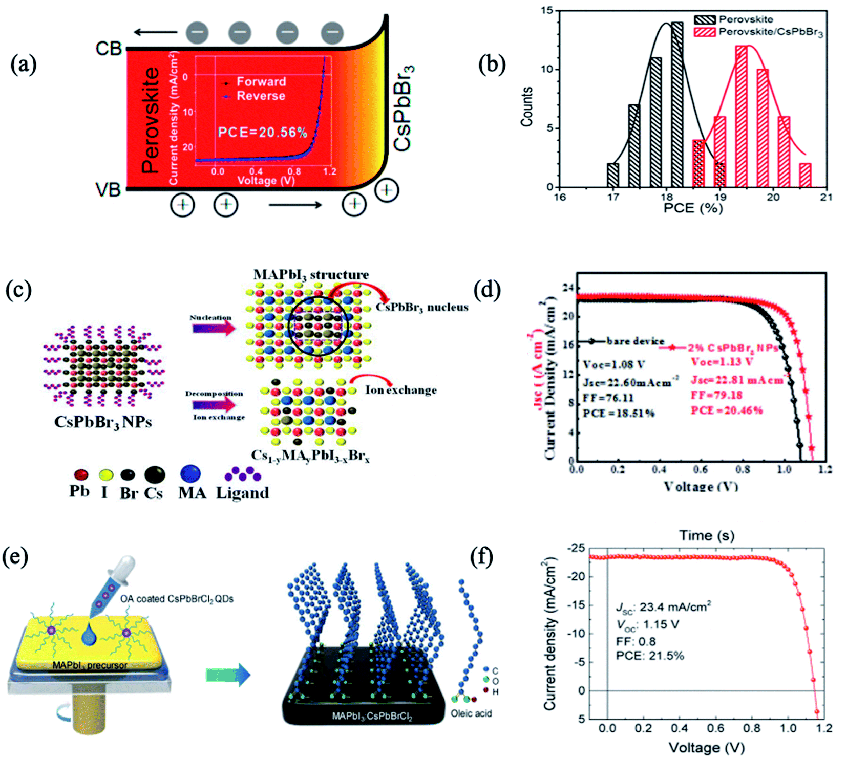 | ||
| Fig. 2 (a) Schematic diagram of the band shift of FA0.85MA0.15Pb(I0.85Br0.15)3 perovskite and CsPbBr3 NCs in a graded heterojunction structure; (inset) the highest PCE device reaching 20.56%. (b) Histogram of PCEs for 40 devices as-fabricated without and with 2 mg mL−1 CsPbBr3 NCs in chlorobenzene dripping solvent. Images are reproduced from ref. 63 with permission from the American Chemical Society. (c) Schematic nucleation and ion exchange of MAPbI3 films based on CsPbBr3 nanoparticles. (d) Current density–voltage (J–V) curves of PSCs with and without 2% CsPbBr3. Images are reproduced from ref. 64 with permission from Elsevier BV. (e) Schematic of the procedure for preparing MAPbI3 films using CsPbBrCl2 QDs. (f) J–V characteristics of the champion device with 0.25 wt% of QDs in an anti-solvent. Images are reproduced from ref. 51 with permission from Elsevier. | ||
By tuning the ratio of halide anions (I, Br, Cl and their mixtures), inorganic PQD hybrids in PSCs show a further improvement of the PCE and stability. Akin et al. incorporated an interfacial layer of inorganic CsPbBr1.85I1.15 QDs between triple-cation based perovskite and Spiro-OMeTAD layers.65 CsPbBr1.85I1.15 QDs increased the ability of hole extraction and suppressed the charge recombination by preventing the backflow of electrons, resulting in a hysteresis-free best efficiency as high as 21.14%. Moreover, PSCs with PQDs benefit from the high moisture resistivity as well as suppressed ion migration, and thus better operational stability, and retained 94% of their initial performance under continuous light irradiation over 400 h.
Besides the functional constituents for interfacial engineering layers and gradient heterojunctions in PSCs, inorganic PQDs with dopant and surface-ligand carrying vehicles are attractive for both elemental passivation and molecular surface modification. Zheng et al. utilized CsPbBrCl2 QDs as elemental dopants and molecular surface modifiers for MAPbI3 solar cells.51 When the QDs are distributed across the MAPbI3 precursor, they will decompose and leave elemental dopants inside the perovskite film and ligands on the surface of the perovskite film. The long hydrophobic alkane tails from the CsPbBrCl2 QD ligands were anchored to Pb sites on the MAPbI3 surface and retarded the moisture permeation by blocking the escape of MA cations (Fig. 2e). The PQDs passivated the defect trap states from both the bulk of active layers as well as the surface structures. Thus, this QD passivation strategy mitigated the energy disorder of MAPbI3, narrowed band-tail electronic states, and reduced mid-gap states. As a result, a CsPbBrCl2 QD-treated device yielded PCEs up to 21.5% (Fig. 2f). Under one sun of continuous illumination for 500 h, the device with 0.25 wt% QDs maintained ∼80% of the initial PCE; in contrast, the pristine device without QDs dramatically degraded to 27% of its initial PCE.51
Although organic–inorganic PSC hybrids with PQDs have achieved dramatic improvement in device efficiency, their long-term stability remains a major concern. To address this issue, extensive research efforts were dedicated to exploiting all-inorganic PSCs hybrids with all-inorganic PQDs. Bian et al. utilized a graded bandgap with the CsPbBrI2 (Eg = 1.91 eV) film under CsPbI3 (Eg = 1.77 eV and 300 nm thick) QDs as component cells, to achieve a favourable energy-level alignment for carrier collection (Fig. 3a and b).66 Optimizations including Mn2+ substitution, thiocyanate (SCN-) capping, and [(NH2)2CH]+ treatment resulted in an extended photoresponse, high carrier mobility, and well-matched energy levels, which taken together contributed to a PCE of 14.45%.66 Notably, the PCE showed very little degradation after 3 weeks without encapsulation in dry nitrogen and oxygen atmospheres. However, the black-phase CsPbI3 (α- and γ-phases) was not stable at room temperature, and it tended to convert to the nonperovskite δ-CsPbI3 phase. In another study by Bai et al., an efficient approach was described to prepare stable black-phase CsPbI3via the formation of a heterostructure consisting of 0D Cs4PbI6 and 3D CsPbI3 through tuning the stoichiometry of the precursors between CsI and PbI.68 The 0D Cs4PbI6 was suggested to surround the black-phase CsPbI3 grains to simultaneously passivate the defects and stabilize the phase stability. The corresponding PSCs with the Cs1.2PbI3.2 film can yield an impressive PCE of 16.39% with improved stability, and retained their initial PCE under continuous illumination (AM 1.5G, 100 mW cm−2, room temperature) in a nitrogen-filled glovebox for 500 h (Fig. 3c and d). All-inorganic 0D/3D Cs4Pb(IBr)6/CsPbI3−xBrx mixed-dimensional perovskite solar cells were also fabricated, by spontaneously distributing the 0D Cs4Pb(IBr)6 phase in the 3D CsPbI3−xBrx perovskite phase (Fig. 3e).70 Due to the good energy level alignment and lattice match, a 0D–3D heterojunction structure was formed. The defect passivation and non-radiative recombination suppression within the films effectively promoted carrier transport in the PSCs, boosting the PCE to 14.77%. The derived devices showed an obviously enhanced stability, retaining 93.9% of the initial efficiency after 60 days in an N2 atmosphere.
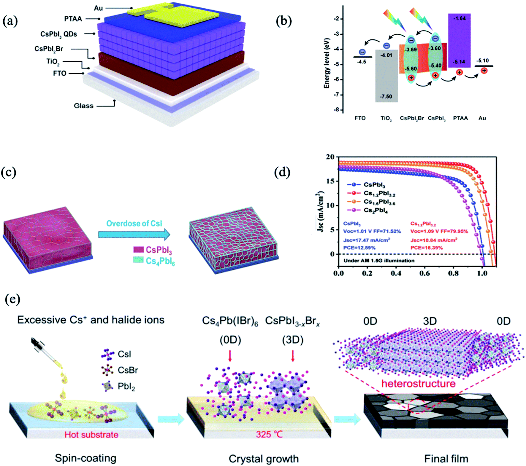 | ||
| Fig. 3 (a) Schematic structure of the device structure and energy level. (b) Energy-level diagram exhibiting the collection process of photogenerated charge carriers. Images are reproduced from ref. 66 with permission from Elsevier. (c) The structural schematic of Cs1+xPbI3+x films. (d) J–V curves of the devices using Cs1+xPbI3+x as the absorber layer. Images are reproduced from ref. 68 with permission from Wiley-Blackwell. (e) Schematic coating and formation processes of the Cs4Pb(IBr)6–CsPbI3−xBrx films. Images are reproduced from ref. 70 with permission from the Royal Society of Chemistry. | ||
Selected studies of all-inorganic PQDs homogeneous hybridization in perovskite bulk films are summarised in the lower part of Table 1. With the in-depth study and continuous optimization of the hybridization methods, as well as interfacial engineering of all-inorganic PQDs and perovskite films, the PCE and stability of PSCs have seen considerable improvement by increasing the ability of charge transfer/extraction, passivating the defect trap states, depressing ion migration or enhancing the crystallinity of the perovskite absorber layer.
3. Heterogenous hybridization
3.1 Advantages of heterogeneous hybridization
Unlike monophase PQDs, co-sensitization of perovskites and other QDs has also aroused considerable interest regarding the combination of the two material families. They show more freedom in tunability or optimization of their properties. Chalcogenide QDs are promising photovoltaic materials due to their extraordinary physical properties, such as tunable bandgaps by size control, intrinsic high extinction coefficients, and high dipole moments.74 Owing to the small lattice mismatch between the two types of materials, the integration of lead halide perovskites and lead chalcogenide QDs with various microstructures and compositions has also been used in solar cells. Particularly, PbS QDs have been likely the most widely used because of their broad light-harvesting capability to the infrared (IR) region, similar cubic crystal structures, and the relatively low lattice mismatch with perovskites.75 This section describes heterogeneous hybridization, mainly focusing on the hybridization of PbS QDs with perovskite matrixes. Some other promising chalcogenide QDs and emerging 2D QDs are also introduced.3.2 PbS QD hybrids with organic–inorganic perovskites
PbS QDs have been integrated into planar PSCs to form epitaxial interfaces such as an effective HTM with appropriate band energy alignment, and the absorption of PbS QDs also extends the whole absorption spectrum of PSCs into the infrared region.32,74,76–78 Etgar et al. reported for the first time on the use of MAPbI3 perovskite and PbS QDs in a heterojunction solar cell to obtain a panchromatic response from the visible to the IR region as it is observed from incident photon-to-electron conversion efficiency (IPCE) measurement76 (Fig. 4a). Having an appropriate band energy alignment is a crucial parameter to achieve a good performance of solar cells. By tuning the size of PbS colloidal QDs, as shown in Fig. 4b, Hu et al. engineered the energy alignment between PbS QDs acting as the HTM and the perovskite active layer, allowing the harvesting of photons with up to 1000 nm wavelength and increased significantly the performance.74 Dang et al. reported a synergistic effect of employing PbS QDs into PSCs, as they induced hydrophobic modification of the perovskite surface, leading to an improvement of the device stability in air (Fig. 4c and d).77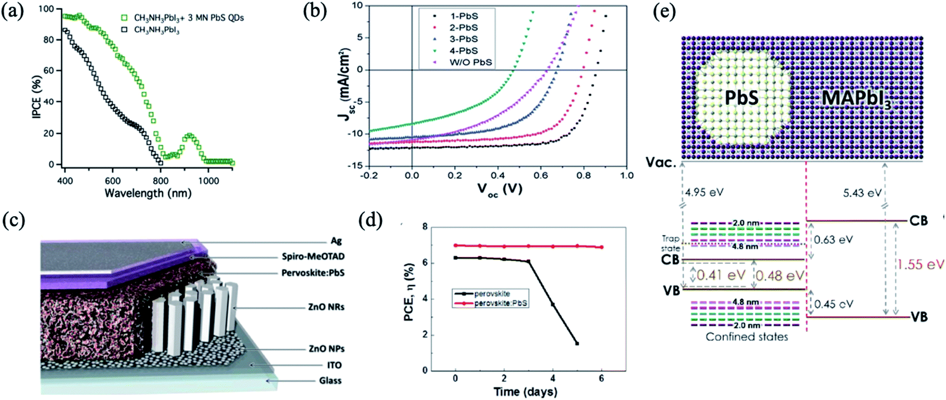 | ||
| Fig. 4 (a) The IPCE of the lead iodide perovskite heterojunction solar cell and the hybrid PbS QD lead iodide perovskite heterojunction solar cell. Images are reproduced from ref. 76 with permission from the Royal Society of Chemistry. (b) Current density–voltage characteristics of devices that employ PbS QDs of various sizes as the HTM. Images are reproduced from ref. 74 with permission from the Royal Society of Chemistry. (c) Device structure of a solar cell based on perovskite:PbS nanohybrids. (d) Efficiency variation of these perovskite and perovskite:PbS devices. Images are reproduced from ref. 77 with permission from Elsevier. (e) Band diagram of PbS in MAPbI3 used for calculations. Images are reproduced from ref. 79 with permission from the American Chemical Society. | ||
One of the critical issues on the efficiency improvement for both depleted and sensitized colloidal QD solar cells has been the passivation of surface trap states.80 The long-chain surface ligands can stabilize and control the size of colloidal QDs, however, they are also electronic barriers which compromise photogenerated carrier transport of QDs, and ultimately affect the overall performance of solar cells.81 The ligand exchange procedure opens the possibility to exchange to short ligands, improving the interdot electronic communication, and moreover passivating the trap states.
The bulky organic capping layer of colloidal QDs was exchanged by the perovskite or perovskite precursor shell. In 2014, Dirin et al. presented a general methodology for the surface functionalization of colloidal NCs with perovskites and other metal halide complexes as inorganic capping ligands, showing that MAPbI3 was the hybrid capping of PbS NCs able to retain highly efficient IR photoluminescence quantum yield.82 Seo et al. carried out perovskite passivation of PbS QDs.83 In the same year, Ning et al. produced highly concentrated quantum dot inks, using butylamine as the solvent, that can be directly deposited into thick, uniform, QD films.84 In the following year, they reported for the first time the preparation of thin films with the perovskite matrix and embedded colloidal QDs.33 Structurally, the PbS QD lattice matches well with the MAPbI3 structure both three-dimensionally (Fig. 5a) and two-dimensionally (Fig. 5b), showing less than 4.6% lattice mismatch.33 The density functional theory (DFT) calculation of an interface formation energy between PbS (100) and MAPbI3 (110) planes showed an interfacial energy less than 10 meV Å−2, suggesting that growth of MAPbI3 on PbS at room temperature is nearly homoepitaxy.33 DFT calculations further reveal that the epitaxial three-dimensional embedding of PbS QDs inside a perovskite matrix is achieved without the formation of interfacial defects. By combining the electrical transport properties of the perovskite matrix with the high radiative efficiency of the QDs, strong PL emission is achieved from PbS QDs as photogenerated electrons transfer from the perovskite to embedded QDs with an efficiency exceeding 80%. Since these early demonstrations, perovskite films with embedded QDs were applied as an active layer in different optoelectronic devices, such as solar cells,85–87 LEDs,88 and photodetectors.89
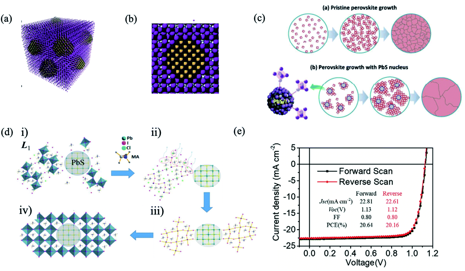 | ||
| Fig. 5 (a) Three-dimensional atomistic model of QDs in a perovskite matrix. (b) Cross-section (2D view) of a single QD in perovskite. Images are reproduced from ref. 33 with permission from Springer Nature. (c) Proposed nucleation and growth routes of perovskite crystal thin films without and with MAI-capped PbS nanoparticles. Images are reproduced from ref. 87 with permission from the Royal Society of Chemistry. (d) Schematics of the formation of MAPbI3−xClx perovskite seeded by a PbS NC, starting from (i) accelerated formation of the L1 phase by the heterointerfaces with the MAI-capped PbS NC, followed by (ii) MACl formation and sublimation. (iii) Subsequent L1-to-perovskite conversion facilitated by perovskite lattice alignment with the cubic lattice of the PbS NC. (iv) Closely packed and lattice-aligned perovskite crystals cantered around the PbS NC. Images are reproduced from ref. 90 with permission from Wiley-VCH Verlag. (e) J–V curve of the best device with forward and reverse scans. Inset table: J–V parameters of forward and reverse scans. Images are reproduced from ref. 97 with permission from Wiley-VCH Verlag. | ||
The introduction of PbS QDs into the perovskite matrix has increased the photoconversion performance of QD solar cells by the effect of QDs in the crystallization process of the perovskite layer. Recently, Gaulding et al. systematically investigated how the QD size, surface chemistry, and metal halide perovskite (MHP) film formation methods affect the resulting optoelectronic properties of QD/MHP “dot-in-matrix” systems, as shown in Fig. 4e.79 PbS acted as effective seeding sites to promote the growth of perovskite crystals, delivering substantial morphological improvements in terms of grain size, surface coverage, and uniformity. Through analyses of time-resolved crystal formation kinetics obtained from synchrotron X-rays with a fast subsecond probing time resolution, an important “catalytic” role of the seed-like PbS NCs is clearly elucidated.90 The PSC performance observed by the appropriate incorporation of PbS (Fig. 5c and d), with concentration 1.0 wt%, reached 17.4%, approximately a 25% improvement with respect to the reference devices.87 Han et al. attained a performance of 18.6% with the QD in the perovskite strategy.85 A similar effect in the grain size by QD addition has also been observed in other studies.86,91–93
The main mechanism in the ligand exchange from organic QD capping to the halide or perovskite shell is based on the binding of iodine anions to lead atoms on the QD surface.94 The sturdy and inert shell insulate the QDs from oxygen or water molecules and protect them from photocorrosion. However, agglomeration could be produced. With proper optimization of the ligand exchange process, Lan et al. introduced more iodine on the QD surface without the detrimental effect of fusion, enabling increased passivation, and enhancing the performance of QD solar cells to 10.6%.95 This strategy has been further improved using lead halide ligands, reaching a solar cell efficiency of 11.28%.96 Moreover, the passivation of lead halide also improved the stability of devices: 90% of initial efficiency was maintained after 1000 h of storage under ambient conditions.96 Yang et al. incorporated the core–shell structure of PbS/MAPbI3 QDs into a photovoltaic device with a graded band structure, achieving a better balance of open-circuit voltage (Voc) and Jsc, yielding a record solar cell performance (reaching 8.95% of PCE) using the depleted heterojunction QD solar cell configuration; however, QD solar cells strongly suffer from the hysteresis in photocurrent–voltage curves.78 More recently, Ma et al. established a multifunctional interface layer of perovskite ligand modified PbS QDs to improve the performance and stability of PSCs, reaching a high Voc of 1.13 V and FF of 80% respectively, achieving a high PCE of 20.64% (Fig. 5e).97 Moreover, the device with PbS-perovskite QDs was reported to stay nearly three times longer than the control device before its PCE decaying to 90% of its initial value under ambient conditions and continuous light soaking. They attributed the long-term stability to inhibited iodide ion mobilization, reduced defects, and increased moisture resistance ability by a more hydrophobic surface with the multifunctional interface layer. In another study reported by Masi et al., PbS QDs were used as a stabilizing agent for the FAPbI3 perovskite black phase. They developed strong bonds with the black phase FAPbI3, setting a record of concomitantly fast formation for FAPbI3 at temperatures as low as 85 °C in just 10 minutes. FAPbI3 thin films obtained through this procedure preserve the original low band gap of 1.5 eV, reach a record open-circuit voltage of 1.105 V (91% of the maximum theoretical Voc) and preserve high efficiency for more than 700 hours.93
For a quick overview of the heterogeneous hybridization of PbS QDs and perovskite bulk films, some typical reports are listed in Table 2. With an appropriate band energy alignment, PbS QDs have been integrated into planar PSCs as an effective HTM. The combination of perovskite and PbS QDs overcame the absorption limitation, resulting in a higher short-circuit current density (Jsc), compared with that for single perovskite devices with a contribution to the photocurrent of photons harvested by the two co-absorbers. PbS QDs acted as effective seeding sites to promote the growth of perovskite crystals, delivering substantial morphological improvements in terms of grain size, surface coverage, and uniformity. On the other hand, in order to reduce surface trap states, the perovskite or perovskite precursor shell acted as passivating agents and exchanged the capping layer of PbS QDs, thus increasing the photoconversion performance of QD solar cells. For comparison, in the lower part of Table 2, selected studies with heterogenous hybridization of all-inorganic perovskites with PbS QDs are shown, which will be explained in detail in Part 3.2. With the strategies of CsPbI3 shell passivated PbS QDs, multi-cation perovskites, or nano-heterojunctions, sub-bandgap trap-state assisted recombination was diminished, and the charge collection was promoted. They exhibit not only improved PCE performance but also remarkable stability.
| Cell type | V oc (V) | J sc (mA cm−2) | FF | PCE (%) | Stability | Year | Ref. |
|---|---|---|---|---|---|---|---|
| PbS QD hybrids with organic–inorganic perovskite films | |||||||
| FTO/TiO2/MAPbI3/PbS QDs/Au | 0.3438 | 24.63 | 0.43 | 3.6 | — | 2014 | 76 |
| FTO/mp-TiO2/PbS QDs:MAPbI3/P3HT/Pt | 0.88 | 6.3 | 0.493 | 4.92 | The device with PbS QDs exhibits an 18% decrease over 97 h under ambient conditions without sealing, and the control device shows a 70% decrease | 2015 | 32 |
| ITO/ZnO/PbS-MAPbI3/PbS-EDT/Au | 0.61 | 21.8 | 0.68 | 8.95 | — | 2015 | 78 |
| ITO/PbS QDs/MAPbI3/PCBM/Al | 0.86 | 12.1 | 0.72 | 7.5 | — | 2015 | 74 |
| ITO/ZnO/PbSMAI/TBAI/PbS-EDT/Au | 0.61 | 24.3 | 0.71 | 10.6 | — | 2016 | 95 |
| FTO/TiO2/MAPbI3−xClx:MAI-PbS/Spiro-OMeTAD/Au | 1.07 | 21.12 | 0.77 | 17.4 | — | 2016 | 87 |
| ITO/ZnO/MAPbI3-PbS/PbS-EDT/Au | 0.61 | 27.23 | 0.678 | 11.28 | They maintain 90% of the initial efficiency after 1000 h of storage in air, unencapsulated | 2017 | 96 |
| ITO/ZnO(NRs)/perovskite:PbS QDs/Spiro/Ag | 0.557 | 22.841 | 0.55 | 6.99 | The PCE of perovskite:PbS devices decreased by 75.7% after 5 days (from 6.3% to 1.53%), and a small decrease from 6.99% to 6.89% was observed after 6 days | 2017 | 77 |
| FTO/TiO2/TiO2-mp/MAPbI3–PbS QD/Spiro/Au | 1.028 | 23.5 | 0.772 | 18.6 | — | 2018 | 85 |
| FTO/SnO2/FAPbI3-PbS QDs/Spiro-OMeTAD/Au | 1.105 | 21.5 | 0.757 | 18 | The device with QDs preserves 85% of its performance after 720 hours, while the samples without QDs show a 30% decrease after a single day, and show no performance after 500 hours | 2019 | 93 |
| ITO/SnO2/MAPbI3/PbS QDs/PCBM & C60/Zr(acac)4/Ag | 1.12 | 22.61 | 0.80 | 20.16 | The time of PSCs with the PbS-PVSK QD interface layer decayed to 90% of the initial PCE and was extended nearly three times longer as compared to the control PCSs under ambient conditions and continuous light soaking | 2020 | 97 |
|
|||||||
| PbS QD hybrids with all-inorganic perovskite films | |||||||
| ITO/ZnO/PbS-mixed QDs/PbS-EDT/Au | 0.62 | 26.8 | 0.639 | 10.45 | The unencapsulated device retains 80% PCE after 10 days of storage in air | 2017 | 35 |
| ITO/MZO/PbS–CsPbI3–P/PbS-EDT/Au | 0.64 | 24.5 | 0.67 | 10.5 | The device maintains ≈88% of the initial efficiency after aging for ≈46 h with AM1.5G 100 mW cm−2 illumination | 2018 | 98 |
| ITO/ZnO/CsPbBrxI3−x:PbS/PbS-EDT/Au | 0.64 | 28.9 | 0.684 | 12.6 | The PSCs retain 95% of the initial PCE after 2 h of continuous AM1.5G illumination, unencapsulated, while the PCEs of matrix-free controls degrade to 70% of the initial value within an hour | 2019 | 34 |
| FTO/TiO2/CsPbI3 QDs:CsxFA1−xPb3 QDs:FAPbI3 QDs/PTAA/MoO3/Ag | 1.22 | 17.26 | 0.74 | 15.6 | In an N2 atmosphere at room temperature, the bilayer device maintains 84% of the initial PCE after 350 h of aging, whereas the controls maintain 61% of the initial values | 2019 | 47 |
3.3 PbS QD hybrids with all-inorganic perovskite films
An emerging alternative to organic–inorganic hybrid halide perovskites is the use of all-inorganic perovskites, which exhibit higher stability.71,89,98–101 It was reported that the CsPbI3 shell passivated PbS QDs diminished the sub-bandgap trap-state assisted recombination, hence improving the charge collection and allowing performance as high as 10.5%.98 In addition, colloidal QD solar cells based on PbS/CsPbI3 QDs present extremely low hysteresis, not only in different scanning directions but also in different scan sweep steps98 (Fig. 6a and b). Moreover, these devices also exhibit remarkable stability not only under continuous 1-sun illumination for 46 h, but also under ambient conditions for 42 days.98 On the other hand, Jung et al. studied theoretically the bond formation and carrier confinement at the PbS–CsPbBr3 interface. They elucidated that PbS and CsPbBr3 present just ∼0.5% lattice mismatch, much lower than the lattice mismatch between PbS and MAPbI3 (∼5%), which ensures high-quality epitaxy with low strain between PbS QDs and CsPbBr3.88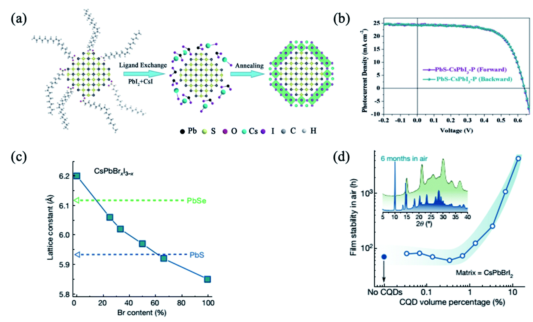 | ||
| Fig. 6 (a) Schematic illustration of the fabrication process of inorganic CsPbI3–P coating on the PbS QDs. (b) PbS–CsPbI3–P based QD solar cell with different voltage scanning directions. Images are reproduced from ref. 98 with permission from Wiley-VCH Verlag. (c) The lattice constant of lead chalcogenide QDs and caesium lead halide perovskites of different stoichiometry. (d) Stability of the lattice-anchored CsPbBrI2 perovskite with different ratios of QDs. Inset, X-ray diffraction of CsPbBrI2 films with 13 vol% QDs (green trace) and without QDs (blue trace) after being stored in air for 6 months. Images are reproduced from ref. 34 with permission from Springer Nature. | ||
Lattice mismatch can be further reduced by the use of mixed halide I–Br or Br–Cl perovskites. By tuning the ratio of Br to I in the CsPbBrxI3−x matrix composition, Liu et al. achieved near-zero lattice mismatch (ε) for PbS QDs at a Br content of approximately 66% (ε < 0.2%), enabling the strain-free epitaxial growth of perovskite (Fig. 6c). The lattice-anchored QDs:perovskite solid exhibits a photoluminescence quantum efficiency of 30 percent for a QD solid emitting at infrared wavelengths, and a doubling in charge carrier mobility as a result of a reduced energy barrier for carrier hopping compared with the pure QD solid. The film stability is improved from three days to more than six months when 13 vol% QDs are incorporated (Fig. 6d).34 Furthermore, the devices with the 15 vol% CsPbBr2I matrix exhibited the highest PCE of 12.6%, which is a reproducibly enhanced performance relative to controls. They also showed improved photostability, retaining 95% of their initial PCE under continuous AM1.5G illumination for 2 h, unencapsulated, while the PCE of controls degraded to 70% of their initial value within an hour. This is attributed to the lattice-matching perovskite matrix which provides surface passivation and lowers the energy barrier for carrier hopping.
The nano-heterojunction or contact heterojunction structure is different from the core–shell structure. Discrete nanoparticles each composed of QDs and hetero nanoparticles are combined by chemical bonding or physical contact.35,47,92,102,103 The nano-heterojunction structure may incorporate new functions beyond those of each independent component. Yang et al. devised a strategy based on n- and p-type ligands that judiciously shifted the QD band alignment.35 The best performing devices and controls were achieved using a mixture of organohalide perovskite ligand based MAPbI3 for electron acceptor (A-type) QDs, and thioglycerol for donor (D-type) dots. Interdot carrier transfer and exciton dissociation studies confirmed efficient charge separation at the nanoscale interfaces between the two classes of QDs. The first fabricated mixed-QD solar cells achieved a power conversion of 10.4%, surpassing the performance of previously reported bulk heterojunction QD devices fully two-fold35 (Fig. 7a and b). The unencapsulated device retains 80% PCE after 10 days of storage in air. In another study (Fig. 7c and d), heterostructured CsPbX3–PbS (X = Cl, Br, I) QDs were successfully synthesized via a room temperature in situ growth of PbS method by using hexamethyldisilathiane ((TMS)2S) as the sulfur precursor.103 The CsPbX3–PbS QDs exhibited dual PL peaks in visible and near infrared regions, corresponding to CsPbX3 and PbS, respectively. The femtosecond TAS study confirmed that exciton energy effectively transferred from CsPbBr3 to PbS in CsPbBr3–PbS QDs when CsPbBr3 is excited. Nano-heterojunctions containing PQDs and hetero QDs may promote the development of highly efficient photovoltaic and optoelectronic devices.
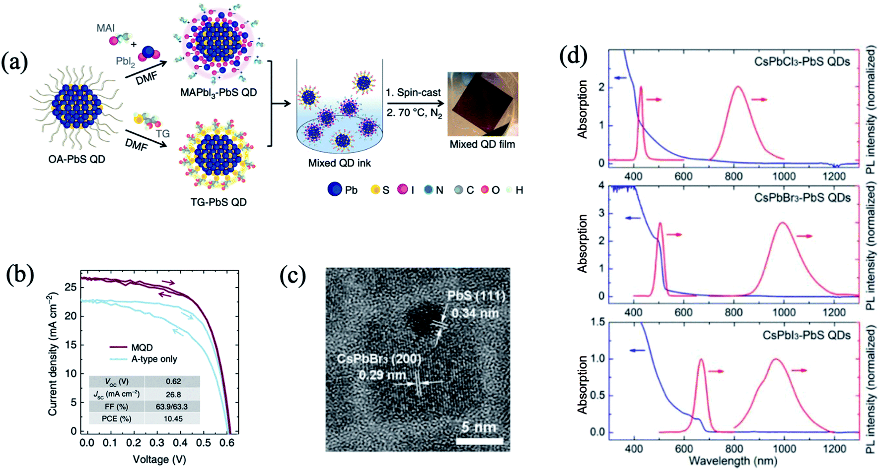 | ||
| Fig. 7 (a) Schematic of the preparation of mixed-quantum-dot solids using solution ligand exchange. (b) PCE values of mixed QD devices with different mass ratios of D- (TG-capped) and A-type (MAPbI3-capped) QDs. Images are reproduced from ref. 35 with permission from Springer Nature. (c) HRTEM image of a typical CsPbBr3–PbS QD. (d) The absorption and corresponding PL spectra of the CsPbX3–PbS (X = Cl, Br, I) QDs (λex = 325 nm). Images are reproduced from ref. 103 with permission from the American Chemical Society. | ||
3.4 Other chalcogenide QD hybrids with perovskite films
Besides PbS QDs, other chalcogenide QDs such as CdSe,102,104 CdTe,105 ZnSe,106 CdSe/ZnS or CdS/ZnS core/shell QDs,53,104 SnS,107 ZnO,14 copper indium sulphide (CIS),108 Cu12Sb4S13 (CAS),109etc. are utilized to hybridize with perovskites. CdSe/CsPbI3 QDs were used as an interface layer between the MAPbI3 perovskite film and the hole transport layer to promote interfacial charge extraction and enhance light-harvesting ability simultaneously.102 Compared with pristine PSCs, hybrid PSCs achieve 21% enhancement in PCE, which can be attributed to the ultrafast charge carrier dynamics and Förster resonance energy transfer effect (Fig. 8a and b). In Fig. 8c, it is shown that the modified devices with QDs show better stability than those without QDs, which should be attributed to the weakening of the affinity of the perovskite film to water by the QD layer.102 Hanmandlu et al. incorporated CdSe/ZnS QDs into the MAPbI3 perovskite to passivate the surface charge traps and grain boundaries.104 Based on this passivation strategy, the target devices exhibited a PCE close to 20% with suppressed hysteresis in the J–V characteristics and a fill factor of 81.44%. Moreover, they achieved long-term stability under an N2 atmosphere at 50 °C, retaining 80 and 75% of their initial PCE after 720 h and after 2400 h, respectively; in contrast, the control device lost 70% after 360 h.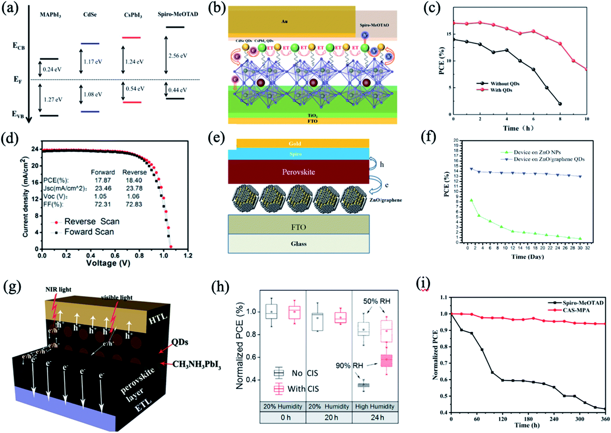 | ||
| Fig. 8 (a) Band level diagram of each layer. (b) Schematic diagram of the energy transfer (ET) and charge transfer in the device. (c) Stability of the pristine device and QD incorporated device. Images are reproduced from ref. 102 with permission from the Royal Society of Chemistry. (d) Typical J–V curves of cells with the CdTe–MAPbI3 interlayer. Images are reproduced from ref. 105 with permission from Elsevier BV. (e) Schematic images of the perovskite solar cell on the ZnO/rGO film. (f) Stability of the devices based on ZnO nanoparticles and ZnO/rGO QDs in an ambient environment after encapsulation using UV-epoxy. Images are reproduced from ref. 14 with permission from John Wiley and Sons Ltd. (g) Schematic diagram of the charge transportation process in ETL/QDs-MAPbI3 hybrid layer/HTL. Images are reproduced from ref. 107 with permission from Wiley-VCH Verlag. (h) Photovoltaic stability of perovskite solar cells with and without CIS NCs under a controlled humidity environment. Images are reproduced from ref. 108 with permission from Wiley-VCH Verlag. (i) Long-term stability of PQD SCs with Spiro-MeOTAD and CAS QDs HTMs in ambient air. Images are reproduced from ref. 109 with permission from the American Chemical Society. | ||
Similarly, with the congeneric junction contact between the perovskite and CdTe QDs, the devices with the CdTe QDs in perovskite films achieve a high efficiency (∼19.3%, averaged) with a significantly reduced hysteresis (Fig. 8d).105 The reduced hysteresis is partially contributed from faster hole extraction at the interface thanks to the high hole mobility in CdTe.
Tavakoli et al. synthesized a quasi-core shell structure of ZnO/reduced graphene oxide (rGO) QDs as an electron transfer layer (Fig. 8e).14 In this regard, rGO not only passivated the surface of ZnO nanoparticles to prevent the reaction with MAI, but also extracted the charge carriers quickly from the perovskite layer to reduce carrier recombination. The resulting PSC on the ZnO/rGO layer exhibited a stable PCE as high as 15.2% and 11.2% on fluorine-doped tin oxide (FTO) glass and polyethylene terephthalate (PET) substrates, respectively, under AM1.5G illumination. Besides, the PCE dropped only 10% after 30 days, which was much more stable than that of the pure ZnO one (90% drop) (Fig. 8f). In this case, the ZnO/rGO quasi-core shelled QDs were inserted into a layer-by-layer structure, which is considered as one type of hybrid structure in a broad sense. However, because of our review focus on direct hybridization of QDs with perovskites at the level of the materials, we will not expand more discussions for layer-by-layer hybridizations.
As an absorber layer in PSCs, SnS QDs–MAPbI3 hybrid films were fabricated by a facile in situ crystallization method, enabling easy embedding of the QDs in the perovskite layer (Fig. 8g).107 Compared with SCs based on pure MAPbI3, the champion SCs achieve a 25% enhancement in efficiency, giving rise to an efficiency of 16.8%. The improved performance can be attributed to the optimized crystallinity of the absorber, enhanced photo-induced carrier separation and transport within the absorber layer, and increased absorption intensity in the visible and NIR light region.
The incorporation of a CIS NC layer into the perovskite solar cell gave rise to enhanced hole transport and moisture stability.108 Water contact angles of perovskite films without and with CIS NCs show that CIS is more hydrophobic, and is likely to slow the rate at which moisture is able to infiltrate into the perovskite. With the protection of CIS NCs, they prevented moisture from penetration into the perovskite and acted as a moisture resistant coating.108 The derived devices exhibited superior resistance to humidity and improved photovoltaic stability after 4 h under 90% humidity without device encapsulation (Fig. 8h). In contrast, the PCE of PSCs without a CIS layer decreased significantly. Meanwhile, the CIS NC layer can modify the interface between the perovskite and hole transporting material, suppressing charge recombination pathways.
The surface oleylamine ligands of CAS QDs are exchanged with 3-mercaptopropionic acid, realizing enhanced electronic coupling and a reduced band gap.109 The all-inorganic PQD SCs with CAS QDs exhibit a PCE of 10.02%, achieving a high Jsc of 18.28 mA cm−2 because of the improved light absorption and hole extraction ability of CAS QDs. Moreover, CAS QD based PSCs exhibit enhanced long-term stability and retain 94% of their initial PCE after storage in ambient air for 360 h.
Table 3 summarises selective studies of chalcogenide QDs hybridized into PSCs. The heterogeneous hybridization of chalcogenide QDs in PSCs promoted interfacial charge transport and extraction, crystallinity of the absorber, and light-harvesting ability simultaneously, which gave rise to enhanced performance and stability. This is associated with high hole mobility, broadening absorption range, grain boundary passivation, or the weakening affinity to water by the chalcogenide QDs.
| Cell type | V oc (V) | J sc (mA cm−2) | FF | PCE (%) | Stability | Year | Ref. | |
|---|---|---|---|---|---|---|---|---|
| Other chalcogenide QD hybrids with inorganic perovskite films | ||||||||
| FTO/ZnO–graphene/MAPbI3/Spiro-OMeTAD/Au | 1.03 | 21.7 | 0.68 | 15.2 | The PCE dropped only 10% after 30 d, which was much more stable than the ZnO one (90% drop) | 2016 | 13 | |
| FTO/TiO2/CH3NH3PbI3–SnS/Spiro-OMeTAD/Au | 1.04 | 22.7 | 0.716 | 16.8 | — | 2017 | 107 | |
| FTO/TiO2/CH3NH3PbI3/CIS/Spiro-OMeTAD/Au | 1.04 | 21.8 | 0.612 | 13.8 | After 4 h under 90% humidity, the PCE decreased to 0.6 of the original normalized PCE, much higher than those of the controls without the CIS NC layer | 2017 | 108 | |
| ZnSe QDs/FTO/TiO2/MAPbI3/Spiro-OMeTAD/Au | 1.1 | 20.3 | 0.799 | 17.3 | After UV irradiation for 460 min, the solar cell without the LDS layer has lost efficiency, while the efficiency of the solar cell with the LDS layer remained at 50% of the initial value | 2018 | 106 | |
| ITO/SnO2/MAPbI3/CdTe QDs/Spiro/Ag | 1.10 | 22.42 | 0.7771 | 19.19 | — | 2018 | 105 | |
| FTO/TiO2/CH3NH3PbI3/CdSe + CsPbI3 QDs/Spiro-OMeTADAu | 0.976 | 24.6 | 0.710 | 17.1 | Compared with devices without QDs, devices with QDs show better stability | 2020 | 102 | |
| FTO/c-TiO2/m-TiO2/CsPbI3 QDs/Cu12Sb4S13 QDs/Au | 1.04 | 18.28 | 0.529 | 10.02 | The Cu12Sb4S13 based PSCs maintain 94% of their initial PCE, while the PCE of Spiro-MeOTAD based PQD SCs drops to 42% in 360 h | 2020 | 109 | |
| ITO/PEDOT:PSS/MAPbI3/CdSe–ZnS QDs/C60/BCP/Ag | 1.06 | 23.04 | 0.8144 | 19.89 | The target device lost 25% of its initial PCE after heating for 720 h at 50 °C; the control device lost 70% of its initial after 360 h. | 2020 | 104 | |
3.5 Emerging 2D QD hybrids with perovskite films
In addition to chalcogenide QDs, QDs such as carbon QDs,50,110,111 graphene QDs (GQDs),112,113 black phosphorus QDs (BPQDs),114etc., have emerged as efficient perovskite absorbers to improve the PCE and the stability of PSC devices. Ma et al. added hydroxyl and carbonyl functional group-containing carbon QDs into the perovskite precursor solution to passivate the uncoordinated Pb2+ ions in grain boundaries (Fig. 9a).50 This method decreased nonradiative recombination, leading to higher PL intensities and longer carrier lifetimes in the perovskite film. The champion device achieved a PCE of 18.24% and retained 73.4% of its initial PCE after aging for 48 h under 80% humidity in the dark at room temperature (Fig. 9b).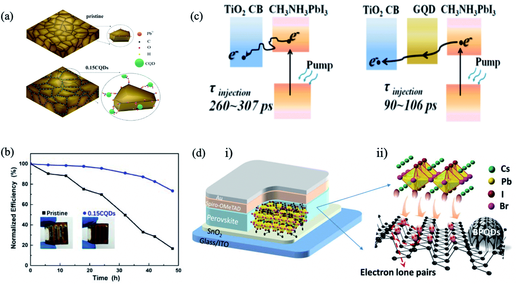 | ||
| Fig. 9 (a) Schematic diagram of the proposed mechanism of QD passivation. Pb2+, C, O, H and QDs are illustrated as orange, black, red, green and cyan, respectively. (b) The normalized PCEs against aging time measured under 80% humidity in the dark at room temperature. Images are reproduced from ref. 50 with permission from the American Chemical Society. (c) Schematics of electron generation and extraction at TiO2/perovskite and GQD/TiO2/GQD/perovskite interfaces. Images are reproduced from ref. 112 with permission from the American Chemical Society. (d) CsPbI2Br solar cell devices with different addition amounts of BPQDs. (i) Schematic structure of the device and interaction between BPQDs and CsPbI2Br: the unbonded lone pairs of BPQDs offer excess electrons and facile interaction with cationic ions in CsPbI2Br, causing the CsPbI2Br NCs formed to be attached onto BPQDs that supply effective heterogeneous nucleation sites. (ii) Schematic diagram of CsPbI2Br growth onto the BPQD surface. Images are reproduced from ref. 114 with permission from American Association for the Advancement of Science. | ||
GQDs have been another focus in the interfacial engineering of PSCs due to their high charge carrier mobility and high transmittance in the entire visible light spectrum, showing great promising for photovoltaic applications. Inserting an ultrathin layer of GQDs between the perovskite and the mesoporous titanium dioxide ETL facilitates electron transfer, leading to the boosting of the photocurrent and thus the efficiency of the corresponding solar cells.112 The graphene QDs act as a superfast electron tunnel that strongly quenches the PL of the perovskite absorber and decreases the electron extraction time from (260–307 ps) to (90–106 ps) (Fig. 9c). Zhou et al. combined graphene QDs and SnO2 in an effective ETL for high-performance flexible PSCs.113 The optimized graphene QDs/SnO2 ETL has higher electron mobility, better film coverage and better energy level alignment matching compared to the pristine SnO2, resulting in promoted charge transfer and suppressed charge recombination (Fig. 9d). Moreover, the optimized device yielded PCEs of 19.6% for the rigid substrate and 17.7% for the flexible substrate.
Recently, BPQDs are incorporated as effective nucleation sites to modulate the crystalline growth of CsPbI2Br perovskite thin layers, facilitating crystallization and film morphology.114 The lone-pair electrons of BPQDs can induce strong interaction of intermolecular combination with molecules of the CsPbI2Br precursor solution. The BPQDs@CsPbI2Br hybrid films concomitantly reinforce a stable CsPbI2Br crystallite and suppress the oxidation of BPQDs. Consequently, an impressive PCE of 15.47% was achieved for BPQDs@CsPbI2Br (0.7 wt%) hybrid film devices, with an enhanced cell stability, under ambient conditions.
2D QDs have emerged as additives for interfacial engineering to enhance both the PCE and stability of PSC devices (Table 4). Due to their unique optoelectronic properties like high charge carrier mobility and their excellent nonlinear optical properties, they result in enhanced-PL intensities, longer carrier lifetimes, larger grain boundaries, reduced non-radiative recombination and facilitated crystallization and film morphology when hybridizing in the perovskite layer. Their interaction suggested a promising route toward the future realization of efficient and stable PSCs.
| Cell type | V oc (V) | Jsc (mA cm−2) | FF | PCE (%) | Stability | Year | Ref. | ||
|---|---|---|---|---|---|---|---|---|---|
| 2D QD hybrids with perovskite films | |||||||||
| FTO/TiO2/GQDs/MAPbI3/Spiro-MeOTAD/Au | 0.937 | 17.06 | 0.635 | 10.15 | — | 2014 | 112 | ||
| FTO/TiO2/MAPbI3–carbon QDs/Spiro-OMeTAD/Au | 1.08 | 20.66 | 0.7391 | 16.49 | — | 2018 | 110 | ||
| ITO/NiOx/MAPbI3:carbon QDs/PCB61M ETL | 1.07 | 21.68 | 0.7878 | 18.24 | The PCE of the 0.15 QD device remained at 73.4% of the initial value after aging for 48 hours under 80% humidity in the dark at room temperature while the PCE of the control device degrades to 16.7% of the initial value | 2019 | 50 | ||
| FTO/graphene SnO2/CsFAMA–perovskite/Spiro/Au | 1.08 | 23.5 | 0.77 | 19.6 | The devices retain 91% of the original value after 500 bending cycles | 2019 | 113 | ||
| ITO/SnO2/BPQDs@CsPbI2Br/Spiro/Au | 1.25 | 15.86 | 0.78 | 15.47 | The hybrid device maintained 80% of its initial PCE under ambient conditions for 500 hours (28 °C, 35 to 45 RH%) in the dark, whereas the PCE of controls degraded to 50% of the initial value | 2020 | 114 | ||
4. Summary and outlook
Both QDs and perovskites are highly promising in the photovoltaic field and have achieved significant progress in a short period of time. The homogeneous and heterogeneous combination of QDs and perovskites leads to high-performance photovoltaics. On the basis of their crystal structures, the relatively low lattice mismatch promotes the crystallization of the perovskite lattice with large grains. The complimentary light-harvesting extends the absorption from visible to the NIR region with QD-enhanced light collection. Besides, the band alignment between the perovskite and QDs can also be tailored to favour efficient carrier transport and rapid extraction of charge carriers. By surface and interface engineering, the perovskite can increase the passivation of the QD surface, thus enhancing the stability.Although impressive progress has been achieved in the performance and stability of PSCs with perovskite and QD hybridization, the improvement mechanism is not clear until now. The PCE values are relatively lower than those of pure PSCs with the highest efficiency. This is associated with the material and device properties of both QDs and perovskite solar cells, as well as the lattice mismatch and energy alignment between the two material families. On the other hand, the design of the device structure is significant for performance improvement. Future studies call for a systematic exploration of interface engineering, band-structure of materials, and optimized configurations of the hybridization of QDs and perovskite. We compare and analyze the above-mentioned hybrid structures, and then we summarise the prospects of the future directions of this hybrid QDs/perovskite SC as follows in Fig. 10.
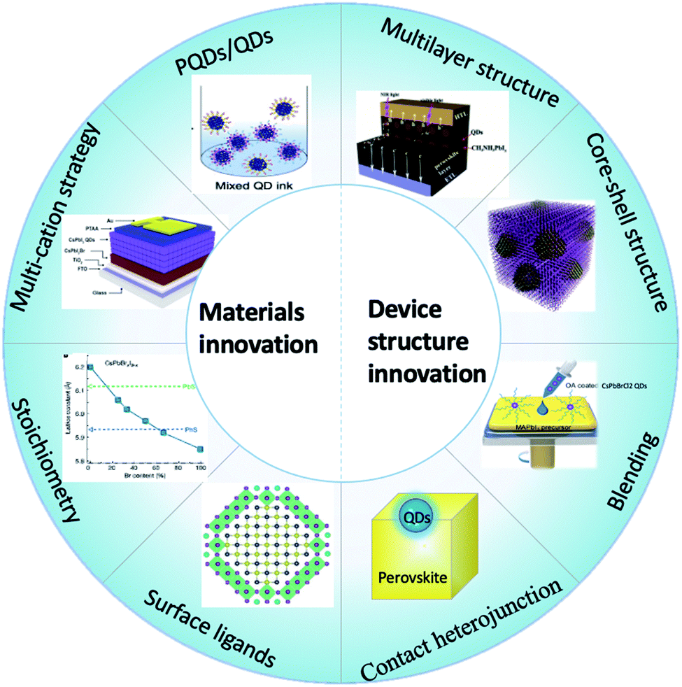 | ||
| Fig. 10 Material and device structure innovation for the hybridization of QDs and perovskites. | ||
4.1 Summary of hybrid structures
To date, there are four types of perovskite and QD heterostructures reported: (1) QD blending in the continuous perovskite matrix; (2) multilayer architectures composed of perovskites and QDs; (3) capping traditional QDs with a perovskite layer in PSCs, or a reverse structure to grow an entire shell on perovskite QDs; (4) nano-heterojunctions of perovskites and other QDs. One primary goal of introducing QDs into or on top of perovskite films was device operation related, namely to improve the device performance by enhancing energy level alignment, and efficient charge extraction and charge transport rate. In other cases, interface engineering has also been applied between the perovskite bulk film and charge transport layers for surface defect passivation, QD coupling and device performance improvements.Annealing time is a crucial parameter to determine whether the hybridizing type is blending or formation of a multilayer structure. When the QD solution was added before film annealing, it is suggested that QDs would be incorporating into the perovskite film via diffusion reaction. Otherwise, solar cells with a multilayer structure would be fabricated via layer-by-layer deposition with a multi-junction stacking technique. However, the multilayer or bilayer structures do not mean they are interaction-free at the interface. A component-graded heterojunction is formed throughout the perovskite/QD bilayer interface via interface engineering. Specifically, some of the ions in the perovskite layer are exchanged with ions from QDs, and vice versa.
The resultant influences of the interaction between QDs and the perovskite film include ligand exchange and nano heterojunctions or contact heterojunctions. The ligand exchange procedure is adopted in a core–shell structure, which can exchange to a short ligand, improve the interdot electronic communication, and thus passivate the trap states. Nano-heterojunction structures combine the two materials by chemical bonding or physical contact, and terminate the dangling bond.
When fabricating solar cells, one or more techniques could be applied at the same time. For example, a core–shell structured QD could be blended in perovskite bulk films, and also used as an interface layer to fabricate multiple layers and quantum junctions for optoelectronic applications. In Table 5, we have summarized the best PCE enhancement with homogeneous hybridization and heterogeneous hybridization in PSCs. It is worth mentioning that we didn't compare the stability here as there isn't a uniform standard for stability.
| Hybrid type | Structure type | PCE (organic–inorganic/inorganic) |
|---|---|---|
| Homogeneous hybridization | Multilayer | 21.5% (ref. 51)/14.45 (ref. 66) |
| Blending | 21.1% (ref. 59)/16.39 (ref. 68) | |
| Heterogeneous hybridization | Multilayer | 20.16% (ref. 97)/— |
| Blending | 18.6% (ref. 85)/— | |
| Core–shell structure | 20.16% (ref. 97)/— | |
| Nano-heterojunction | 15.6% (ref. 47) (QDSC) |
4.2 Materials innovation
The tunable optical and electronic properties of QDs and perovskites provide a great possibility for optimizing the hybridizations. Besides the above-mentioned hybridizations, the selection of stoichiometry in QDs, multi-cation strategies by substituting A, B or X sites in the perovskite crystal structure (ABX3), as well as optimization of surface ligands are promising to further facilitate the near-perfect interfacial lattice match for QD/perovskite heterostructures. For example, other octahedral metal hexa-halide cluster ligands, such as MA4PbI6, MA3BiI6, MA4–InCl6, and MA4MnCl6, also allow the quasi-epitaxial growth of the ligand shell.115 Moreover, the processing methods of both material families and their interfacial physics and chemistry require further in-depth study, which may offer more insights into exploring effective strategies to achieve defect-free interfaces.4.3 Device structure innovation
The homogeneous and heterogeneous hybridization of QDs and perovskites has been proved to improve the performance of optoelectronic devices based on strategies like fabricating multilayer structures and core–shell structures, blending or constructing nano-heterojunction structures. With the emergence of tandem and/or cascade junction solar cells with boosting efficiency, the solution processability of both QDs and perovskite provides promising opportunities towards applications for hybrid devices. Besides, the interaction between the perovskite and QDs also presents new properties that do not exist in single-phase materials, such as the formation of the exciplex state at lower energies than both the perovskite and QD band gap, demonstrating the potentiality for the development of advanced optoelectronic devices, such as tunable color LEDs116 or intermediate band gap solar cells.117 Continued studies on QDs- and/or perovskite-based hybridizations will undoubtedly further open up the optimization of current devices and the exploration of innovative device structures.Author contributions
D. Y. drafted the manuscript. M. X. L., Z. L. and B. H. revised the content. All authors have reviewed and given approval to the final version of the manuscript.Conflicts of interest
There are no conflicts to declare.Acknowledgements
D. Y. acknowledges the financial support from the National Natural Science Foundation of China (61704027) and the Research Fund of Guangdong-Hong Kong-Macao Joint Laboratory for Intelligent Micro-Nano Optoelectronic Technology (2020B1212030010). Z. L. acknowledges the funding from the Engineering and Physical Sciences Research Council (EP/S020748/1). B. H. would like to acknowledge the financial support from Cardiff University.References
- https://www.nrel.gov/pv/cell-efficiency.html .
- K. T. Cho, S. Paek, G. Grancini, C. Roldán-Carmona, P. Gao, Y. Lee and M. K. Nazeeruddin, Energy Environ. Sci., 2017, 10, 621–627 RSC.
- S. D. Stranks, G. E. Eperon, G. Grancini, C. Menelaou, M. J. Alcocer, T. Leijtens, L. M. Herz, A. Petrozza and H. J. Snaith, Science, 2013, 342, 341–344 CrossRef CAS PubMed.
- J.-Y. Seo, H.-S. Kim, S. Akin, M. Stojanovic, E. Simon, M. Fleischer, A. Hagfeldt, S. M. Zakeeruddin and M. Grätzel, Energy Environ. Sci., 2018, 11, 2985–2992 RSC.
- A. K. Jena, A. Kulkarni and T. Miyasaka, Chem. Rev., 2019, 119, 3036–3103 CrossRef CAS PubMed.
- F. Huang, M. Li, P. Siffalovic, G. Cao and J. Tian, Energy Environ. Sci., 2019, 12, 518–549 RSC.
- W. S. Yang, J. H. Noh, N. J. Jeon, Y. C. Kim, S. Ryu, J. Seo and S. I. Seok, Science, 2015, 348, 1234–1237 CrossRef CAS PubMed.
- C. C. Boyd, R. Cheacharoen, T. Leijtens and M. D. McGehee, Chem. Rev., 2019, 119, 3418–3451 CrossRef CAS PubMed.
- R. Wang, M. Mujahid, Y. Duan, Z. K. Wang, J. Xue and Y. Yang, Adv. Funct. Mater., 2019, 29, 1808843 CrossRef CAS.
- N. A. N. Ouedraogo, Y. Chen, Y. Y. Xiao, Q. Meng, C. B. Han, H. Yan and Y. Zhang, Nano Energy, 2020, 67, 104249 CrossRef CAS.
- S. He, L. Qiu, L. K. Ono and Y. Qi, Mater. Sci. Eng., R, 2020, 140, 100545 CrossRef.
- Z. Zhao, F. Gu, H. Rao, S. Ye, Z. Liu, Z. Bian and C. Huang, Adv. Energy Mater., 2019, 9, 1802671 CrossRef.
- M. Saliba, T. Matsui, J. Y. Seo, K. Domanski, J. P. Correa-Baena, M. K. Nazeeruddin, S. M. Zakeeruddin, W. Tress, A. Abate, A. Hagfeldt and M. Gratzel, Energy Environ. Sci., 2016, 9, 1989–1997 RSC.
- M. M. Tavakoli, R. Tavakoli, Z. Nourbakhsh, A. Waleed, U. S. Virk and Z. Fan, Adv. Mater. Interfaces, 2016, 3, 1500790 CrossRef.
- A. Mahapatra, D. Prochowicz, M. M. Tavakoli, S. Trivedi, P. Kumar and P. Yadav, J. Mater. Chem. A, 2020, 8, 27–54 RSC.
- J. Kim, A. Ho-Baillie and S. Huang, Sol. RRL, 2019, 3, 1800302 CrossRef.
- L. Fu, H. Li, L. Wang, R. Yin, B. Li and L. Yin, Energy Environ. Sci., 2020, 13, 4017–4056 RSC.
- S. Zhan, X.-B. Fan, J. Zhang, J. Yang, S. Y. Bang, S. D. Han, D.-W. Shin, S. Lee, H. W. Choi, X. Wang, B. Hou, L. G. Occhipinti and J. M. Kim, J. Mater. Chem. C, 2020, 8, 16001–16009 RSC.
- J. Chen and N.-G. Park, ACS Energy Lett., 2020, 5, 2742–2786 CrossRef CAS.
- A. P. Alivisatos, Science, 1996, 271, 933–937 CrossRef CAS.
- Y. Shirasaki, G. J. Supran, M. G. Bawendi and V. Bulović, Nat. Photonics, 2012, 7, 13–23 CrossRef.
- J. Owen and L. Brus, J. Am. Chem. Soc., 2017, 139, 10939–10943 CrossRef CAS PubMed.
- G. H. Carey, A. L. Abdelhady, Z. Ning, S. M. Thon, O. M. Bakr and E. H. Sargent, Chem. Rev., 2015, 115, 12732–12763 CrossRef CAS PubMed.
- Z. Ahmad, M. A. Najeeb, R. A. Shakoor, S. A. Al-Muhtaseb and F. Touati, Renewable Sustainable Energy Rev., 2018, 82, 1551–1564 CrossRef CAS.
- Y. Zhang, G. Wu, F. Liu, C. Ding, Z. Zou and Q. Shen, Chem. Soc. Rev., 2020, 49, 49–84 RSC.
- B. Hou, Isr. J. Chem., 2019, 59, 637–638 CrossRef CAS.
- B. Li, M. Lu, J. Feng, J. Zhang, P. M. Smowton, J. I. Sohn, I.-K. Park, H. Zhong and B. Hou, J. Mater. Chem. C, 2020, 8, 10676–10695 RSC.
- M. Hao, Y. Bai, S. Zeiske, L. Ren, J. Liu, Y. Yuan, N. Zarrabi, N. Cheng, M. Ghasemi, P. Chen, M. Lyu, D. He, J.-H. Yun, Y. Du, Y. Wang, S. Ding, A. Armin, P. Meredith, G. Liu, H.-M. Cheng and L. Wang, Nat. Energy, 2020, 5, 79–88 CrossRef CAS.
- B. Sun, A. Johnston, C. Xu, M. Wei, Z. Huang, Z. Jiang, H. Zhou, Y. Gao, Y. Dong, O. Ouellette, X. Zheng, J. Liu, M.-J. Choi, Y. Gao, S.-W. Baek, F. Laquai, O. M. Bakr, D. Ban, O. Voznyy, F. P. García de Arquer and E. H. Sargent, Joule, 2020, 4, 1542–1556 CrossRef CAS.
- K. Lu, Y. Wang, Z. Liu, L. Han, G. Shi, H. Fang, J. Chen, X. Ye, S. Chen, F. Yang, A. G. Shulga, T. Wu, M. Gu, S. Zhou, J. Fan, M. A. Loi and W. Ma, Adv. Mater., 2018, 30, 1707572 CrossRef PubMed.
- B. Hou, B. S. Kim, H. K. H. Lee, Y. Cho, P. Giraud, M. Liu, J. Zhang, M. L. Davies, J. R. Durrant, W. C. Tsoi, Z. Li, S. D. Dimitrov, J. I. Sohn, S. Cha and J. M. Kim, Adv. Funct. Mater., 2020, 30, 2004563 CrossRef CAS.
- Y. Yang and W. Wang, J. Power Sources, 2015, 293, 577–584 CrossRef CAS.
- Z. Ning, X. Gong, R. Comin, G. Walters, F. Fan, O. Voznyy, E. Yassitepe, A. Buin, S. Hoogland and E. H. Sargent, Nature, 2015, 523, 324–328 CrossRef CAS PubMed.
- M. Liu, Y. Chen, C. S. Tan, R. Quintero-Bermudez, A. H. Proppe, R. Munir, H. Tan, O. Voznyy, B. Scheffel, G. Walters, A. P. T. Kam, B. Sun, M. J. Choi, S. Hoogland, A. Amassian, S. O. Kelley, F. P. Garcia de Arquer and E. H. Sargent, Nature, 2019, 570, 96–101 CrossRef CAS PubMed.
- Z. Yang, J. Z. Fan, A. H. Proppe, F. P. G. d. Arquer, D. Rossouw, O. Voznyy, X. Lan, M. Liu, G. Walters, R. Quintero-Bermudez, B. Sun, S. Hoogland, G. A. Botton, S. O. Kelley and E. H. Sargent, Nat. Commun., 2017, 8, 1328 CrossRef PubMed.
- X. Zhang, M. Lu, Y. Zhang, H. Wu, X. Shen, W. Zhang, W. Zheng, V. L. Colvin and W. W. Yu, ACS Cent. Sci., 2018, 4, 1352–1359 CrossRef CAS PubMed.
- J. Zhang, X. Liu, P. Jiang, H. Chen, Y. Wang, J. Ma, R. Zhang, F. Yang, M. Wang, J. Zhang and G. Tu, Nano Energy, 2019, 66, 104142 CrossRef CAS.
- C. Liu, K. Wang, P. Du, E. Wang, X. Gong and A. J. Heeger, Nanoscale, 2015, 7, 16460–16469 RSC.
- D. Zhao, J. Huang, R. Qin, G. Yang and J. Yu, Adv. Opt. Mater., 2018, 6, 1800979 CrossRef.
- A. YousefiAmin, N. A. Killilea, M. Sytnyk, P. Maisch, K. C. Tam, H. J. Egelhaaf, S. Langner, T. Stubhan, C. J. Brabec, T. Rejek, M. Halik, K. Poulsen, J. Niehaus, A. Kock and W. Heiss, ACS Nano, 2019, 13, 2389–2397 CAS.
- E. M. Sanehira, A. R. Marshall, J. A. Christians, S. P. Harvey, P. N. Ciesielski, L. M. Wheeler, P. Schulz, L. Y. Lin, M. C. Beard and J. M. Luther, Sci. Adv., 2017, 3, eaao4204 CrossRef PubMed.
- S. Bera and N. Pradhan, ACS Energy Lett., 2020, 5, 2858–2872 CrossRef CAS.
- J. Yuan, A. Hazarika, Q. Zhao, X. Ling, T. Moot, W. Ma and J. M. Luther, Joule, 2020, 4, 1160–1185 CrossRef CAS.
- J. Chen, D. Jia, E. M. J. Johansson, A. Hagfeldt and X. Zhang, Energy Environ. Sci., 2021, 14, 224–261 RSC.
- G. Nedelcu, L. Protesescu, S. Yakunin, M. I. Bodnarchuk, M. J. Grotevent and M. V. Kovalenko, Nano Lett., 2015, 15, 5635–5640 CrossRef CAS PubMed.
- C. Xiao, Q. Zhao, C.-S. Jiang, Y. Sun, M. M. Al-Jassim, S. U. Nanayakkara and J. M. Luther, Nano Energy, 2020, 78, 105319 CrossRef CAS.
- F. Li, S. Zhou, J. Yuan, C. Qin, Y. Yang, J. Shi, X. Ling, Y. Li and W. Ma, ACS Energy Lett., 2019, 4, 2571–2578 CrossRef CAS.
- Q. Zhao, A. Hazarika, X. Chen, S. P. Harvey, B. W. Larson, G. R. Teeter, J. Liu, T. Song, C. Xiao, L. Shaw, M. Zhang, G. Li, M. C. Beard and J. M. Luther, Nat. Commun., 2019, 10, 2842 CrossRef PubMed.
- P. W. Liang, C. Y. Liao, C. C. Chueh, F. Zuo, S. T. Williams, X. K. Xin, J. Lin and A. K. Jen, Adv. Mater., 2014, 26, 3748–3754 CrossRef CAS PubMed.
- Y. Ma, H. Zhang, Y. Zhang, R. Hu, M. Jiang, R. Zhang, H. Lv, J. Tian, L. Chu, J. Zhang, Q. Xue, H. L. Yip, R. Xia, X. Li and W. Huang, ACS Appl. Mater. Interfaces, 2019, 11, 3044–3052 CrossRef CAS PubMed.
- X. Zheng, J. Troughton, N. Gasparini, Y. Lin, M. Wei, Y. Hou, J. Liu, K. Song, Z. Chen, C. Yang, B. Turedi, A. Y. Alsalloum, J. Pan, J. Chen, A. A. Zhumekenov, T. D. Anthopoulos, Y. Han, D. Baran, O. F. Mohammed, E. H. Sargent and O. M. Bakr, Joule, 2019, 3, 1963–1976 CrossRef CAS.
- T. T. Ngo and I. Mora-Sero, J. Phys. Chem. Lett., 2019, 10, 1099–1108 CrossRef CAS PubMed.
- Y. Chen and Y. Zhao, J. Mater. Chem. A, 2020, 8, 25017–25027 RSC.
- S. Sidhik, D. Esparza, A. Martínez-Benítez, T. Lopez-Luke, R. Carriles, I. Mora-Sero and E. de la Rosa, J. Phys. Chem. C, 2017, 121, 4239–4245 CrossRef CAS.
- H. Yang, Y. Zhang, K. Hills-Kimball, Y. Zhou and O. Chen, Sustainable Energy Fuels, 2018, 2, 2381–2397 RSC.
- M. Cha, P. Da, J. Wang, W. Wang, Z. Chen, F. Xiu, G. Zheng and Z. S. Wang, J. Am. Chem. Soc., 2016, 138, 8581–8587 CrossRef CAS PubMed.
- D. Yang, M. Cao, Q. Zhong, P. Li, X. Zhang and Q. Zhang, J. Mater. Chem. C, 2019, 7, 757–789 RSC.
- Y. Tian, A. Merdasa, E. Unger, M. Abdellah, K. Zheng, S. McKibbin, A. Mikkelsen, T. Pullerits, A. Yartsev, V. Sundstrom and I. G. Scheblykin, J. Phys. Chem. Lett., 2015, 6, 4171–4177 CrossRef CAS PubMed.
- L. Xie, P. Vashishtha, T. M. Koh, P. C. Harikesh, N. F. Jamaludin, A. Bruno, T. J. N. Hooper, J. Li, Y. F. Ng, S. G. Mhaisalkar and N. Mathews, Adv. Mater., 2020, 32, 2003296 CrossRef CAS PubMed.
- P. Wang, J. Xie, K. Xiao, H. Hu, C. Cui, Y. Qiang, P. Lin, V. Arivazhagan, L. Xu, Z. Yang, Y. Yao, T. Lu, Z. Wang, X. Yu and D. Yang, ACS Appl. Mater. Interfaces, 2018, 10, 22320–22328 CrossRef CAS PubMed.
- M. Que, Z. Dai, H. Yang, H. Zhu, Y. Zong, W. Que, N. P. Padture, Y. Zhou and O. Chen, ACS Energy Lett., 2019, 4, 1970–1975 CrossRef CAS.
- L. C. Chen, C. H. Tien, Z. L. Tseng and J. H. Ruan, Nanomaterials, 2019, 9, 121 CrossRef CAS PubMed.
- H. Zai, C. Zhu, H. Xie, Y. Zhao, C. Shi, Z. Chen, X. Ke, M. Sui, C. Chen, J. Hu, Q. Zhang, Y. Gao, H. Zhou, Y. Li and Q. Chen, ACS Energy Lett., 2018, 3, 30–38 CrossRef CAS.
- Y. Gao, Y. Wu, H. Lu, C. Chen, Y. Liu, X. Bai, L. Yang, W. W. Yu, Q. Dai and Y. Zhang, Nano Energy, 2019, 59, 517–526 CrossRef CAS.
- S. Akin, Y. Altintas, E. Mutlugun and S. Sonmezoglu, Nano Energy, 2019, 60, 557–566 CrossRef CAS.
- H. Bian, D. Bai, Z. Jin, K. Wang, L. Liang, H. Wang, J. Zhang, Q. Wang and S. Liu, Joule, 2018, 2, 1500–1510 CrossRef CAS.
- J. Zhang, Z. Jin, L. Liang, H. Wang, D. Bai, H. Bian, K. Wang, Q. Wang, N. Yuan, J. Ding and S. F. Liu, Adv. Sci., 2018, 5, 1801123 CrossRef PubMed.
- F. Bai, J. Zhang, Y. Yuan, H. Liu, X. Li, C. C. Chueh, H. Yan, Z. Zhu and A. K. Jen, Adv. Mater., 2019, 31, 1904735 CrossRef CAS PubMed.
- W. Yang, R. Su, D. Luo, Q. Hu, F. Zhang, Z. Xu, Z. Wang, J. Tang, Z. Lv, X. Yang, Y. Tu, W. Zhang, H. Zhong, Q. Gong, T. P. Russell and R. Zhu, Nano Energy, 2020, 67, 104189 CrossRef CAS.
- Z. Li, X. Liu, J. Xu, S. Yang, H. Zhao, H. Huang, S. Liu and J. Yao, J. Mater. Chem. C, 2020, 8, 6977–6987 RSC.
- A. Swarnkar, A. R. Marshall, E. M. Sanehira, B. D. Chernomordik, D. T. Moore, J. A. Christians, T. Chakrabarti and J. M. Luther, Science, 2016, 354, 92–95 CrossRef CAS PubMed.
- A. Marronnier, G. Roma, S. Boyer-Richard, L. Pedesseau, J. M. Jancu, Y. Bonnassieux, C. Katan, C. C. Stoumpos, M. G. Kanatzidis and J. Even, ACS Nano, 2018, 12, 3477–3486 CrossRef CAS PubMed.
- L. Protesescu, S. Yakunin, M. I. Bodnarchuk, F. Krieg, R. Caputo, C. H. Hendon, R. X. Yang, A. Walsh and M. V. Kovalenko, Nano Lett., 2015, 15, 3692–3696 CrossRef CAS PubMed.
- L. Hu, W. Wang, H. Liu, J. Peng, H. Cao, G. Shao, Z. Xia, W. Ma and J. Tang, J. Mater. Chem. A, 2015, 3, 515–518 RSC.
- T. Blachowicz and A. Ehrmann, Appl. Sci., 2020, 10, 1743 CrossRef CAS.
- L. Etgar, P. Gao, P. Qin, M. Graetzel and M. K. Nazeeruddin, J. Mater. Chem. A, 2014, 2, 11586–11590 RSC.
- V. Q. Dang, M. Byun, J. Kang, C. Kim, P.-H. Jung, Y.-D. Kim, N.-E. Lee and H. Lee, Org. Electron., 2017, 50, 247–254 CrossRef CAS.
- Z. Yang, A. Janmohamed, X. Lan, F. P. Garcia de Arquer, O. Voznyy, E. Yassitepe, G. H. Kim, Z. Ning, X. Gong, R. Comin and E. H. Sargent, Nano Lett., 2015, 15, 7539–7543 CrossRef CAS PubMed.
- E. A. Gaulding, X. Chen, Y. Yang, S. P. Harvey, B. To, Y.-H. Kim, M. C. Beard, P. C. Sercel and J. M. Luther, ACS Mater. Lett., 2020, 2, 1464–1472 CrossRef CAS.
- A. H. Ip, S. M. Thon, S. Hoogland, O. Voznyy, D. Zhitomirsky, R. Debnath, L. Levina, L. R. Rollny, G. H. Carey, A. Fischer, K. W. Kemp, I. J. Kramer, Z. Ning, A. J. Labelle, K. W. Chou, A. Amassian and E. H. Sargent, Nat. Nanotechnol., 2012, 7, 577–582 CrossRef CAS PubMed.
- Y. Wang, J. Yuan, X. Zhang, X. Ling, B. W. Larson, Q. Zhao, Y. Yang, Y. Shi, J. M. Luther and W. Ma, Adv. Mater., 2020, 32, 2000449 CrossRef CAS PubMed.
- D. N. Dirin, S. Dreyfuss, M. I. Bodnarchuk, G. Nedelcu, P. Papagiorgis, G. Itskos and M. V. Kovalenko, J. Am. Chem. Soc., 2014, 136, 6550–6553 CrossRef CAS PubMed.
- G. Seo, J. Seo, S. Ryu, W. Yin, T. K. Ahn and S. I. Seok, J. Phys. Chem. Lett., 2014, 5, 2015–2020 CrossRef CAS PubMed.
- Z. Ning, H. Dong, Q. Zhang, O. Voznyy and E. H. Sargent, ACS Nano, 2014, 8, 10321–10327 CrossRef CAS PubMed.
- J. Han, S. Luo, X. Yin, Y. Zhou, H. Nan, J. Li, X. Li, D. Oron, H. Shen and H. Lin, Small, 2018, 14, 1801016 CrossRef PubMed.
- J. H. Heo, M. H. Jang, M. H. Lee, D. H. Shin, D. H. Kim, S. H. Moon, S. W. Kim, B. J. Park and S. H. Im, ACS Appl. Mater. Interfaces, 2017, 9, 41104–41110 CrossRef CAS PubMed.
- S. Li, Y. Wang, C. Lin, D. Wang, J. Lin, C. Chen, H. Sheu, H. Chia, W. Wu, U. Jeng, C. Liang, R. Sankar, F. Chou and C. Chen, Energy Environ. Sci., 2016, 4, 1282–1289 RSC.
- Y.-K. Jung, K. T. Butler and A. Walsh, J. Phys. Chem. C, 2017, 121, 27351–27356 CrossRef CAS.
- H. Zhao, Y. Zhang, T. Li, Q. Li, Y. Yu, Z. Chen, Y. Li and J. Yao, Nanotechnology, 2020, 31, 035202 CrossRef CAS PubMed.
- C. Y. Lin, S. S. Li, J. W. Chang, H. C. Chia, Y. Y. Hsiao, C. J. Su, B. J. Lian, C. Y. Wen, S. K. Huang, W. R. Wu, D. Y. Wang, A. C. Su, C. W. Chen and U. S. Jeng, Adv. Funct. Mater., 2019, 29, 1902582 CrossRef.
- T. T. Ngo, I. Suarez, R. S. Sanchez, J. P. Martinez-Pastor and I. Mora-Sero, Nanoscale, 2016, 8, 14379–14383 RSC.
- M. Li, X. Yuan, H. Ruan, X. Wang, Y. Liu, Z. Lu and J. Hai, J. Alloys Compd., 2017, 706, 395–400 CrossRef CAS.
- S. Masi, C. Echeverría-Arrondo, K. M. M. Salim, T. T. Ngo, P. F. Mendez, E. López-Fraguas, D. F. Macias-Pinilla, J. Planelles, J. I. Climente and I. Mora-Seró, ACS Energy Lett., 2020, 5, 418–427 CrossRef CAS.
- Z. Ning, O. Voznyy, J. Pan, S. Hoogland, V. Adinolfi, J. Xu, M. Li, A. R. Kirmani, J. P. Sun, J. Minor, K. W. Kemp, H. Dong, L. Rollny, A. Labelle, G. Carey, B. Sutherland, I. Hill, A. Amassian, H. Liu, J. Tang, O. M. Bakr and E. H. Sargent, Nat. Mater., 2014, 13, 822–828 CrossRef CAS PubMed.
- X. Lan, O. Voznyy, F. P. García de Arquer, M. Liu, J. Xu, A. H. Proppe, G. Walters, F. Fan, H. Tan, M. Liu, Z. Yang, S. Hoogland and E. H. Sargent, Nano Lett., 2016, 16, 4630–4634 CrossRef CAS PubMed.
- M. Liu, O. Voznyy, R. Sabatini, F. P. Garcia de Arquer, R. Munir, A. H. Balawi, X. Lan, F. Fan, G. Walters, A. R. Kirmani, S. Hoogland, F. Laquai, A. Amassian and E. H. Sargent, Nat. Mater., 2017, 16, 258–263 CrossRef CAS PubMed.
- R. Ma, Z. Ren, C. Li, Y. Wang, Z. Huang, Y. Zhao, T. Yang, Y. Liang, X. W. Sun and W. C. H. Choy, Small, 2020, 16, 2002628 CrossRef CAS PubMed.
- X. Zhang, J. Zhang, D. Phuyal, J. Du, L. Tian, V. A. Öberg, M. B. Johansson, U. B. Cappel, O. Karis, J. Liu, H. Rensmo, G. Boschloo and E. M. J. Johansson, Adv. Energy Mater., 2018, 8, 1702049 CrossRef.
- M. Kulbak, S. Gupta, N. Kedem, I. Levine, T. Bendikov, G. Hodes and D. Cahen, J. Phys. Chem. Lett., 2016, 7, 167–172 CrossRef CAS PubMed.
- J. Ihli, D. C. Green, C. Lynch, M. A. Holden, P. A. Lee, S. Zhang, I. K. Robinson, S. E. D. Webb and F. C. Meldrum, Angew. Chem., Int. Ed., 2019, 58, 17328–17334 CrossRef CAS PubMed.
- T. T. Ngo, S. Masi, P. F. Mendez, M. Kazes, D. Oron and I. M. Seró, Nanoscale Adv., 2019, 1, 4109–4118 RSC.
- J. Ge, W. Li, X. He, H. Chen, W. Fang, X. Du, Y. Li and L. Zhao, Sustainable Energy Fuels, 2020, 4, 1837–1843 RSC.
- X. Zhang, X. Wu, X. Liu, G. Chen, Y. Wang, J. Bao, X. Xu, X. Liu, Q. Zhang, K. Yu, W. Wei, J. Liu, J. Xu, H. Jiang, P. Wang and X. Wang, J. Am. Chem. Soc., 2020, 142, 4464–4471 CrossRef CAS PubMed.
- C. Hanmandlu, S. Swamy, A. Singh, C. Hsin-An, C.-C. Liu, C.-S. Lai, A. Mohapatra, C.-W. Pao, P. Chen and C.-W. Chu, J. Mater. Chem. A, 2020, 8, 5263–5274 RSC.
- J. Xiao, S. Ma, S. Yu, C. Zhou, P. Liu, Y. Chen, H. Zhou, Y. Li and Q. Chen, Nano Energy, 2018, 46, 45–53 CrossRef CAS.
- B. Wang, B. Li, T. Shen, M. Li and J. Tian, J. Energy Chem., 2018, 27, 736–741 CrossRef.
- J. Han, X. Yin, H. Nan, Y. Zhou, Z. Yao, J. Li, D. Oron and H. Lin, Small, 2017, 13, 1700953 CrossRef PubMed.
- Y. Ma, P. Vashishtha, S. B. Shivarudraiah, K. Chen, Y. Liu, J. M. Hodgkiss and J. E. Halpert, Sol. RRL, 2017, 1, 1700078 CrossRef.
- Y. Liu, X. Zhao, Z. Yang, Q. Li, W. Wei, B. Hu and W. Chen, ACS Appl. Energy Mater., 2020, 3, 3521–3529 CrossRef CAS.
- Y. Wang, J. Zhang, S. Chen, H. Zhang, L. Li and Z. Fu, J. Mater. Sci., 2018, 53, 9180–9190 CrossRef CAS.
- M. Hadadian, J.-H. Smått and J.-P. Correa-Baena, Energy Environ. Sci., 2020, 13, 1377–1407 RSC.
- Z. Zhu, J. Ma, Z. Wang, C. Mu, Z. Fan, L. Du, Y. Bai, L. Fan, H. Yan, D. L. Phillips and S. Yang, J. Am. Chem. Soc., 2014, 136, 3760–3763 CrossRef CAS PubMed.
- Y. Zhou, S. Yang, X. Yin, J. Han, M. Tai, X. Zhao, H. Chen, Y. Gu, N. Wang and H. Lin, J. Mater. Chem. A, 2019, 7, 1878–1888 RSC.
- X. Gong, L. Guan, Q. Li, Y. Li, T. Zhang, H. Pan, Q. Sun, Y. Shen, C. Grätzel, S. M. Zakeeruddin, M. Grätzel and M. Wang, Sci. Adv., 2020, 6, eaay5661 CrossRef CAS PubMed.
- M. Sytnyk, S. Yakunin, W. Schofberger, R. T. Lechner, M. Burian, L. Ludescher, N. A. Killilea, A. YousefiAmin, D. Kriegner, J. Stangl, H. Groiss and W. Heiss, ACS Nano, 2017, 11, 1246–1256 CrossRef CAS PubMed.
- R. S. Sanchez, M. S. d. l. Fuente, I. Suarez, G. Muñoz-Matutano, J. P. Martinez-Pastor and I. Mora-Sero, Sci. Adv., 2016, 2, e1501104 CrossRef PubMed.
- H. Hosokawa, R. Tamaki, T. Sawada, A. Okonogi, H. Sato, Y. Ogomi, S. Hayase, Y. Okada and T. Yano, Nat. Commun., 2019, 10, 43 CrossRef PubMed.
| This journal is © The Royal Society of Chemistry 2021 |