
 Open Access Article
 This Open Access Article is licensed under a
 Creative Commons Attribution 3.0 Unported Licence
Tin oxide for optoelectronic, photovoltaic and energy storage devices: a review
Goutam Kumar
Dalapati
*abcde,
Himani
Sharma
f,
Asim
Guchhait
g,
Nilanjan
Chakrabarty
 h,
Priyanka
Bamola
f,
Qian
Liu
i,
Gopalan
Saianand
j,
Ambati Mounika
Sai Krishna
e,
Sabyasachi
Mukhopadhyay
e,
Avishek
Dey
c,
Terence Kin Shun
Wong
k,
Siarhei
Zhuk
l,
Siddhartha
Ghosh
e,
Sabyasachi
Chakrabortty
m,
Chandreswar
Mahata
n,
Sajal
Biring
do,
Avishek
Kumar
b,
Camila Silva
Ribeiro
c,
Seeram
Ramakrishna
a,
Amit K.
Chakraborty
*h,
Satheesh
Krishnamurthy
*c,
Prashant
Sonar
*ipq and
Mohit
Sharma
*r
h,
Priyanka
Bamola
f,
Qian
Liu
i,
Gopalan
Saianand
j,
Ambati Mounika
Sai Krishna
e,
Sabyasachi
Mukhopadhyay
e,
Avishek
Dey
c,
Terence Kin Shun
Wong
k,
Siarhei
Zhuk
l,
Siddhartha
Ghosh
e,
Sabyasachi
Chakrabortty
m,
Chandreswar
Mahata
n,
Sajal
Biring
do,
Avishek
Kumar
b,
Camila Silva
Ribeiro
c,
Seeram
Ramakrishna
a,
Amit K.
Chakraborty
*h,
Satheesh
Krishnamurthy
*c,
Prashant
Sonar
*ipq and
Mohit
Sharma
*r
aCenter for Nanofibers and Nanotechnology, Mechanical Engineering Department, National University of Singapore, Singapore-117576. E-mail: gdalapati@gmail.com
bSunkonnect, 1 Cleantech Loop, Singapore 637141, Singapore
cSchool of Engineering and Innovation, The Open University, Milton Keynes, MK76AA, UK. E-mail: Satheesh.Krishnamurthy@open.ac.uk
dOrganic Electronics Research Center, Ming-Chi University of Technology, 84 Gungjuan Rd., New Taipei City 24301, Taiwan
eDepartment of Physics, SRM University-Andhra Pradesh, 522502, India
fDepartment of Physics, School of Physical Sciences, Doon University, Dehradun-248001, India
gDepartment of Physics, P. K. College, Contai, West Bengal-721404, India
hCarbon Nanotechnology Lab, Department of Physics, Centre of Excellence in Advanced Materials, National Institute of Technology, Durgapur, Durgapur 713209, India. E-mail: amit.chakraborty@phy.nitdgp.ac.in
iSchool of Chemistry and Physics, Queensland University of Technology, 2 George Street, QLD 4000, Australia
jGlobal Centre for Environmental Remediation (GCER), College of Engineering, Science and Environment, The University of Newcastle, Callaghan, New South Wales 2308, Australia
kSchool of Electrical and Electronic Engineering, Nanyang Technological University, Block S2, Nanyang Avenue, Singapore 639798
lEmpa-Swiss Federal Laboratories for Materials Science and Technology, Überlandstrasse 129, 8600 Dübendorf, Switzerland
mDepartment of Chemistry, SRM University-Andhra Pradesh, 522502, India
nDivision of Electronics and Electrical Engineering, Dongguk University, Seoul 04620, Korea
oDepartment of Electronic Engineering, Mingchi University of Technology, New Taipei City 24301, Taiwan
pCentre for Materials Science, Queensland University of Technology, 2 George Street, QLD 4000, Australia. E-mail: sonar.prashant@qut.edu.au
qCentre for Clean Energy and Practices, Queensland University of Technology, 2 George Street, QLD 4000, Australia
rInstitute of Materials Research and Engineering, A*STAR (Agency for Science, Technology and Research), 2 Fusionopolis Way, Innovis, #08-03, Singapore 138634. E-mail: sharmam@imre.a-star.edu.sg
First published on 30th June 2021
Abstract
Tin dioxide (SnO2), the most stable oxide of tin, is a metal oxide semiconductor that finds its use in a number of applications due to its interesting energy band gap that is easily tunable by doping with foreign elements or by nanostructured design such as thin film, nanowire or nanoparticle formation, etc., and its excellent thermal, mechanical and chemical stability. In particular, its earth abundance and non-toxicity make it very attractive for use in a number of technologies for sustainable development such as energy harvesting and storage. This article attempts to review the state of the art of synthesis and properties of SnO2, focusing primarily on its application as a transparent conductive oxide (TCO) in various optoelectronic devices and second in energy harvesting and energy storage devices where it finds its use as an electron transport layer (ETL) and an electrode material, respectively. In doing so, we discuss how tin oxide meets the requirements for the above applications, the challenges associated with these applications, and how its performance can be further improved by adopting various strategies such as doping with foreign metals, functionalization with plasma, etc. The article begins with a review on the various experimental approaches to doping of SnO2 with foreign elements for its enhanced performance as a TCO as well as related computational studies. Herein, we also compare the TCO performance of doped tin oxide as a function of dopants such as fluorine (F), antimony (Sb), tantalum (Ta), tungsten (W), molybdenum (Mo), phosphorus (P), and gallium (Ga). We also discuss the properties of multilayer SnO2/metal/SnO2 structures with respect to TCO performance. Next, we review the status of tin oxide as a TCO and an ETL in devices such as organic light emitting diodes (OLEDs), organic photovoltaics (OPV), and perovskite solar cells (including plasma treatment approaches) followed by its use in building integrated photovoltaic (BIPV) applications. Next, we review the impact of SnO2, mainly as an electrode material on energy storage devices starting from the most popular lithium (Li)-ion batteries to Li–sulfur batteries and finally to the rapidly emerging technology of supercapacitors. Finally, we also compare the performance of doped SnO2 with gallium (Ga) doped zinc oxide (ZnO), the main sustainable alternative to SnO2 as a TCO and summarize the impact of SnO2 on circular economies and discuss the main conclusions and future perspectives. It is expected that the review will serve as an authoritative reference for researchers and policy makers interested in finding out how SnO2 can contribute to the circular economy of some of the most desired sustainable and clean energy technologies including the detailed experimental methods of synthesis and strategies for performance enhancement.
1. Introduction
Metal oxide semiconductors are a class of materials which find their ever-expanding use in our life because of their interesting tunable energy band gap, excellent chemical and mechanical stability, etc. With the advancement of technologies enabling the production of metal oxides in the form of thin films, nanoparticles, nanowires and nanorods, their use has only grown over the years from semiconductor electronics to sensors, optoelectronics, catalysis, energy harvesting and storage devices.1–38 An interesting application of semiconducting metal oxides originates from the fact that some metal oxides can be doped with foreign elements such that they exhibit electrical conductivity comparable with that of metals. Thin films of such oxides allow light to pass through with negligible absorption, making such films highly desirable as electrodes for optoelectronic devices requiring materials which can both be transparent to light and conduct electricity like metals. This has led to the development of transparent conductive oxides (TCOs) which are integral to most optoelectronic and photovoltaic devices of recent times. Thin films of conducting transparent metal oxides such as SnO2 and ZnO (zinc oxide) are finding applications in many consumer electronic products, especially in flat panel displays, touch screen panels, photovoltaic devices, low-emissivity glasses, energy-saving windows, and energy storage devices.8–10,12–14,39 A transparent conducting film is a thin layer of electrically conductive material with low absorption (or high optical transmittance) in the visible range and is the basic requirement for any of the above devices.20 Conductivity and transparency can be customized to expand their utility in a large number of applications.20–26 Apart from transparent conducting thin films, oxide/metal/oxide multilayer structures are also extensively studied for enhancing their optical transmittance and electrical conductivity to meet the demands as TCOs.11,40–42Fig. 1 shows different transparent oxides and their applications for photovoltaic devices, touch screens, flat panel displays, and energy saving smart windows. However, only a few metal oxides doped with specific elements exhibit a satisfactory performance as a TCO such as indium (In)-doped SnO2 (ITO), fluorine (F)-doped SnO2, aluminium (Al)-doped ZnO, gallium (Ga)-doped ZnO, etc., although each of these have their own limitations.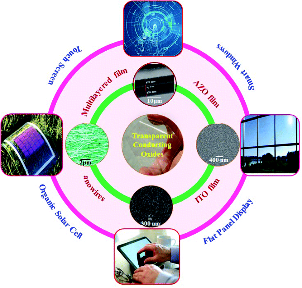 | ||
| Fig. 1 Schematic diagram of various transparent conducting oxides and applications,45–49 presented with permission and copyright. | ||
Tin dioxide as a transparent conducting oxide (TCO) has received huge research attention and been reviewed by several researchers due to its widespread application.9,12,43,44 The review articles have mostly discussed about the challenges and opportunities of ITO. It has both low electrical resistivity and facile patternability12,23 that make it well suited for displays. However, it lacks temperature stability and resistance to chemical attack.10 Although the amount of indium is limited in the earth's crust, the human population is prone to its toxicity.24 The low-rate self-compensation effect makes it more challenging to obtain binary oxide semiconductors having a p-type conductive behavior.27 These challenges provide an impetus to seek an alternative to ITO, which has high electrical conductivity and comparable visible transmittance. To the best of our knowledge, there are no review articles which mainly focus on the metal doped SnO2 for transparent electrodes. Considering the demands of the transparent electrode for opto-electronic devices and renewable energy generation/storage, a more comprehensive review on SnO2 is needed to provide a better representation and guidance of the relevant state-of-the-art research and development.
Furthermore, an advantage of tin dioxide is that it can form oxides of different valences, which provide it with the extraordinary ability to take part in catalysis and charge storage reactions. Tin dioxide (SnO2) is the most stable oxide of tin that finds its use not only as a TCO but also in a number of applications for sustainable development such as sensors, catalysis, energy harvesting and storage due to its earth abundance, non-toxicity and wide band gap. Naturally, a large number of research papers including some good review articles have already been published covering various aspects of tin oxide. For example, Das et al.50 published a comprehensive review of tin oxide, its structure and use as a gas sensor. Jenifer et al.51 reviewed the recent advancements in tin oxide-based thin-film transistors for large-area electronics. Al Hamdi et al.52 reviewed tin dioxide as a photocatalyst for water treatment. The bulk electron mobility of SnO2 is ∼240 cm2 V−1 s−1.53 SnO2 has a wide optical bandgap (3.6–4.0 eV) and a high transmittance over the entire visible regime, which indicates that when it is used in an optoelectronic device its absorption losses can be minimised.53 This wide bandgap is helpful, especially in engineering the energy levels for tandem photovoltaic devices. Other significant advantages of the SnO2 layer include chemical stability and UV-resistance properties which make SnO2 an efficient electron transport layer (ETL), especially in the case of perovskite solar cells. Earlier studies on SnO2 reveal that by alloying with metal oxides or doping with metals, its electronic properties can be selectively tuned to obtain a better optoelectronic device performance.54–56 As many as three reviews have been published within the last three years on the use of tin oxide as the ETL in perovskite solar cells (PSCs),53,57,58 in accordance with the growing interest of researchers on tin oxide as the ETL. The recent development of SnO2 as an anode for dye sensitized solar cells and its impact on the device performance have also been discussed in detail.59–62 The readers are also suggested to consult other relevant references regarding SnO2 as the ETL in organic solar cells, PSCs, and quantum dot LEDs.63–68
Deng et al.69 reviewed the development of SnO2 and graphene nanocomposites as anode materials for lithium ion batteries. However, it is clear that there is not a single review that encompassed the growing applications of SnO2 as the TCO and the ETL in optoelectronic and photovoltaic devices and as an electrode in energy storage devices. In fact, the recent developments on tin dioxide based supercapacitors and Li–sulfur batteries have never been reviewed to date. The review by Deng et al.69 only focused on the tin dioxide–graphene composite as an anode material, but a review of tin oxide based composites (not only with graphene) for anode, cathode and separator is missing.
In view of this, herein, we attempt to review tin dioxide as a material with a different perspective from what has been reviewed already, i.e., a material that has enormous potential for sustainable energy applications focusing on its three major uses as a TCO, ETL and electrode, all of which strongly contribute to circular economies. The review not only tries to sum up and correlate the previous reviews on individual applications of SnO2 but also tries to cover new topics such as the impact of SnO2 for separator modification in Li-ion batteries and for mitigation of the shuttling effect by trapping polysulphides in Li–sulfur batteries. The review is organised as follows. We begin by highlighting the challenges of tin oxide as a TCO and how they are overcome by doping with different metals as well as related computational studies with special focus on earth abundant metals for sustainable applications. Various approaches used by researchers to synthesize SnO2 and doped SnO2 are also reviewed, and the TCO performances of doped tin oxide as a function of dopants such as fluorine (F), antimony (Sb), tantalum (Ta), tungsten (W), molybdenum (Mo), phosphorus (P), and gallium (Ga) are compared. The SnO2/metal/SnO2 structures with respect to TCO performance have been discussed. Next, recent advances in the use of tin oxide as the TCO and ETL in organic light emitting diodes (OLEDs), organic photovoltaics (OPV), perovskite solar cells (including plasma treatment approaches) and building integrated photovoltaic (BIPV) applications are reviewed. This is followed by a comprehensive review of the impact of SnO2, mainly as an electrode material for energy storage devices starting from the most popular Li-ion batteries to Li–sulfur batteries and finally to the rapidly emerging technology of supercapacitors, which have not been reviewed previously. Finally, we summarize the impact of SnO2 on circular economies to conclude this review.
2. Tin oxide as a transparent conductive oxide (TCO)
2.1 Electronic properties of doped SnO2
The electrical and optical properties of TCO materials are determined by their electronic structure. Mishra et al.70 computed an energy–momentum (E–k) diagram for pure stoichiometric SnO2 and Sb-doped SnO2 along several directions in k space indicated by points of high symmetry within the first Brillouin zone. This band structure was computed using the augmented-spherical-wave (ASW) band-structure method for a rutile structure with a unit cell comprising two SnO2 units. The band structure of SnO2 is characterized by a single conduction band that is derived from Sn 5s-orbitals. The Sn-like s character was deduced from the partial density of states function. The conduction band valley is relatively deep with the conduction band minimum (CBM) located at the Γ point. The free electron-like dispersion can be readily seen in the Δ direction (Γ–X) and the Λ direction (Γ–M).70 The pronounced dispersion near the Γ point results in a large curvature for the E–k relation and a small effective mass for conducting electrons. The experimental effective electron mass of conducting electrons in SnO2 is in the range of 0.23–0.3m0 (depending on the direction), where m0 is the electron mass in free space.71 This low effective mass in turn results in a higher electron mobility for conducting electrons in SnO2. By contrast, the valence band which is derived from Sn and O atomic orbitals shows much less dispersion and as a result the holes in SnO2 are generally heavy. The fundamental band gap of 3.7 eV for SnO2 is direct and occurs at the Γ point.Both intrinsic point defects (oxygen vacancies) and extrinsic defects (dopants) introduce localized states in the band structure of SnO2. Kılıç and Zunger showed that oxygen vacancies in non-stoichiometric SnO2 give rise to a shallow defect level at 113 meV below the CBM.72 For Sn interstitials, the corresponding defect level is at 203 meV above the CBM.71 Thus, both these point defects are electrically active and can contribute electrons to the conduction band. The electronic structure of SnO2 can be modified by a high dopant concentration. Mishra et al. computed the theoretical band structure of SnO2 doped by ∼8 at% of Sb (Sn3SbO8) by considering a supercell consisting of two primitive unit cells stacked in the c axis direction with one Sn atom substituted by a Sb atom.70 The cationic dopants form an impurity Sb 5s band within the band gap of SnO2 that has free electron-like dispersion, and this can directly contribute to the conductivity of SnO2. Electrons can also be excited to the next higher band derived from the Sn 5s orbitals. The CBM remains at the Γ point and the band gap is reduced to 2.9 eV. This theoretical calculation shows that Sb and possibly other dopants can alter the band structure of the host SnO2. One important consequence of the strong dispersion near the CBM of SnO2 is that the Burstein–Moss (B–M) effect is readily observed in doped SnO2.73 The B–M effect refers to an increase in the optical band gap in a semiconductor (relative to the fundamental band gap) with increasing dopant density. When the electronic states near the CBM are filled, additional energy is needed to excite electrons from the valence band to the conduction band. The B–M effect is more apparent in semiconductors with low effective electron mass.
In Fig. 2a, a comparison of conduction band alignments that have been reported in the literature is shown. Zr-doping enables up-shifting the energy level with improved band alignment which in turn increases the built in potential.75 For multivalent Sb-doping in a high concentration, the conduction band does not up-shift, but due to the oxidation of Sb, the carrier concentration improved.74 On the other hand, Mg-doping lowers the CBM compared to un-doped SnO2 due to the reduction in free electron density in SnO2.76 The Li-dopant in SnO2 acts as an acceptor and lowers the energy levels of SnO2 as Li+ ions substitute Sn4+.55 In the case of poly(vinylpyrrolidone) (PVP)-doped SnO2, the defect density decreases inside SnO2 and the electron extraction is more effective due to conduction band lowering.77 Y-doped SnO2 can also elevate the conduction band which leads to improved charge carrier transport.78 La and Zn dopants are also very suitable for SnO2 which can uplift the CBM and facilitate the electron extraction and transport with less energy loss.79,80 In the case of Ga-doping into SnO2, the conduction band shifts upward with an increment of electron density and a decrement of deep traps.81 Ta5+ doping inside the SnO2 lattice can increase the oxygen vacancy and thus the conductivity can be increased with free carrier concentration.82
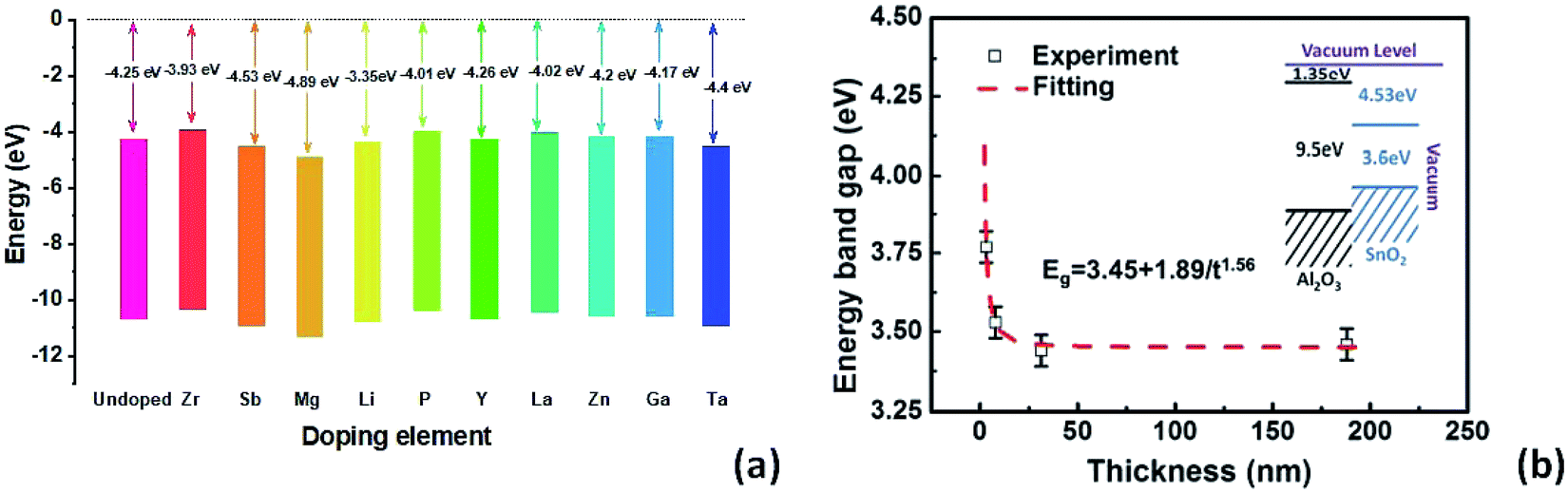 | ||
| Fig. 2 (a) Impact of doping elements on conduction band offsets. (b) Thickness-dependent energy band gap of epitaxially grown Sb doped SnO2 using pulse laser deposition, presented with permission and copyright.74 | ||
It is also worth noting that the oxide thickness plays an important role in energy band gap engineering. Ke et al. demonstrated a thickness induced metal–insulator (MI) transition for epitaxially grown Sb-doped SnO2 on sapphire substrates by pulsed laser deposition.74 A critical thickness is essential for the metallic conductivity in SnO2:Sb thin films (Fig. 2b). The broadening of the energy band gap as well as the enhancement of the impurity activation energy is attributed to the quantum confinement effect.
2.2 Metal-doped tin oxide for improved transparency and conductivity
The key challenges for SnO2 are its high resistivity and bulk defects which can trap carriers and reduce device efficiencies. As a result, selection of a suitable dopant and process design is very important to reduce bulk defects and to increase its electrical conductivity. The conductivity of SnO2 significantly depends on three critical parameters: (1) the dopant, (2) synthesis procedure, and (3) thickness of the oxide layer.83,84 In order to increase the conductivity and achieve a better performance, a different dopant may be required. Visible transmittance, conductivity, and stability of the dopant in SnO2 are very important properties for any alternative to ITO. To the best of our knowledge, a comprehensive review on SnO2 has been published by Das et al.,85 and there are limited reviews that focus on doped SnO2 towards energy harvesting and storage.Aluminium doped ZnO (AZO) and FTO are some of the other commercially available transparent conductive materials. FTO exhibits high chemical resistance, excellent thermal stability, high work function (4.9 eV), strong hardness (6.5 Mohs),86–88 and high optical transparency (T > 80%),89,90 which make it the material of choice as TCOs for different applications. FTO has been used as a window layer in photovoltaic devices, passivation layer for energy-saving smart coatings, transparent conductor for display and flexible devices, electron transport layer, gas sensors, photodetectors, protective coatings, organic light-emitting diodes, and materials for the circular economy.91–97
Even though FTO is a promising candidate for the transparent conductor and electron transport layer, both the conductivity and mobility of FTO are still not comparable with those of ITO. Some of the key challenges affecting the performance and its electrical conductivity of the SnO2 film are the (a) carrier mobility and (b) electron density.22,53,98,99 With the increase of the doping concentration, changes in electronic properties such as the modification of the bandgap, increased carrier concentration and widening of the bandgap by filling low energy levels in the conduction band are observed. As a result of this, the Fermi level shifts up towards the conduction band, causing an increase in the carrier concentration.54,98,100 Several reports have discussed the electrical properties of SnO2, doped SnO2, and SnO2 based multilayer structures.101–111 Li et al. reported nickel-coated FTO (Ni/FTO) through sputtering of Ni layers onto commercially available FTO glass and successive pulsed laser annealing under an external magnetic field (0.4 T) to enhance the electrical performance of FTO.103 Similarly, Chen et al. demonstrated a non-thermal dual-plasma synthesis for antimony doped SnO2, Sb–SnO2 (ATO) nanocrystals with a uniform composition and a conductivity of 0.1 S cm−1 over a high surface area.112 While these methods show an increase in performance, the morphology is affected due to the presence of pinholes after thermal treatment. The lanthanum (La) dopant is a very promising alternative capable of alleviating SnO2 crystal aggregation and it provides a platform with full coverage and helps to form a homogeneous film.80 Furthermore, the La dopant reduces the band offset of the SnO2 layer with increased electron extraction and suppressing charge recombination and thus enhances the power conversion efficiency from 14.24% to 17.08% for perovskite-based solar cells.80
In modern technology, SnO2 based TCOs play a central role in optical and electronic applications. The performance of these devices depends critically on the dopant and the properties of SnO2. Apart from indium (In), doping of tin oxide can be realized with various elements, such as antimony (Sb), fluorine (F), niobium (Nb), tungsten (W), phosphorus (P), strontium (Sr), tantalum (Ta), lanthanum (La), lithium (Li), gallium (Ga), molybdenum (Mo), and cobalt (Co) as these dopants provide precise control over its electrical and optical properties.71,81,101–104,113–130 All these dopants are discussed in this section. For example Sb and F are the most suitable dopants for SnO2,30,101–104,114 wherein Sb substitutes Sn atoms and F substitutes O atoms.89 Sb is an effective dopant because the Sb5+ and Sn4+ ions are of similar radii. In the case of Sb doped tin oxide (ATO), it has high transparency (∼80%) and low resistivity (∼10−3 Ω cm), good mechanical hardness, and environmental stability.88 One key feature of ATO is that its carrier density increases monotonically with Sb doping within the range of 1020 cm−3,86 while the dopant activation efficiency decreases from 60% to 20%. The room temperature Hall mobility of ATO ranges from 6 cm2 V−1 s−1 to 24 cm2 V−1 s−1.
FTO is a stable TCO115,116 that has low electrical resistivity due to the high carrier density.89 It can strongly adhere to any substrate making it suitable for device integration.16 However, its electrical conductivity is not as high as niobium (Nb)-doped tin oxide (NbTO) films.117 Niobium is an exceptional dopant for SnO2 as the ionic radius of Nb5+ (0.064 nm) matches that of Sn4+ (0.069 nm), which enables the substitution of Nb5+ for Sn4+ in the SnO2 crystal lattice structure.118 If SnO2 is concurrently doped with Nb and F to replace the Sn4+ and O2− in the SnO2 lattice, respectively, its Hall mobility and carrier generation will be further enhanced, making it suitable for high efficiency devices.118 The substitution of Nb5+ for Sn4+ and the integration of F− are beneficial in improving the overall performance. The synergistic effect of Nb and F co-doped SnO2 films results in improved optoelectronic properties compared to those of F or Nb-doped SnO2 films.118 Nitrogen is another low-cost and environmentally friendly dopant for SnO2. The nitrogen dopant reduces the optical energy threshold and enhances the film conductivity.115
Recently, molybdenum (Mo) and tungsten (W) doped SnO2 have been studied by Huo et al.119 The Mo-doped and W-doped SnO2 films show an average transmittance of ∼60% over a wavelength range between 300 and 2500 nm, which is ∼2 times higher compared to ITO films.119 Tungsten is an important cation dopant for the SnO2 based transparent conductive material. The electronic and optical properties of SnO2 can be enhanced by replacing Sn4+ through W6+.125 Moreover, W6+ has the highest valence state among the common doping elements to generate more free electrons.125 Doping with W is also very helpful to generate more charge carriers and maintain the structural ability of SnO2.126 Thus, W doped SnO2 might solve the problems related to SnO2 based anode materials for lithium-ion batteries due to its unique characteristics.125 Doping of strontium (Sr) in SnO2 further widens its potential in improving the photocatalytic activity, iteration of the electronic structure, and enhancement of vital physical and chemical properties.127 Studies influencing the third-order nonlinear optical properties of Sr-doped SnO2 were limited, and further elucidation is required for its applications in various optical devices.127 In another study, Bannur et al. observed a third-order nonlinear absorption mechanism for Sr:SnO2 films, which is attributed to free carrier absorption induced two-photon absorption.127 The third-order nonlinear absorption co-efficient (βeff) shows one order of improvement (0.14 × 10⁻¹ cm W−1 to 3.91 × 10⁻¹ cm W−1), which indicates the competency of grown films in nonlinear optical device applications.127
He et al. demonstrated the optical and structural properties of Ta-doped SnO2 monocrystal films grown on MgF2 (110) substrates. The Ta dopant for SnO2 takes the form of Ta5+ ions.128 Ta-doped SnO2 films are of importance due to the high work function of 5.2 eV, with an average transmission over 87%.128 Ta doping for SnO2 films show reduced resistivity and improved Hall mobility.128 The highest Hall mobility of 74.2 cm2 V−1 s−1 is attained for the 5 at% Ta doped SnO2 film, and the least resistivity 2.5 × 10⁻⁴ Ω cm is attained at 6 at% Ta doping.128 It is worth noting that a Ta-doped SnO2 transparent conductive oxide has been demonstrated as a selectively solar transmitting coating for the high temperature concentrating solar power technology.129
Apart from the above-discussed materials, SnO2 can also be doped using aluminium122–124 to achieve p-type conductivity,120 along with annealing at an elevated temperature of 450 °C. In such a process, the electron concentration decreases with aluminum doping due to substitution effects. Gallium (Ga) is another promising p-type dopant for SnO2 since it can substitute Sn atoms with less lattice deformation compared to Al and In.27 The doping of Ga is quite effective in the context of the role of SnO2 in perovskite-based devices. Ga-doped SnO2 is used as an efficient electron transport layer in planar perovskite solar cells (PSCs)81 because of its better band alignment with the perovskite absorption layer for efficient electron extraction.81 Besides, Ga doping reduced the trap state density in SnO2, leading to a lower recombination and negligible hysteresis.81 All these combined to deliver an improved efficiency. Several other dopants in SnO2 that can also improve the PSC performance will be discussed below in the section ‘Impact of SnO2on PSCs’. Cobalt (Co) is also a good substitute for noble metals as the dopant for SnO2. Co ions can easily replace tin ions in SnO2 without destroying the lattice structure because of the compatible ionic radii.130 Also, the Co dopants can enter the tetragonal rutile type SnO2 and suppress the grain growth.130 The doping in SnO2 results in the modification of optical and electronic properties that are needed for various applications.
2.3 Design of doped SnO2 for TCO applications: computational modeling
The computational screening approach for dopants of SnO2 comprises an efficient and reliable calculation of its bandgap, effective mass, binding energy, and the formation energy.12,100,131–133 In recent times, computational screening approaches have shown immense potential in identifying suitable dopants of SnO2 to increase the inherent electrical and optical properties. Towards this end, Cheng et al. investigated the first-principles-based computer screening system in search of suitable dopants or co-dopants for SnO2 to develop new SnO2-based transparent conducting oxide systems.100 Based on computer simulations, it is found that the best candidates for SnO2-based TCO materials are FTO, ATO, phosphorus (P) doped SnO2 PTO (P-doped SnO2) and FPTO (F and P co-doped SnO2).100In another interesting work, Swallow et al. investigated the n-type FTO (n > 1020 cm−3) deposited onto soda-lime glass via atmospheric pressure chemical vapor deposition (APCVD) to reveal inherent self-compensation, which limits the mobility, achievable free electron density, and higher conductivity.22 By using DFT energy calculations, it is determined that the interstitial fluorine in the −1 charge state might be the lowest formation energy acceptor defect for degenerately doped FTO, as shown in Fig. 3a and b.22 Hence, they provided new confirmation of fluorine interstitial as the defect responsible for FTO falling well short of the theoretical ionized impurity scattering with a limited mobility of >100 cm2 V−1 s−1.22
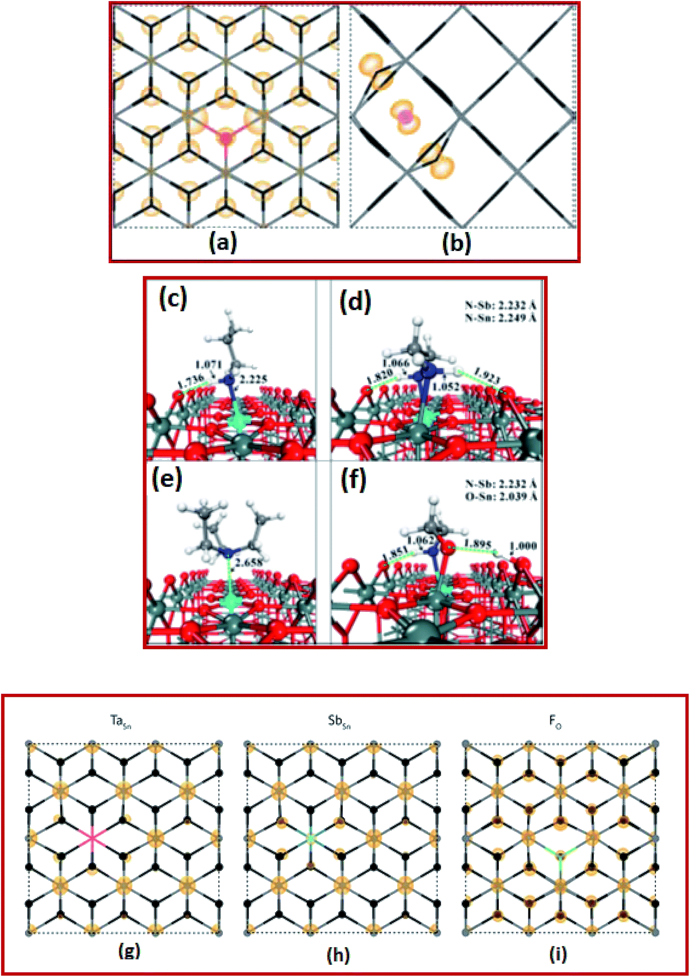 | ||
| Fig. 3 Calculated partial charge densities of (a) FO+ and (b) Fi− in the down and across directions, respectively. The Sn (gray) and O (black) atoms are depicted using a stick model for clarity, while the F atoms are colored red (FO) and pink (Fi) corresponding to the defect color. Charge densities of 0.001 and 0.02 eV Å−1 were used for panels (a) and (b), respectively,22 presented with permission and copyright. The preferred adsorption configurations of (c) propylamine (PA), (d) ethylenediamine (EDA), (e) triethylamine (TEA), and (f) monoethanolamine (MEA) on the ATO (110) surface. The bond distances are given in Å. Color codes: O-red, Sn-gray green, Sb-cyan, C-gray, N-blue, and H-white,106 presented with permission and copyright. The partial charge densities at the CBM of SnO2 for TaSn (g), SbSn (h), and FO (i). The densities highlight the fact that Sb and F both hybridize with the CBM, thus having a detrimental effect on the band curvature with increased doping concentrations, and that Ta does not undergo this same effect,107 presented with permission and copyright. | ||
ATO is more advantageous due to its low cost and abundance. ATO thin films also display excellent electronic and optical properties comparable to those of ITO films and thus ATO is emerging as a promising alternative to ITO. Borgatti et al. elucidated the origin of the satellite structure observed in the Sn 4d core-level photoemission spectrum (PES) of ATO by comparing the experimental measurements to results obtained from ab initio many-body perturbation theory.134 They established that such a satellite structure is produced by the coupling of Sn 4d core electrons to the plasma oscillation of the free electrons observed in the material through doping.134 Moreover, within the same theoretical framework, the enrichment of the asymmetric tail from the valence band photoemission spectrum of doped SnO2 was also explained.134 These results reveal that to capture the satellite structures for narrow-band materials and to identify properly the underlying electronic structure excitations, it is vital to go beyond the homogeneous electron gas (HEG) electron–plasmon coupling model and to perform material-specific ab initio calculations.134 The GW (where G is the one-particle Green's function and W is the screened coulombic interaction) approximation (GWA) for the self-energy and the cumulant (C) expansion of the Green's function were incorporated into the first-principle GW + C scheme to interpret the electron correlation in PES spectra. In this perception, the results for ATO imply that the GW + C theory can be a very promising approach for the interpretation of electron correlation features for PES of several conductive oxide materials.134 Kim et al. investigated the electronic structure of pure and doped SnO2 nanocrystals within a range of 1.3–2.4 nm diameter. Herein, strong quantum confinement effects were observed and the electron binding energy for Sb doped nanocrystals decreases with the size.135
In another study, Chen et al. investigated an instant post-synthesis strategy for aqueous colloidal dispersions of nanocrystals, using ethylenediamine (EDA), propylamine (PA), monoethanolamine (MEA), and triethylamine (TEA).136 By using DFT calculations, they found strong attractive interactions between amines and ATO surfaces via N–Sn and especially N–Sb bonding interactions, as shown in Fig. 3c–f.136 The energies of amine adsorption on the Sb site vary from 0.95 eV to 3.28 eV, following the order of TEA < PA < EDA < MEA, which is at least 0.2 eV higher than the corresponding adsorptions of the Sn site.136 This implies stronger adsorption of amines on Sb sites than on Sn sites. The proposed strategy improved the performance of electrochromic devices such as good reversibility, fast response, and high optical modulation.136 Williamson et al. demonstrated that tantalum (Ta) is a resonant donor in SnO2 using a combination of hybrid DFT calculations, IR reflectivity, and hard X-ray photoelectron spectroscopy.137 It is reported that Ta is a superior dopant to both fluorine and antimony (Fig. 3g–i), with the capacity to yield higher conductivity, mobility, and better IR transparency as compared to FTO and ATO.137 These findings imply that Ta-doped SnO2 has the potential for large surface area applications with low-cost TCO substrates.137
Ganose et al. used DFT to show that incorporation of lead (Pb) into SnO2 reduces the bandgap through lowering of the conduction band minimum, thereby increasing the electron affinity.54 The electron effective mass at the conduction band minimum decreases alongside the bandgap, demonstrating an improved charge carrier mobility.54 Moreover, the calculated optical absorption properties show that the alloys maintain their transparency in the visible spectrum. These properties make SnO2:Pb a more efficient n-type transparent material and an ideal candidate for use in TCO applications.54
Phosphorus (P)-doped SnO2 (SnO2:P), PTO, films were synthesized by an aerosol assisted chemical vapor deposition route with excellent optical and electrical properties.5 A data generator was used to build computational models of P as a dopant for SnO2 and showed that phosphorus acts as a shallow one electron n-type donor allowing improved conductivities. P does not suffer from self-compensation issues associated with other dopants, such as F. This synthetic route opens up the possibility of using a common element to dope SnO2 films for transparent conducting oxide applications.5
3. Design of doped SnO2 for TCO applications: different experimental approaches
As discussed in the previous section, the conductivity of un-doped SnO2 is significantly improved by doping with various dopant elements such as F,103,104 Mn,105,138 Ta,106,107 and Sb.101,102 Tin oxide thin films are usually deposited using solution-based deposition and vacuum-based deposition techniques. Solution-based deposition methods offer numerous benefits over vacuum-based deposition techniques; e.g. simpler processing, better scalability, and lower manufacturing cost.139,140 On the other hand, thin films grown using solution-based techniques have porous surface morphologies, and their electrical properties are relatively poor compared to those of vacuum-based techniques. Several solution-based approaches such as the sol–gel process, hydrothermal synthesis, chemical bath deposition, successive ionic layer adsorption and reaction, and spray deposition are widely reported for doping SnO2 films. To this end, Pasquarelli and co-workers have thoroughly reviewed several solution-based film deposition processes, as elucidated in Fig. 4.139 In this review article, we discuss the doping of SnO2 using solution and vacuum based techniques. Synthesis of high quality doped SnO2 is much sought-after. The impact of dopants on its surface morphology and optical and electronic properties is discussed in detail. | ||
| Fig. 4 Various solution-based approaches for metal oxide film deposition. Reproduced with permission.139 Copyright 2011, The Royal Society of Chemistry. | ||
3.1 Sol–gel and spin coating
Due to its simplicity, sol–gel based processes have gained popularity, and the sol–gel deposition of doped SnO2 films is already well established.141,142 A facile approach has been reported to control the morphology of doped and pure SnO2 films by a sol–gel dip-coating process.143 The root mean square (RMS) roughness value of SnO2:Sb thin films was found to be 1% of film thickness, which makes them suitable for optoelectronic applications. The authors reported a resistivity of ∼10−5 Ωm for the 5 mol% Sb-doped SnO2 films. An average transmittance of >80% (in the UV-vis region) was found for all these films. The bandgap energy of SnO2:Sb varies in the range of 3.69–3.97 eV with an increase in Sb doping concentration.143Shi et al. studied the effect of fluorine concentration on FTO films by the improved sol–gel method.144 The surface morphology, optical properties, and electrical properties of films were investigated for different fluorine concentrations. The grain size increases with an increase in F concentration, as shown in Fig. 5a–f. The particle shape changes from a rod-like structure to a pyramid with an increase of F concentration. This is particularly beneficial for energy conversion devices. The visible transmittance and sheet resistance significantly depend on the F concentration (Fig. 5g and h). The sheet resistance for un-doped SnO2 films is 450 Ω sq−1. However, the sheet resistance decreases from 450 Ω sq−1 to 14.7 Ω sq−1 with the increase of fluorine concentration.144
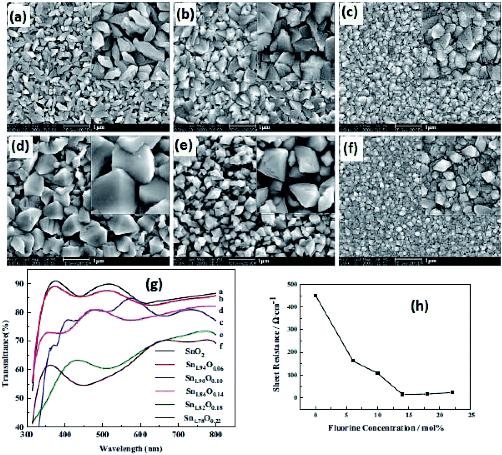 | ||
| Fig. 5 SEM images of films with different F concentrations: (a) SnO2, (b) SnO1.94F0.06, (c) SnO1.9F0.10, (d) SnO1.86F0.14, (e) SnO1.82F0.18, and (f) SnO1.78F0.22. (g) Transmission spectra of films with different F concentrations and (h) sheet resistance of SnO2 films with different F/Sn ratios,144 presented with permission and copyright. | ||
In another study, it is observed that with a lesser number of coatings, the film has larger inter-grain boundaries (i.e. more porous) leading to poor electrical properties. A large number (>7) of sol-layers lead to cracks in the film that decreases the Hall mobility.140 Therefore, an optimum thickness is required to obtain a higher electrical conductivity that, in turn, gives the preferred dense surface morphology for better electrical performance. Jin et al. demonstrated an improved approach in which stannous oxalate (SnC2O4) was dispersed in deionized (DI) water together with citric acid and triethanolamine to obtain a sol–gel solution. The dip-coated film shows a lower sheet resistance of ∼30–40 Ω sq−1.145 Doping of Ta and Nb in SnO2 films by the dip-coating technique achieves moderate electrical properties.146
Gallium (Ga)-doped SnO2 semiconductors show p-type conductivity with an average optical transmittance of more than 87%. Thin film Ga-doped SnO2 was fabricated using a sol–gel spin coating process with a doping concentration of gallium greater than 10%.27 Ga doping reduces the grain size from 7.63 nm to 3.36 nm as the Ga doping concentration increased from 0% to 20%. The RMS surface roughness increased from 2.34 nm at 0% doping to 1.29 nm at 20% and the band gap energy decreased from 3.92 eV for undoped to 3.83 eV for 15% Ga doping. The highest mean hole concentration obtained by this method (1.70 × 1018 cm−3) is slightly lower than that obtained by DC (direct current) magnetron sputtering (8.84 × 1018 cm−3), as reported by Huang et al.147 Moreover, the carrier mobility was found to decrease as the resistivity increased with doping. An organic additive-free aqueous solution based process was reported for the sol–gel synthesis of doped SnO2. Film formation was demonstrated via an evaporation-driven method and dip-coating in a thermostatic oven at 25–60 °C. A crystalline SnO2 film was obtained after heat treatment at 700 °C for 10 min.148 Non-toxic stannous fluoride (SnF2) was also used as a fluorine source to deposit the fluorine-doped SnO2 thin films. The process was referred to as the green sol–gel method. The SnF2 content was varied from 0 to 10 mol% to optimise differing conductivity. The solution was stirred at 80 °C for 2 h and then dip-coated to form FTO thin films, which exhibited a resistivity around 7.0 × 10⁻⁴ Ω cm.149
Film deposition using SnO2 nanoparticles is similar to the sol–gel process and involved pre-synthesized nanoparticles. This process has the advantage that post-deposition annealing at high temperatures is not necessary to achieve crystalline films because nanoparticles are already in the crystalline phase. In another report, Zhao et al. demonstrated a surfactant-free and binder-free deposition of Sb:SnO2 in a compact thin film using Sb:Sn3O4 suspension.150 The as-prepared films have electrical resistivity around 3.04 × 10⁻² Ω cm and a transparency of ∼92.70%.150 Synthesis of highly crystalline Sb–SnO2 nanoparticles is achieved by microwave heating of the antimony acetate and SnCl4 precursors in benzyl alcohol and toluene at 135 °C for 15 min. The spin-coating of ATO dispersion resulted in uniform film deposition with 90% transparency and 1.9 × 10⁻² Ω cm resistivity.151 Deposition of F-doped SnO2 films by Nadarajah et al. involved a reactive tin(II) hydroxide nitrate nanoscale cluster in an aqueous solution. Those films rendered very low electrical resistivity (1.5 × 10⁻⁴ Ω m) and optical transmittance (>85%).152 It is also worth noting that, generally, dopants which formed nanoparticles resulted in a rough surface.
3.2 Chemical bath deposition
A low temperature and single precursor based chemical bath deposition (CBD) approach was presented by Tsukuma et al.153 in which SnF2 was dissolved in DI water, and film growth occurred at 40 °C. After the heat treatment, the electrical properties improved significantly and the resistivity was measured to be ∼1.4 × 10⁻² Ω cm.153 An aqueous solution of SnF2 and HF resulted in a thin film when small amounts of H2O2 and/or H3BO3 were added, but the resistivity was found to be ∼18.7 Ω cm.154 This high resistivity is due to poor crystallinity and the presence of high interface defects for the film synthesized by using CBD and liquid phase deposition (LPD) methods at low temperatures (40–75 °C).154 Raviendra et al.155 demonstrated an electroless deposition of polycrystalline Sb–SnO2 thin films using stannic chloride (SnCl4), ammonium fluoride (NH4F), and silver nitrate in a solution at room temperature. The visible transmittance and reflectance in the infra-red region of pristine SnO2 films were found to be ∼80% and ∼70%, respectively, with resistivity on the order of ∼10−2 Ω cm. In contrast, Sb-doped SnO2 films showed a visible transmittance of 86% and an infra-red reflectance of ∼83% with resistivity in the range of ∼10−3–10−4 Ω cm. The resistivity of the Sb-doped thin films was excellent and comparable to the films deposited using the physical deposition process. When the antimony doping concentration was increased from 0 to 5 at%, the grain size increased from 30 to 65 nm. The larger grain size reduced the grain boundary scattering by reducing the grain boundary potential, which resulted in enhanced mobility and conductivity.155 However, this process required fine control over pH and therefore reproducibility can be challenging.1553.3 Spray coating and aerosol jet
Spray pyrolysis is a widely used deposition technique for achieving high-quality pure and doped SnO2 films on a hot glass substrate (400–600 °C). This process is simple, inexpensive and efficient.87,156,157 It makes the process of adding several dopants easier with a high growth rate and reproducibility and enables mass customization for homogeneous large part deposition.158–160 However, due to high processing temperatures, it can result in certain constraints in depositing the top electrode on functional layers. In these deposition processes, the sheet resistance initially decreases from 189.0 Ω sq−1 to a minimum of 4.1 Ω sq−1 with the increase of the substrate temperature from 250 °C to 300 °C and then saturates.158 In this process, the lattice parameters remain fairly constant with temperature but the crystallinity and transmittance increase, while higher temperatures (>250 °C) result in rougher surfaces. Doping not only affects the preferred orientation but also the source compounds, solvent, and growth parameters (such as the solution concentration, feed rate, and spraying gas pressure). It is claimed that the fluorine doping using the ultrasonic spray technique161 decreases the sheet resistance from about 138 Ω sq−1 to 35 Ω sq−1 and increases the optical bandgap from 3.57 eV for a single crystal SnO2 to 3.77–3.93 eV.Ultrasonic spray pyrolysis of FTO layers on flexible substrates leads to compact grain structures without cracks.162 Muthukumar et al. reported that an increase in the growth temperature from 360 °C to 400 °C results in an average grain size increase from 70 nm to 100 nm and an RMS roughness increase from 6.4 nm to 10.5 nm.162 The Hall mobility increased from 11 cm2 V−1 s−1 to 20.1 cm2 V−1 s−1 and resistivity decreased from 1.3 × 10⁻³ Ω cm to 6.3 × 10⁻⁴ Ω cm, with the increase of growth temperature. With the increase of film thickness from 211 to 480 nm, there was an increase in the average grain size from 85 nm to 110 nm and the RMS roughness from 9.2 nm to 19.2 nm due to competitive grain growth processes.162 Niobium-doped SnO2 thin films of cassiterite tetragonal structure and polyhedron-shaped grains grown by spray pyrolysis are presented.117,163,164 In this deposition process, the optical transmittance increased when compared to that of undoped SnO2, while the absorption edge is red-shifted with an increase in the niobium doping concentration.117
According to Kumar et al., doping with neodymium (Nd) improves the electrical parameters of n-type SnO2 films.165 The resistivity of SnO2 films initially decreased with the Nd doping level up to 4% and further increased for a higher doping level of 6%.165 The change in resistivity was found to be associated with the carrier concentration and grain boundary scattering in the doped SnO2 films. The increment in the carrier concentration and conductivity was related to the increase in Nd dopants that generated more carriers in the SnO2 lattice upon substitution. In a report by Serin et al., the electrical conductivity of spray-deposited polycrystalline un-doped SnO2 films was calculated using a two-point probe method as a function of substrate temperature.166 The Hall mobility and electron concentration as a function of substrate temperature have been studied in detail.166 The highest mobility of 35 ± 1.1 cm2 V−1 s−1 was observed at 300 °C. The mobility decreased with increasing temperature. The conductivity of SnO2 samples was found to be persistent with respect to the substrate temperature. Initially, the electrical conductivity and free-electron concentration increased with the substrate temperature and then fell laterally. However, the Hall mobility first decreased and then increased with increasing substrate temperatures. The Hall mobility values reported for SnO2 films were lower as compared to monocrystalline thin films. The low values of mobility might be due to the hindrance provided by grain boundaries with respect to carrier transport in the SnO2 polycrystalline film. The properties of doped SnO2 films prepared by solution-based techniques are tabulated in Table 1.
| Dopants | Thickness (nm) | Resistivity (Ω cm) | Transmittance (%) | Mobility (cm2 V−1 s−1) | Year | Reference |
|---|---|---|---|---|---|---|
| Undoped | 720 | 1.15 × 10⁻³ | 86 | 0.61 | 2008 | Kasar et al.15 |
| Sb-doped | 525 | 4.7 × 10⁻⁴ | 60 | 11 | 2018 | Ponja et al.3 |
| P-doped | 400 | 7.2 × 10⁻⁴ | 80 | 35 | 2018 | Powell et al.5 |
| Ga-doped | 160 | 0.71 | 87.5 | 8.33 ± 0.16 | 2015 | Tsay et al.27 |
| Nb-doped | 550 | 9.6 × 10⁻⁴ | 71.87 | — | 2013 | Turgut et al.117 |
| Mo-doped | 1.7 × 10⁴ | 1.6 | 60 | — | 2017 | Huo et al.119 |
| W-doped | 1.7 × 10⁴ | 0.61 | 69 | — | 2017 | Huo et al.119 |
| Mo and W co-doped | 1.35 × 10⁴ | 0.35 | 56 | — | 2017 | Huo et al.119 |
| F-doped | 1000 | 4.1 × 10⁻⁴ | 75 | — | 2010 | Miao et al.158 |
| F-doped | 440 | — | 84.61 | — | 2015 | Benhaoua et al.161 |
| F-doped | 211 | 8.9 × 10⁻⁴ | 79.4 | 17.9 | 2013 | Muthukumar et al.162 |
| Sb-doped | 454 | 2.81 × 10⁻³ | 60.55 | 0.347 | 2013 | An et al.140 |
| Sb-doped | 340 | 1.98 × 10⁻⁵ | 72 | — | 2013 | Lekshmy et al.143 |
| Co-doped | 450 | 37.35 | 80 | — | 2010 | Bagheri et al.167 |
| F-doped | 300 | 1 × 10⁻³ | 80 | 28 | 2014 | Wang et al.168 |
The solution-based approach offers a facile and an efficient process to deposit films made up of metal oxide on polyethylene terephthalate (PET) and glass substrates with low cost and scale-up opportunity. Doping of various elements shows the versatility of the solution approach towards the design of highly conducting and transparent tin oxide films. Although there are reports on the film deposition at low temperatures, achieving good crystallinity is critical to obtain desirable electrical and optical properties. Most processes require post-growth heat treatment to achieve high electrical conductivity that again limits their application in low-temperature device fabrication. Therefore, further efforts on the development of nanomaterials based on SnO2 thin films are key to resolve these existing challenges.
3.4 Chemical vapor deposition (CVD) and metal–organic chemical vapor deposition (MOCVD)
Wang et al.168 deposited FTO films by the CVD technique with the inclusion of different additives and reported a carrier mobility of ∼28.5 cm2 V−1 s−1 at a high carrier concentration of ∼4 × 1020 cm−3. The reported high mobility is associated with the development of (200) preferred orientation of the CVD-grown FTO thin films.168 In another work, Ponja et al.3 demonstrated antimony doped SnO2 thin films using aerosol assisted CVD. The samples with 4 at% Sb dopant exhibited an electron mobility of 11.4 cm2 V−1 s−1 and a relatively high carrier density of 1021 cm−3 with a visible transmittance of 60%. Hybrid density functional theory (DFT) calculations reveal the performance limit beyond a certain dopant level and the appearance of Sb(III) within the doped thin films.3 Phosphorus doped SnO2 which displays excellent electrical properties and optical properties was synthesized by using aerosol assisted CVD (AACVD).5 Phosphorus concentration plays a key role in obtaining high mobility and high visible transmittance. Both the surface morphology and crystallinity depend on the phosphorus concentration.5Ta-doped SnO2 films were deposited on α-Al2O3 (012) substrates by using a MOCVD method. The deposited films showed an average transmittance of >88% in the visible wavelength range.169 When the Ta concentration was increased from 0 to 8 at%, the transparency range extended to the UV-B spectral region (i.e. 280–320 nm), and the optical bandgap of the films increased from 3.96 to 4.30 eV.169 Furthermore, 4 at% of Ta doped SnO2 films showed the highest Hall mobility of 58.1 cm2 V−1 s−1, and the lowest resistivity of 4.0 × 10⁻⁴ Ω cm was obtained at 6 at% of Ta doping concentration.169 Ta-doped SnO2 epitaxial films demonstrate beneficial electrical properties and transparency extending to the UV-B light region, indicating a wide range of applications from transparent electric to photoelectric devices.169
3.5 Doping of SnO2 through physical vapor deposition methods
Thin-film SnO2 can be synthesized by using different physical vapor deposition techniques, namely, magnetron sputtering, pulse laser deposition, thermal evaporation, and electron beam evaporation. Fig. 6 depicts the different techniques employed to synthesize SnO2 thin films. Physical vapor deposition techniques provide high-quality thin films when compared to solution-based methods. The film thickness, composition, and electronic properties can be tuned precisely. The sputter deposition technique is commonly used for SnO2 deposition. It is a widely accepted and used technique for numerous applications including metal electrodes, transparent conductors, gas sensors, liquid crystal displays, LEDs, thin-film solar cells, and dielectric layers in low emissivity coatings for energy-saving smart windows. Due to its higher deposition rate, excellent reproducibility, competitive cost, and the possibility of using commercially available large-area sputtering systems, magnetron sputtering is a preferred technique.2,26,31,170–175 Numerous reports have been made to grow SnO2 thin films by doping using the direct sputtering technique.89,115,172–179 DC magnetron sputtering offers a high deposition rate, uniformity over a large-area substrate and provides easy control over the composition of films. SnO2 films with single phase tetragonal polycrystalline structures can be deposited by sputtering and annealing in air at different temperatures. It is also worth noting that the crystallization of films grown at high substrate temperatures is enhanced.178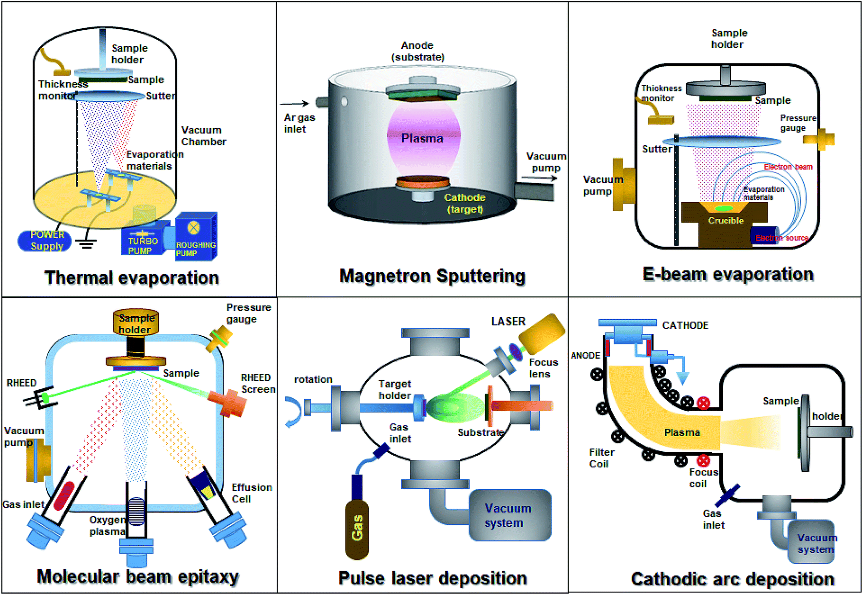 | ||
| Fig. 6 Vacuum based physical vapor deposition techniques. | ||
Banyamin et al.89 demonstrated the electrical and optical properties of FTO deposited by mid-frequency pulsed DC magnetron sputtering89 from a loosely packed blended SnO2 and F2 powder to produce homogeneous n-type thin films at low temperatures without post-deposition treatment. This method has several advantages: (1) enhanced sputtering rate without any need for reactive process control equipment, (2) low deposition temperatures, (3) suppression of arcs, and (4) the formation of dense homogeneous films. Furthermore, the loosely packed powder avoids target cracking and allows variation of the composition.89 Apart from the scattering losses at surfaces, sputter-deposited FTO has high transparency (82–85%) in the visible region, which is independent of doping. In this process, the mean crystallite size increases with both the fluorine content and temperature, but diminishes with excess fluorine due to the solubility limit. The bandgap increases slightly with F doping (from 3.70 to 3.77 eV).
Polycrystalline tantalum-doped tin oxide (TTO) films can be deposited onto amorphous substrates to obtain lower resistivity using the radiofrequency (RF)-magnetron sputtering method.177 Thin film resistivity in such processes decreases exponentially from 1 to 1.7 × 10⁻³ Ω cm with respect to the substrate temperature. These resulted in an average optical transmittance decrease from 97% at 600 °C to 91% at 700 °C. The charge carrier density increased from 3.6 × 1018 cm−3 at 300 °C to 3.3 × 1020 cm−3 at 700 °C, while the Hall mobility increased from 1 to 12 cm2 V−1 s−1. With an increase in the oxygen ratio in the process gas mixture, the charge carrier density initially dropped and then increased, thereby decreasing its mobility, transmittance, and grain size. It is possible to prepare nitrogen-doped tin oxide in an amorphous phase onto flexible PET substrates by RF magnetron sputtering.115 Increasing the oxygen partial pressure produces oxygen-rich smoother and more uniform films, thereby increasing the transmittance (about 80% in the visible region) and the optical band gap (from 3.19 to 3.42 eV for 1 to 4% partial pressure). The resistivity of nitrogen-doped SnO2 is in the range of 9.1 × 10⁻⁴ Ω cm.
Low-temperature reactive DC magnetron sputtering can also be used to prepare antimony doped tin oxide films on glass and graphite substrates using a metallic tin target, without additional heat treatment.179 The electrical resistivity of such films varies with the oxygen content in the sputtering gas atmosphere as it influences the optical properties such as changes in color (yellow at 10% but brown at 16% oxygen). It also provides moderate transmission whereby at 17% oxygen, the average optical transmittance is about 74%. Besides, the bandgap energy increases with the oxygen content from 2.2 eV at below 17% to approximately 3.6 eV at 17% of SnO2.
Dopant elements, the synthesis mechanism and postdeposition treatments play an important role in achieving high electrical conductivity and optical transparency for TCOs.180,181 The Sb-, Ta-, Nb-, F-, arsenic (As)-, and tungsten (W)-doped SnO2 thin films have been widely explored.86,182,183 Even though Sb is the frequently used dopant for SnO2 films for optoelectronic device applications,86,172 the persistent issue is the strong resistivity dependency on the film thickness.171 In general, when the thickness is decreased by tens of nanometers, the resistivity of TCO thin films increased significantly.171 Shihui Yu et al. developed Sb-doped SnO2 (ATO) thin films with varying thicknesses on a glass substrate by magnetron sputtering and proposed a mechanism of varying electrical properties with respect to film thickness.171 In 2019, Bhasker Parida et al. deposited high-quality ITO films by RF magnetron sputtering with post-thermal annealing in a nitrogen environment.184 The high quality of ITO films is attributed to the combined effects of effective suppression of oxygen incorporation into films due to the post-annealing process.184
Liao et al. and Kim et al. also reported the conductive properties of SnO2 films by introducing H2 into sputtering plasma.185,186 Thin films of FTO were prepared by pulsed DC magnetron sputtering with a metal tin target through two different modes: the transition mode and the oxide mode. In the transition mode, the CF4 gas flow rate was varied, whereas, in the oxide mode, the CF4 gas flow was fixed, but the H2 gas flow was varied.185 A minimum resistivity of 1.63 × 10⁻³ Ω cm with an average visible transmittance of 80.0% was obtained for the transition mode, whereas in the oxide mode the resistivity reduced to 8.42 × 10⁻⁴ Ω cm with an average transmittance of 81.1%. Kim et al. investigated the effect of using hydrogen plasma treatment on the structural and electronic properties of sputter-grown SnO2.186 The electrical conductivity of the film increases due to the generation of oxygen vacancies after hydrogen plasma treatment. On the other hand, hydrogen plasma treatment etched SnO2 films and subsequently degraded their crystalline quality and optical transmittance. Zhu et al. prepared FTO films by using RF magnetron sputtering with a SnO2–SnF2 target in an Ar + H2 atmosphere. The introduction of H2 during sputtering can improve the conductivity of FTO films. It was also revealed that the base pressure has a notable influence on the structural properties of FTO films.187 The performance of TCO is considerably affected by the crystallinity and surface morphology of the film.188,189 Smoother surfaces reduce the contact resistance and localized field effects,190,191 whereas rougher or patterned surfaces affect the amount of light absorbed by the active layers due to entrapment of incident light (by scattering the incoming light and increasing the optical path length of light within the solar cells).192,193 A pyramidal surface is found to have a larger transmission and efficiency than those of a rectangular surface.188 The surface morphology and grain orientation of a film are affected by its own thickness.194 The electrical conductivity and transmittance of the film increases and decreases, respectively, with increasing thickness of the film.156
Engineering the morphology is important for specific applications, and roughness in relation to morphology can be tuned by incorporating additives during the process.195 It is also worth noting that the resistivity depends on the crystalline orientation.10 Investigation of doped SnO2 by trivalent ions using the pulsed layer deposition (PLD) technique reveals that the films exhibit preferential orientation and have an average transmittance of 83–86%. The resistivity decreases with the increase of doping from 0% to 6%; however, for doping with >6%, the resistivity increases.196 Fukumoto et al. demonstrated epitaxially grown high mobility Ta-doped SnO2 films on TiO2 substrates using pulsed laser deposition.197 Ta-doped SnO2 (Sn1−xTaxO2, TTO) thin films epitaxially grown on TiO2 (001) substrates using pulse laser deposition showed a very high Hall mobility of 130 cm2 V−1 s−1 at room temperature with a carrier density of ∼1020 cm−3 (Fig. 7). It is also worth noting that the Ta5+ ions are substituted for the Sn4+ sites and generate one electron per Ta, which suggests 100% doping efficiency for the Ta dopant. The properties of doped SnO2 films prepared by vacuum-based techniques are summarized in Table 2.
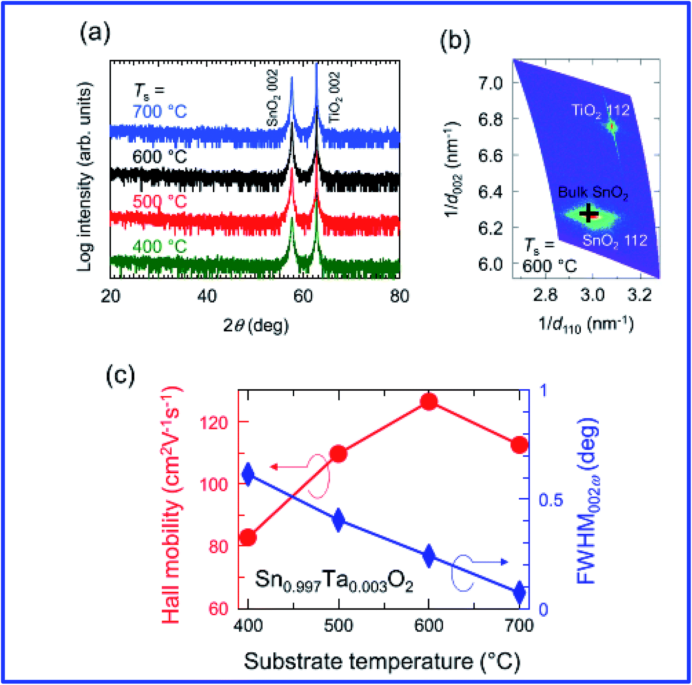 | ||
| Fig. 7 (a) ω–2θ X-ray diffraction patterns for Sn1−xTaxO2 (TTO) films with x = 3 × 10⁻³ grown at various substrate temperatures (Ts). (b) A reciprocal space map around the asymmetric 112 diffraction peaks for a TTO film grown at Ts = 600 °C. A cross represents the peak position for bulk SnO2. (c) Ts dependence of Hall mobility (μH, circles) and full width at half maximum of the rocking curve (ω scan) for the 002 diffraction peak (FWHM002ω, diamonds) for the TTO (x = 3 × 10⁻³) films, where Ta5+ ions were substituted for the Sn4+ sites and generated one electron per Ta (100% doping efficiency),197 presented with permission and copyright. | ||
| SnO2 | Thickness (nm) | Resistivity (Ω cm) | Transmittance (%) | Mobility (cm2 V−1 s−1) | Year | Reference |
|---|---|---|---|---|---|---|
| F-doped | 400 | 6.71 × 10⁻³ | 83 | 15.1 | 2014 | Banyamin et al.89 |
| AlN-doped | 200 | 0.05 | 90 | 5 | 2015 | Wu et al.120 |
| Al-doped | 1050 | 0.81 | 80 | 1.1 | 2010 | Entradas et al.121 |
| Al-multilayer | SnO2: 200 | 1.38 | 80–81 | 0.399 | 2014 | Park et al.175 |
| Al: 25 | ||||||
| N-doped | 100 | 9.1 × 10⁻⁴ | 80 | — | 2015 | Fang et al.115 |
| N-doped | 8 × 10⁻² | Above 80% | 6.75 | 2019 | Nguyen et al.198 | |
| Sb-doped | 220 | 1.8 × 10⁻³ | 11.6 | 2015 | Bissig et al.86 | |
| Sb-doped | 300 | 4.9 × 10⁻³ | 74 | — | 2010 | Boltz et al.179 |
| Sb-doped | 700 | 3 × 10⁻³ | 80 | 6.5 | 2010 | Montero et al.199 |
| Cu-multilayer | SnO2: 0 | 0.29 | 87 | — | 2014 | Yu et al.200 |
| Cu: 14 | 7.79 × 10⁻⁵ | 54 | — | |||
| Zn-doped | 850–900 | 7.436 | 80 | 35.14 | 2012 | Ni et al.201 |
| Ta-doped | 1.7 × 10⁻³ | 91 | 12 | 2014 | Weidner et al.177 | |
| Ta-doped | 400 | 5.4 × 10⁻⁴ | 85 | 25.7 | 2016 | Weidner et al.202 |
| Ta-doped | ∼120 | 6.0 × 10⁻⁴ | — | 130 | 2020 | Fukumoto et al.197 |
| Ta-doped | 453 | 4 × 10⁻⁴ | 88 | 58.1 | 2019 | He et al.169 |
| Cd-doped | 82 | 1.78 × 10⁻³ | 84 | — | 2012 | Flores et al.203 |
The synthesis mechanism plays an important role in SnO2 based TCOs. The surface morphology, chemical composition and bulk defects depend on the synthesis process.204 In general, the vacuum based technology provides better uniformity of the film and lower bulk defects over solution based techniques. Chemical composition can be precisely controlled using a vacuum based process. However, the solution based process provides easy synthesis, nanostructure tuning, and large scale production. Table 3 describes the advantages and challenges for different synthesis processes for SnO2.
| Methods | Advantages | Disadvantages | Applications |
|---|---|---|---|
| (1) Sol–gel process | (i) Low-cost and simple technique | (i) Synthesis of ultra-thin films (<10 nm) | (i) Optoelectronic devices |
| (ii) Reproducibility | (ii) Low wear-resistance, porosity and crystallinity | (ii) Thin films and coatings | |
| (iii) Achieves proper stoichiometry | (iii) Large scale production | (iii) Microelectronic devices | |
| (iv) Low-temperature sintering process | (iv) Easy cracking during the drying stage | (iv) Nanostructure synthesis | |
| (v) Functionalization | (v) Presence of bulk and interface defects | (v) Catalysis for renewable energy | |
| (vi) Renewable energy and energy storage devices | |||
| (2) Chemical bath deposition | (i) Low temperature process | (i) Long-period deposition | (i) Thin films and coatings |
| (ii) Single/multiple precursor | (ii) Synthesis of ultra-thin films (<10 nm) | (ii) CdS layer for CIGS and CZTS based solar cells | |
| (iii) Easy synthesis | (iii) Presence of bulk and interface defects | (iii) Transparent conductors and devices | |
| (iv) Tunability of film structure and grain size | (iv) Various doping design and synthesis | (iv) Micro-electronic devices | |
| (v) Achieves proper stoichiometry | (v) Seed layer requirement | (v) Thin film based catalysis for renewable energy | |
| (vi) Strong adhesive | (vi) Optical coatings | ||
| (vii) Large scale production | |||
| (3) Spray coating | (i) Simple, inexpensive and efficient | (i) Requires high temperature | (i) Functional coatings |
| (ii) Several dopants with a high growth rate and reproducibility | (ii) Lower conductivity | (ii) Energy conversion and storage | |
| (iii) Mass customizations | (iii) Energy consumption | (iii) Solar cells | |
| (iv) Excellent compositional homogeneity | (iv) Wastage of solution | (iv) Highly active catalysis | |
| (v) Large-area coating | (vi) Synthesis of ultra-thin film | (v) Supercapacitors | |
| (vi) Hydrophobic and hydrophilic coatings | |||
| (vii) Opto-electronic devices | |||
| (4) Spin coating | (i) Easy synthesis | (i) Lack of material efficiency | (i) Microelectronic semiconductor industry |
| (ii) Can achieve a suitable thickness of the film | (ii) Scalability | (ii) Optical lenses | |
| (iii) Excellent for laboratory scale | (iii) Wastage of material | (iii) Photoresist-coating | |
| (iv) Quick deposition | (v) Stoichiometry | ||
| (v) Easy integration | (vi) Dopant incorporation | ||
| (5) Chemical vapor deposition | (i) Ultra-thin film | (i) Expensive and complex process | (i) Microelectronic semiconductor industry |
| (ii) High crystal quality | (ii) Scalability | (ii) Wafer growth | |
| (iii) Stoichiometry | (iii) Wide range of doping selection | (iii) High quality dielectric/insulator | |
| (iv) Epitaxial growth | |||
| (6) Hydro/solvo thermal | (i) Simple technique | (i) Long-time reaction | (i) Large scale synthesis |
| (ii) Low cost | (ii) Safety issues | (ii) Biomedical | |
| (iii) Large scale synthesis | (iii) Crystal quality | (iii) Gas sensors | |
| (iv) Ultra-thin film | (iv) Thin/thick film | ||
| (7) Atomic layer deposition | (i) High-quality film | (i) Time processing | (i) Nano-coatings |
| (ii) Low-temperature processing | (ii) Economic viability | (ii) Transparent conductor | |
| (iii) Stoichiometric control | (iii) Limitation of materials | (iii) Nanodevices | |
| (iv) Excellent adhesion | (iv) Large area deposition | (iv) Catalysis and environment | |
| (v) Ultra-thin films | (v) Energy conversion/storage | ||
| (8) Thermal evaporation | (i) Synthesis of thin films over a large area with uniform thickness | (i) Lower environmental stability | (i) Optical coating |
| (ii) Low cost and reproducible film quality | (ii) Mechanical durability | (ii) Light-emitting diode and photovoltaic devices | |
| (iii) High temperature processing | (iii) Electrodes for semiconductor devices | ||
| (iv) Dielectric based multilayer for energy harvesting and saving | |||
| (9) Sputtering | (i) High-quality film | (i) High cost | (i) Optical coatings |
| (ii) Ultra-thin layer | (ii) High power deposition damage surface | (ii) Smart coatings | |
| (iii) Scalability | (iii) Composition | (iii) Nanodevice fabrications | |
| (iv) In situ doping using stoichiometry | (iv) Transparent conductor | ||
| (v) Low temperature processing | (v) Energy saving coating | ||
| (vi) Photovoltaic devices | |||
| (vii) Metal electrode |
4. Multilayered SnO2/metal structures for improved TCO performance
4.1 SnO2/metal/SnO2 multilayers
Multilayers of SnO2 were studied for different applications, such as the transparent conductor, low emission glass, transparent heater, etc. They typically consist of oxide-metal-oxide (OMO) trilayers. The oxide layers in such materials are composed of different oxides such as TiO2, ZnO, SnO2, and ZrO2. Such arrangements are quite beneficial as they provide high transmittance and higher conductivity due to the presence of a metal layer. SnO2/metal/SnO2 multilayer structures show promising characteristics for the transparent conductor and smart coating applications.2 SnO2–Cu–SnO2 based multilayers are deposited onto quartz substrates using DC/RF magnetron sputtering.200 Metal-based multilayer structures have low resistivity (ranging from about 0.29 Ω cm for pristine to 7.79 × 10⁻⁵ Ω cm for the 14 nm thin copper film), with comparable optical transmittance in the visible spectrum (∼73% for 4 nm copper thickness, which decreases to 54% with an increase of the copper layer thickness to 14 nm, as shown in Fig. 8a and b). Apart from that, the multilayer films were thinner and more durable than single-layered TCO and single-layered metal films, respectively. The optical bandgap energies decrease from 4.27 eV to 3.77 eV for 14 nm Cu thickness (Fig. 8c). With the increase of the substrate temperature from 100 °C to 300 °C, the resistivity decreases and reaches its minimum value of 6.5 × 10⁻⁵ Ω cm (Fig. 8d). A further increase in the substrate temperature leads to a drastic increase in the resistivity.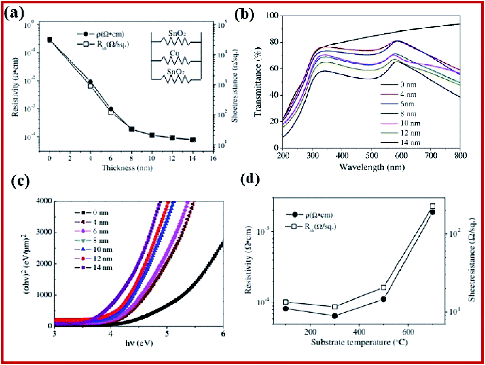 | ||
| Fig. 8 (a) Resistivity and sheet resistance of SnO2/Cu/SnO2 multilayer films deposited at 500 °C as a function of Cu layer thickness. (b) Optical transmittance of SnO2/Cu/SnO2 multilayer films deposited at 500 °C. (c) The (αhν)2 relation for SnO2/Cu/SnO2 multilayer films. (d) Sheet resistance and resistivity of SnO2/Cu/SnO2 multilayer films developed at different substrate temperatures,200 presented with permission and copyright. | ||
Sandwich structured Zn/SnO2/Zn multilayer thin films can also be prepared on quartz glass substrates using DC and RF magnetron sputtering processes, followed by thermal treatment to obtain p-type thin films.201 SnO2:Zn thin films exhibiting p-type behavior with a resistivity of 7.436 Ω cm and a carrier concentration of 2.389 × 1017 cm−3 with transparency exceeding 80% were obtained at optimum annealing (400 °C for 6 hours). Besides these, n-type films were also obtained for the sample annealed at 300 °C for 6 hours, which might be attributed to the inability of Zn atoms to substitute Sn at lower temperatures due to the lack of activation energy. Multilayer p-type SnO2/Al/SnO2 thin films were prepared on a quartz substrate by using RF sputtering techniques and consequent annealing, which increased the resistivity (from 1.38 Ω cm at 1 h to 6.42 × 10⁵ Ω cm at 8 h) and the average transmittance (∼80–81%).175
The SnO2/Ag–Pd–Cu (APC)/SnO2 multilayer films for high performance flexible and transparent thin-film heaters were investigated by Kim et al.205 The SnO2/Ag–Pd–Cu (APC)/SnO2 multilayer films were prepared using a multi-source evaporation method.205 In this method, the sheet resistance of 9.42 Ω sq−1 and the optical transmittance of 91.14% were observed for the as-grown multilayer structure.205 In the case of multilayer formation, Mn–SnO2 (MTO)/Ag/MTO thin films were prepared on a flexible polyethylene terephthalate (PET) substrate using a DC/RF sputtering system.206 The transmittance of MTO/Ag/MTO multilayer films with a 550 nm thickness increased from 83.1% to 87.9% with an increase in the sheet resistance from 6.3 to 9.8 Ω sq−1 upon increasing the O2/(Ar + O2) flow rate.206 The highest figure of merit of the MTO/Ag/MTO multilayer film was 45.7 × 10⁻³ Ω−1 at an O2/(Ar + O2) flow rate of 2.8%.206 These results indicate that the MTO/Ag/MTO multilayer thin films deposited on PET substrates have high transmittance and low resistance, which make them promising materials for future flexible devices.206
On the other hand, Hwang et al. developed a three-layered TiO2/BiVO4/SnO2 (T/B/S) photo-anode which demonstrated enhanced photo-electrochemical (PEC) water oxidation performance at high visible transmittance above 510 nm wavelengths.208 The T/B/S photo-anode deposited by the solution spin coating method consists of three layers of sequential deposition.208 The underlying SnO2 layer creates an increased lateral grain size (∼600 nm) of the BiVO4 layer and formed a type-II heterojunction for efficient improvement in charge separation and electron transport properties.208 The T/B/S photo-anode exhibits higher photocurrent density at 1.23 V versus reversible hydrogen electrode (∼2.3 mA cm−2 for water oxidation and ∼3.7 mA cm−2 for H2O2 oxidation). Also, it exhibits higher stability in comparison to BiVO4/SnO2 and pristine BiVO4 photo-anodes.208 The SnO2 based multilayer is a prospective technology for solar cells, solar hydrogen generation, smart coating, and flexible device applications.167,207,209 The performance of the multilayer depends on the metal layer and oxide layer. Zinc tin oxide (ZTO) shows promising characteristics for transparent conductor applications, owing to its low sheet resistance, low cost, and high transmittance. This particular set of film consists of ZTO–M–ZTO layers in which the metal M in the multilayer structure is Ag. The multilayers were deposited using RF and DC magnetron sputtering (Fig. 9a and b). The electrical properties of these multilayers were studied as a function of Ar gas flow. By decreasing the Ar gas flow from 180 to 30 sccm, the resistivity of ZTO film decreased from 0.22 to 0.09 Ω cm. However, the resistivity increased with an increase in the O2/Ar + O2 gas flow. In such multilayers, the thickness of interlayers influences the sheet resistance. For example, the sheet resistance of ZTO film depends on the thickness of the Ag layer. The SEM images (Fig. 9c) show the morphology and thickness dependence of the Ag layer and its influence on the sheet resistance of the film. In another study, the optical transmittance and the sheet resistance of multilayer structures of various metal-doped SnO2 are shown in Fig. 9d. The resistivity of FTO is shown in Fig. 9e. As the fluorine content increases, the resistivity increases. The electrical resistivity of the FZTO film is reported to be 8 × 10⁻⁵ Ω cm.207 These SnO2 based multilayers are widely used as electrode materials in organic photovoltaic (OPV) applications.
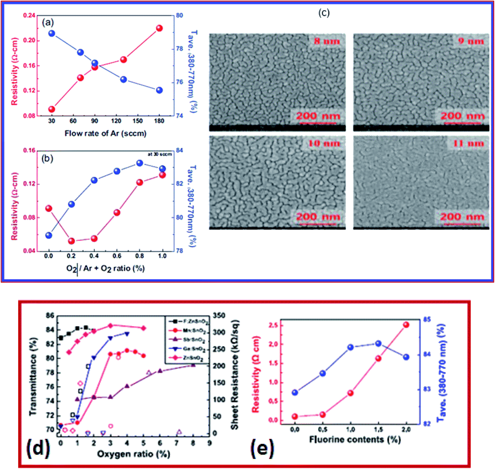 | ||
| Fig. 9 (a) Resistivity of ZTO films at different argon flow rates. (b) The O2/Ar + O2 ratio is 30 sccm. (c) Surface morphology of the silver layer on ZTO/glass with increasing thickness,108 presented with permission and copyright. (d) Average transmittance and sheet resistance of different doped tin oxide (SnO2) thin films. (e) Resistivity and average transmittance versus fluorine content,207 presented with permission and copyright: Conductive and transparent, structured tri-layer deposited on a substrate. | ||
The surface morphology of metal oxides plays a crucial role in the growth of a uniform metal layer for the OMO multilayer. The performance of the OMO based TCO depends on both the metal layer and the oxide layer. The surface morphology depends on the thickness of the oxide layer (Fig. 10a–j).210 Thus, it is essential to optimise the thickness of the metal oxide (e.g. SnO2 or ZnO) to grow a continuous ultra-thin metal layer over the SnO2 layer. It is worth noting that the critical thickness for continuous growth of the metal layer also depends on the surface roughness of the dielectric layer (Fig. 10k and l).210 Growth of an ultra-thin metal with a smooth surface is crucial to enhance the performance of the TCO using an OMO structure. The impact of the seeding layer on the growth of high quality thin metals can also be found in ref. 2 and 210. It is worth noting that the OMO multilayer suffers metal and oxygen diffusion during thermal treatment. Thus, the performance of the OMO based structures requires interface engineering to reduce the metal (Ag) and oxygen diffusion into adjacent layers during high-temperature annealing. Recently, Hwang et al. demonstrated sputter-grown thermally stable SnO2/Ag/SnO2 transparent electrodes using Ni-doped Ag with improved performance due to the reduction of defects.211Table 4 summarises the impact of a multilayer based transparent conductor on the device performances.
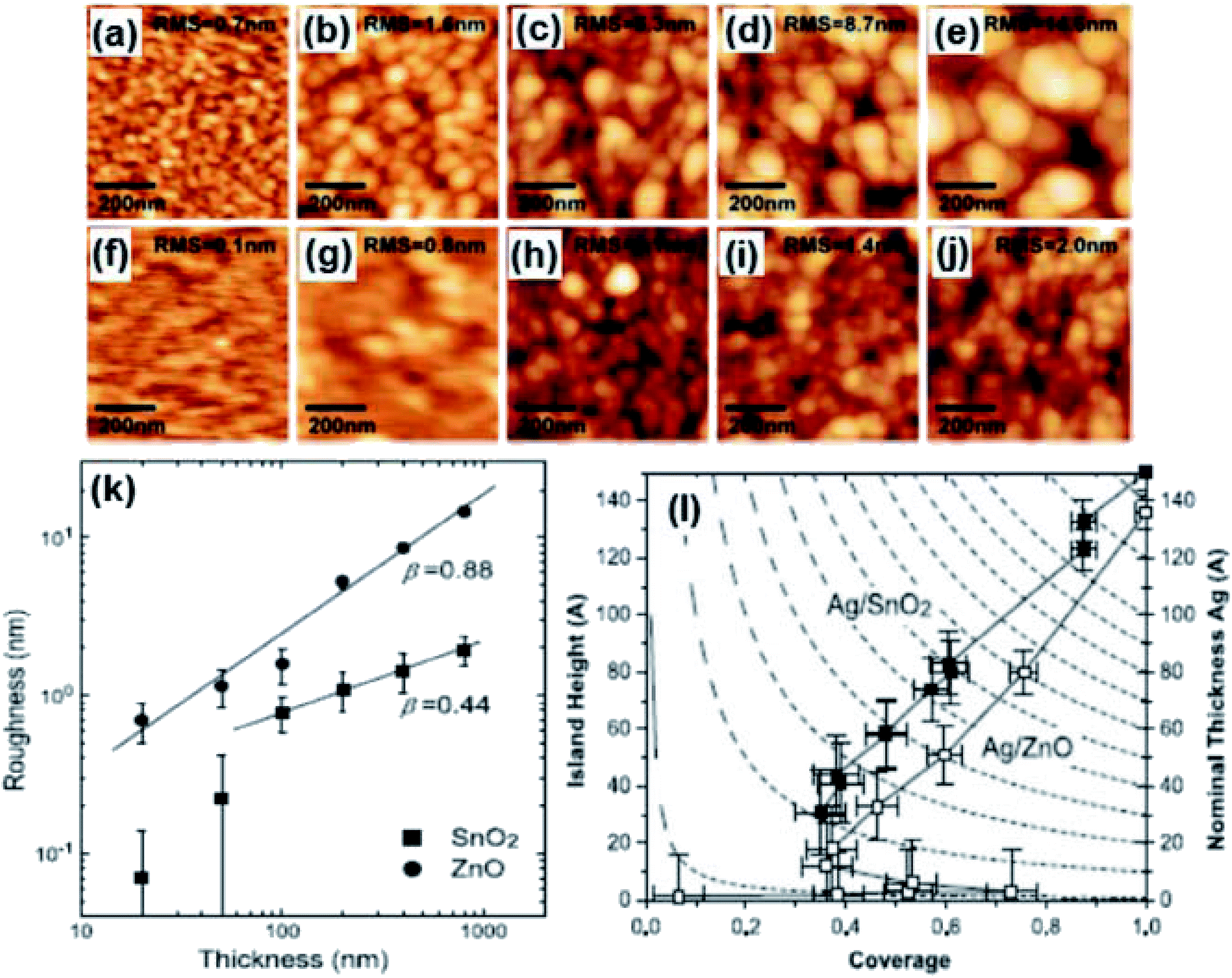 | ||
| Fig. 10 AFM images of the surface of ZnO and SnO2 thin films of increasing thickness. ZnO: (a) 20 nm; (b) 100 nm; (c) 200 nm; (d) 400 nm; and (e) 800 nm. SnO2: (f) 20 nm; (g) 100 nm; (h) 200 nm; (i) 400 nm; and (j) 800 nm. (k) Representation of the roughness versus the thin film thickness for ZnO and SnO2 thin films. (l) Representation of the island height against the surface coverage for successive evaporation of silver on the surface of ZnO and SnO2 thin films. The dotted lines represent the theoretical curves corresponding to equivalent amounts of silver.210 Reprinted from ref. 210, Copyright 2013, with permission from Elsevier. | ||
| SnO2/metal based multilayer | Resistivity | Sheet resistance | Optical transmittance | Thickness | Reference |
|---|---|---|---|---|---|
| SnO2–Cu–SnO2 | 7.79 × 10⁻⁵ Ω cm | — | 54% | 14 nm | Yu et al.200 |
| Zn/SnO2/Zn | 7.436 Ω cm | — | 80% | — | Ni et al.201 |
| SnO2/Al/SnO2 | 6.42 × 10⁵ Ω cm | — | 80–81% | — | Park et al.175 |
| SnO2/Ag–Pd–Cu (APC)/SnO2 | — | 9.42 Ω sq−1 | 91.14% | — | Kim et al.205 |
| Mn–SnO2 (MTO)/Ag/Mn–SnO2 (MTO) | — | 9.8 Ω sq−1 | 87.9% | 550 nm | Kim et al.206 |
| SnOx–Ag–SnOx | 5.6 × 10⁻⁴ Ω cm | 9.8 Ω sq−1 | — | — | Bou et al.212 |
| Mn-doped SnO2 (MTO)/Ag/MTO | 10.1 Ω sq−1 | — | — | 40 nm | Lee et al.209 |
| FTO/Ag/FTO | 8.8 × 10⁻⁵ Ω cm | — | 95.5% | 7 nm | Yu et al.11 |
4.2 Grid-structuring of the SnO2/metal/SnO2 multilayer
Grid structuring is another promising technique that has been studied for OMO multilayer materials.212 The lift-off process is used without affecting the electrical properties of the materials. Bou et al. investigated the grid structuring of the SnOx–Ag–SnOx multilayer.212 These multilayers are deposited using an e-beam evaporator. The grid structures provide low resistivity and high transmittance and are used as an anode in organic photovoltaic (OPV) devices. The surface coverage of such structures affects the properties of the multilayer thin film. The electrical measurements for the aforementioned grid tri-layered structure were carried out using an in-line four-probe method. The sheet resistance for the as-grown multilayer structure is measured to be 9.8 Ω sq−1. The resistivity of grid-based multilayers varies with the surface coverage. The resistivity increases with decreased coverage from a value of 2.9 × 10⁻⁴ Ω cm for the full tri-layer to 5.6 × 10⁻⁴ Ω cm for the most transparent multilayer.212The Mn-doped SnO2 (MTO) multilayer structure is proven to be an efficient system (Fig. 11).209 The MTO/Ag/MTO multilayer electrode was deposited onto a patterned glass substrate by RF sputtering at room temperature. The electrical resistivity in a binary layered structure Ag/MTO/glass depends on the thickness of Ag.108,209 As the thickness of Ag is increased, the resistivity decreases. This decrease in resistivity may be attributed to the increase in the carrier concentration and hence the mobility (Fig. 11a). According to this study, the sheet resistance of the MTO/Ag/MTO layered structure was reported to be 10.1 Ω sq−1 for the 40 nm thick MTO film. This result is similar to that of commercial ITO. Due to these properties, MTO based heterostructures were applied as electrode materials for solar cells. The current density of the MTO/Ag/MTO multilayer electrode is compared with the commercial ITO, as shown in Fig. 11c. It is reported that the OPV parameters for MTO (40 nm)/Ag (11 nm)/MTO (40 nm) multilayers are comparable to the commercial ITO electrode. Yu et al. demonstrated a high value of the figure of merit ∼7.8 × 10⁻² Ω−1 for FTO (20 nm)/Ag (7 nm)/FTO (30 nm) multilayers, whereas the average optical transmittance is 95.5% in the visible range of wavelengths at a resistivity of 8.8 × 10⁻⁵ Ω cm.11
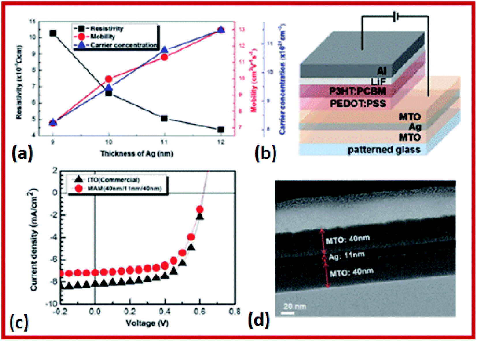 | ||
| Fig. 11 (a) Electrical properties of MTO/Ag/MTO films. (b) Schematic of conventional BHJ-OPV having the MTO/Ag/MTO multilayer electrode. (c) Current–voltage characteristics of the optimized MTO/Ag/MTO multilayer and ITO as reference based on OPVs. (d) TEM (cross-section) for the MTO/Ag/MTO multilayer electrode,209 reproduced with permission and copyright. | ||
5. Impact of SnO2 based TCO and ETL on OPV and OLED devices
5.1 Impact of SnO2 on OLED devices
A typical OLED consists of an anode deposited on a glass substrate, one or more charge transport and light emitting layers and a low work function cathode. Under an external bias, the holes and electrons are injected from the anode and the cathode, respectively, through a transport layer into the emitting material as the recombination generates excitons. These excitons activate the light emitting material to emit photons (light) because of the radiative recombination. Transparent materials are more favorable for these OLED devices. In particular, SnO2 as an n-type TCO is a good choice of material for different components in OLEDs.Indium-free SnO2 may also be a promising electrode material because of its high transparency and large bandgap. More importantly, the fabrication of SnO2 is compatible with many techniques. M. Esro et al.97 demonstrated that the Sb-doped SnO2 (SnO2:Sb) deposited through a facile low-cost spray pyrolysis technique is a promising anode material for large-scale and flexible OLEDs. By varying the Sb concentrations, at 2 wt%, the SnO2:Sb film exhibits the lowest sheet resistivity and the highest electron mobility. The SnO2:Sb (2 wt%) shows a similar surface roughness in comparison with the commercially available ITO anode. Regarding the optical properties, such as making of red, green, and blue OLED devices, the energy level alignment comparison shown in Fig. 12a–c indicates that the SnO2:Sb anode has a lower work function than that of ITO, which is favorable for the hole injection. The three different-color OLED devices deposited on the SnO2:Sb anode show comparable electrical and optical performances with those deposited on ITO. These results clearly indicate the great potential of the Sb-doped SnO2 electrode in flexible and large-scale OLEDs fabrication.
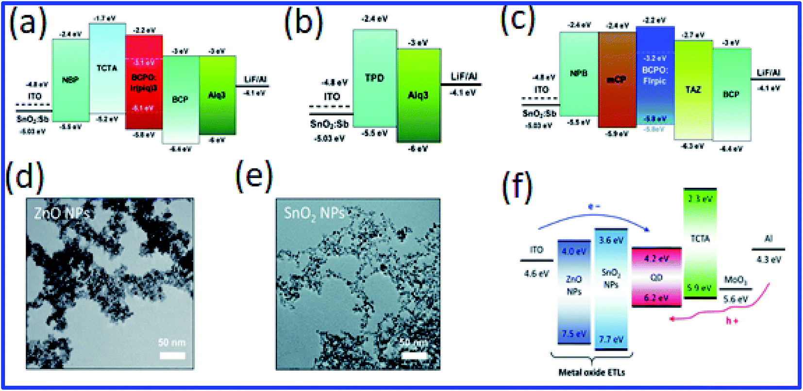 | ||
| Fig. 12 Energy band diagrams of (a) red, (b) green, and (c) blue OLEDs with SnO2:Sb or ITO as the anode electrode. Reproduced with permission.97 Copyright: The Royal Society of Chemistry 2016. The TEM images of (d) ZnO or (e) SnO2 NPs; (f) energy level diagram of QD-LEDs with ZnO or SnO2 NPs as the ETLs. Reproduced with permission.213 Copyright: The Royal Society of Chemistry 2020. | ||
Currently, SnO2 is one of the best electron transporting materials (ETMs) in perovskite solar cells because of its excellent electron mobility; therefore, it is being introduced into other related devices as an ETL. Park et al.213 investigated colloidal quantum dot LEDs (QD LEDs) because of their tunable emissive light with pure color and very high photoluminescence quantum yield (almost reaching 100%). In the QD LEDs, ZnO is the widely used ETM; however, it often allows more electrons to be transported to the QD emissive layer, causing a hole–electron imbalance. This is also the main barrier for high-performance and stable QD LEDs. Park et al.213 compared the properties of SnO2 as the ETM with those of ZnO. Transmission electron microscopy (TEM) and atomic force microscopy (AFM) images indicate that SnO2 NPs have a similar size (Fig. 12d and e) to that of ZnO NPs but a smoother surface, which allows better layer-by-layer connection. Both SnO2 and ZnO NPs have a similar electron mobility in OFETs; however, the carrier concentration of ZnO is more than two times higher than that of SnO2, which will cause excessive electron injection, leading to imbalance with holes. SnO2 NPs, however, exhibit lower carrier concentration but the same electron mobility, indicating the excellent transporting ability to balance the holes to result in improved device performance. Although the LUMO of SnO2 NPs is slightly higher than that of ZnO NPs (Fig. 12f), the overall QD LED device performance with SnO2 NPs is higher than that of the device with ZnO NPs, including a lower turn-on voltage, higher maximum luminance, improved EQE roll-off property and better power efficiency.
Another example about SnO2 as the ETM is reported by Hong et al.214 where they studied the difference in the OLED device performance caused by the relative position of SnO2 and the organic emitter (copper phthalocyanine, CuPc). Two devices were fabricated with different layer-by-layer structures, as shown in Fig. 13a and d. In the normal device, CuPc is deposited on top of SnO2 (CuPc-on-SnO2, Fig. 13e), while in the inverted device, the SnO2 is deposited on top of CuPc (SnO2-on-CuPc, Fig. 13b). Because of the much higher melting temperature of SnO2, the hot Sn atoms during deposition on top of CuPc will cause a breakdown of the weak bonds that existed in CuPc, resulting in a chemical reaction to form CuPc–Sn. Therefore, its charge distribution is changed compared with that of the pristine CuPc, which results in the increment in both the interface dipole and hole injection barrier (Fig. 13c). If the SnO2 is first deposited, the low processing temperature of CuPc will not provide sufficient energy for the formation of the condensation reaction (CuPc–Sn). In this case, it avoids those negative effects that occurred in the SnO2-on-CuPc structure (Fig. 13f). The device performance with CuPc-on-SnO2 is found to be better in terms of both the operating voltage and the luminance than that of the device with the SnO2-on-CuPc structure.
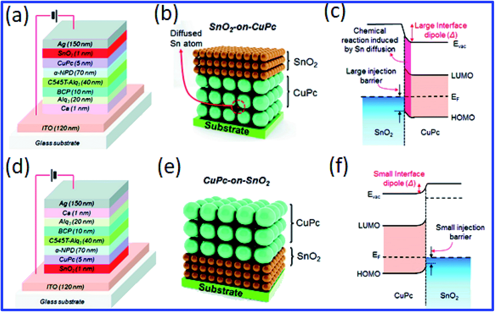 | ||
| Fig. 13 Device structures of (a) normal OLEDs and (d) inverted OLEDs. (b and e) Schematic diagram and (c and f) energy band structure of the (b and c) diffused SnO2-on-CuPc and (e and f) abrupt CuPc-on-SnO2 interface. Reproduced with permission.214 Copyright: American Chemical Society 2011. | ||
For many organic devices, interface modification is an effective way to improve the device performance. Taking that into consideration, Lee et al.215 applied SnO2 NPs as an interface layer between the ITO cathode and the ETL in an inverted bottom-emission (ITO direction) OLED device. The work function of SnO2 nanoparticles was found to be between the ITO and the ETL. That was helpful to form a ladder-like energy alignment from ITO to the emitter to facilitate the electron injection. Additionally, the SnO2 film morphology spin-coated from 3 wt% aqueous solution was found to be the smoothest, which is favorable for establishing contact with the ETL and the electron transport, delivering more electrons to the emitter layer to balance the holes injected from the anode. The performance measurement of the OLED device indicates that the operating voltage to achieve 1000 cd m−2 luminance decreased significantly from 24.0 V (without SnO2) to ∼17.0 V (with SnO2) with an enhanced EQE from 8.2% to 15.6%.
These samples clearly indicate that, to get the best performance, the properties of SnO2 should be carefully considered; for example, the work function, film morphology, and processing method. Successful cases are given above by applying SnO2 in different layers of the device to fulfill specific roles. Therefore, in future research, to better incorporate SnO2 in OLEDs, the relationship between SnO2 and the neighbour layers should be carefully studied to realize optimized charge carrier transport.
5.2 Impact of SnO2 on OPV devices
The OPV device has two types of generic structures: a conventional structure and an inverted structure. The basic geometry of the conventional device has continuous layers of ITO (anode)/PEDOT:PSS/active layer/metal (cathode). Such a structure is unfavorable for device stability which is one of the three most crucial factors for OPV commercialization. The other two are the power conversion efficiency (PCE) and scalability. Therefore, an inverted device geometry with a general structure of ITO (cathode)/metal oxide/active layer/metal (anode) is developed in which metal oxide is used as the electron transporting layer deposited on top of the ITO cathode. Compared with the conventional device where PEDOT:PSS is deposited on top of the ITO anode,216–222 the stability of the inverted device is improved since the metal oxide will not erode the ITO as the acidic PEDOT:PSS (pH: 1–2) does. Besides, the metal oxide will also protect the active layer from oxygen and humidity.223,224 Moreover, the cathode in the conventional devices is generally of low-work-function metals, such as aluminium (Al) and calcium (Ca). These metallic cathode materials are easy to oxidize and even further hydrolyze in an ambient atmosphere. In the inverted device, however, the metals used as an anode are high-work-function materials, such as Ag and Au, which have higher work functions than those of Al and Ca. Because of this concern, the device engineering is mostly focused on inverted devices. Although the active layer materials play significant roles in improving the device performance, there are also many possibilities in judicially selecting suitable materials in the metal oxide layer. Currently, the widely used metal oxides in the ETL are TiO2 and ZnO. That is mainly because of their high transparency and suitable work function. However, there are some disadvantages, such as the low electron mobility of TiO2, the instability of both TiO2 and ZnO and the high-temperature processing conditions of TiO2. All these motivate the development of alternative materials for the electron transporting layer. SnO2 is one of the best electron transporting materials in perovskite solar cells because of its high transparency, ultrahigh electron mobility (>200 cm2 V−1 s−1), non-light-soaking problems, and high chemical, photo-stability and hole blocking properties.225 Despite these favorable features for efficient electron transport, the application of SnO2 in OPVs is rare. One reason is that the trap-assisted recombination at the SnO2 surface is severe and requires surface modification to enable its compatibility with the organic blends in the active layer of OPV devices.An example of the comparison of SnOx with TiOx and ZnO as the electron extraction/transporting material was reported by Trost et al.226,227 One of the advantages of SnOx as the ETM is demonstrated, i.e., the light-soaking issue faced by TiOx and ZnO is not a problem in SnOx ETM-based OPV devices. Light soaking is defined as the activation of TiOx and ZnO by UV light to make the resultant devices show good performance. However, the activation will take some time to finish, and in the meantime, the organic donor materials in the active layer may degrade under UV light illumination. Therefore, UV light protection is very much necessary for OPV devices. As shown in Fig. 14a and b, without UV light activation (filtered AM 1.5), a sigmoidal J–V curve is observed in TiOx ETM-based inverted OPV devices with an inferior efficiency of 0.4%. However, the SnOx ETM-based device shows a largely enhanced efficiency of 5.7%. Although the exact reason for the light-soaking issue has not been clarified, it is an acceptable concept that the UV light activation induces oxygen desorption on the TiOx/ZnO surface that causes the decrement of work function for better electron extraction/transport. For the SnOx film, UV light illumination does not change its work function much. This, combined with its suitable value, allows better performance to be achieved for SnOx ETM-based inverted OPVs.
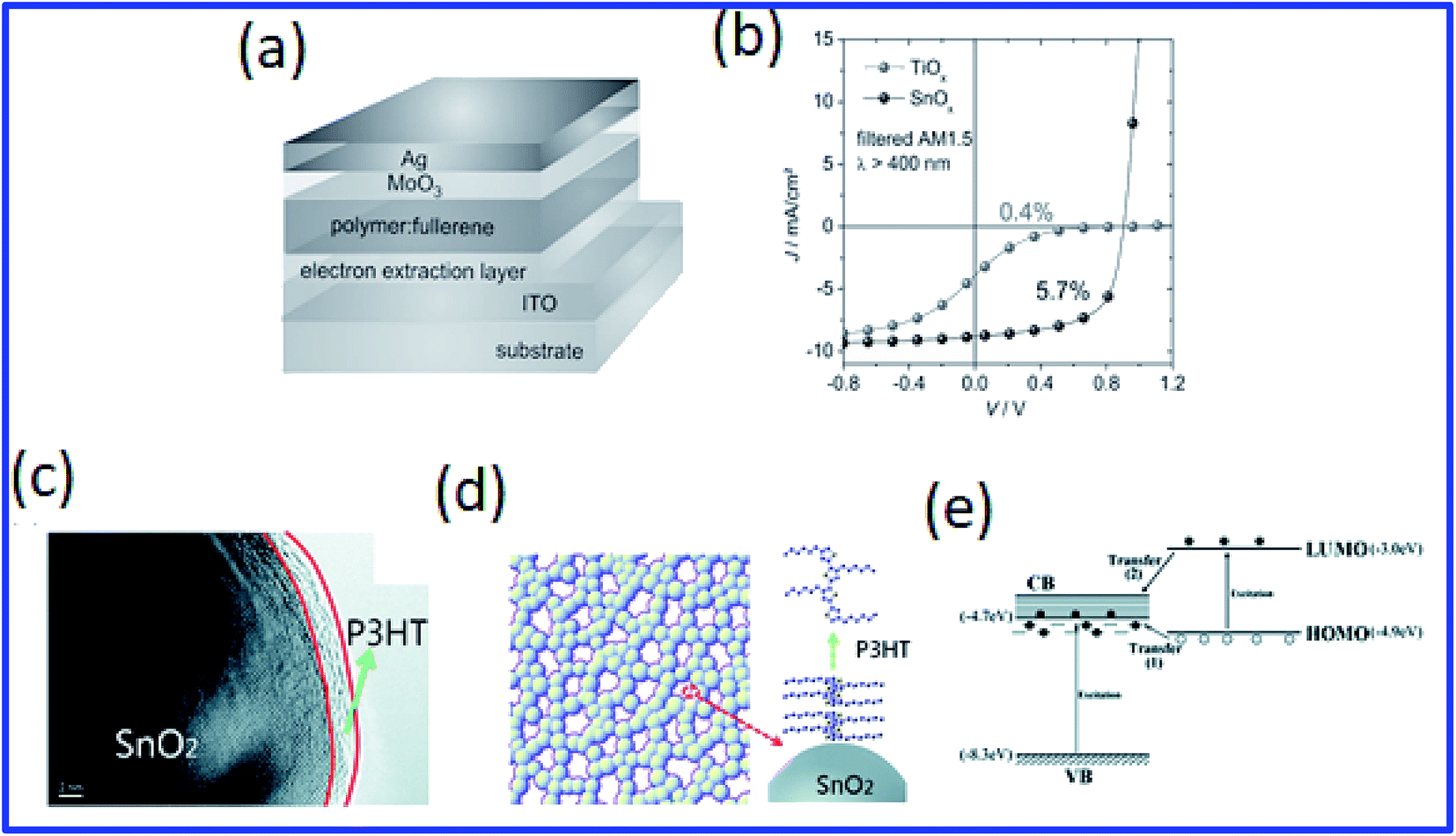 | ||
| Fig. 14 (a) Layer sequence of the inverted OPV device with TiOx or SnOx as electron extraction layers and (b) J–V characteristics of the corresponding cells under AM 1.5G illumination with a UV blocking filter (λ > 400 nm). Active layer: PCDTBT:PC71BM. Reproduced with permission.226 Copyright: WILEY-VCH Verlag GmbH & Co. KGaA, Weinheim 2015. (c) HRTEM image of a SnO2 nanocrystal covered with a P3HT thin layer. (d) Schematic structure of the P3HT–SnO2 composite semiconductor. (e) Energy level alignment of P3HT and SnO2. Reproduced with permission.228 Copyright: The Royal Society of Chemistry 2016. | ||
Although the light-soaking issue is resolved in SnOx ETM-based inverted OPVs, as mentioned above, the charge traps and charge recombination exist on the SnOx surface. Therefore, surface modification is required to avoid these traps and improve the performance of the inverted OPVs. Geng et al.228 investigated the preparation of a SnO2 and poly(3-hexylthiophene) (P3HT) composite. Although this composite is not used in OPV devices, this study confirmed that the SnO2 surface modification generates favorable properties in charge carrier transport. On the surface of SnO2 nanoparticles, highly crystalline domains are favorable for charge carrier transport. However, the porous network restricts further improvement in mobility. The semicrystalline P3HT is used as a filler in the porous structures of SnO2 nanoparticles, forming a P3HT–SnO2 composite, as shown in Fig. 14c. After thermal annealing, the electron transfer inside the composite is promoted because of two reasons. First, the chemical bonds formed between SnO2 and P3HT, combined with the highly crystalline feature of P3HT, is responsible for the electron transfer from P3HT to SnO2 (Fig. 14d and e), resulting in more free charges in SnO2 nanoparticles. Second, thermal treatment in a high-pressure oxygen atmosphere for SnO2 allows for elimination of oxygen vacancies to increase the crystallinity of SnO2. The synergistic effects of more free charges and high crystallinity of the SnO2 section in the P3HT–SnO2 composite contribute to the higher electron mobility than those of pristine P3HT or SnO2 film. This work elegantly demonstrates the feasibility of surface modification of SnO2 to promote its application as an electron transporting material in inverted OPVs.
Shen et al.64 reported that a (poly-[(9,9-bis(3-(N,N-dimethylamino)propyl)-2,7-fluorene)-alt-2,7-(9,9-dioctylfluorene)]), PFN, layer deposited on the SnO2 film can adjust the energy level and reduce the surface defects. Such a bilayer, SnO2/PFN, as the electron transporting material in inverted OPVs (ITO/SnO2/PFN/PTB7-Th:PC71BM/MoO3/Ag, Fig. 15a) greatly enhanced the efficiency from 4.31% (pristine SnO2) and 9.05% (pristine PFN) to 11.05% (Fig. 15b). Two main aspects are improved for the bilayer, SnO2/PFN, compared with the pristine SnO2 and PFN. First, the work function of pristine SnO2 is significantly reduced from 4.46 eV to 3.9 eV because of the dipoles formed on the PFN surface. This significantly reduced work function helps in achieving step-by-step energy level alignment of the device, facilitating electron transport. Furthermore, the transient photovoltage and photocurrent decay curves indicate that the photo-induced electrons can be extracted to the ETL and the lifetime can be extended (Fig. 15c and d). This demonstrates a better extraction capability and a lower charge recombination rate in SnO2/PFN compared with both the pristine SnO2 and PFN layers.
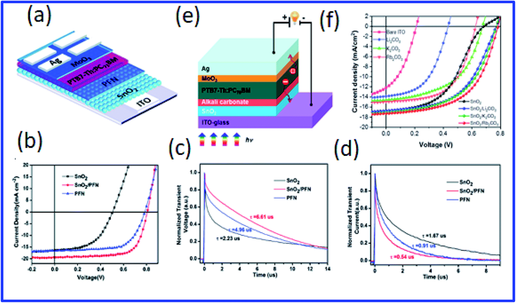 | ||
| Fig. 15 (a) Device structure of the inverted OPVs by integrating low temperature solution-processed SnO2 nanocrystals and a PFN stacked structure as an ETL. (b) J–V characteristics of SnO2-only, SnO2/PFN, and PFN-only devices tested under AM 1.5G in ambient air. (c) Transient photovoltage and (d) transient photocurrent decay curves based on SnO2 and SnO2/PFN and PFN ETLs. Reproduced with permission.64 Copyright: The Royal Society of Chemistry 2018. (e) Device structure of the inverted OPVs using SnO2 or SnO2/alkali carbonates as ETLs and (f) the J–V characteristics under standard AM 1.5G. Reproduced with permission.225 Copyright: American Chemical Society 2018. | ||
Similar results are also found in zwitterion compound-modified SnO2 films, as reported by Tran et al.229 The synergistic effects of aligned energy levels and improved electron extraction and transport contribute to the significantly enhanced efficiency of inverted OPVs. Tran et al.225 also reported similar results by selecting alkali carbonates (lithium carbonate, Li2CO3; potassium carbonate, K2CO3; and rubidium carbonate, Rb2CO3) to modify the SnO2 surface (Fig. 15e). The reason to choose alkali carbonates is because of their good electron-transporting property but poor hole blocking property. Apart from the enhanced device performance (Fig. 15f), the stability of the unencapsulated device is observed to be very high, maintaining >90% of efficiency even after 6 weeks. This stability is because of the inverted device structure and the use of SnO2 as the electron transporting material. The comparison of the stability of devices with SnO2 or ZnO as the electron transporting material has been reported by other groups of researchers.230
In the field of OPVs, non-fullerene acceptors have gained increasing attention recently. Jiang et al.230 fabricated inverted non-fullerene OPV devices with the structure of ITO/SnO2 or ZnO/PM6:IT-4F/molybdenum oxide/silver (ZnO/PM6:IT-4F/MoO3/Ag) in which ZnO or SnO2 is used as the electron transporting material. The device stability study under continuous AM 1.5G illumination indicates that the device fabricated with ZnO displays a dramatic drop in efficiency from 13.0% (initial) to 5.1% (after 24 hours), while the device fabricated with SnO2 exhibits a consistent efficiency with slight variation from 14.1% (initial) to 12.5% (after 24 hours). It is observed that after 24 hours of illumination, the ZnO/IT-4F film on glass decomposed, while the pristine IT-4F and SnO2/IT-4F films remained the same. The reason is that the photocatalytic effect of ZnO caused the decomposition, whereas SnO2 has a wide bandgap that does not allow the absorption of photons, avoiding the photocatalytic effect to cause the decomposition of the active layer material. Meanwhile, an important characteristic of SnO2-based inverted non-fullerene devices is that the efficiency is independent of thermal annealing treatment with a high value of >12% at room temperature. This can pave the way for its commercialization in the future.
Another example of inverted non-fullerene OPV with modified SnO2 is reported by Peng et al.,231 where InP/ZnS (indium phosphide/zinc chalcogenide) quantum dots are used to passivate the surface defects of SnO2. The reasons for the selection of quantum dots include the following two aspects: (1) the water/alcohol solubility allows a good connection with both SnO2 and the organic active layer and (2) the small size allows distribution into the SnO2 film to passivate the SnO2 surface defects. After modifying with InP/ZnS quantum dots, studies indicate that the transmittance of the device does not change much, which ensures the photon harvesting property. The morphology of the active layer is improved, which is desirable for yielding high JSC (short-circuit current). Higher SCLC (space-charge-limited current) mobility favors the FF (fill factor) increment. Semi-logarithmic plots of J–V curves indicate the increased breakdown voltage and slope of the device, which is the origin of higher open circuit voltage (VOC). The efficiency of the SnO2/InP/ZnS-based device (ITO/SnO2/InP/ZnS/PM6:Y6/MoO3/Ag) thus reaches a very high value of 15.22%, which is even one of the best efficiencies in non-fullerene OPVs.
An interesting idea is to utilize perovskite nanowires to modify the SnO2 surface to act as the ETL in non-fullerene OPVs. In this context, Zhao et al.232 did the same work where MAPbI3 nanowires are introduced on top of SnO2 to make it more compatible with the organic blends in the active layer of the device with the structure of ITO/SnO2/MAPbI3 nanowires/PBDB-T-SF:IT-4F/MoO3/Ag. Although the efficiency has only a slight increment from 9.53% (SnO2 only) to 10.72%, an interesting phenomenon is that the MAPbI3 bulk film-containing device shows only a half efficiency of 5.52%. These results indicate that a suitable perovskite structure can modify the SnO2 and improve the compatibility with the organic blends in non-fullerene OPVs. Therefore, future work on this may be meaningful to improve the efficiency of devices containing both perovskite and non-fullerene active layers for potential commercialization.
These results indicate that the surface modification of SnO2 is an effective strategy for the improvement of OPV device efficiency and stability. Looking for an appropriate material to modify the SnO2 surface is one of the directions for its better use in OPVs. Device efficiency and stability are two of the three crucial parameters (another one is the cost) for OPV device commercialization; therefore, finding a low-cost material to effectively modify SnO2 to improve the device efficiency and stability will greatly pave the way for the future commercialization.
6. Boosting the perovskite performance and stability through SnO2
6.1 SnO2 as the TCO and the ETL for perovskite solar cells (PSCs)
Metal-halide perovskite thin-film solar cells are typically fabricated using commercial fluorine-doped tin oxide glass as substrates. Although these substrates have low sheet resistance Rs (8–20 Ω cm2), the RMS surface roughness is high (5–20 nm). Besides, the FTO morphology leads to pinholes in the carrier transport layers. In a study that focused on both FTO and TiO2 blocking layers, Yates et al.233 deposited FTO by atmospheric pressure CVD (APCVD) using monobutyl tin trichloride (MBTC) as a tin precursor and aqueous trifluoroacetic acid (TFAA) as the dopant, where two samples with similar sheet resistances but different surface roughness values were deposited by using different deposition thicknesses. For the polycrystalline FTO film, the surface roughness varies with film thickness and develops various crystallographic planes at different rates. Perovskite solar cells (PSCs) with the mesoscopic structure of FTO/TiO2−x/m-TiO2/CH3CH2PbI3/spiro-OMeTAD/Au were fabricated using the two types of APCVD FTO and commercial FTO glass substrates. The interesting observation was that even though the commercial FTO (Solaronix TCO22-15) has a lower sheet resistance and a higher carrier mobility, devices fabricated on commercial FTO substrates exhibited lower PCE than those fabricated on APCVD-grown FTO substrates. This difference was attributed to the reduction of optical transmission due to increased absorption by free carriers of transparent electrode layers. The higher surface roughness of APCVD FTO yields slightly higher PCE because of increased internal light scattering.To gain a deeper insight into the effect of the TCO layer on PSCs, Afzaal et al. used APCVD to deposit FTO films with different thicknesses and a fixed resistance (Rs) as well as different Rs values for the same thickness.235 Mesoscopic PSC thin-film solar cells (1 cm × 1 cm) with the structure FTO/TiO2−x/CH3CH2PbI3/spiro-OMeTAD/Au were fabricated on APCVD-grown FTO substrates. It was found that increasing FTO thickness has a clear and significant effect on the PCE of the devices due to the correlation between the FTO film thickness and its surface roughness. Samples with thicker FTO layers but the same Rs show improved FF and reduced VOC and JSC. When Rs increased, with the thickness remaining the same, both VOC and JSC increased, but FF was reduced. For the optimized FTO deposition, a PCE of 17.8% was achieved, higher than that of the reference device fabricated on commercial FTO substrates. This study demonstrates that careful tailoring of the optical, structural, and electronic properties of FTO is necessary to obtain the enhanced performance of PSC devices. SnO2 and different metal-doped SnO2 are used as the electron transport layer (ETL) in planar PSCs. Different approaches such as the atomic layer deposition (ALD) technique, solution-processing method, and the CBD technique have been adopted for the preparation of this SnO2 based ETL. Baena et al.234 reported planar PSCs using SnO2 and TiO2 as ETLs and they found that, for planar PSCs, SnO2 was much more effective than TiO2. They claimed that SnO2 has a much more favorable conduction band alignment with the MAPbI3 and mixed (FAPbI3)0.85(MAPbBr3)0.15 perovskite absorber, which yielded a much higher PCE as shown in Fig. 16a–d, using SnO2 as the electron selective layer. In this report, the ALD technique was used to prepare the SnO2 layer on the top of an FTO substrate. In parallel, Ke et al. also reported a planar MaPbI3 PSC using solution-processed SnO2 as the ETL.236 They prepared SnO2 by facile spin coating of the SnCl2·2H2O precursor prepared at room temperature, followed by thermal annealing in air at 180 °C for 1 h. The mild annealing conditions resulted in a smooth nanocrystalline SnO2 ETL which covers the FTO substrate and improves its optical transmittance. They achieved high performance planar PSCs with a forward scan PCE of 14.82% and a reverse scan efficiency of 17.21%. After that several groups had reported planar PSCs based on SnO2 as the ETL.53,237–240 Different approaches were made for optimizing the SnO2 layer as the ETL to boost the performance of the PSCs. Among these approaches, the most effective approaches are doping of SnO2 using different metals such as aluminium (Al), antimony (Sb), lithium (Li), and tantalum (Ta);56,241,242 high temperature annealing;243 use of different additives such as ethylenediaminetetraacetic acid (EDTA)65 and 2,2,2-trifluoroethanol in SnO2;244 and an additional ETL such as PCBM239 or In2O3 together with the SnO2 layer.240 With all these approaches, the device performance could be significantly improved.
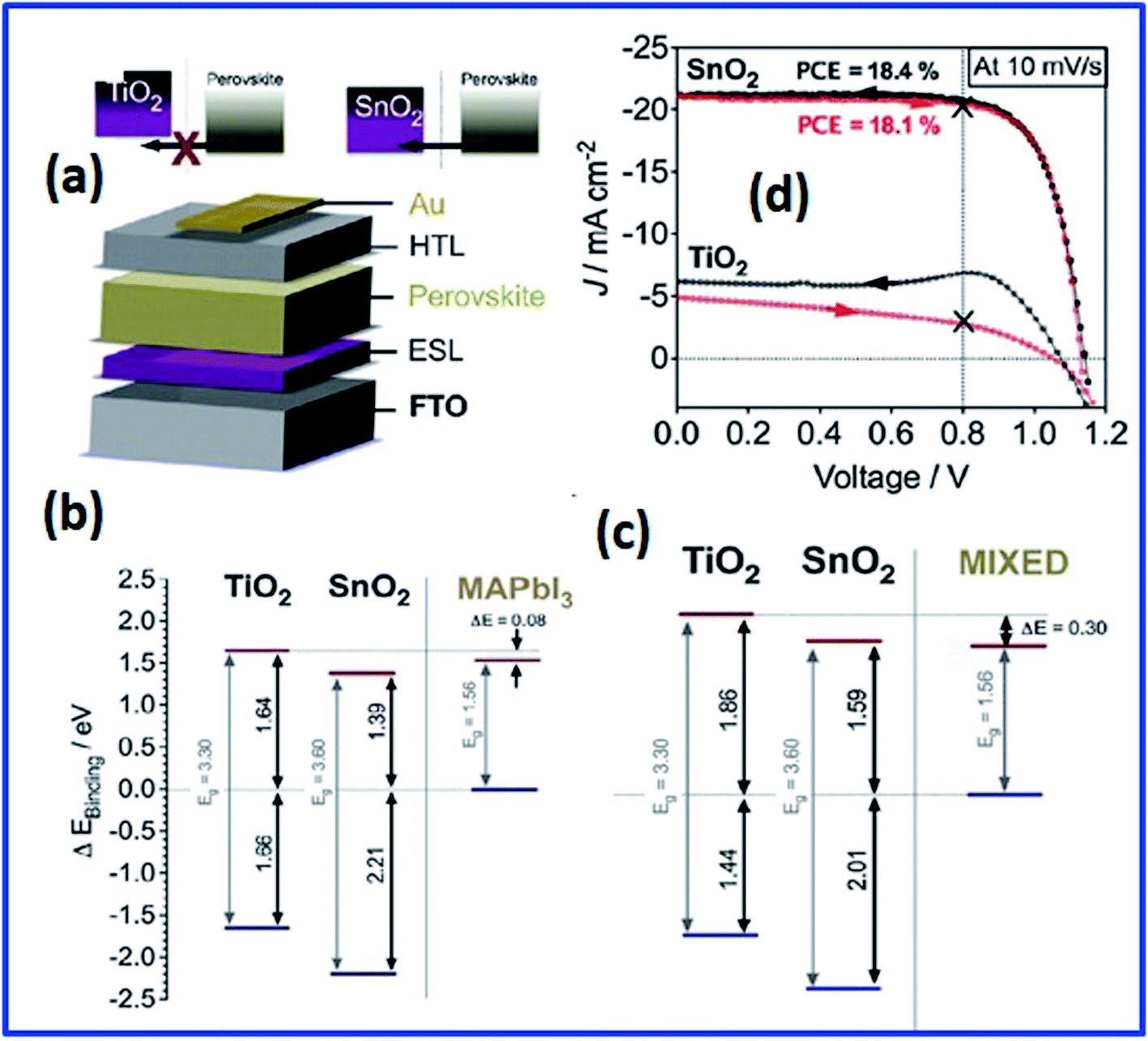 | ||
| Fig. 16 (a) Energy level diagrams and electron injection characteristics of SnO2 and TiO2-based planar PSCs. Schematic conduction band diagram of the perovskite films and the electron selective layers (ESL), TiO2 and SnO2 for (b) MAPbI3 and (c) (FAPbI3)0.85(MAPbBr3)0.15, labeled as ‘mixed’. (d) Current–voltage characteristics of planar perovskite devices based on SnO2 and TiO2 ESLs,234 presented with permission and copyright. | ||
Although the PCE of present perovskite thin-film solar cells is well over 20%, the J–V characteristics of these devices are scan direction-dependent and show considerable hysteresis.245,246 Earlier, this phenomenon was thought to be due to charge accumulation effects at the TiO2/perovskite interface where TiO2 is the default electron transport layer (ETL).245 To eliminate the hysteresis, interfacial layers based on fullerene derivatives have been inserted between the ETL and the perovskite layer.238,246 The hysteresis behavior in J–V characteristics is also a burden in the case of SnO2 as the ETL. Recently, Jung et al. employed a sol–gel method to deposit the SnO2 ETL onto FTO substrates using tin(IV) isopropoxide as the precursor.243 The process parameters investigated include the tin precursor concentration and post-deposition annealing temperatures. The thermal annealing was in addition to the heating in a N2 glovebox environment that was intended for drying the deposited layer. The SnO2 ETL annealing temperature in the range of 100 °C to 500 °C has a significant effect on lowering the hysteresis of the J–V profiles. From 100 °C to 250 °C, the hysteresis between the forward and reverse J–V scans decreases and then increases again from 250 °C to 500 °C. Annealing at 250 °C was found to be more effective as the ultraviolet photoelectron spectroscopy (UPS) study showed a better band alignment with the electrode (Fig. 17a). At 250 °C, the PV parameters for the forward and reverse scans were almost the same. An average PCE of 16.08% was achieved for a precursor concentration of 0.1 M (Fig. 17c), and this was further improved to 19.17% with the incorporation of potassium in the perovskite (Fig. 17d). The greatly reduced hysteresis was attributed to both a reduced interfacial capacitance and faster stabilization of the photocurrent. PSCs with mixed cation and anion absorbers with the device geometry of FTO/SnO2/(FAPbI3)0.873(CsPbBr3)0.125/spiro-OMeTAD/Au (Fig. 17e) were fabricated. The effect of precursor concentration for SnO2 films annealed at 250 °C was also studied,243 which mainly influenced the thickness of the spin-coated layer. By varying the annealing temperature and the precursor concentration, the hysteresis area under the forward and backward J–V curves was eliminated (Fig. 17c and d). For concentrations above and below the optimal value of 0.1 M, there was significant hysteresis and the hysteresis was the largest for controlled devices where the SnO2 layer was not used (Fig. 17b). For the low concentration of the precursor, the hysteresis was ascribed to the poor surface coverage of the FTO substrate, while for high concentrations, the hysteresis was due to the increased series resistance. This study highlights the importance of post-deposition annealing of SnO2 ETL in eliminating the hysteresis phenomenon in the J–V characteristics of perovskite solar cells.
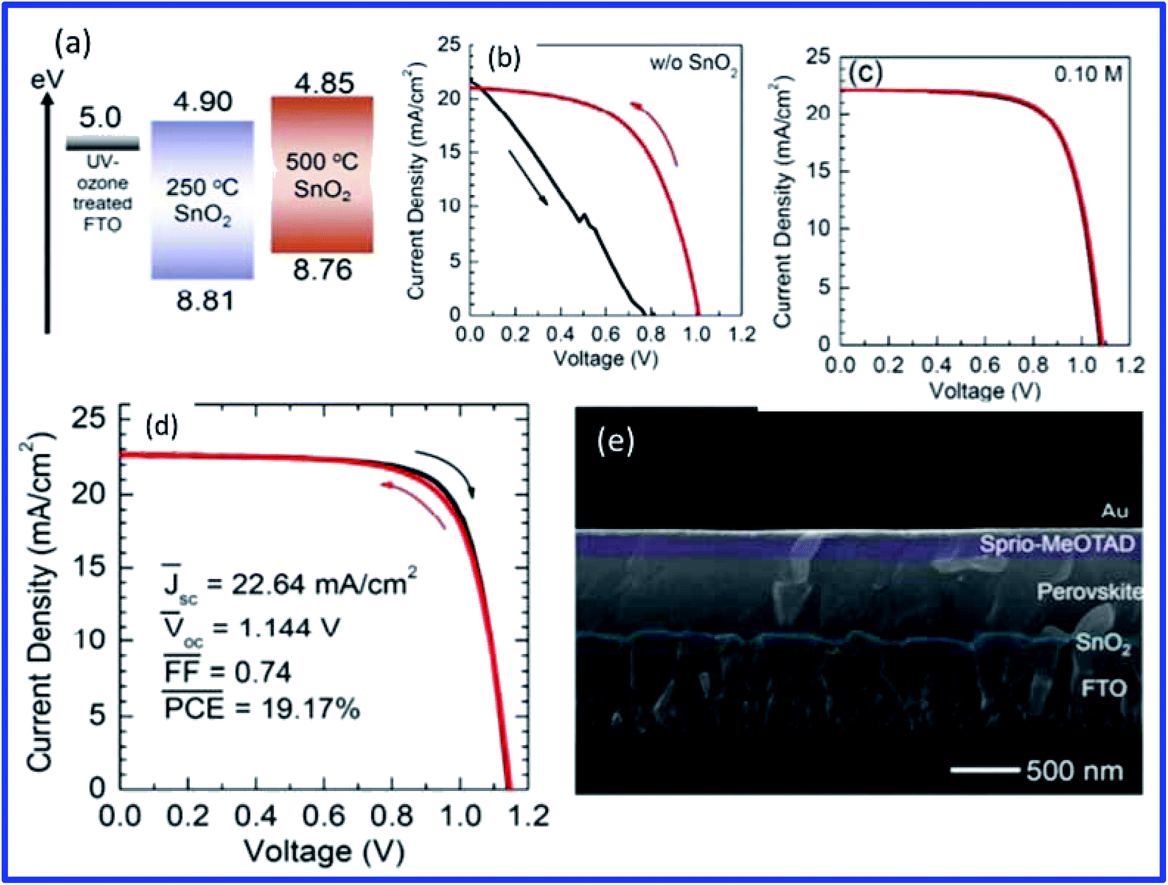 | ||
| Fig. 17 (a) Schematic of energy alignment of the UVO treated FTO and SnO2 films annealed at 250 °C and 500 °C. Reverse (red) scan and forward (black) scan J–V curves of planar perovskite solar cells (b) without and (c) with SnO2 thin films prepared from 0.1 M concentration of the SnO2 precursor solution. (d) J–V curves and (e) cross-sectional SEM image of the best performing planar perovskite (with potassium doped) solar cell employing the 0.1 M-based and 250 °C-annealed SnO2 thin film with a thickness of ∼40 nm,243 presented with permission and copyright. | ||
It was also found that the low open-circuit voltage (those with a bandgap of between 1.59 and 1.63) originates from electron collecting layers (mainly oxide nanocrystal thin films) used as transparent electrodes. A well-matched energy band between the ETL and perovskites improves VOC by avoiding the excessive band offset while accelerating the charge carrier extraction, resulting in efficient transport. In this regard, very recently, Wang et al.240 reported a unique work based on gradient energy alignment engineering using the In2O3/SnO2 bilayer as the ETL and found a negligent extent of hysteresis loss in VOC. Deposition of a very thin layer of Li on the SnO2 layer as the ETL was also found to be very effective for proper band alignment and to reduce surface defects at the interface in the case of all inorganic perovskite CsPbI3−xBrx solar cells (Fig. 18a–c).239 Low-temperature solution-processed SnO2 nanoparticles were also found to be very efficient as the ETL for planar perovskite solar cells on a rigid substrate and a flexible PET substrate (Fig. 18d and e).247
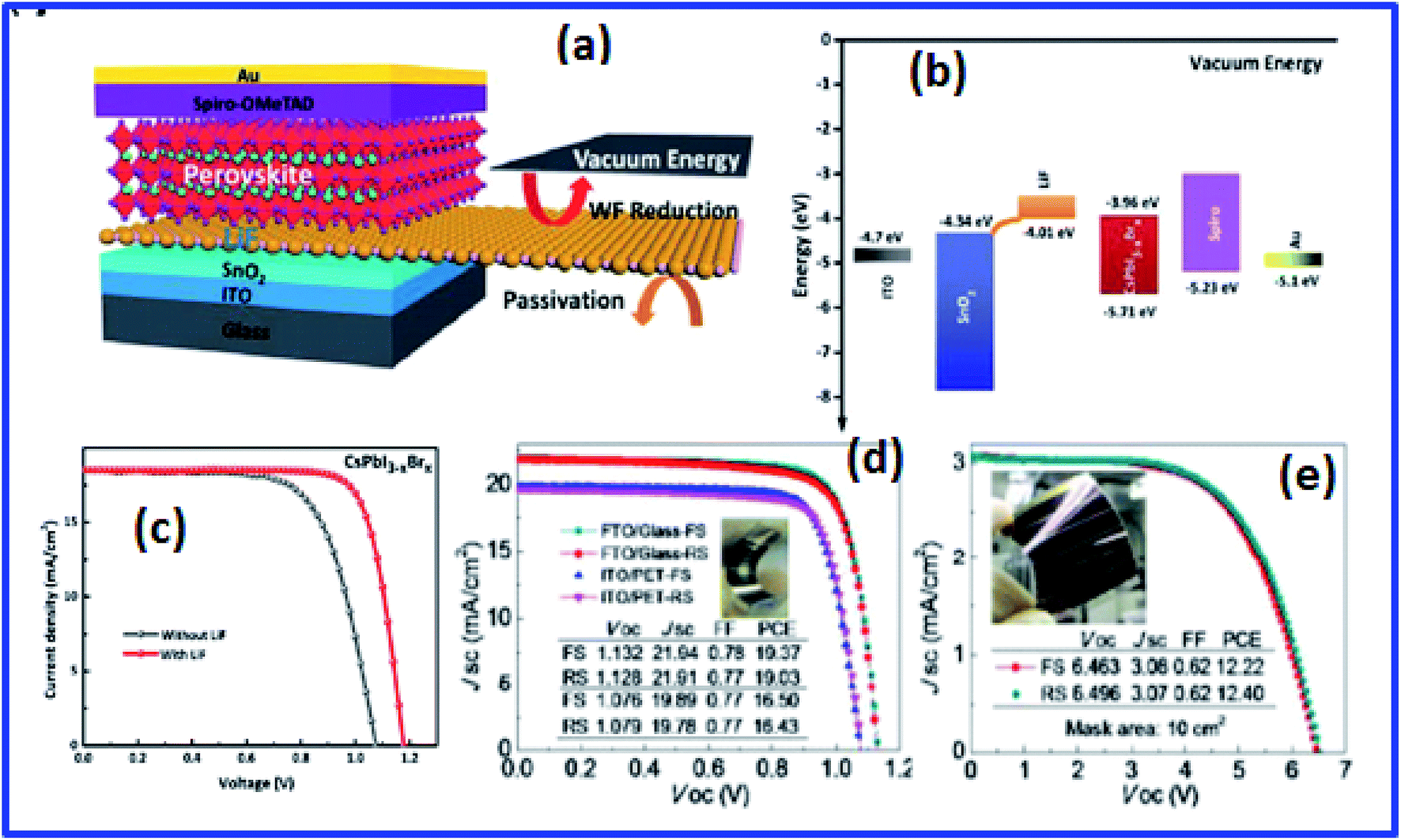 | ||
| Fig. 18 (a) Scheme of the device architecture of the inorganic perovskite solar cells; LiF was used to modify the SnO2 surface. (b) Energy band alignment for each layer in CsPbI3−xBrx inorganic solar cells. (c) J–V characteristics of inorganic CsPbI3−xBrx solar cells with and without the LiF interlayer.239 (d) Hysteresis-free perovskite devices on glass and PET substrates and (e) flexible perovskite module of the same devices by chemical treatment of the SnO2 layer,247 presented with permission and copyright. | ||
The use of the SnO2 layer on a CVD-/sputter-grown FTO substrate could broaden the optical transmission band of the electron selective layer and fill electronic states in the conduction band of the perovskite film resulting in the enhancement of charge concentration in quasi-Fermi energy levels at ETL–perovskite interfaces. Solution-processed Al/F/Sb-doped tin oxide coating is a feasible way to produce transparent conductive substrates and electron transport layers in a single process that will be crucial for developing hysteresis-free high-performance PSC (PCE = 16–20%) modules on the industrial scale.247
6.2 Impact of SnO2 on flexible PSCs
Since the first report of flexible PSCs with a PCE of 2.62% by Mathews' group in 2013,248 the PCEs of the flexible PSCs have increased to 18.5%.249,250 Progress of the flexible PSCs was based on different functional layers, which have been prepared by different low temperature process technologies. In this regard, SnO2 was found to be very effective as the ETL, which has been prepared by different techniques such as solution-processing, room temperature sputtering, ALD and slot-die printing. Dong et al.63 reported the in situ regrowth of the SnO2 layer by pretreating the substrate by ultraviolet ozone (UVO). This UVO treatment helped the substrate to adsorb the optimum amount of water molecules which facilitates hydrolysis–condensation reactions for the regrowth of the spin-coated SnO2 NPs. With this deposition technique of the SnO2 as the ETL, the authors reported a PCE of 17.5% for a flexible PSC.63 Qiu et al.251 reported a two-step solution-processed SnO2 layer formation by depositing a layer of SnCl2 on the spin-coated layer of SnO2 NPs. This SnCl2 layer helped to improve the quality of the ETL through hydrolysis and oxidation of SnCl2. They have reported the device efficiency of 15.21% for the flexible PSC devices, with prolonged shelf-stability.251 Liu et al.252 also reported two-step techniques to deposit the SnO2 layer. After depositing a SnO2 NP aqueous solution on an ITO/polyethylene naphthalate, PEN substrate by spin coating, they treated the film by the hydrothermal technique using an autoclave at 100 °C for 1 h, and a significant improvement of the quality of the SnO2 layer was obtained. They achieved a certified efficiency of 17.27% for the flexible PSCs. The authors concluded that the enhanced performance of the PSCs can be attributed to the large grain sizes of the perovskite on hydrothermally treated SnO2, low trap density of the device, high charge transport efficiency of hydrothermally treated SnO2, and the better energy band matching between hydrothermally treated SnO2 and the perovskite layer.252 In most of the reports, spin coating of an aqueous solution of SnO2 NPs followed by some kind of treatment have been used for a better quality of the SnO2 layer. The work by Yang et al.65 revealed that by preparing a complex of SnO2 aqueous solution with EDTA, an effective ETL can be formed. It has been found that this EDTA-complexed SnO2 is better matched with the conduction band of perovskite, leading to high VOC. Its electron mobility is about three times larger than that of SnO2. Using EDTA-complexed SnO2, the group has reported an efficiency of 18.28% for a flexible device.65 Similarly, Kam et al.31 reported room-temperature RF sputtered SnO2 as a promising ETL with a suitable band structure, high transmittance, and excellent stability for the PSCs. They achieved PCEs of 12.82% and 5.88% on a rigid glass substrate and a flexible PEN substrate, respectively.31 Another non-solution based process which has been reported for the formation of the SnO2 layer is the slot die coating. The approach towards flexible perovskite solar cell modules (PSCMs) was reported by Bu et al.253 using SnO2 as the ETL. They reported flexible PSCMs on an ITO/PET substrate using triple cation perovskite and the slot-die printed SnO2 layer as the ETL. They provided a facile interface passivation strategy with potassium pre-treatment for SnO2 ETLs to obtain hysteresis-free high efficiency devices and reported small size flexible PSCs with an efficiency of 17.18% and large size (5 × 6 cm2) flexible modules with an efficiency over 15% (Fig. 19a–c).253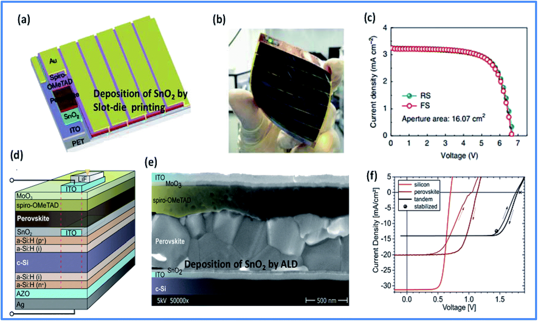 | ||
| Fig. 19 (a) Structure of the 6 sections of series-connected large-area flexible PSCMs. (b) Photograph of the flexible PSCM and (c) the corresponding J–V curves of the champion flexible PSCM.253 (d) Schematic device design of the silicon heterojunction/perovskite tandem solar cell. The red dashed line indicates the active area. (e) Cross-sectional scanning electron micrograph of a typical monolithic tandem solar cell. (f) J–V characteristics of tandem, perovskite standalone and Si standalone cells,254 presented with permission and copyright. | ||
SnO2 was also found to be very effective as an electron selective contact in the case of 2-terminal monolithic tandem solar cells. A low temperature processed electron selective layer is highly commended since the bottom cell of the tandem structure could be damaged by the high-temperature process. Albrecht et al.254 reported a 2-terminal monolithic tandem solar cell using Si as the bottom cell, PSCs as the top cell and ALD-grown SnO2 as the electron selective contact and achieved an efficiency of 19.9% with a VOC of 1785 mV (Fig. 19d–f).
Liang et al. investigated a new arrangement of OMO structure, tungsten oxide, and WO3 (23 nm)/Ag (10.7 nm)/SnO2 (35 nm) with the lowest sheet resistance and high visible transmittance.255 The device conversion efficiency boosted to 14% with a high JSC (7.9 mA cm−2 to 18.6 mA cm−2) and a high FF from 0.24 to 0.72 due to the SnO2 NP interfacial layer.255 This work suggested a big potential of OMO in the replacement of ITO in flexible solar cell applications. Similarly, Hashemi et al. reported different approaches to develop flexible and wearable solar cells for self-powered wearable devices.256Table 5 compares the device performances of perovskite based solar cells for doped SnO2.
| Method | Device layer (SnO2) | Doping/foreign element(s) (SnO2) | V OC (V) | J SC (mA cm−2) | FF (%) | PCE (%) | Reference |
|---|---|---|---|---|---|---|---|
| a Abbreviations: ITO = indium tin oxide, FTO = fluorine doped tin oxide, ZTO = zinc tin oxide, CNT = carbon nanotube, QD = quantum dot, HT SnO2 = high temperature tin oxide, LT SnO2 = low temperature tin oxide, PEN-Br = poly(9,9-bis(3′(N,N-dimethyl)-N-ethylammonium-propyl-2,7-fluorene)-alt-2,7-(9,9-dioctylfluorene))dibromide, spiro-OMeTAD = 2,2′,7,7′-tetrakis[N,N-di(4-methoxyphenyl)amino]-9,9′-spirobifluorene, PET = polyethylene terephthalate, SnO2 ESL = tin oxide electron selective layer, HTM = high temperature mesoporous, FAPbI3 = single crystal formamidinium lead iodide, MAPbI3 (or) MAPI = methylammonium lead halide, PCBM = phenyl C-61 butyric acid methyl ester, NPT = nitrogen plasma treated, HTL = hole transporting layer. | |||||||
| Sol–gel | FTO/SnO2 (Zr/F)/CH3NH3PbI3/SiGe/spiro-OMeTAD/Au | Zr/F | 1.105 | 24.39 | 71.2 | 19.19 | Tian et al.257 |
| Solvothermal | SnO2–TiO2 | TiO2 | 0.76 | 7.18 | 60.41 | 3.28 | Qureshi et al.258 |
| Spinning | FTO/Cu–SnO2/CH3NH3PbI3/spiro-OMeTAD/Au | Cu | 0.78 | 21.74 | 0.509 | 8.48 | Li et al.259 |
| Spinning | FTO/Zn–SnO2/CH3NH3PbI3/spiro-OMeTAD/Au | Zn | 0.97 | 22.24 | 0.610 | 13.17 | Li et al.259 |
| Spinning | FTO/Cd–SnO2/CH3NH3PbI3/spiro-OMeTAD/Au | Cd | 0.90 | 20.56 | 0.487 | 9.03 | Li et al.259 |
| Spinning | FTO/Li–SnO2/CH3NH3PbI3/spiro-OMeTAD/Au | Li | 0.46 | 18.99 | 0.423 | 3.76 | Li et al.259 |
| Spinning | FTO/Ti–SnO2/CH3NH3PbI3/spiro-OMeTAD/Au | Ti | 1010 | 21.49 | 66.6 | 14.45 | Li et al.259 |
| Doctor blade technique | SnO2–ZnO | ZnO | 6.38 | 0.60 | 0.46 | 1.75 | Sujinnapram et al.260 |
| Sol–gel | ITO/Li: SnO2 | ITO/Li | 1.10 | 23.27 | 70.71 | 18.20 | Park et al.241 |
| Sol–gel | SnO2/NH4Cl–SnO2 | NH4Cl | 1.10 | 24.37 | 78.31 | 21.01 | Song et al.261 |
| Sol–gel | SnO2-CNT | CNT | 1.12 | 23.26 | 78.23 | 20.33 | Tang et al.262 |
| Magnetron sputtering | FTO/SnO2 (Ar:O2) | FTO | 1.05 | 22.45 | 0.76 | 18.20 | Bai et al.263 |
| Spin-coating | SnO2/PFN-Br | PFN-Br | 1.09 | 23.46 | 77.2 | 19.77 | Guo et al.264 |
| Sol–gel | SnO2/CH3NH3PbI3/SiGe/spiro-OMeTAD/SiGeSn | CH3NH3PbI3/SiGe/spiro-OMeTAD/SiGeSn | 0.78 | 49.75 | 73.4 | 28.57 | Kumar et al.265 |
| Spin-coating | ITO/SnO2/CH3NH3PbI3/SiGe/spiro-OMeTAD/Ag | CH3NH3PbI3/SiGe/spiro-OMeTAD/Ag | 1.08 | 19.5 | 0.62 | 13 | Song et al.266 |
| Sol–gel | FTO/SnO2/CH3NH3PbI3/SiGe/spiro-OMeTAD/Au | CH3NH3PbI3/SiGe/spiro-OMeTAD/Au | 1.11 | 23.27 | 0.67 | 17.21 | Ke et al.236 |
| Sol–gel | ITO/SnO2/CH3NH3PbI3/SiGe/spiro-OMeTAD/Au | CH3NH3PbI3/SiGe/spiro-OMeTAD/Au | 1.084 | 21.98 | 64.17 | 15.29 | Park et al.241 |
| Sol–gel | PFT/ITO/SnO2/meso-TiO2 | Meso-TiO2 | 20.70 | 1.036 | 65.55 | 14.07 | Dagar et al.267 |
| Sol–gel | FTO/SnO2ESL/CH3NH3PbI3/spiro-OMeTAD/Au | CH3NH3PbI3/spiro-OMeTAD/Au | 1.09 | 18.48 | 75.04 | 15.10 | Ke et al.268 |
| Sol–gel | Glass/FTO/SnO2/CH3NH3PbI3/spiro/Au (UVLT-SnO2) | CH3NH3PbI3/spiro/Au (UVLT-SnO2) | 1.06 | 21.94 | 61.73 | 14.36 | Huang et al.269 |
| Sol–gel | Glass/FTO/SnO2/CH3NH3PbI3/spiro/Au (HT-SnO2) | CH3NH3PbI3/spiro/Au (HT-SnO2) | 1.06 | 19.82 | 57.40 | 11.49 | Huang et al.269 |
| Spin-coating | FTO/SnO2/CH3NH3PbI3/CuSCN/Au (water) | CH3NH3PbI3/CuSCN/Au (water) | 0.95 | 18.19 | 0.38 | 6.59 | Murugadoss et al.270 |
| Spin-coating | FTO/SnO2/CH3NH3PbI3/CuSCN/Au (ethanol) | CH3NH3PbI3/CuSCN/Au (ethanol) | 0.96 | 18.99 | 45 | 8.38 | Murugadoss et al.270 |
| Sol–gel | FTO/SnO2/CH3NH3PbI3/spiro-OMeTAD/G | CH3NH3PbI3/spiro-OMeTAD/G | 1.05 | 22.78 | 78 | 18.65 | Zhang et al.271 |
| Sol–gel | FTO/CL/SnO2/TiO2/CH3NH3PbI3/HTM/Au | TiO2/CH3NH3PbI3/HTM/Au | 0.99 | 20.70 | 59.9 | 12.23 | Duan et al.272 |
| Sol–gel | FTO/SnO2/CH3NH3PbI3/SiGe/spiro-OMeTAD | CH3NH3PbI3/SiGe/spiro-OMeTAD | 1.05 | 22.8 | 66.2 | 15.8 | Pinpithak et al.273 |
| Sol–gel | FTO/SnO2ESL/CH3NH3PbI3/meso/HTM/Ag | CH3NH3PbI3/meso/HTM/Ag | 0.95 | 18.92 | 0.70 | 12.67 | Dong et al.274 |
| Sol–gel | ITO/SnO2/(FAPbI3)0.97–(MAPbBr3)0.03/spiro/Au | (FAPbI3)0.97–(MAPbBr3)0.03/spiro/Au | 1.13 | 23.69 | 80.61 | 21.52 | Jiang et al.275 |
| Sol–gel | FTO/SnO2/(FAPbI3)0.875–(CsPbBr3)0.125/spiro/Au | (FAPbI3)0.875–(CsPbBr3)0.125/spiro/Au | 1.07 | 21.26 | 0.74 | 16.80 | Jung et al.243 |
| Sol–gel | FTO/SnO2 QD/CH3NH3PbI3/spiro-OMeTAD/Au | QD/CH3NH3PbI3/spiro-OMeTAD/Au | 1.11 | 20.94 | 0.73 | 16.97 | Yang et al.276 |
| Spin-coating | FTO/bl/meso-SnO2/CH3NH3PbI3/spiro/Au | CH3NH3PbI3/spiro/Au | 1.11 | 22.80 | 75.78 | 19.21 | Xiong et al.277 |
| Spin-coating | FTO/m-SnO2/CH3NH3PbI3/spiro-OMeTAD/Au | CH3NH3PbI3/spiro-OMeTAD/Au | 983 | 21.1 | 63 | 13.1 | Roose et al.278 |
| Hydrothermal | FTO/SnO2 nanosheet CH3NH3PbI3/spiro-/Au | CH3NH3PbI3/spiro-/Au | 1.05 | 22.76 | 0.68 | 16.17 | Liu et al.279 |
| Sol–gel | FTO/Nb:SnO2/CH3NH3PbI3/spiro-/Au | CH3NH3PbI3/spiro-/Au | 1.08 | 22.36 | 0.72 | 17.57 | Ren et al.280 |
| Hydrothermal | FTO/SnO2 nanosheet/C60/CH3NH3PbI3/spiro-/Au | C60/CH3NH3PbI3/spiro-/Au | 1.03 | 23.62 | 75 | 18.31 | Wu et al.281 |
| Atomic layer deposition | FTO/SnO2/CH3NH3PbI3/HTL/Au | CH3NH3PbI3/HTL/Au | 1.14 | 21.3 | 74 | 18.4 | Baena et al.234 |
| Pulse layer deposition | FTO/SnO2/PCBM/CH3NH3PbI3/spiro-/Au | PCBM/CH3NH3PbI3/spiro-/Au | 1.11 | 21.6 | 71 | 17.03 | Chen et al.282 |
| Chemical bath deposition | FTO/SnO2/CH3NH3PbI3/spiro-OMeTAD/Au | CH3NH3PbI3/spiro-OMeTAD/Au | 1.13 | 22.95 | 79 | 20.56 | Bu et al.283 |
| Hydrothermal | HT/FTO-SnO2 | HT/FTO | 1.08 | 21.35 | 74.89 | 17.37 | Liu et al.252 |
| Spin-coating | ITO/SnO2/ZTO/CH3NH3PbI3/spiro-OMeTAD/Au | ZTO/CH3NH3PbI3/spiro-OMeTAD/Au | 1.13 | 22.6 | 80.2 | 20.5 | Guo et al.284 |
| Spin-coating | FTO/SnO2/MAPbI3/spiro-OMeTAD/Au | MAPbI3/spiro-OMeTAD/Au | 1.11 | 21.44 | 74.58 | 17.83 | Zhang et al.285 |
| Sol–gel | NPT-SnO2 | NPT | 1.12 | 21.82 | 0.83 | 20.3 | Subbiah et al.286 |
| Sputtering | FTO/SnO2/CH3NH3PbI3/spiro-OMeTAD/Au | CH3NH3PbI3/spiro-OMeTAD/Au | 1.08 | 23.7 | 0.79 | 20.3 | Qiu et al.287 |
| Plasma treatment | FTO/c-SnO2/MAPI/CH3NH3PbI3/spiro-OMeTAD/Au | MAPI/CH3NH3PbI3/spiro-OMeTAD/Au | 108 | 20.4 | 76.3 | 19.4 | Méndez et al.288 |
6.3 Plasma treated SnO2 for PSCs
Over the past few decades, plasma processing has become a tool for various manufacturing and materials processing industries. Plasma technologies have found applications in aerospace, automotive, steel, biomedical, and toxic waste management industries.289 Most importantly, plasma processing is now well adopted in large scale integrated circuit manufacturing. The primary properties of plasmas that have attracted the attention of industries include high power and energy density of thermal plasmas used in additive manufacturing and the abundant presence of reactive species capable of initiating chemical reactions on their own.290 These reactive species can perform complex transformations that are in many ways beyond the scope of other conventional techniques. One of the major advantages of using plasma technologies, in particular, for oxide semiconductors is that these processes are dry and environmentally friendly. In this sub-section, we emphasize on non-thermal plasma induced processing of SnO2 nanostructures. Non-thermal plasmas are advantageous as they can be operated at low temperatures and provide unique opportunities for low-temperature material processing.Plasma-based processes are indispensable in reactive sputtering and plasma-enhanced CVD. These techniques are widely used for the synthesis of high-quality SnO2 nanostructures that are used for a varied range of applications.291–293 In this context, Tarlov and Evans were among the first to study the effect of plasma functionalization on SnO2 thin films.294 They demonstrated that RF water plasma treatment of SnO2 films is an excellent method for preparing “clean”, hydroxylated surfaces. They studied the hydroxylated surfaces using angle-resolved X-ray photoelectron spectroscopy and electron energy loss spectroscopy, to identify the changes in surface electronic states and chemical properties. Interestingly, the plasma treatment removed the oxygen vacancies by restoring the Sn4+ valency in the surface region. In general, plasma treatment also removed unwanted carbon contaminants with no preferential surface hydroxylation. This study reintroduced plasma-based systems as a new synthesizing route for oxides in general and in particular to SnO2 surfaces. Since then, there have been a plethora of reports on plasma engineered SnO2 nanostructures for a wide range of applications, e.g. photovoltaics, sensors and catalysis.57,85,295
SnO2 thin films are typically used as a TCO for the front electrode in silicon thin-film solar cells, due to their wide bandgap (∼3.6 eV), transparency in the visible region and high electrical conductivity. Hydrogen plasma is commonly used to prepare hydrogenated amorphous and microcrystalline silicon films.296 Towards this end, Kim et al. studied the effects of hydrogen plasma treatment on the structural and electrical properties of sputtered SnO2 thin films.186 They found that hydrogen plasma treatment degraded the crystalline quality and optical transmittance and cause etching of the SnO2 films. Interestingly, hydrogen plasma treatment led to improved electrical conductivity along with the increase in carrier concentration, and this was attributed to the formation of oxygen vacancies in undoped SnO2 films. Tang et al. were able to modulate the electronic properties, surface energy, and roughness of fluorine-doped SnO2 films using oxygen plasma treatment.297 Both the work function and hydrophilicity of SnO2 were found to increase after oxygen plasma treatment. In a unique approach, Chen and Thimsen were able to synthesize highly conductive ATO nanocrystals using dual-nonthermal plasmas.112 They were able to achieve a high conductivity of 0.1 S cm−1 for the as-deposited porous ATO films prepared using this approach. During the synthesis, Sn and Sb vapor precursors were fed into a dual-zone (discharge) flow-through plasma reactor. The reagent passed through the first plasma zone to form metallic Sb–Sn alloy NPs. From the first discharge (zone 1), the alloy NPs followed the carrier gas through to the second discharge (zone 2) containing O2 to become oxidized. The ATO nanocrystals were then deposited onto various substrates (silicon wafer, glass, fused silica, or single crystal NaCl). The as-deposited films showed a high optical transmittance of >90% over the entire visible wavelength regime. Hence, ex situ plasma treatment could be used to modify the surface composition, energy band structure, and surface energy to facilitate efficient carrier transport at the FTO interfaces, eventually improving the device performance.
Like silicon solar cells, SnO2 plays a critical role in PSCs as well.298 The high dopant concentration (Nd = 1020 cm−3) in FTO results in the formation of a very thin space charge region at the interface. The decrease in the width of the space charge region increases the probability of electrons tunneling across, resulting in a reduced performance. To overcome this issue, it is customary to introduce a thin layer of the electron blocking layer (metal oxide) in the form of TiO2 or SnO2 atop FTO. However, the growth or deposition of this electron blocking layer faces several challenges such as the formation of pinholes and uniform thickness. To overcome this, Dao et al. developed a new strategy to increase the uniformity and reduce the pinholes in the TiO2 layer by atmospheric pressure plasma treatment of FTO.299 They observed a significant increase in the efficiency of the PSC where the TiO2 blocking layer was deposited on plasma-treated FTO. Argon plasma (150 W) treatment for 1 minute transformed the FTO surface superhydrophilic. The increase in the efficiency was attributed to the suppression of electron recombination at the FTO interfaces due to the high-density, uniform, and pinhole-free TiO2 layer on the surface of the plasma-treated FTO.
In another interesting work, Wang et al. demonstrated that a low temperature processed SnO2 could be an excellent material for the electron selective layer (ESL) material.300 Through plasma-enhanced atomic layer deposition (PEALD) they could deposit SnO2 at temperatures less than 100 °C, which is significant, considering the compatibility with large-scale roll-to-roll manufacturing and other potential opportunities for flexible solar cells. The as-fabricated PSCs with SnO2 deposited through PEALD and passivated with a C60-self-assembled monolayer exhibited maximum PCEs of 19.03% and 16.80% under reverse voltage on glass and flexible polymer substrates, respectively, as shown in Fig. 20. In the same way, Kuang et al. also used PEALD for SnO2 in PSCs.301 They studied the influence of deposition temperature on the material properties of SnO2. Highly transparent amorphous SnO2 films were prepared in a temperature range of 50–200 °C. The film deposited at 200 °C showed the best band alignment at the SnO2:perovskite interface, while the film deposited at 50 °C showed a considerable band offset. However, for a 15 nm thick layer, this band offset did not affect the electron transport at the interface and the PSCs with either 50 or 200 °C SnO2 ETL demonstrated comparable initial PCEs. The SnO2 films fabricated at 50 °C were found to be resistive, while the 200 °C SnO2 films showed a low electrical resistivity of 1.8 × 10⁻³ Ω cm and high carrier density and mobility of 9.6 × 1019 cm−3 and 36.0 cm2 V−1 s−1, respectively. As a result, the PSCs with 200 °C SnO2 retain their initial performance at the maximum power point for over 16 h. Thus, the reports by Wang et al. and Kuang et al. envisage the prospect of integrating PEALD for roll-to-roll applications.300,301
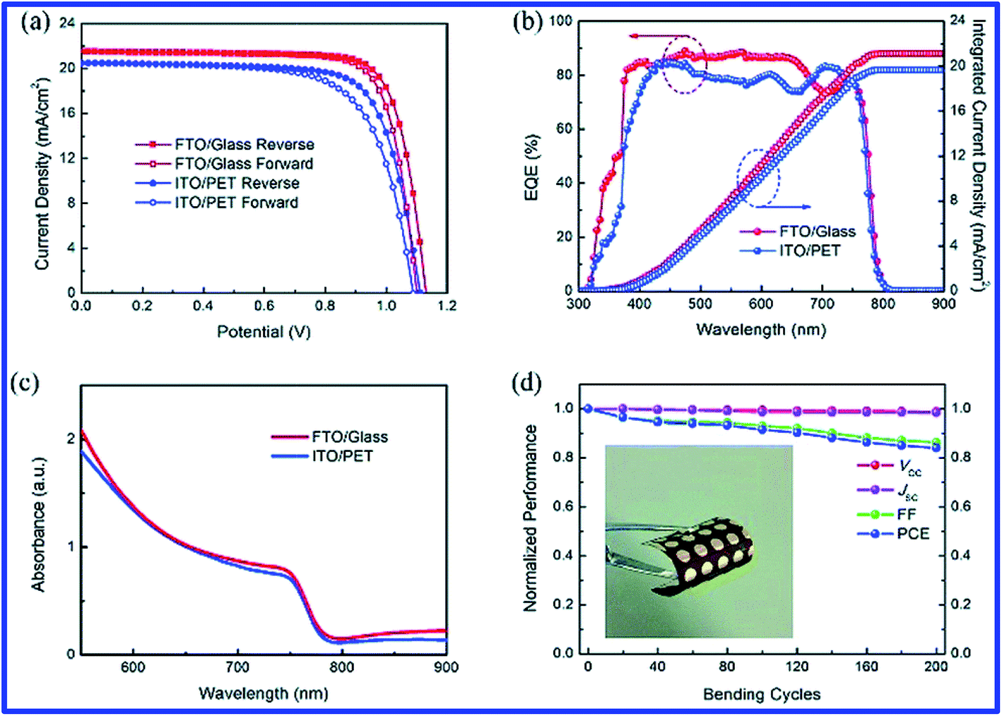 | ||
| Fig. 20 The best-performing devices based on PEALD SnO2 coated FTO/glass and ITO/PET substrates: (a) J–V curves under reverse and forward voltage scans. (b) EQE spectra and their corresponding integrated photocurrents. (c) Absorption spectra of perovskite films. (d) Normalized performance parameters of a flexible PVSC versus bending cycles. Photograph of a flexible device after the bending test (inset),300 presented with permission and copyright. | ||
Hu et al. used SnOx grown by ALD as an electron extraction layer to design ITO-free PSCs.302 They replaced ITO with a semitransparent SnOx/Ag electrode, which simultaneously served as an electron extraction layer delivering a PCE of 11%. They thoroughly investigated the electronic properties of SnOx grown by ALD using H2O, ozone, or oxygen plasma as the oxidant. Though there were no obvious differences in the crystal structure, morphology, or surface energy between the SnOx samples, the PSCs showed different performances. However, work function measurements using Kelvin probe microscopy and ultraviolet photoelectron spectroscopy (UPS) on these SnOx layers showed a trend of plasma–SnOx > H2O–SnOx > ozone–SnOx. Interestingly, only for H2O–SnOx, an oxygen vacancy induced gap state (GS) at about 2.23 eV below the Fermi level was observed only for H2O–SnOx. They also found that there is always formation of the PbI2 interfacial layer with an electronic bandgap of 2.19 eV between MAPbI3 and SnOx. Fig. 21 shows the interfacial electronic band alignment for three SnOx electrodes. Based on their measurements and performance, they concluded that ozone–SnOx was the best hole blocking layer and designed an ITO-free semitransparent bottom electrode based on SnOx/Ag/SnOx architecture. Here, H2O–SnOx acted as the permeation barrier to protect the Ag from corrosion.
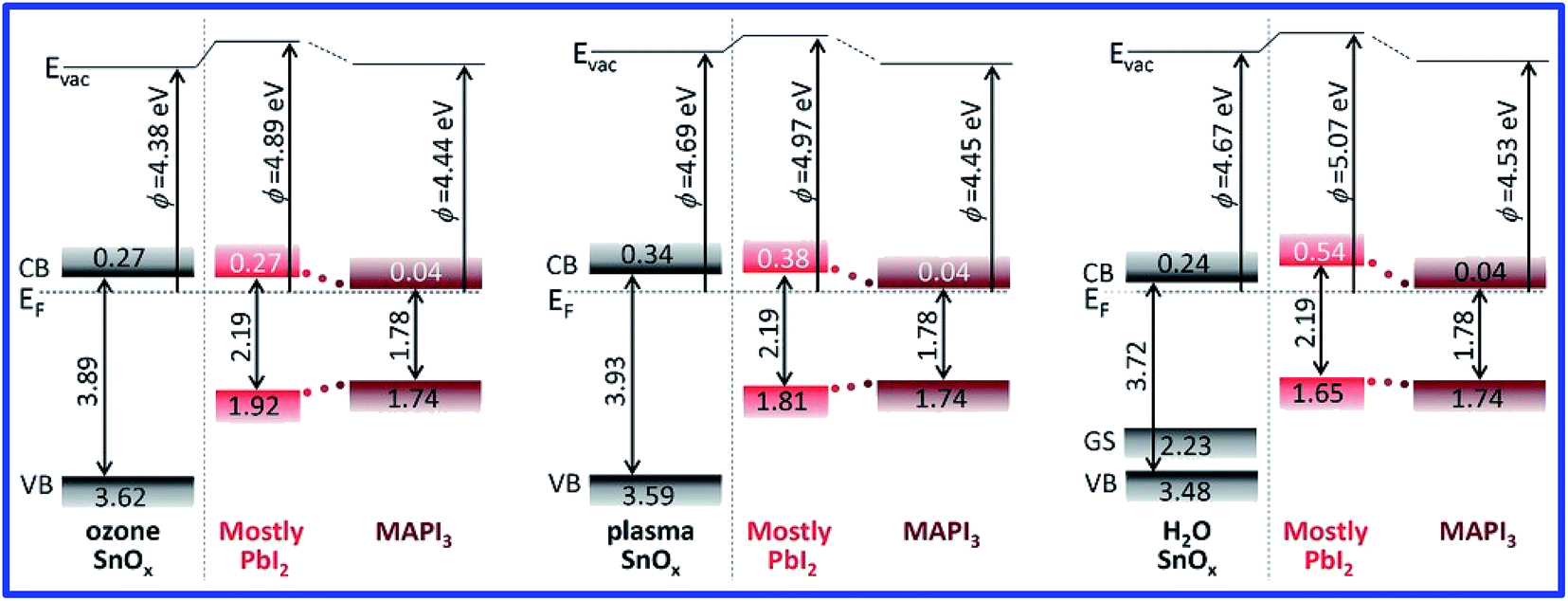 | ||
| Fig. 21 Electronic structure of different SnOx variants in their pristine state and of a thin and thick (bulk-like) MAPbI3 layer deposited on top of them. The energy level positions were determined by UPS and IPES measurements. Abbreviations—Evac: vacuum level; EF: Fermi energy; and φ: work function. The values written at the VB and the CB mark their distance from the Fermi energy,302 presented with permission and copyright. | ||
Although ALD and sputtering techniques can produce uniform and crystalline thin films, their integration onto large scale production and roll-to-roll fabrication routes is a challenge. From a practical point of view, it is important to simplify the entire fabrication process to address these challenges. For this purpose, Yu et al.303 devised a superfast (<5 min) facile route to synthesize SnO2 at room-temperature (<50 °C) using atmospheric Ar/O2 plasma, as shown in Fig. 22a. Compared with thermally annealed SnO2 (T-SnO2) thin films, the plasma synthesized SnO2 films exhibited superior properties viz. higher electrical conductivity, better electron mobility, and low density of charge trap sites. Consequently, plasma synthesized SnO2 based PSCs achieved a superior PCE of 19.56%. The comparatively high PCE was attributed to efficient electron extraction and reduced nonradiative recombination at the plasma synthesized-SnO2 ETL/perovskite interface, which relaxed the hysteresis and improved the resistance of PSCs to sunlight.
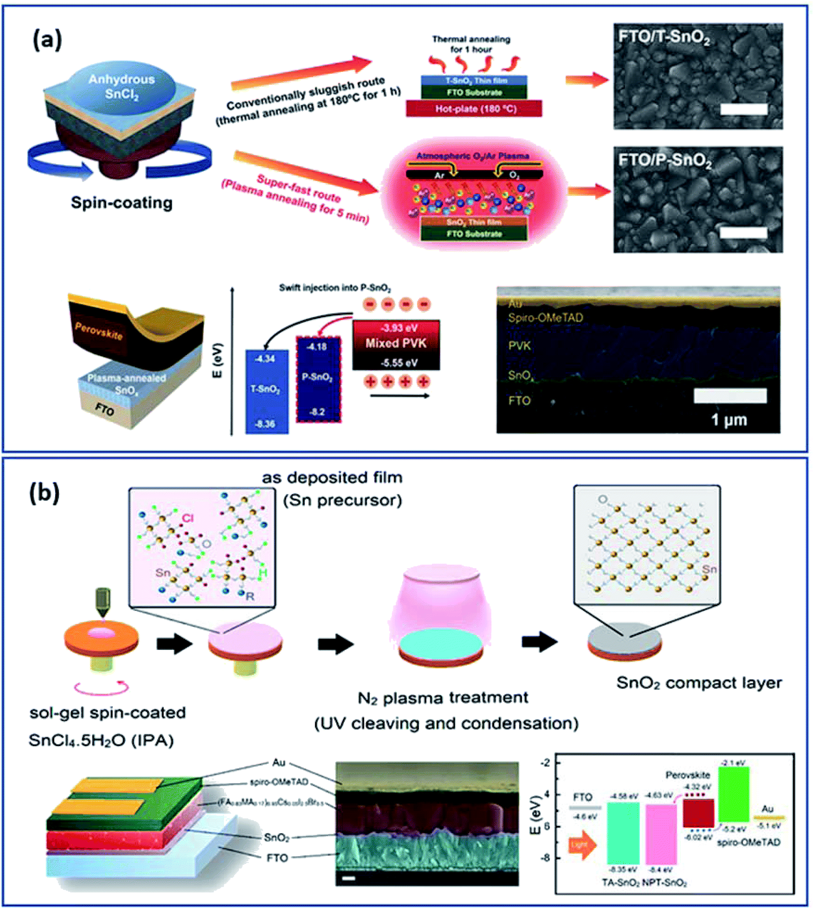 | ||
| Fig. 22 Schematic of SnO2 thin film fabrication by (a) Yu et al. using thermal or O2/Ar plasma with corresponding field-emission scanning electron microscopy (FE-SEM) images. T-SnO2 was annealed at 180 °C for 60 min, and P-SnO2 was developed by plasma energy with gas flow rates of 0.008 L h−1 (Ar) and 0.06 L h−1 (O2) for 5 min.303 (b) Subbiah et al. using a modified sol–gel technique by employing low-power RF N2 plasma exposure for 60 min in an approximate pressure of 1 Torr,286 presented with permission and copyright. | ||
Another approach to improve the efficiency of solution-processed PSCs was proposed by Subbiah et al.286 This involved the use of a low-power N2 plasma to form compact SnO2 from a spin-coated SnCl4·5H2O solution, as schematically shown in Fig. 22b. Most importantly, this technique could be applied to fabricate PSCs on rigid as well as on flexible substrates. When compared with O2 plasma treatment, SnO2 film formation from the Sn metal halide precursor materialized only in the presence of a N2 plasma. This was attributed to the deep UV emission lines (ca. 290–390 nm) of N2 plasma alongside the NO* species, which provide the necessary energy to initiate the cleaving of metal alkoxy bonds. To prove the effectiveness of the process, they compared the PSC performance composed of either N2 plasma-treated (NPT-SnO2) or thermally oxidized (TA-SnO2) films. The champion device with NPT-SnO2 as the ETL witnessed a PCE of 20.3%, a VOC of ∼1.12 V, an FF of ∼0.83, and a JSC of ∼21.82 mA cm−2 under the reverse scan, whereas the TA-SnO2-based champion device demonstrated a PCE of 19.9%, a VOC of ∼1.08 V, an FF of ∼0.81, and a JSC of ∼22.9 mA cm−2. The flexible device fabricated with NPT-SnO2 showed a best PCE of 18.1% under a reverse scan, with the corresponding performance parameters of VOC ∼ 1.05 V, FF ∼ 0.76, JSC ∼ 22.8 mA cm−2 and a stable PCE of 17.1%. It is to be noted that a layer of mesoporous alumina (Al2O3) was introduced on top of NPT-SnO2 to compensate for the presence of pinholes. Importantly, the device retained 90% of the initial PCE after 1000 cycles of bending. Details related to the flexible device are presented in Fig. 23.
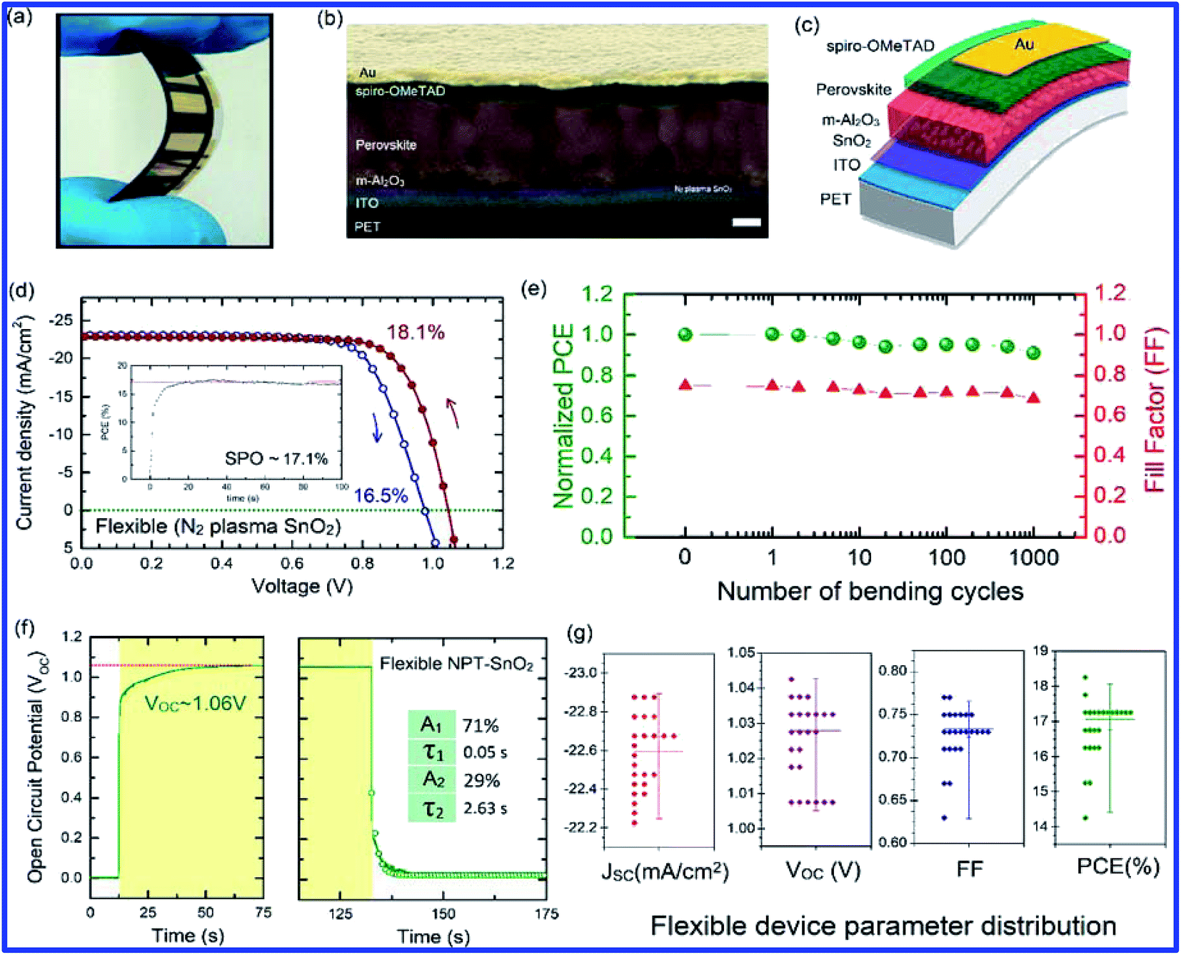 | ||
| Fig. 23 (a) Photograph depicting the flexible nature of the devices fabricated using room-temperature NPT-SnO2 ETL. (b) SEM cross-sectional image of a flexible device. (c) Device architecture schematic of the flexible device fabricated by Subbiah et al.286 (d) Champion light J–V characteristics of the flexible device with a PCE of 18.1% and a stable power output efficiency of 17.1% under 1 sun illumination. (e) Normalized device efficiency and fill factor of the flexible device being subjected to 1000 bending cycles. (f) Transient VOC measurements in the seconds scale to illustrate the associated rise and decay constants. (g) Histogram of the various device parameters extracted from a batch of 24 flexible devices. All efficiencies were measured under the reverse scan,286 presented with permission and copyright. | ||
Recently, Smith et al. studied the post-processing effects of spray-coated SnO2 films by UV ozone or O2 plasma on the device performance.304 The device with UV ozone treated ETL outperformed the one with the O2 plasma-treated ETL. The O2 plasma apparently makes the surface Sn-rich and O-poor. It was also found that plasma treatment significantly downshifted the Fermi level, resulting in a loss of electron selectivity along with a drop in VOC and an increase in J–V hysteresis. Hence, in some cases, O2 plasma can have a detrimental impact on the SnO2/perovskite interface and device performance. To gain a better understanding, Luan et al. were able to increase the PCE by employing O2 plasma treatment to treat 2,2,2-trifluoroethanol (TFE)-incorporated SnO2 ETL films.244 The presence of a strong electron-withdrawing group (trifluoromethyl) improved the electron mobility in the SnO2 ETL. They found that by carefully controlling the plasma power to 60 W used for treating SnO2, the PCE could be increased from 20.92% to 21.68% (VOC: 1.12 V, JSC: 24.06 mA cm−2 and FF: 0.802). However, at higher power (140 W), VOC dropped from 1.12 V to 1.07 V due to the increase in the work function (from 4.21 to 4.40 eV) away from the conduction band of the perovskite film (4.18 eV) similar to the findings of Smith et al.304
A significant amount of research has been conducted on graphenes during the last decade. This is driven by the realization of the immense capabilities possessed by this wonder material. Applications are already recognized in a wide range of disciplines from ultra-fast and flexible electronics to optoelectronic devices, supercapacitors, water remediation, DNA attachment, photocatalysis, oxygen reduction reaction catalysts, and many more. To realize these pathways, functionalization of graphene and its oxide played a crucial role. Many techniques of functionalization have been applied to extend the application prospects of graphene.142
In the present review, we discuss the plasma engineering of oxide surfaces as a potential alternative to conventional techniques. Plasma functionalization is advantageous in terms of controllability and selectivity associated with it. The ionic species present in plasma can tune the electronic and optical properties of oxides and can even control the surface energy and processes. Wet chemical functionalization involving precursors and by-products fails in achieving localized effects in oxide semiconductors for PV applications. With plasma functionalization, it is possible to precisely tailor-design oxide properties by inducing localized charges. The advantages of this technique include time and cost-effectiveness. This process is environmentally friendly and opens up future pathways for large-scale industrial implementation. However, most of the plasma processes involve low-pressure vacuum-based systems. Atmospheric pressure plasma can be a promising candidate for various plasma-based functionalization applications. In atmospheric pressure plasma jet (APJJ), the plasma is not confined within the dimensions of the electrodes. Nevertheless, it is important to understand the characteristics of plasma being used, to make the process beneficial.
6.4 Thermally treated SnO2 for PSCs
For SnO2 thin films, the effect of the annealing temperature on the film properties is a key parameter as it has influence on its electrical properties (resistivity, carrier concentration and mobility, and conductive type), surface morphology, and crystal quality of the films. Optimization of parameters is essential to fabricate efficient devices. Normally, SnO2 films treated at higher temperatures will exhibit better crystallinity, which improves the charge carrier and the optical transmittance.57,305 Yuan et al. demonstrated the influence of the thermal annealing temperature on the electrical and optical properties of SnO2 thin films deposited on glass substrates by spin-coating.306 SnO2 films annealed in air show an increase in the optical transmittance by increasing the annealing temperature from 100 to 300 °C, but the transmittance decreased upon further increasing the temperature to 500 °C. Particles in the film annealed at 100 °C show a high surface roughness. When the temperature was increased to 300 °C, the surface roughness of the films decreased due to the increase in the surface diffusion of atoms with higher kinetic energy. At 500 °C, cracks and blisters occurred due to the rapid growth of the particles, resulting in an increase in surface roughness. As a result, the transmittance of SnO2 thin films decreased at 500 °C. An annealing temperature below 500 °C has a positive effect on the sheet resistance and transmittance in the visible light region of SnO2 thin films.Generally, for the fabrication of high-efficiency solar cells, metal-oxide electron selective layers (ESLs) annealed at high temperatures (HT) are preferred over those at low-temperatures (LT), due to the higher carrier mobility.57 However, as demonstrated by Ke et al., for the SnO2 ESLs, the situation is quite different.268 To compare the efficiency of low- and high-temperature annealed SnO2 on the performance of perovskite solar cells (PSCs), the authors prepared SnO2 films over FTO substrates by spin coating of the SnCl2·2H2O precursor, followed by thermal annealing in air at 185 °C (LT-SnO2) and at 500 °C (HT-SnO2) for 1 h. Perovskite solar cells using LT-SnO2 ESLs exhibited a better performance than the cells using HT-SnO2, due to a better film coverage, lower electron concentration, higher electron mobility, and a wider band gap. The use of LT annealing of SnO2 ESL is an important advantage due to its low cost, easy preparation, and better performance in PSCs.
Another way to improve the photovoltaic performance by boosting the electrical conductivity of SnO2 ESLs is using thermal annealing to reduce or even eliminate the current density–voltage (J–V) hysteresis. Jung et al. used tin(IV) isopropoxide as the precursor to deposit SnO2 ETL films onto the FTO glass substrate.243 The films were annealed in ambient air at 100, 150, 200, 250, 300, 350, 400 and 500 °C for 30 min. The results showed that the J–V curves and the photovoltaic performance depend on the annealing temperature. The difference between the reverse and forward scanned J–V curves decreased as the temperature was increased from 150 °C to 250 °C, which minimized at 250 °C and then increased again as the temperature was increased from 300 °C to 500 °C. This behaviour directly affected the power conversion efficiency (PCE), which reached a maximum average value of 16.08% at 250 °C. Similar results were also reported by Wang et al.307 The photovoltaic performance of PEALD SnO2 ESLs was improved by low-temperature thermal annealing in ambient air due to a reduction in the imbalance of charge transportation and consequently to a significant reduction in the degrees of J–V hysteresis.
The change in the annealing temperature is also capable of modifying the conducting type of transparent conductive SnO2:Zn thin films, as shown in Ni et al.201 Based on the Hall measurements, it can be confirmed that the SnO2:Zn films annealed below 400 °C possessed an n-type behaviour. Upon increasing the annealing temperature within the range of 400–500 °C, the films showed a p-type conductivity, but at 500 °C an increase in resistivity and a decrease in carrier concentration were also observed. Finally, for the films annealed above 500 °C, a conversion in conductivity from p-type only to both p-type and n-type as the major and secondary conduction type occurred. This behaviour might be attributed to the inability of Zn atoms to substitute Sn at lower temperatures due to a lack of activation energy. When the annealing temperature increases, the acceptor effect of Zn substituting Sn is activated, resulting in p-type films.
Several studies indicate that a strong correlation exists between the characteristics of the SnO2 layer and the device performance, which is strictly connected to surface chemistry. For example, Wang et al.308 demonstrated a mesoporous SnO2 (m-SnO2) layer with different concentrations of polyethylene glycol (PEG) (0, 3, 6, 9, and 12%). The colloidal SnO2 precursor solution was spin coated (4000 rpm, 20 s) on the ITO substrate with and without PEG and then annealed at 180 °C for 20 min. The device exhibits excellent performance with a PCE of 20.82%, a VOC of 1.10 V, a JSC of 24.56 mA cm−2, and an FF of 77.10%.308 Kuang et al. fabricated a SnO2 based device (glass/ITO/ALD SnO2/CH3NH3PbI3/spiro-OMeTAD/Au) with different annealing temperatures. The solar cell exhibited a PCE of 16.2%, a VOC of 1.086 V, a JSC of 21.4 mA cm−2, and an FF of 70% for the SnO2 film annealed at 50 °C and a PCE of 16.1%, a VOC of 1.061 V, a JSC of 21.3 mA cm−2, and an FF of 71% for the SnO2 film annealed at 200 °C (Fig. 24).301 The improvement of device performance after thermal treatment at 50 °C is due to the presence of a conduction band offset of ∼0.69 eV at the SnO2/perovskite interface. On the other hand, there is a negligible conduction band offset found after thermal treatment at 200 °C. It is also worth noting that the stability of the device significantly depends on the thermal treatment. PSCs retain their initial performance over 16 h under continuous one sun illumination in an inert atmosphere for the SnO2 treated at 200 °C, whereas the PCE decreases by ∼50% for the device with SnO2 treated at 50 °C.
 | ||
| Fig. 24 (a) Schematic representation of plasma-assisted atomic layer deposition of the SnO2 layer (glass/ITO/ALD SnO2/CH3NH3PbI3/spiro-OMeTAD/Au) with its PCE performance; (b) XRD analysis of SnO2 at different annealing temperatures; and (c) steady state and time resolved photoluminescence of SnO2, presented with permission and copyright.301 | ||
7. SnO2 for the sustainable building technology
7.1 Transparent/semi-transparent BIPV devices
An emerging application of transparent conducting SnO2 films is in the field of transparent photovoltaics (TPV).309 Unlike the conventional thin-film solar cells which are typically opaque devices with a dark-colored absorber and one reflective cathode, the TPV devices consist of a transparent cathode and a light-transmitting absorber on a transparent substrate. This new category of solar cells has generated a great deal of research interest in the past several years being partially or fully transmitting to visible sunlight. The TPV devices can be integrated into smart windows or energy harvesting facades during the construction of energy-efficient (green) buildings.310 These building integrated photovoltaic (BIPV) devices offset the electricity consumed by various building services and reduce the overall carbon footprint of the building. Carbon mitigation is expected to be substantial because a high percentage of electricity generated in a developed economy is used in buildings. BIPV provides an important complement to the decentralized generation of electricity from building applied photovoltaics (BAPV) such as retrofitted roof top solar modules by making use of the large amount of vertical or slanted surfaces on the exterior of multi-storey buildings. TPV equipped windows can limit the amount of heat entering the interior of a building. In addition, for fully transparent TPV devices, the incorporation of these devices will not only adversely alter the aesthetic appeal of the architecture but also can be readily adopted in energy-efficient buildings.Before reviewing the recent developments in TPV devices fabricated based on SnO2 coated substrates, it is important to mention the key device characteristics of TPV devices, namely (1) visible light-transmitting property and (2) power conversion efficiency (PCE), which is a necessary but not sufficient parameter for describing the TPV device performance. Two additional parameters, namely the average visible transmittance (AVT) and the color rendering index (CRI) also need to be determined. The PCE has the same definition as in conventional photovoltaics which is the percentage of the incident solar irradiance (W cm−2) that is converted into electrical power under standard testing conditions (1 sun, AM1.5G, 25 °C). Here, the electrical power is the power per unit area at the maximum power point PMPP given by PMPP = JSCVOCFF, where JSC is the short circuit current density, VOC is the open-circuit voltage and FF is the fill factor of the TPV device. The AVT of a TPV device is usually defined as the average value of the optical transmittance over the spectral range 370–740 nm. It is important to realize that to be aesthetically appealing, the light transmitted through the TPV device must be neutral colored or, in other words, the CIE color coordinates of the transmitted light should be located close to that of natural sunlight. Otherwise, the device will appear tinted and this is undesirable from a building occupant standpoint especially for devices mounted over a window. The color neutrality of a TPV device is described as in solid-state lighting by the CRI. The CRI quantitatively describes how closely the incident light source can render the true color of an object. By definition, the CRI of natural white light is 100, and this serves as the benchmark against which the color rendering of other artificial light sources is evaluated. It is extremely challenging to concurrently optimize all three TPV device parameters (PCE, AVT, and CRI) in the same device. This is because of the inevitable tradeoff between the PCE and the AVT. When the device is optimized for PCE, the thicker absorber layer will necessarily result in a lower AVT and vice versa. Nevertheless, some important breakthroughs have recently been achieved.
As discussed in the review article by Traverse et al.,310 TPV devices can be classified into “non-wavelength selective” and “wavelength selective” categories. Non-wavelength selective TPV devices make use of absorbers with broadband absorption spectra. Device transmittance is realized by using ultrathin absorbers (≪100 nm) and transparent electrodes. However, since the absorber has absorption in the visible region, and the absorption spectrum usually varies with the wavelength, these devices are often not neutral colored. This is the reason why they are often called “semi-transparent solar cells”. Wavelength selective TPV devices, on the other hand, have bespoke absorbers that absorb strongly either at the near infra-red (NIR) or near ultra-violet (NUV) spectral regions. In the AM1.5G spectrum, the NIR region is broader than the NUV; therefore, there is a higher flux of IR photons available for energy harvesting. For each type of selective absorber, the energy bandgap of the absorber should be such that there is no significant absorption of visible light. As a result, the ideal wavelength-selective TPV device appears transparent to the human eye and has a neutral color.
In terms of absorber materials, TPV devices reported thus far are mainly based on thin-film halide perovskite and organic semiconductor absorbers. The inorganic–organic halide perovskite semiconductors are widely studied for TPV devices because there are many solution processing and vacuum deposition methods for preparing these semiconductors. For the solution processing approach, the precursor chemicals are of low-cost and the deposition techniques involved are relatively straightforward. Solution processing does not require high temperature or high vacuum conditions. The synthesized halide perovskite semiconductors possess direct bandgaps that are tunable and can be well matched to the solar spectrum by adjusting either the cation or anion chemical composition (compositional engineering). The mixed cation or anion in the material further enhances the tunability of perovskite semiconductors. The perovskite semiconductors also have outstanding absorption coefficients and long minority carrier diffusion lengths (∼1 μm), which are conducive to high JSC and VOC. At present, the opaque halide perovskite thin-film solar cells have the highest reported PCE (>20%). This rapidly evolving technology is expected to be eventually integrated with conventional silicon solar cells.
Although most TPV devices are based on halide perovskite materials, there have also been studies focusing on organic thin-film heterojunctions. The critical advantage of organic semiconductors is that the energy gap and the energy of the frontier orbitals can be tuned by molecular design, and some organic semiconductors can be solution-processed or printed. However, compared with the chemical precursors of perovskite semiconductors, the cost of development of organic absorbers is likely to be high which can raise the cost of a TPV device. An additional fundamental drawback is a tendency for excited electrons and holes to spontaneously form Frenkel excitons within an organic absorber which requires sufficient energy to dissociate. Usually, dissociation occurs at the ‘effective electric field’ of a heterojunction formed between a donor (p-type) and an acceptor (n-type) organic layer where the lowest unoccupied molecular orbital (LUMO) of the donor is higher in energy than the LUMO of the acceptor. When a Frenkel exciton diffuses to a heterojunction, the electron within the exciton will spontaneously transfer to the acceptor because of the energy offset. However, this energy loss results in both lower VOC and device PCE. At present, the PCE of state-of-the-art organic solar cells is substantially lower than that of halide PSCs.
7.2. Non-wavelength selective TPV devices
Since methylammonium lead iodide (MAPbI3) is the most widely studied halide perovskite, initial efforts were devoted to developing non-wavelength selective (semi-transparent) PSCs based on MAPbI3 absorbers. In ref. 311, Gaspera and co-workers reported a semi-transparent MAPbI3 TPV device with the structure FTO/TiO2/MAPbI3/spiro-OMeTAD/MoO3/Au/MoO3. The dense TiO2 ETL was screen printed onto the FTO substrate, while both the MAPbI3 absorber and the hole transport layer spiro-OMeTAD were deposited by solution-based spin coating. The main feature of this device is a thermally evaporated dielectric–metal–dielectric (DMD) structure to enhance the transmittance of the thin precious metal cathode. When properly designed, light transmission can be increased in a DMD structure because of the interference effects associated with the two dielectric layers. The thickness of the layers in the DMD structure needs to be carefully designed for optimizing the transmittance of the DMD. Since the thickness of the DMD layers also affects the photovoltaic properties of a PSC with a DMD cathode, Gaspera et al. varied the bottom MoO3 layer thickness of the DMD stack systematically. When the bottom MoO3 layer was not deposited, Au island nucleation formed on the spiro-OMeTAD with a higher sheet resistance. PSCs with a 300 nm absorber thickness fabricated without bottom MoO3, therefore, have higher series resistance and inferior PCE (<1%). On the other hand, when a thin bottom MoO3 layer (1–20 nm) was first deposited on spiro-OMeTAD, both the morphology and sheet resistance of the Au film improved significantly. As a result, the as-constructed PSCs exhibit lower series resistance and higher PCE (11%). When the bottom MoO3 layer thickness exceeds 20 nm, there is an increase in series resistance and a decrease in the PCE.It highlighted that the deposition of quality perovskite films is not trivial. However, by using gas-assisted solution processing, films comparable in quality to MAPbI3 absorbers deposited by vacuum evaporation techniques can be obtained. Since MAPbI3 absorbs visible light strongly, the thickness of MAPbI3 had to be reduced from 289 to 54 nm by lowering the solution concentration during the fabrication of semi-transparent MAPbI3 solar cells. This can be seen from the cross-section scanning electron micrograph presented in Fig. 25a. As the MAPbI3 thickness decreases, there is a reduction in grain size (Fig. 25b). The top electrode of these devices consists of an optimized DMD stack: 5 nm bottom MoO3, 10 nm Au, and 35 nm top MoO3. When the MAPbI3 thickness is reduced from 289 to 54 nm, the average batch PCE decreased from 11.7% to 4.6%, while the AVT increased from 7% to 31%. The decrease in average PCE for the reported devices is mainly due to a decrease in JSC (Fig. 25c). Since there is significant variation in the incident photon to electron conversion efficiency (IPCE) and the transmittance in the visible region (Fig. 25d and e), there is a visible tint in the 55 nm semi-transparent device (see the inset of Fig. 25c). The tradeoff between PCE and AVT, as mentioned earlier, can be seen clearly in Fig. 25f, where parameters from ref. 311 are compared with data from earlier publications. Gas-assisted solution processing technique has been used to deposit high-quality, continuous MAPbI3 absorber films.312
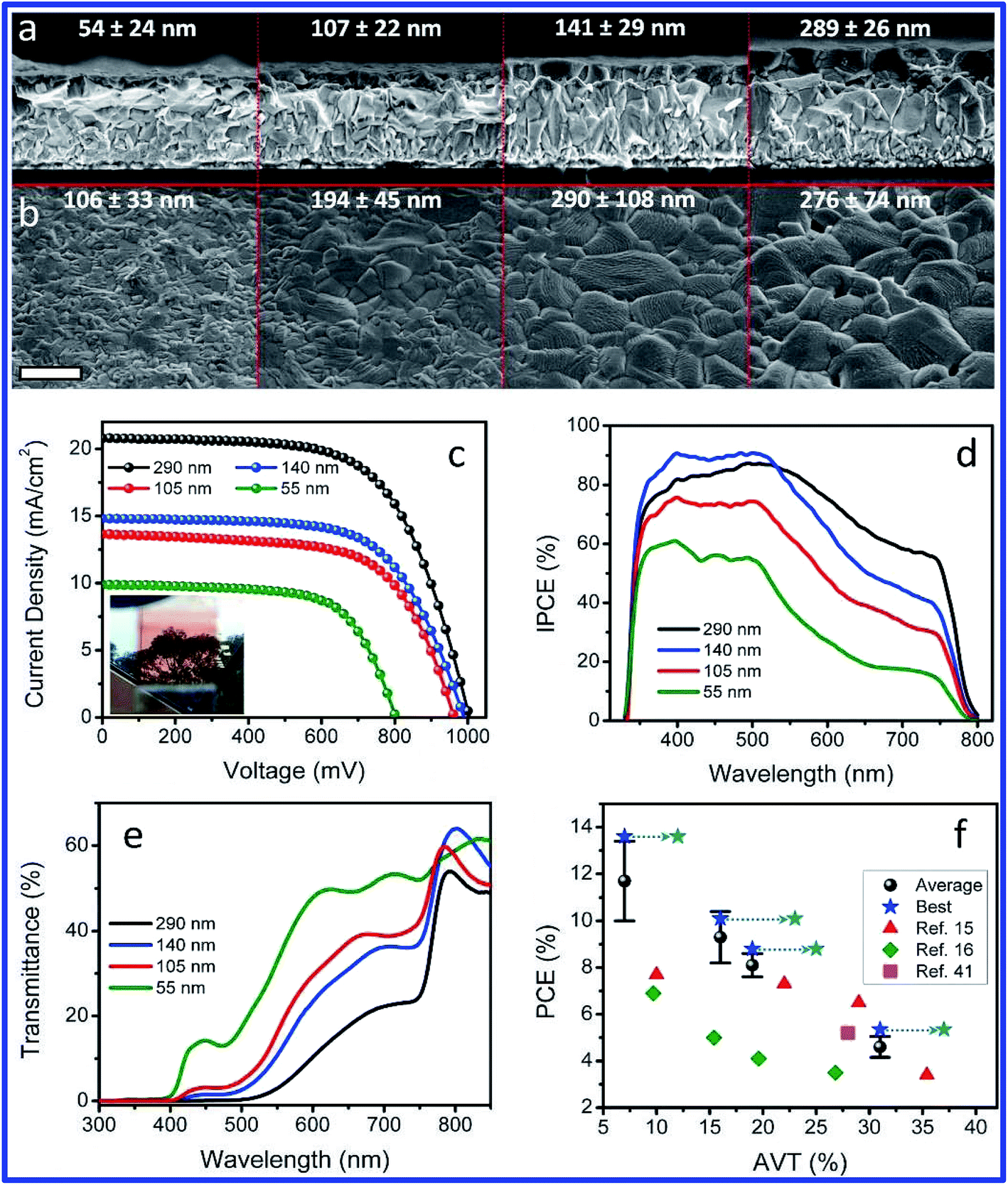 | ||
| Fig. 25 (a) Cross-section SEM (b) top view SEM, (c) current density voltage characteristics, (d) IPCE spectra, (e) transmittance spectra and (f) PCE versus AVT plot for MAPbI3 thin-film solar cells with different absorber layer thicknesses and a DMD cathode,311 presented with permission and copyright. | ||
Eperon et al. investigated the use of formamidinium lead iodide (FAPbI3) as the absorber in an effort to develop neutral-colored semi-transparent PSCs.313 Due to the fact that the formamidinium cation is larger than the methylammonium ion, the energy band gap of FAPbI3 is reduced to 1.48 eV relative to 1.57 eV for MAPbI3. Other advantages of FAPbI3 in PV applications include greater thermal stability and photostability under illumination. A modified excess organic precursor process using both MAI and FAI in the low vapor pressure solvent dimethyl sulfoxide (DMSO) was used to synthesize FAPbI3 films with an island morphology that is favorable for solar energy conversion. The MAI precursor plays a sacrificial role in the synthesis and is supposed to allow a by-product of the reaction to be removed more easily. The two organic precursors MAI and FAI and PbCl2 were spin-coated followed by thermal annealing. To compare the photovoltaic performance of FAPbI3 and MAPbI3 absorbers deposited by this process, two series of semi-transparent planar heterojunction devices with the structure FTO/TiO2/FAPbI3 (or) MAPbI3/spiro-OmeTAD/Au were fabricated. The use of an Au cathode, however, resulted in a non-neutral color.314 Photovoltaic performance parameters extracted from J–V characteristics under 1 sun, AM1.5G irradiance show that the JSC, VOC, FF, and PCE of the FAPbI3 device are all higher than those of the MAPbI3 device. The external quantum efficiency (EQE) spectra show that the higher JSC of the FAPbI3 device is due to a longer cutoff wavelength because of its narrower bandgap. Another important aspect of FAPbI3 is that the J–V characteristics are less prone to hysteresis, and the stabilized PCE is closer to the PCE deduced from a rapid J–V scan. These results show that FAPbI3 is a better absorber for high-performance semi-transparent PSCs.
Low-cost color-neutral semi-transparent FAPbI3 solar cells were realized by Eperon et al. using a transparent conductive laminate cathode consisting of a nickel mesh within a PET film.313 This transparent laminated cathode (TLC) was attached to the device using a pressure-activated adhesive comprising PEDOT:PSS and acrylic glue. The optical properties of the FAPbI3 device with the TLC attached were characterized by optical transmission and measurement of CIE color coordinates. The attachment of the TLC reduces the average transmittance (AVT) of the FTO and the device layers from 34.2% to 28.1%. The color coordinates of light transmitted through the TLC, active layer and FTO substrate are close to that of the incident AM1.5G simulated sunlight. This shows that the semi-transparent FAPbI3 device with TLC is neutral colored. The measured PCE of this neutral colored device based on FAPbI3 is 5.2%, while the AVT is only 28%.
In addition to halide perovskites, non-wavelength selective TPV devices have also been reported using organic semiconductors as an absorber. In ref. 315, Upama et al. fabricated semi-transparent organic solar cells using a bulk heterojunction (BHJ) photosensitive layer comprising a blend of PTB7 (poly{4,8-bis[(2-ethylhexyl)oxy]benzo[1,2-b:4,5-b′]dithiophene-2,6-diyl-alt-3-fluoro-2-[(2-ethylhexyl)carbonyl]thieno[3,4-b]thiophene-4,6-diyl}) and PC71BM ((6,6)-phenyl C71 butyric acid methyl ester). The photosensitive ink containing PTB7 (donor) and PC71BM (acceptor) were first deposited onto ZnO coated ITO substrates through spin coating. This is followed by the deposition of a MoO3 (6 nm)/Ag (7 nm)/MoO3 (40 nm) OMO cathode to enhance transparency. Starting with the optimized thickness of 200 nm for the BHJ layer of opaque devices, the photoactive layer was reduced to 170 nm and 130 nm by varying the spin speed, while the thickness of the MoO3/Ag/MoO3 layers was kept constant. The PV parameters and the AVT of all three devices were measured and compared with simulation. As the BHJ layer thickness decreased from 200 nm to 130 nm, the AVT increased from 18.3% to 24.9%. This increase occurred mainly in the shorter wavelength region (370–600 nm). The PCE of the champion device for each BHJ thickness decreased from 5.00% (200 nm) to 3.82% (130 nm). The decrease in PCE is mainly due to a decrease in JSC resulting from reduced photo-generation of excitons.
Unlike other literature, the CRI of these devices was also reported by Upama et al.;315 when the BHJ layer thickness was increased from 130 to 200 nm, the CRI decreased from 66% to 57%. This shows that there is a separate tradeoff between the PCE and the CRI of these semi-transparent devices. The relatively low CRI is due to strong visible light absorption around 600–700 nm.
7.3. Wavelength selective TPV devices
An early example of a wavelength selective TPV device is the NIR absorbing solar cell with heptamethine dye as an absorber, as reported by Véron et al.316 The heptamethine dye is a member of the polymethine dyes and is cationic. This means that after synthesis, the heptamethine cation must have a corresponding anion to maintain charge neutrality. The chemical nature of the counterion is known to affect the photophysical properties of the heptamethine dye.316Although the optical absorption spectra of compounds 1 and 2 dissolved in various organic solvents are quite similar, the absorption spectra of 20 nm thin films of compounds 1 and 2 deposited on glass substrates were found to be affected by the counterion (Fig. 26a). Compound 1 shows stronger absorption than compound 2 from 550 nm to 900 nm and has an absorption peak at 850 nm that is slightly red-shifted from the absorption peak of compound 2. For both compounds, absorption occurs mainly in the NIR region. Bilayer heterojunction devices with the structure ITO/MoO3/dye/C60/Alq3/Ag/Alq3 were fabricated using both compound 1 and compound 2 for the dye layer (Fig. 26b). For compound 1, the best performing semi-transparent cell has a PCE of 0.9% and an AVT (450–670 nm) of 62%. The corresponding values for the best semi-transparent cell fabricated from compound 2 are 2.2% and 66%, respectively. The maximum transmittance is 75% at ∼590 nm. Since the only difference between semi-transparent cells made from compounds 1 and 2 is the counterion, the counterion influences the PV properties. As shown by the J–V characteristics (Fig. 26c), compound 2 has both higher JSC and VOC. This is attributed to the reduced bimolecular recombination and reduced current shunts. Note that both devices in this work are semi-transparent because of the significant absorption tail in the visible region for both compounds, which thus renders these cells non-neutral colored. Véron et al.316 performed an ion exchange reaction for the I− ion after the Knoevenagel reaction was performed to synthesize the heptamethine dye core. The original I− anion was exchanged by (i) PF6− and (ii) the organic anion Δ-TRISPHAT− (Fig. 26d). These two organic ionic salts are hereafter referred to as compound 1 and compound 2, respectively.
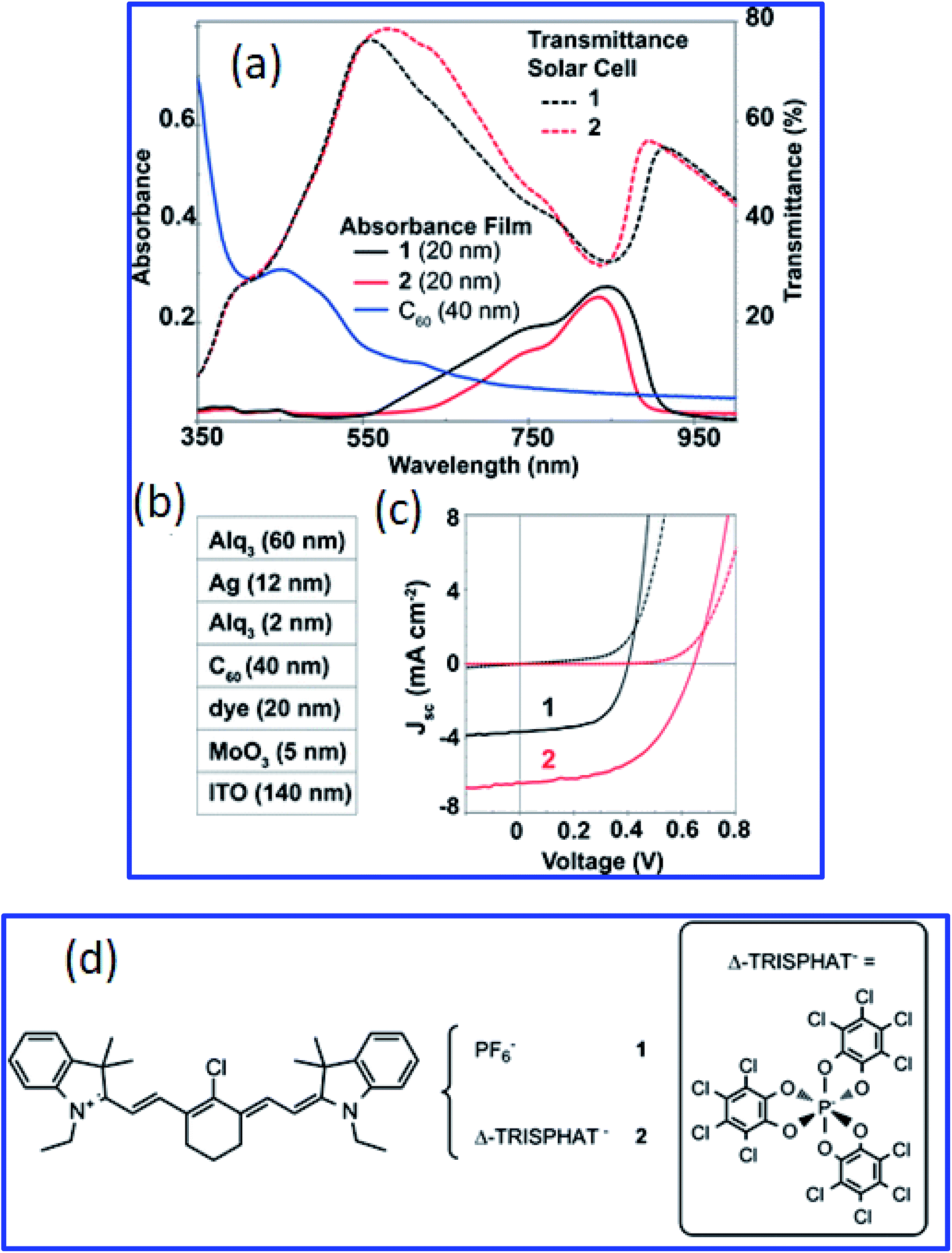 | ||
| Fig. 26 (a) Solar cell transmittance spectra, film absorbance spectra for compound 1 and compound 2, (b) device structure of the semi-transparent NIR absorbing heptamethine dye solar cell, and (c) light and dark J–V characteristics. (d) Molecular structure of the cationic heptamethine dye and the Δ-TRISPHAT− counterion used for the fabrication of non-wavelength selective TPV devices. Both PF6− and Δ-TRISPHAT− are introduced by the ion exchange reaction,316 presented with permission and copyright. | ||
In 2017, Davy et al. reported another organic TPV device to selectively harvest NUV photons in sunlight to generate electrical power for driving an electrochromic window (ECW) device.317 When a bias voltage is applied, the ECW device will darken within seconds because of the electrochromic property of the active layer in the ECW. The combination of wavelength-selective TPV and ECW devices that operate independently at different spectral regions allows smart windows that can actively regulate the amount of visible and NIR light entering a building without using power from the grid to be realized. This can in turn reduce the amount of power used for cooling the building. Both the donor and the acceptor of the small molecule organic heterojunction TPV device fabricated by Davy et al. are functionalized derivatives of a polyaromatic hydrocarbon molecule called contorted hexabenzocoronene (cHBC). The special properties of cHBC include a wide electronic bandgap (3 eV), an extremely high absorption coefficient (200![[thin space (1/6-em)]](https://www.rsc.org/images/entities/char_2009.gif) 000 cm−1) and an absorption maximum at 386 nm.318 The cHBC molecule can be easily functionalized and one donor derivative (D, p-type) and two acceptor derivatives (A1 and A2, n-type) were synthesized. The donor contains oxygen heteroatoms, while both acceptors contain chlorine. Both D and A1 and A2 are thermally stable and can be deposited as thin films by thermal evaporation in a vacuum. The energy levels of the HOMO and the LUMO of the donor and acceptors which are crucial to the design of organic PV devices were measured using UPS and inverse photoemission. The LUMO offset values for D/A1 and D/A2 are 0.5 eV and 0.8 eV, respectively, and are much smaller than the same offset for D/C60, which is 1.4 eV. This small offset results in a smaller energy loss upon exciton dissociation and a cell with higher power output. The absorption coefficient spectra of D, A1, and A2 consist of sharp peaks in the NUV spectral region (372–409 nm) and decrease rapidly beyond 450 nm, suggesting that the donor and acceptors are acting in a complementary manner as NUV selective absorbers.
000 cm−1) and an absorption maximum at 386 nm.318 The cHBC molecule can be easily functionalized and one donor derivative (D, p-type) and two acceptor derivatives (A1 and A2, n-type) were synthesized. The donor contains oxygen heteroatoms, while both acceptors contain chlorine. Both D and A1 and A2 are thermally stable and can be deposited as thin films by thermal evaporation in a vacuum. The energy levels of the HOMO and the LUMO of the donor and acceptors which are crucial to the design of organic PV devices were measured using UPS and inverse photoemission. The LUMO offset values for D/A1 and D/A2 are 0.5 eV and 0.8 eV, respectively, and are much smaller than the same offset for D/C60, which is 1.4 eV. This small offset results in a smaller energy loss upon exciton dissociation and a cell with higher power output. The absorption coefficient spectra of D, A1, and A2 consist of sharp peaks in the NUV spectral region (372–409 nm) and decrease rapidly beyond 450 nm, suggesting that the donor and acceptors are acting in a complementary manner as NUV selective absorbers.
Planar heterojunction solar cells with the structure Si/MoO3/D/A1(A2)/BCP/Al were fabricated to evaluate the PV performance of the D/A1 and D/A2 heterojunctions. The VOC of the devices containing the D/A1 and D/A2 junctions are 1.63 and 1.46 V, respectively, which are much higher than the VOC of the reference D/C60 junction (0.82 V). It is worth pointing out that the VOC of D/A1 obtained in this work is one of the highest reported for any thin-film solar cell. The high VOC exhibited by junctions based on derivatives of cHBC is the direct result of the small energy offset mentioned above and the wide bandgaps of D and A1(A2). The wide bandgap of D and A1(A2), however, also increases the transparency of these layers and reduces the JSC. Despite this, the maximum power obtainable from the D/A1 and D/A2 devices is comparable to that of the D/C60 reference device. The PCE of the D/A1 and D/A2 devices under 1 sun, AM1.5G is in the range of 1.3–1.5%, respectively, and the spectral power responsivity for D/A1 and D/A2 is 12.4% and 14%, respectively.
An area scalable TPV device based on D/A1 was demonstrated by replacing the Si substrate of the planar heterojunction on ITO glass. To reduce the parasitic series resistance, the ITO was coated with a 30 nm thick Ag grid with 97% transparency in the range of 300–800 nm. When the device active area was increased from 1 cm2 to 10 cm2, there is little change in the J–V characteristics under illumination. This shows that the TPV device is scalable to match the ECW device. The area scalability is attributed to the amorphous pinhole-free structure of the cHBC derivative films. Although the AVT of this TPV device was not reported, the transmittance of stacked TPV and ECW devices in the bleached state ranges from 20% to 70% for the spectral range 400–1000 nm.317
Another NUV harvesting air-stable TPV device based on wide bandgap halide perovskite semiconductors was reported by Liu et al. in 2018.319 Although MAPbI3 and FAPbI3 are both excellent absorber materials for high-efficiency thin-film solar cells, their broad absorption bands in the visible region render them less useful in fabricating TPV devices with a high AVT. The highest AVT reported for a semitransparent MAPbI3 device is ∼46%. By substituting the iodide ion by smaller halide ions such as bromide and chloride in MAPbI3, the absorption edge can be shifted towards the UV wavelengths. In ref. 319, two mixed halide perovskites with the general formula MAPbCl3−xBrx (x = 0 and 0.6) were fabricated by solution-based spin coating. However, the process is more challenging than the spin coating deposition of MAPbI3 because of rapid crystallization and limited solubility of MAPbCl3 precursors in solvents. The specific details of the deposition process were found to have a crucial impact on the quality of the resulting halide perovskite films. After investigating various alternative processes, Liu et al. reported that smooth, uniform and transparent MAPbCl3−xBrx films can only be obtained by using a vacuum-assisted solution deposition together with post-deposition through methylamine gas treatment.319 A blue shift in the optical absorption edge was observed as the bromide content x is decreased. As a result, the MAPbCl2.4Br0.6 films deposited by this process appear light yellow, while the MAPbCl3 films are transparent.
TPV devices with the structure ITO/PEDOT/MAPbCl3−xBrx/C60/BCP/Ag/Alq3 were fabricated on ITO glass substrates. Here, BCP is bathocuproine and Alq3 is tris-(8-hydroxyquinoline)aluminum. The PEDOT layer was used as the HTL and C60 as the ETL. BCP was used in conjunction with Alq3 to enhance the transmittance of the top Ag electrode by an OMO thin film structure. The best MAPbCl3−xBrx TPV device displayed a PCE of 0.52%, while the champion MAPbCl3 device had a PCE of 0.32%. This is because of the narrower bandgap of the MAPbCl3−xBrx absorber (2.83 eV) relative to that of MAPbCl3 (3.04 eV), which results in a higher JSC. The AVT of the MAPbCl3−xBrx device and the MAPbCl3 device calculated from the transmittance spectra are 73% and 72.1%, respectively (Fig. 27a and b). These are the highest AVT reported for any TPV device with a transparent active layer. Since both devices are highly transparent in the visible region (Fig. 27c and d), the CRI values are similarly high (94.4 for MAPbCl3 and 93.8 for MAPbCl3−xBrx). These CRI values suggest that light transmitted through these devices can provide the natural color to objects very well (Fig. 27c and d). The main improvement needed for these devices with wide bandgap halide perovskite absorbers includes increasing the internal quantum efficiency which should lead to a higher PCE in the future.
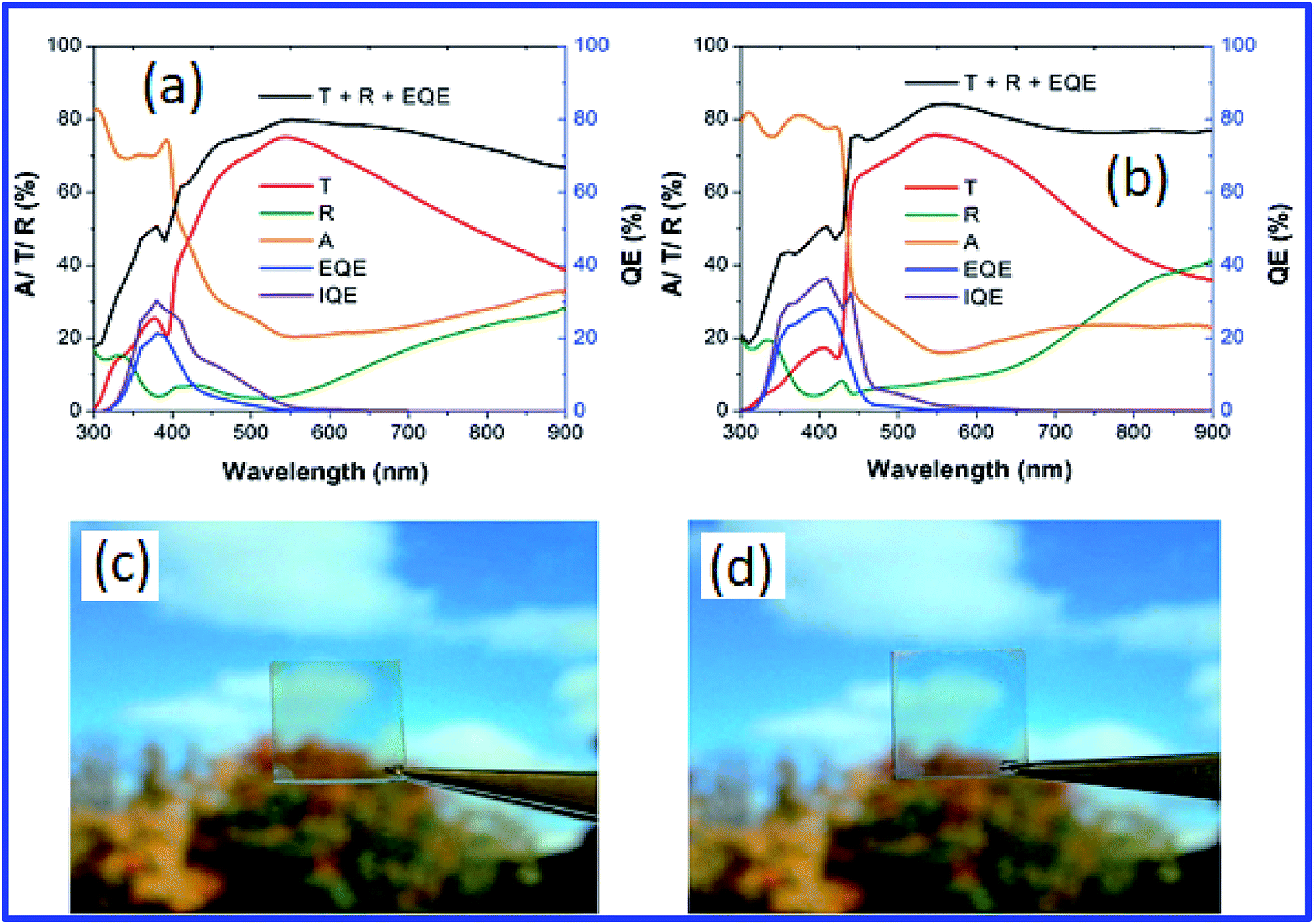 | ||
| Fig. 27 (a) Absorbance, transmittance, reflectance, external quantum efficiency (EQE) and internal quantum efficiency (IQE) spectra of the MAPbCl3 device, (b) absorbance, transmittance, reflectance, EQE and IQE spectra of the MAPbCl2.4Br0.6 device, (c) photograph of the TPV device fabricated from the MAPbCl3 absorber, (d) photograph of the TPV device fabricated from the MAPbCl2.4Br0.6 absorber,319 presented with permission and copyright. | ||
8. SnO2 for energy storage
Energy from sustainable resources has been considered one of the key challenges for the modern society.320 Indeed, a rapid increase in the global population and growing economic expansion significantly increased the energy consumption which heavily relies on sustainable sources of energy materials and devices. Access to green, affordable, and dispatchable energy that can act as a substitute for fossil fuels is urgently needed. The dramatically rising worldwide concerns on the shortage of clean/renewable energies warrant the novel design and development of advanced nanostructured materials towards fabricating stable energy storage devices. In this regard, electrochemical storage plays an increasingly important role in the design and development of sustainable energy technologies. Among the electrochemical storage, batteries and supercapacitors have been heavily investigated by both industry partners and the research community to meet the on-going demands of electronics (consumer/smart/portable), electric vehicles, etc.321–323 The salient differences between batteries and supercapacitors are that they have different storage mechanisms, device configurations, and fabrication procedures. Typically, batteries can provide high energy density, while supercapacitors offer high power density for charge storage.8.1 SnO2 in lithium-ion batteries (LIBs)
Li-ion batteries (LIBs) are regarded as an advanced promising technology among various electrochemical energy storage applications because of their excellent volumetric and gravimetric power/energy density, extremely low self-discharging characteristics, high stability and long life cycle.324 LIBs serve as the dominant power source for a wide range of portable electronics such as mobile phones and laptops.325 However, the practical capacity of conventional LIBs is still far below the current market demand in the field of electric vehicles due to their insufficient energy density. Therefore, the design of new electrode materials for the LIBs using emerging advanced nanostructures with improved characteristics is a prerequisite for their realization in real-time energy storage applications that meet the on-going demand of 2–5 times higher energy density.326 Over the past decade, significant efforts have been devoted to investigating transition metal oxide (TiO2, SnO2, MnO2, and Fe2O3) based anode materials in LIBs owing to their versatile tunable physical/chemical properties with promising electrochemical performances. Some of the representative specific capacities of nanostructured materials (anode based) include graphene (960 mA h g−1),327 CNTs (1100 mA h g−1),328 porous carbon (1100 mA h g−1), silicon (4200 mA h g−1),329 and transition metal oxides (500–1000 mA h g−1)330 among others. However, inherent limitations of the anode materials such as high volume variation during charging/discharging, capacity fading due to solid-electrolyte interphase (SEI) films, poor electrical conductivity, and low coulombic efficiency must be overcome before these newer anode materials can effectively function in practical LIBs.Metal-oxide based and sulfide based electrode materials such as molybdenum disulfide (MoS2),331,332 manganese dioxide (MnO2),333 ferric oxide (Fe3O4),334,335 and cobalt tetraoxide (Co3O4)336 based nanostructured composite materials have been widely studied as storage materials in LIBs because of their abundance, the high theoretical capacity of 992 mA h g−1 and the low-working potential (0.6 V).337–343 In recent years, SnO2 has garnered considerable attention due to its abundance, low-cost, biological compatibility, and high theoretical/specific capacity (1494 mA h g−1) (as against graphite (342 mA h g−1)).343 SnO2 based materials have gained momentum as an alternative anode material in LIBs since the pioneering work of Idota et al. more than two decades ago (1997) who reported a reversible capacity of 600 mA h g−1.344 Typically, SnO2 undergoes 2 major steps in the reaction with lithium ions (Li+) that includes the conversion reaction and the alloying/de-alloying process.345,346
| SnO2 + 4Li+ + 4e− → 2Li2O + Sn | (1) |
| Sn + xLi+ + xe− → LixSn (0 ≤ x ≤ 4.4) | (2) |
| LixSn → Sn + xLi+ + xe− (0 ≤ x ≤ 4.4) | (3) |
To further improve the surface area and specific capacity of SnO2 based active materials, several strategies have been devised in tuning the morphology and nanostructuring at the nanoscale through hybridization of SnO2 with various suitable supports such as metals, carbon nanostructures, metal sulfides/phosphides/chalcogenides, conducting polymers, etc.347–349 For instance, compositing with carbon nanostructures (CNTs, graphene, fullerenes) not only helps to tackle the volume expansion during charging/discharging but also serves to improve the overall conductivity.350 Various design strategies/principles of nanostructured SnO2 (nanoparticles/nanocrystals, nanoflowers, nanotubes, nanoplates, nanospheres, nanowires, quantum dots, etc.) have been employed to fabricate robust SnO2 based anodes, which are considered as one of the promising routes for achieving high coulombic efficiencies and high-specific capacities in LIBs.351–355
The majority of the work focuses on modifying SnO2 with various carbon nanomaterials (graphene, mesoporous carbon, CNTs, etc.) with the aim of constructing robust and stable LIBs.338,356–359 For example, a 2D porous carbon-coated sandwich structure featuring mesoporous SnO2/graphene/SnO2 nanosheets (C@SnO2–rGO–SnO2) has been rationally designed and fabricated through combined hydrothermal and template-assisted nanocasting impregnation strategies. Wang et al. demonstrated enhanced Li storage capacity in LIBs by judiciously considering the inherent beneficial properties of individual components (Fig. 28).356 The authors took advantage of the nanocrystal size and mesoporous structure to design this type of unique hybridized system through utilizing SiO2–rGO–SiO2 as a template. The electrochemical performances of various hybrids were compared (GO/SnO2, GO–SnO2@C, mesoporous SnO2–rGO–SnO2 (c), and porous C@SnO2–rGO–SnO2) and their reaction mechanisms were presented for the lithiation/delithiation processes. Among the investigated electrode materials, C@SnO2–rGO–SnO2 exhibited excellent reversibility, high rate performance (315 mA h g−1 at 10 A g−1), and extended cyclability (525 mA h g−1 after 1200 cycles at 2 A g−1).
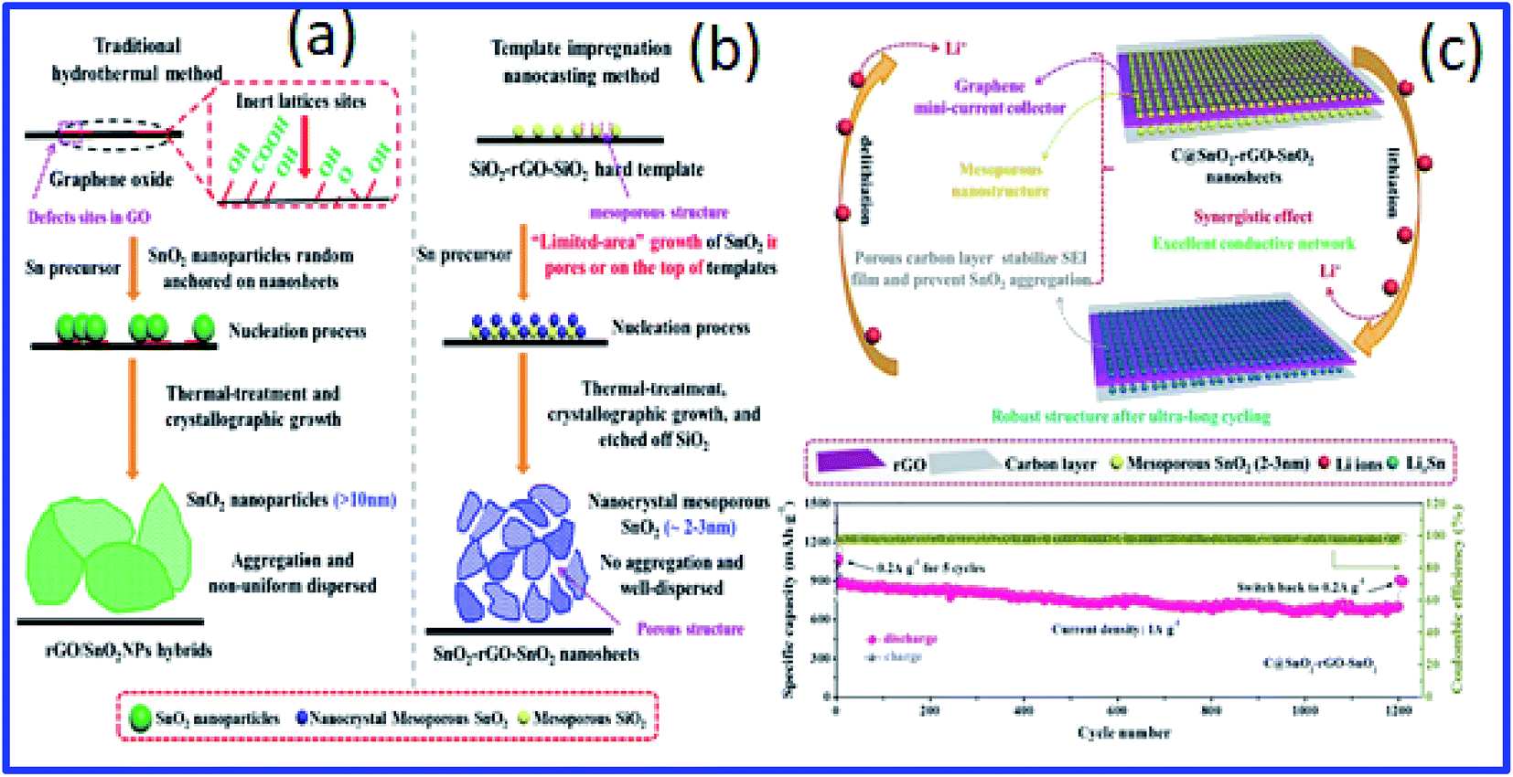 | ||
| Fig. 28 Schematic representation of the research methodology adopted for the (a) hydrothermal method, (b) nanohard template casting method, and (c) charge/discharge profiles of C@SnO2–rGO–SnO2 at a current density of 1 A g−1,356 presented with permission and copyright. | ||
In another interesting report, monodispersed ultra-small (∼5 nm) nanocrystals of SnO2 (74.85 wt%) were uniformly distributed on co-doped nitrogen/sulfur graphene sheets (NSGS) using the layer by layer (LBL) assembly strategy towards the fabrication of high-performance LIBs with high discharge capacity (2123 mA h g−1 at 0.1 A g−1), extended cyclability (99.2% after 500 cycles), and rate capabilities.338 Besides, the authors also tested the optimized electrode system (NSGS-8) in Li half/full fuel cells and systematically investigated their electrochemical reaction kinetics. Similarly, hollow SnO2 nanospheres (positively charged) with oxygen vacancies encapsulated by a nitrogen-doped network of graphene (negatively charged) (SnO2−x/N-rGO) have been prepared by the electrostatic adsorption-induced self-assembly and further tested for their practical utility in LIBs (Fig. 29a–d). Fig. 29b depicts the HR-TEM image of SnO2−x/N-rGO showing lattice fringes with the interplanar distance (0.33 nm) corresponding to tetragonal SnO2. The charge/discharge profile and the cycling performance of the investigated materials (bare and carbon-based anodes) and the remarkable rate capability (309 mA h g−1 at 10 A g−1) and robust stability (912 mA h g−1 even after 500 cycles) (Fig. 29c and d) exhibited by the as-constructed nanostructured SnO2 entrapped by an N-doped graphene composite network envisage the potential prospects of SnO2 in advanced LIBs.357
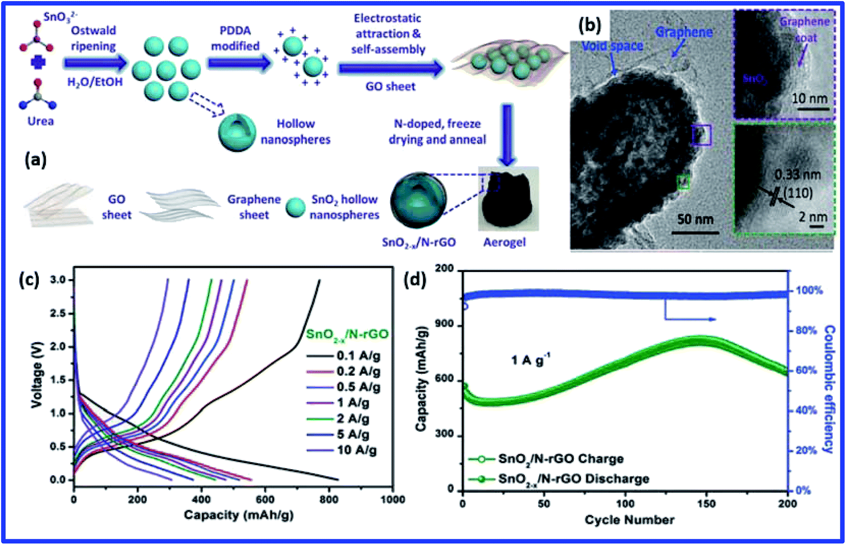 | ||
| Fig. 29 (a) Scheme showing the preparation of a 3D hierarchical SnO2−x/N-rGO network. (b) TEM images, with the insets showing the HRTEM images, (c) charge–discharge profiles, and (d) cycling performance (0.1 A g−1) of SnO2−x/N-rGO,357 presented with permission and copyright. | ||
In LIBs, SnO2 is well established as an anode material. However, there are reports where SnO2 nanoparticles were used to modify the conventional cathodes such as lithium cobalt oxide (LCO)360 and lithium nickel cobalt manganese oxide, LiNi1/3Co1/3Mn1/3O2 (LNCMO).361 Ma et al. demonstrated that a thin layer of SnO2 coating on LiNi0.5Mn1.5O4, LNMO, by a facile synchronized coating strategy can enhance its electrochemical performance.362 With the help of these coating strategies, they not only were able to coat a thin layer of SnO2 on the surface of the LNMO but also a very small amount of Sn2+ ions can enter the spinel to stabilize and modify the spinel structure.362 The battery performance demonstrated that the specific capacity at a lower current rate of 0.2C of LNMO@SnO2 is much higher than that of the pristine LNMO. For the pristine LNMO, the material is derived from calcination of the precursor at a high temperature. At that temperature, the Ni solubility in the LNMO spinel lattice will decrease and a reduction of Mn4+ to Mn3+ took place, which resulted in the formation of a NixLiyO impurity phase. Thus, the obtainable specific capacity of pristine LNMO was lower due to the presence of the NixLiyO impurity phase, and a given amount of Mn3+ also existed in the spinel due to charge neutrality, which is different from the ordered P4332 structure of stoichiometric LiNi0.5Mn1.5O4. For LNMO@SnO2, the Sn2+ doping would inhibit the formation of the inactive NixLiyO impurity phase owing to its structural stabilization effect. As a result, the reduction of Mn4+ to Mn3+ in the spinel was inhibited. This decreased content of inactive NixLiyO was responsible for the increased specific capacity of the LNMO@SnO2. Besides, the rate performance and the cycling performance of the LNMO@SnO2 were also superior to those of the pristine LNMO. The improved cycling performance of LNMO@SnO2 should be attributed to the surface SnO2 coating layer, which alleviated the interaction between the active material surface and the electrolyte and suppressed the excessive formation of a thick SEI film.
For the superior performance of a LIB, the electrolyte affinity and the thermal stability of the separator are very crucial. In a report, Xiang and co-workers functionalized a polyethylene (PE) separator through binder assisted coating using hollow SnO2 nanoparticles of size around 250 nm and investigated this functionalized PE separator and LIBs systematically.363 It was observed that the SnO2 functionalized PE separator not only enhanced the electrolyte wettability but also can withstand a temperature of 130 °C, which means that the functionalized PE separator can uptake a higher electrolyte content as a result of which a high rate performance and charge–discharge performance at elevated temperatures were achieved. To evaluate the battery performance of the functionalized separator, it was tested with LiCoO2 half cells at room temperature and 80 °C. At room temperature, both the pristine and functionalized separators showed similar initial discharge capacity as well as similar capacity retention after 100 cycles. However, when the half cells were tested at 80 °C, it was observed that the efficiency of the pristine separator declined rapidly after the 70th cycle, whereas the functionalized separator was stable even after 70 cycles throughout the testing period at 80 °C. This could be attributed to the localized deficiency of the electrolyte in the pristine separator during high temperature cycling of the battery. As the cycling goes on, the electrolyte may redistribute in the battery and the capacity of the battery is partly recovered. The excellent half-cell performance of the SnO2 functionalized separator demonstrates the hypothesis that the SnO2 coating layer enhances the electrolyte retention of the PE separator at elevated temperatures.363
In yet another interesting report, a general route for the facile, cost-effective preparation of metal oxide (TiO2/SnO2)/MXenes has been reported by Gogotsi et al. through self-assembling SnO2 nanowires on MXene nanosheets through van der Waals interactions towards fabricating high power/energy, superior rate performance and stable energy storage in LIBs (Fig. 30).347 Herein, MXenes (Ti3C2) play the role of a conductive additive to mitigate the agglomeration of SnO2. On the other hand, the use of SnO2 avoids the precipitation and restacking of MXene nanosheets during the Li insertion/extraction process. A high capacity of 530 mA h g−1 was observed even after 500 cycles. The comparison of rate capabilities reveals that the as-fabricated SnO2/MXene heterostructures delivered superior capacities of 720, 665, 606, 560, 489, and 310 mA h g−1 at current densities of 100, 200, 500, 1000, 2000, and 5000 mA g−1, respectively, over their non-modified SnO2 and MXene counterparts. The reduced pathway for lithium diffusion and enhanced active area have been observed to contribute to the remarkable electrochemical performance in the fabricated LIBs.
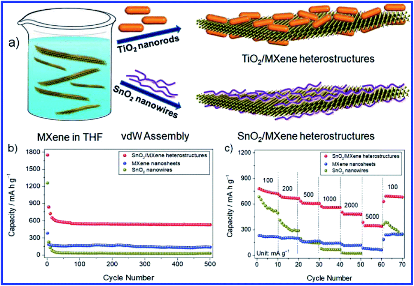 | ||
| Fig. 30 (a) Scheme showing the self-assembly on MXene nanosheets, (b) their specific capacities at a current density of 1000 mA g−1 and (c) rate capabilities for 70 cycles,347 presented with permission and copyright. | ||
8.2 SnO2 in lithium–sulphur batteries (LSBs)
Lithium–sulphur (Li–S) batteries are also considered as the future of energy storage devices owing to their high theoretical capacitance (∼1680 mA h g−1 for sulfur and 3860 mA h g−1 for lithium).364 Considering an average voltage window of 2.15 V, the theoretical specific energy density of the Li–S batteries was estimated to be ∼2500 W h kg−1, which is beyond that of conventional LIBs (∼400 mA h g−1). Also, sulfur is cheap and earth-abundant, making Li–S batteries a promising low-cost technology for widespread usage. Owing to the strong adsorption capability of lithium polysulphides, SnO2 has been used as a cathode to trap lithium polysulphide which in turn not only reduces the shuttling effect but also enhances the overall performance of the Li–S batteries.365Fig. 31 presents the schematic representation of conventional LIBs, conventional Li–S batteries and SnO2 modified Li–S batteries.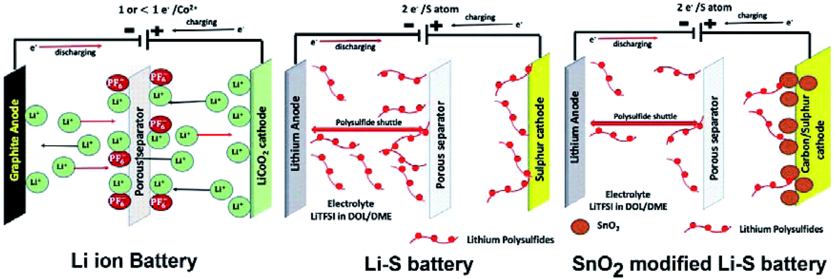 | ||
| Fig. 31 Schematic of conventional LIBs, Li–S batteries and SnO2 modified Li–S batteries. | ||
Different from others, Yu et al.366 used an rGO/SnO2/S composite prepared via a one-pot hydrothermal method for use as a cathode and obtained an initial discharge capacity of 1592 mA h g−1 at 0.1C which stabilized to 607 mA h g−1 at 0.2C over 100 cycles which is more than that of the rGO/S cathode (508 mA h g−1 at 0.2C over 100 cycles) and the pristine S cathode electrode (388 mA h g−1 at 0.2C over 60 cycles). Fig. 32a presents the schematic representation of SnO2 as a polysulphide immobilizer. From the high resolution transmission electron microscopy (HRTEM) image presented in Fig. 32b, it can be observed that 5 nm SnO2 nanoparticles are embedded in rGO sheets along with the loading of synthesized sulfur. The elemental mapping further confirmed the presence of Sn, C, O, and S (Fig. 32c). The formation of lithium polysulphide and lithium sulphide was observed from the cathodic peak position at 2.3 V and 2.0 V in the cyclic voltammetry (CV) curve presented in Fig. 32d. During the anodic process, lithium sulphide first converts into lithium polysulphide and then to S, which was confirmed from the presence of anodic peaks at 2.3 V and 2.4 V, respectively. No redox peaks were observed between 1.7 V and 2.8 V, which confirmed that SnO2 does not take part in the redox reaction and only acted as a polysulphide immobilizer. From Fig. 32e and f, it can be derived that SnO2 has a positive influence on the electrochemical performance of the rGO/S cathode. The prepared electrode (rGO/SnO2/S) showed a discharge capacity of 575 mA h g−1 at 5C, showing its excellent rate capability. In the same way, Wang et al.367 synthesized SnO2 nanosheets on a carbon cloth, which demonstrated a specific discharge capacity of 1228 mA h g−1 at 0.2C which is more than that of the sulfur cathode on a carbon cloth (600 mA h g−1 at 0.2C). The SnO2/carbon cloth cathode retained 76% capacity over 1000 cycles at 2C. There are reports where SnO2 was coupled with carbon nanostructures like carbon nanotubes, carbon radial nanorods, carbon hollow spheres, carbon aerogel and sulfur to form the cathode material of Li–S batteries.368–376 In all these reports, SnO2 was used to trap lithium polysulphide to mitigate the shuttling effect and ensure better utilization of active sulfur in the cathode.
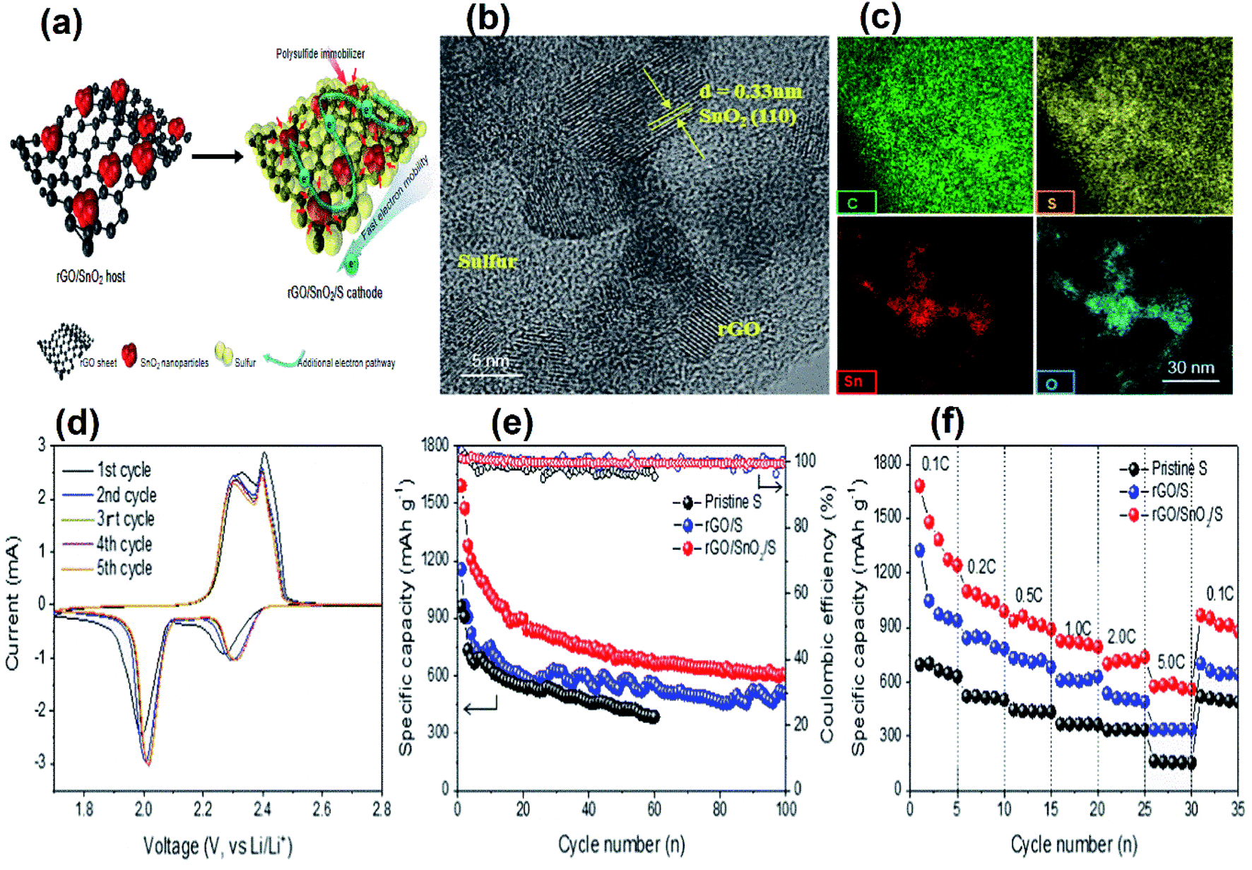 | ||
| Fig. 32 Schematic representation of the rGO/SnO2/S cathode acting as a polysulphide immobilizer (a); HRTEM image (b) and elemental mapping (c) of the rGO/SnO2/S composite; cyclic voltammetry curve at 0.1 mV s−1 (d); and cycling performance (e) and rate performance (f) of the rGO/SnO2/S composite.366 Adapted with permission of Elsevier. | ||
8.3 SnO2 in supercapacitors
Supercapacitors have drawn substantial interest as an energy device among researchers, specifically due to their high power density and long life cycle bridging conventional dielectric capacitors (which possess high power density) and batteries (which provide high energy density).377,378 There has been achievable progress in the design and development of electrode materials for printable/wearable electronics with enhanced capacitance and extended stability.379–382 However, advanced research is highly warranted for improving the energy density and storage capability in real-life applications such as hybrid vehicles, smartphones, and other energy storage devices in meeting the growing energy demand.383,384 The most commercially successful electrode materials in supercapacitors are carbon-supported metal/metal oxide composites.385,386 Typically, the high surface area can facilitate electrolyte ion transport onto the active sites of the electrode materials, resulting in enhancement of the electrochemical performance. Despite the advantages of carbon-based materials, electrical double-layer capacitors (EDLCs) show relatively low capacitance and limited energy density. Another strategy is to incorporate the carbon materials with metals, metal oxides, or metal-based alloys which can provide a far higher theoretical capacitance in supercapacitors.386,387 These metal/metal oxide loaded active materials in supercapacitors are commonly termed as pseudo-capacitors, which can electrochemically store a large number of electrolyte ions, resulting in higher specific capacitance than EDLCs. However, the pseudo-capacitors suffer from dramatic capacitance fading in long cycles due to the reaction between the surface of active sites and electrolytes.Recent advances in electrode materials in supercapacitors include the mixing of carbon and non-carbon-based materials to maximize the performances of these two types of materials. In this regard, hybrid electrode materials with numerous combinations involving carbon-based materials (graphene, CNTs, porous carbon, fullerenes) and metal oxides such as tin oxide,388 ruthenium oxide,389 manganese oxide,390 nickel-cobalt hydroxide,391 cobalt oxide,392 and iron oxide393 are highly promising toward the fabrication of next-generation supercapacitors. Hence, improving the inherent materials properties by carefully fine-tuning the components involved in the electrode preparation is highly important in realizing stable and efficient energy storage materials.
Among the host of available metal oxides,39,216,394–400 tin oxide (SnO2) is a wide-bandgap n-type (3.6 eV) semiconducting material with excellent electrochemical properties (high theoretical capacity (782 mA h g−1), redox potential, good electrical conductivity (21.1 ohm−1 cm−1) and thermal stability (>600 °C)) leading to promising applications in a wide range of energy technologies.401 The charge storage mechanism of SnO2 as an active electrode material in an aqueous electrolyte can be written as402
| SnO2 + H+ + e− ↔ SnOOH | (4) |
The utilization of nanostructured SnO2 with tailor-designed morphologies (nanocubes, nanotubes, etc.) has been studied widely in supercapacitors.403–405 For example, nanocomposites made of a low-cost, eco-friendly carbon source (lignin-based multichannel carbon nanofibers) and SnO2 (MCNFs@SnO2) with varied microstructures were prepared by Han et al., through the electrospinning technique (heat-/acid-treated) and heir energy storage capability in supercapacitors was evaluated.406 The stages involved in the fabrication of MCNFs@SnO2 are presented in Fig. 33. A range of different electrode materials were prepared and it was found that the optimized MCNFs@SnO2-5 displayed a high specific capacitance of 128 F g−1 even at a high current density of 50 A g−1. It was found that the inclusion of SnOx (after Sn washing in an acid solution) in MCNF-5 (MCNFs@SnO2-5) resulted in a dramatic increase in capacitance (from 202 to 406 F g−1 at 0.5 A g−1) with extraordinary capacity retention (95% after 10000 cycles, 10 A g−1). This remarkable improvement in the performance of MCNFs@SnO2-5 was due to the following reasons: (i) among the prepared nanocomposites, MCNFs@SnO2-5 has the largest surface area and the total pore volume of 659 m2 g−1 and 0.56 cm3 g−1 with a very narrow pore size distribution; as a result, these mesopores not only reduced the ion diffusion resistance but also improved the kinetics of the electrodes; (ii) synergistic compatibility of the ideal electrical double layer capacitor (EDLC) and pseudocapacitance components in the form of MCNFs and SnO2. The authors claim that the observed values were superior to those of previously reported doped carbon–SnO2 based electrodes that include N/S doped porous carbon nanosheets (willow catkins),407 SnO2 nanorod/rGO,408 SnS2–SnO2 nanocomposites,409 SnO2 dots/activated porous carbon nanofibers,410 N-doped carbon nanosheets (silk),411etc. Carbon/metal-oxide supported SnO2 based active materials pertaining to supercapacitors can also be found elsewhere [ZnO/SnO2,412 Co3O4–SnO@SnO2,413 MnO2@SnO2,414 Ni/SnO2,415 and graphene/SnO2/polypyrrole416].
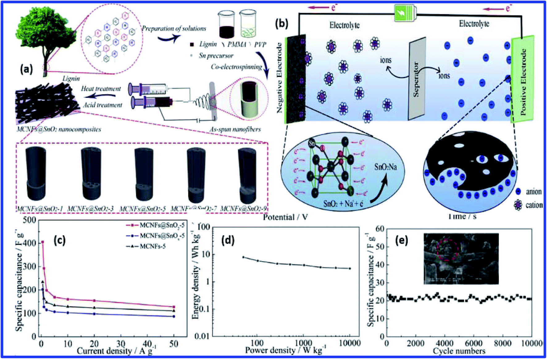 | ||
| Fig. 33 (a) Fabrication steps for MCNFs@SnO2, (b) proposed charge-storage mechanism, (c) current density vs. specific capacities for various electrodes, (d) Ragone plot, and (e) cyclic performance of symmetric capacitors of MCNFs@SnO2-5 at 1 A g−1 (inset: SEM image of MCNFs@SnO2-5),406 presented with permission and copyright. | ||
Several researchers utilized the combination of carbon nanofibers with heterostructures of SnO2 to tailor-design the morphology and compositional engineering through adopting various performance improvement strategies. For example, Ding et al. prepared a porous CNFs/SnO2 membrane with a high specific surface area (1415 m2 g−1) through adopting sequential electrospinning, in situ-polymerization, and calcination, which displayed a high specific capacitance of 118 F g−1 (0.5 A g−1) and excellent cycling durability.417 In the same way, Shao et al. fabricated heterostructured CNFs/SnO2via electrospinning and the solvothermal method and observed superior electrochemical properties due to the low resistance and rapid ion penetration.418 To overcome the conductivity issue of bare SnO2,419 a high energy density and high rate capability flexible supercapacitor based on highly porous, low-cost, and environmentally benign materials such as additive-free 1-D SnO2/carbon nanofibers containing self-assembled closely packed spherical uniform nanoparticles (SnO2@C) on a carbon cloth has been designed through a facile electrospinning technique followed by calcination at different temperatures (400 and 600 °C).420 Interestingly, the obtained energy density for SnO2@C (152 W h kg−1) is much higher than that reported in other similar works.418,421 Among the investigated electrode materials, SnO2@C with SnO2-600 displayed high capacitance (∼646 F g−1 at 60 F g−1), energy density and power density (39 kW kg−1) with excellent cyclability (charge–discharge) (after 10000 cycles at a high current density of 80 A g−1).
Long et al. integrated a range of SnO2 dots supported and uniformly distributed activated porous carbon nanofibers (CNFs) (APCNFs) (using hard templating) on a nickel foam collector for their practical utilization in high-performance adhesive-free flexible supercapacitors,410 and the electrochemical energy storage capability of bare CNFs and SnO2 was compared with that of APCNFs/SnO2. The inclusion of SnO2 dramatically improved the electrochemical performance of the resultant electrode, APCNFs/SnO2, because of the synergistic effect between SnO2 and APCNFs, offering fast electron transfer and ion penetration during charge/discharge processes. The as-constructed electrode displayed high energy and power densities of 10.3 W h kg−1 and 325 W kg−1, respectively, which are sufficient enough to light a red-color indicator connected in series of 1 × 1 cm2 (asymmetric) with high tensile stress and better mechanical strength. Even after testing at a high bending angle (45 to 180°), negligible degradation was observed (Fig. 34).
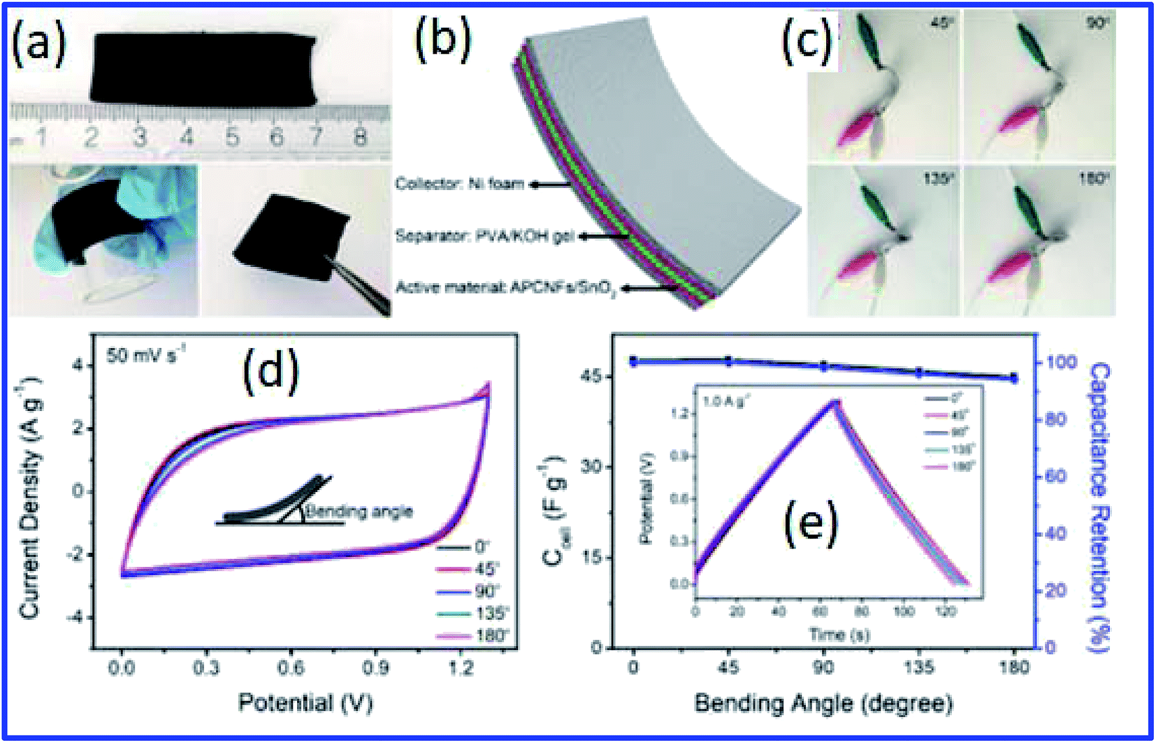 | ||
| Fig. 34 (a) Flexible APCNFs/SnO2 membrane, (b) sandwich-type symmetric cell, (c) optical image, (d) CV curves and (e) specific capacitance and capacity retention at various bending angles (inset: their corresponding galvanostatic charge–discharge profiles),410 presented with permission and copyright. | ||
In another interesting report, Amreesh Chandra et al. devised a universal strategy and proposed a growth mechanism (solid/hollow) of hollow structured metal oxides (simple binary to complex ternary oxides as well) as an emerging electrode material for next-generation supercapacitors.422 The authors have prepared a range of metal oxide nanostructures that include SnO2, Cu2O, Co3O4, and Fe2O3, among others, and found that the unit cell parameters do not differ for solid and hollow type nanoparticles. Subsequently, the as-developed solid and hollow types of metal oxides were tested for supercapacitors through conventional electrochemical measurements. Hollow structuring of metal oxides displays much improved electrochemical performance (close to 2-fold) primarily due to increased redox activity and surface adsorption active sites. The authors envisage that this type of nanostructuring will outperform other similar energy storage systems (electrode materials based on graphene, conducting polymers, etc.).
The combination of electrochromism and supercapacitors offers a new class of devices referred to as electrochromic supercapacitors (ECSs), which can directly indicate their energy storage level through changes in color. This feature allows users to straightforwardly determine the real-time status of the device without using additional instruments and provides visual warnings to prevent overcharging. Electrochromic (EC) chromophores, the core materials of ECSs, chemically store injected charges via electrochemical charging/discharging processes. Simultaneously, optical modulation occurs through electrochromic transitions. As an electrochromic supercapacitor material, tungsten oxide (WO3) is most extensively studied.423–426 However, in all these reports, FTO has been used as the TCO. In a recent study by Jo et al.,427 the authors had demonstrated a novel method of increasing the F doping content in FTO films and its application in the field of electrochromic energy storage devices. The doping content of F was increased by varying sodium hydroxide (NaOH), which acted as a functional additive to the precursor solution during spray pyrolysis. An increase in the F-doping concentration in NaOH modified FTO films enhanced the carrier concentration as well as surface densification that was beneficial to Hall mobility, resulting in a lower sheet resistance (Rsh) of the NaOH modified FTO films. As a result of the improved conduction in the NaOH modified FTO films fabricated with the volume percentage of 5 vol%, the films showed enhanced electrochromic (EC) performances, fast switching speeds (6.6 s for coloration speed and 5.4 s for bleaching speed) and a superb coloration efficiency (CE) of 58.1 cm2 C−1. The fast-switching speeds were caused by the accelerated Li+ and electron transport in the active electrodes due to the decreased Rsh and a superb CE value was generated from the broadened ΔT as an effect of increased electrochemical activity. In addition to EC performance, the enhanced electrochemical activity induced by the decreased Rsh of modified FTO films resulted in efficient transport of a large quantity of Li+ and electrons into the active electrodes, bringing about improved energy storage performance, e.g. a higher specific capacitance (65.2 F g−1 at 2 A g−1), which was clearly evident from the CV, charge–discharge and EIS profiles of WO3 nanostructures on both bare FTO and NaOH modified FTO films.
The electrochromic properties of SnO2 have been well known since the early 2000s.428–431 There are reports on the electrochromic performance of not only SnO2 nanostructures431 but also the doped SnO2 (ref. 430 and 431) and SnO2 based heterostructures with other metal oxides like NiO, WO3, and TiO2.428,429,432,433 However, it came to our notice that the transition metal oxides like NiO, TiO2, and WO3 used to design heterostructures along with SnO2 to study the electrochromic performance of the heterostructures are promising supercapacitor electrode materials. Despite the existence of these heterostructures, the field of electrochromic energy storage devices is mostly dominated by WO3 based electrodes. Thus, these heterostructures can be more efficient than WO3 nanostructures because of their superior pseudocapacitive behavior, and these heterostructures will be crucial in developing the electrodes for electrochromic energy storage devices.
9. SnO2 in circular Economies
Tin has been in use since ancient times, and it has played an important role in the history of the technological race. Over the centuries, tin has become an indispensable ingredient in modern life, supported by mobile devices, solar cells, and wearable devices. The worldwide tin consumption reached 400000 tons per year, powered by a global boom in consumer electronics and a rapid transition to the use of lead-free solders. Hence, in recent years, recycling methods of tin are on the rise. Nearly 30% of the total tin used is derived from electronic waste or e-waste. It is also called ‘urban mining’ and has gained momentum in different countries, thus generating 70000 tons of recycled tin. The circular economy is a way towards the management of waste and pollution, keeping materials in use and regenerating natural systems. It engages a closed loop system, which involves recycling, sharing, repair, refurbishment, and remanufacturing, to reduce the resource usage, waste creation and carbon footprint. The recovery of Sn or SnO2 by a novel CH4 reduction method has been reported using thermodynamic simulations and density functional theory.434 The experiment suggests that CH4 actively reduces SnO2 at 1000 °C to produce high purity Sn. The reported reduction method supports a circular economy through a cost-effective recycling strategy. Fig. 35 shows the mechanism involving the energetics of SnO2 reduction by surface-bound CH4. The method suggests the efficient and economic recovery of a metal element from metal oxide waste.
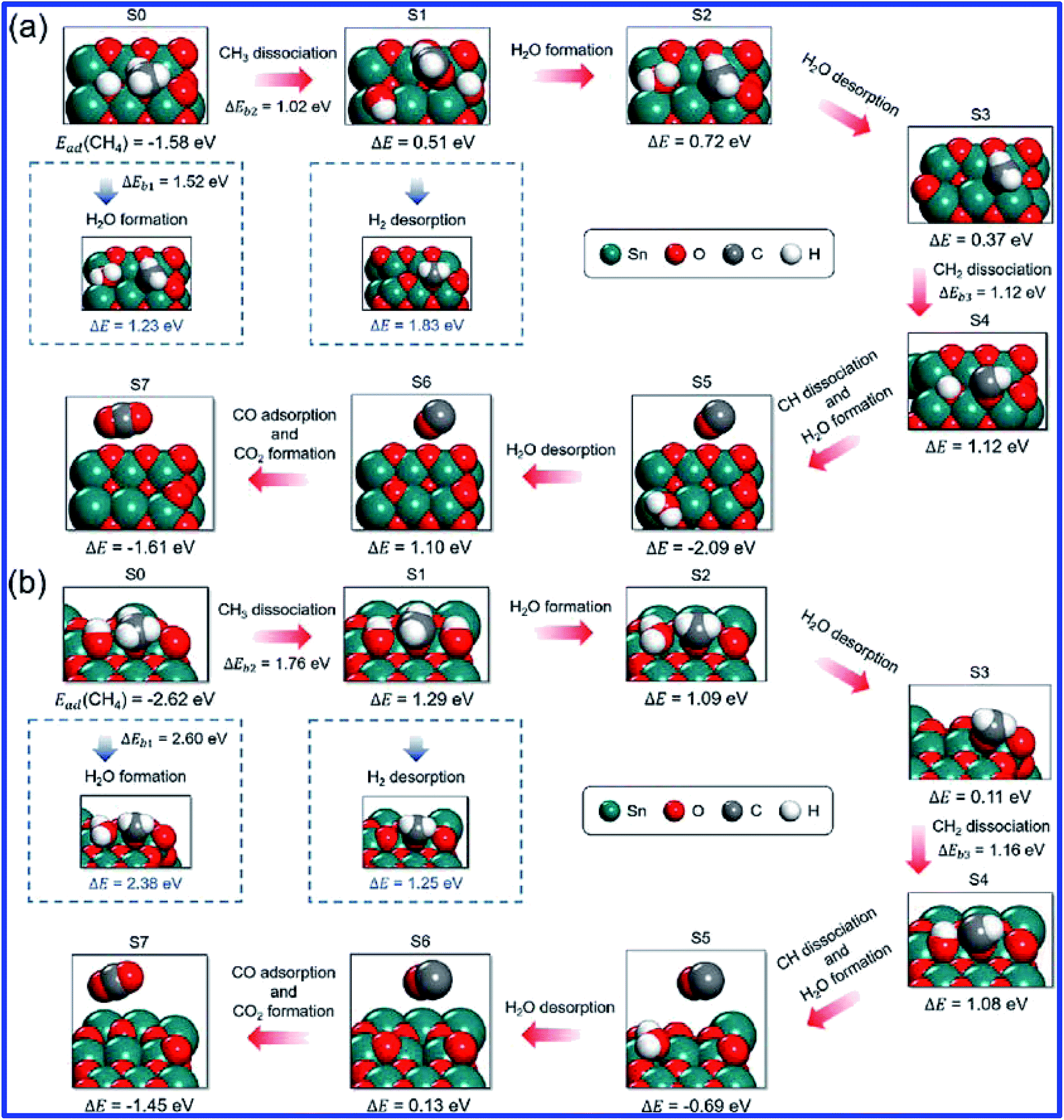 | ||
| Fig. 35 Energetics of SnO2 reduction by surface-bound CH4. (a) SnO2 (100) surface. (b) SnO2 (110) surface. On both SnO2 facets, the formation of H2O was energetically preferred to H2. The red arrows present the preferred reaction pathway. Ead(CH4) represents the adsorption energy of CH4 on the SnO2 surfaces. ΔE of each step represents the energetic state of the current state relative to the previous state. For example, ΔE = 0.51 eV of S1 in (a) means that 0.51 eV of energy is required for CH3 dissociation from S0 to S1,434 presented with permission and copyright. | ||
In another report, the synthesis of cambered nano-walls of SnO2/rGO materials using a melamine template has been reported (Fig. 36). Melamine acts as an ideal recyclable template due to its good adsorbent capacity for M(x)–SnO2/rGO and precipitation after cooling.
 | ||
| Fig. 36 SEM images of (a) SnO2/rGO and (b) M(2)–SnO2/rGO. (c) HRTEM image,435 presented with permission and copyright. | ||
The thickness of SnO2/rGO nano-walls was controlled by varying the melamine content. The synthesized SnO2/rGO showed a reversible capacity of −998 mA h g−1 at a current density of 100 mA g−1 and a capacity of 855 mA h g−1 in a 0.02 to 3.0 V potential vs. Li/Li+. Cambered nano-walls facilitated fast solid diffusion and an efficient liquid channel to improve the reversible capacity. The method is scalable and applicable to other graphene-based energy materials.435 The synthesis route is easily scalable, cost-effective, environmentally friendly, and energy-efficient. Resource-saving, economic and eco-friendly recycling of SnO2/Sn3O4 from Sn anode slime for the development of gas sensing materials is illustrated in Fig. 37.436 Sn anode slime, a by-product of Sn plating, has gas sensing capabilities. Ag-doped SnO2/Sn3O4 as a sensing material for formaldehyde gas was synthesized using the dipping route. At 2 mol% of Ag/Ag2O-doped SnO2/Sn3O4, good sensing properties were observed at a high response of 12.76 to 100 ppm formaldehyde at 160 °C temperature. Fig. 37 illustrates that more oxygen molecules are adsorbed on SnO2/Sn3O4; consequently, more electrons can be trapped from the conduction band after the Ag decoration. The decremented free-electron concentration forms a thicker electron depletion region with a higher electrical resistance state compared to the unmodified base material. Ag/Ag2O allows more adsorption of formaldehyde molecules to react with adsorbed oxygen species. The work has demonstrated an eco-process of recycling tin oxides from tin-based anode slime as a formaldehyde gas sensitive material.
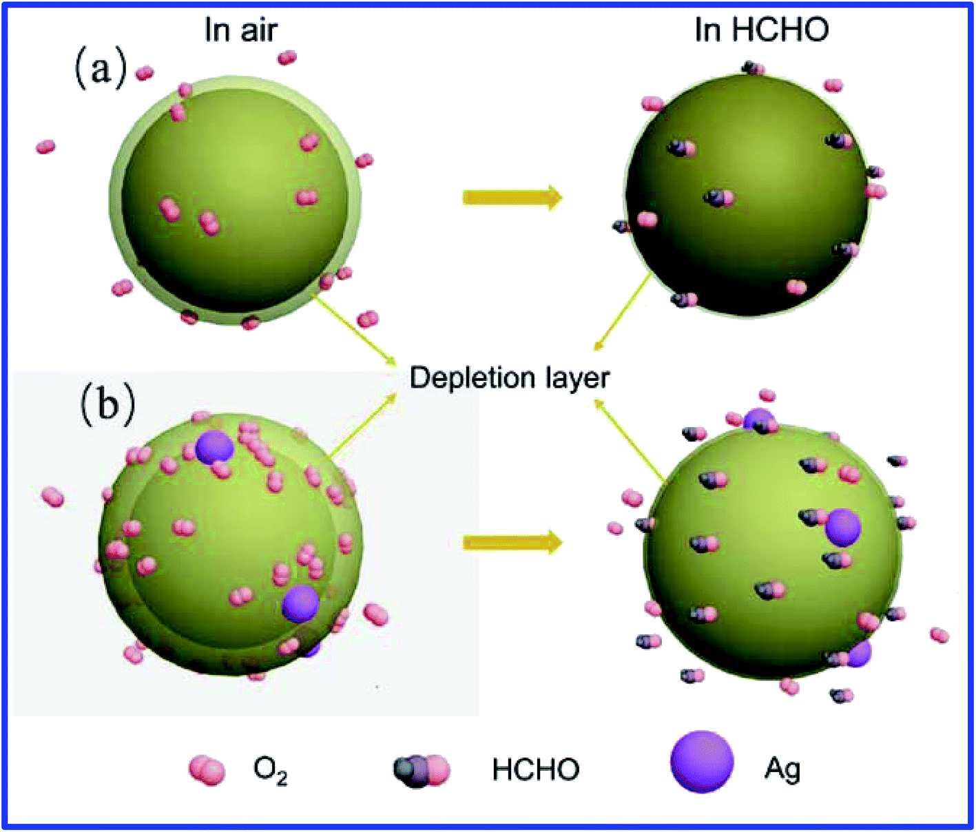 | ||
| Fig. 37 Schematic model of the depletion layer for SnO2/Sn3O4 materials when exposed to air and HCHO (a) before Ag decoration and (b) after Ag decoration,436 presented with permission and copyright. | ||
10. Comparison of Ga-doped ZnO and SnO2 as TCOs
Although this review article is focused on doped SnO2 for TCO applications, the reader should be aware that there are two other important categories of doped metal oxide TCOs, namely In2O3 and ZnO.116 The most commonly used TCO material, ITO, belongs to the former category. Although it is often referred to as Sn doped indium oxide, it is actually a mixed compound of In2O3 and SnO2 with the former being the dominant component. Given the limited global geological reserves of indium of ∼6000 tonnes,116 it is essential to develop alternative sustainable TCOs for optoelectronic as well as energy devices. Doped ZnO is a more recent and promising TCO material that offers a similar performance with respect to doped SnO2. Research on ZnO based TCO began during the 1990s. Since about 2010, the ZnO based TCO has been recognized as a viable low-cost alternative to ITO, especially for thin film photovoltaic devices. In this section, ZnO based TCOs will be briefly compared with those based on SnO2 to provide a more balanced perspective.ZnO is a wide bandgap semiconductor with a hexagonal wurtzite crystal structure and a direct energy bandgap of 3.28 eV.437 The ZnO band gap is wider than that of In2O3 (2.9 eV) but narrower than that of SnO2 (3.62 eV).116 The electron affinity of ZnO is 4.35 eV. Like SnO2, undoped ZnO is weakly n-type with a typical carrier (electron) concentration of ∼1017 cm−3. The carrier concentration and the electrical conductivity of ZnO can be increased by doping with a wide variety of n-type dopants such as: Ga, Al, B, In, Si, Ge, Ti and F.180 These dopants donate electrons to the conduction band of ZnO by substituting Zn2+ ions in the ZnO lattice. Amongst the above dopants, Ga and Al are the more widely studied and they are also commercially important.438 For brevity, we focus on TCO films based on Ga doped ZnO (GZO). There has been much interest in GZO as a viable alternative to ITO and doped SnO2 because GZO is a low cost, earth abundant material that is non-toxic and sustainable. Table 6, which has a structure similar to those of Tables 1 and 2, summarizes the deposition processes and properties of GZO films, as reported in the literature over the period 1997–2020.439–452 Similar to doped SnO2, GZO can be deposited by a variety of solution processing and physical vapor deposition techniques. The main solution processing techniques for GZO deposition are sol–gel spin coating and spray pyrolysis (or chemical spray).440,448,451,452 For physical vapor deposition of GZO, the main techniques used are RF magnetron sputtering,445,446,449,450 DC reactive sputtering,444 aerosol assisted CVD,439 ALD441 and PLD.442,443 Although not explicitly stated, the typical Ga dopant concentration used during deposition is in the range of 1–9 at% for the cited references in Table 6.439–452 The process temperature column refers to the highest processing temperature for the deposition techniques shown. It can be seen that for most of these techniques, deposition of GZO can be carried out by using mild to moderate substrate heating (40–400 °C) and room temperature deposition is possible for RF sputtering.449 This is especially important for the deposition of TCOs for thin film photovoltaic devices fabricated on flexible polymeric substrates or substrates with low melting points.
| Deposition technique | Process temperature (°C) | Thickness (nm) | Resistivity (Ω cm) | Average transmittance (%) | Mobility (cm2 V−1 s−1) | Reference |
|---|---|---|---|---|---|---|
| Spray pyrolysis | 350–500 | ∼350 | 4.9 × 10⁻² | 85 | — | Tiburcio-Silver et al.451 |
| RF sputtering | 100–300 | — | 2.2 × 10⁻⁴ | 85.9 | 10–30 | Miyazaki et al.450 |
| RF sputtering | RT | 600–800 | 7.8 × 10⁻⁴ | 80 | 14.1 | Gong et al.449 |
| Chemical spray | 425–525 | 600 | 7.4 × 10⁻³ | 80 | 0.1–1.0 | Gómez et al.448 |
| Sol–gel | 500 | 65 | 280 | 91/5 | — | Tsay et al.452 |
| Spray pyrolysis | 350 | 200 | 6.8 × 10⁻³ | ∼90 | 29.2 | Rao et al.447 |
| RF sputtering | 40–60 | 50–80 | 3.1 × 10⁻⁴ | 83 | 3–12 | Yu et al.446 |
| RF sputtering | RT | 600 | 2.6 × 10⁻⁴ | 90 | 1–10 | Assunção et al.445 |
| DC reactive sputtering | 300 | 500 | 3.51 × 10⁻⁴ | 90 | 4–8 | Ma et al.444 |
| PLD | 100–500 | 200 | 8.12 × 10⁻⁵ | 90 | 19.12–30.96 | Park et al.443 |
| PLD | RT to 500 | 200–300 | 5.96 × 10⁻⁴ | 92 | 0.1–10 | Vincze et al.442 |
| ALD | 200–300 | 60–70 | 4 × 10⁻⁴ | 95 | 6.4–20 | Szabó et al.441 |
| Sol–gel | 300–500 | — | 4.6 × 10⁻³ | — | 6.7–9.78 | Al-Asedy et al.440 |
| Aerosol assisted CVD | 450 | 400–600 | 7.8 × 10⁻⁴ | >80 | 7.7–15.1 | Ponja et al.439 |
The resistivity of GZO films shown in Table 6 is the minimum resistivity reported in each publication. These are generally within the range of 1 × 10⁻⁴ to 5 × 10⁻² Ω cm and are comparable to the resistivity of doped SnO2 tabulated in Tables 1 and 2. The low resistivity for GZO is partly due to a high carrier concentration in the range of 1020–1021 cm−3.8 The PLD technique in particular can yield the lowest GZO resistivity of 8.12 × 10⁻⁵ Ω cm, which is comparable to the lowest reported resistivity of ∼7.7 × 10⁻⁵ Ω cm for ITO.453 Note that both solution processing and physical vapor deposition techniques can yield GZO films with resistivity within this range of 1 × 10⁻⁴ to 5 × 10⁻² Ω cm, which is a narrower range than that of SnO2 in Tables 1 and 2.
As for optical properties, the average transmittance of GZO films in the visible range in Table 6 is consistent in the range of 80–90% for GZO deposited by solution processing and physical vapor deposition techniques. The average transmittance of GZO films is comparable to that of doped SnO2 films deposited by physical vapor deposition, as shown in Table 2. The Hall mobility of GZO films shown in Table 6 is generally in the range of 1–30 cm2 V−1 s−1. This is again comparable to the mobility of doped SnO2 films shown in Tables 1 and 2.
In addition to the properties shown in Table 6, GZO is known to be chemically stable at elevated temperatures,454 and the electrical resistivity of some doped ZnO is not a sensitive function of temperature.455 Both these properties are advantageous from a device fabrication standpoint. Surface morphology is another critically important property of TCOs because the surface roughness can cause pinholes in film layers deposited over the TCO. For GZO, it has been found that increasing the Ga dopant concentration in ZnO can enhance the surface diffusion and both the crystallite size and RMS surface roughness are reduced.456 A 1.17 nm RMS surface roughness has been observed for sol–gel derived GZO with 5 at% Ga.452 The comparison of materials data listed in Tables 1, 2 and 6 shows that GZO is an equally suitable TCO thin film material as doped SnO2. One known drawback of ZnO based TCO, however, is its vulnerability to damp heat.116 Under direct exposure to damp heat at 85 °C and high relative humidity of 85%, the film properties of Al doped ZnO (AZO) have been observed to deteriorate rapidly.116 For transparent flexible electronics, there may be an advantage in using GZO because ZnO is also an important transparent semiconducting oxide for the channel layer of thin film transistors (TFTs).457 A TFT is often used as the pixel switching device for the backplane circuit of active matrix displays and for flexible electronic circuits. This allows the same metal oxide material to be used for the channel and the substrate.
The present review emphasizes on enhancing the electrical and optical performances of SnO2 by designing suitable dopants, synthesis approaches via physical and chemical methods, formation of a multilayer structure with metals, and functionalization of the SnO2 layer. The high visible transmittance, electrical conductivity and bulk carrier mobility can be tuned precisely by selecting the dopants and synthesis process. Fig. 38a depicts the mapping of dopants to achieve high electrical conductivity, visible transmittance, electron mobility and thermal stability. It is also worth noting that the device performance significantly depends on the design of the dopants in SnO2 (Fig. 38b).
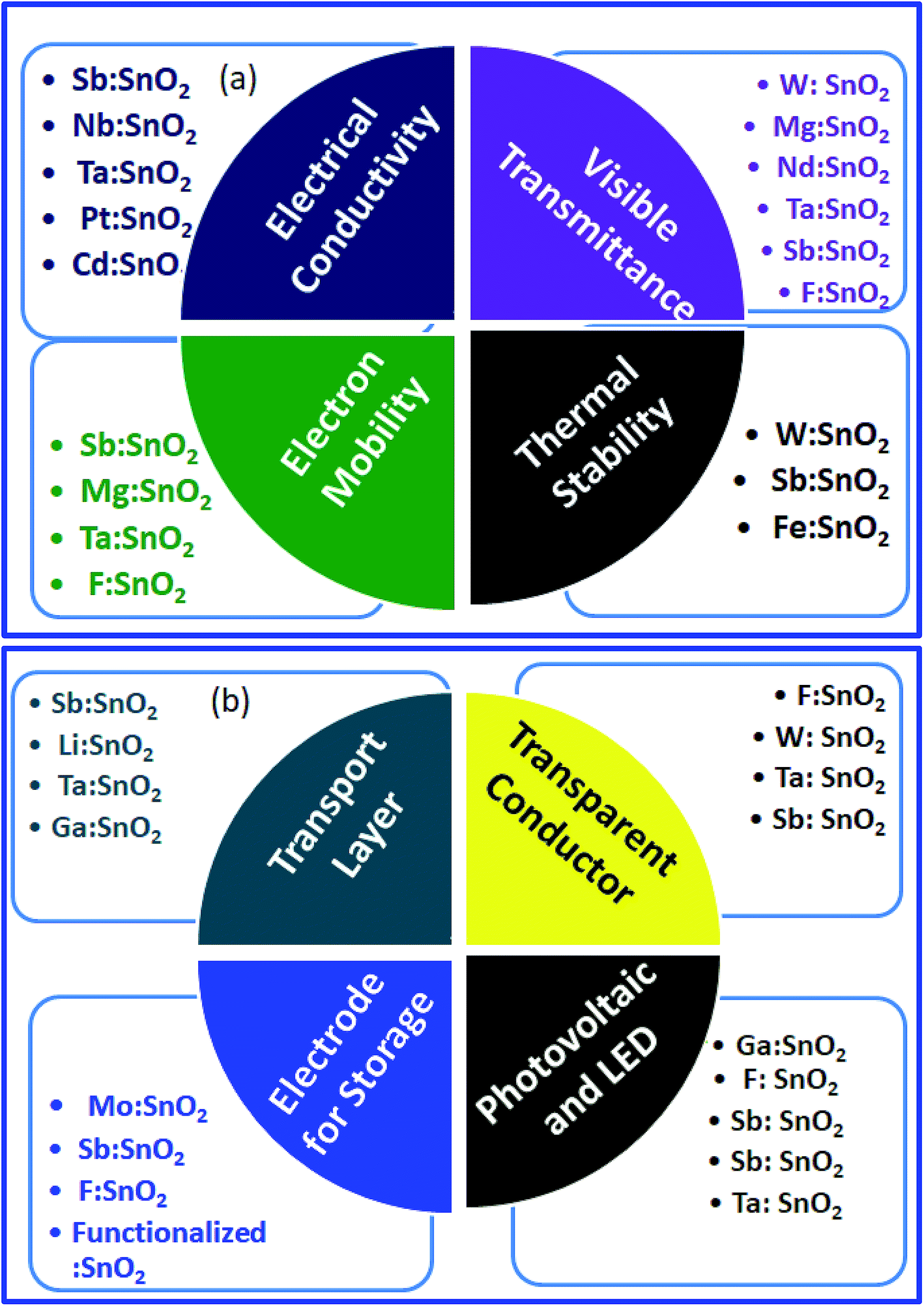 | ||
| Fig. 38 (a) Selection of dopants for high electrical conductivity, visible transmittance, carrier mobility and thermal stability. (b) Selection of dopants for different applications. | ||
The review has been designed from the perspective of basic information about SnO2 to the advance development of SnO2 through different processes, structuring, and dopant design. We have emphasized on the synthesis of SnO2 using the sol–gel method, spray coating, chemical bath deposition, sputter deposition technique and CVD at the industrial level, for large scale deployment of SnO2 based photovoltaic devices and energy storage devices. Furthermore, since SnO2 plays a critical role as the charge transport layer, this review maps the dopants of SnO2 for various applications (Fig. 39) and studied in detail the impact of a SnO2 based ETL for photovoltaic, LED, and wearable devices towards designing stable and efficient organic/inorganic and perovskite-based solar cells and LEDs.
 | ||
| Fig. 39 Doped SnO2 for various applications. | ||
11. Conclusions and future perspectives
Doped SnO2 is a promising non-toxic earth-abundant TCO that can be synthesized by using both solution and vacuum-based deposition techniques. Different types of cationic and anionic dopants such as Sb, Nb, Co, Ga, Al, Ta, W, F, Li, Mo, and N have been discussed in detail. The substitution of Sn4+ or O2− ions by these dopant elements modifies the electronic structure of SnO2 and results in changes of material properties. Sb and F are the most suitable dopants for SnO2 because both ATO and FTO can simultaneously achieve desired properties in transparency, resistivity, mechanical hardness, environmental stability, and Hall mobility. In the case of NBO, the radii of Nb and Sn are closer than that of F, resulting in higher conductivity than FTO. Ga-doped SnO2 is an efficient electron transport material in planar perovskite solar cells. In addition, Al- and-Ga doped tin oxide can convert the conductivity type from n-type (pure SnO2) to p-type. Ta-doped SnO2 epitaxial films show excellent Hall mobility of ∼58 cm2 V−1 s−1 and transparency extended to the UV-B spectral region (280–315 nm), which enables applications in transparent electric and photoelectric devices.Apart from dopant categories, the surface roughness, film thickness and thermal treatment have significant impacts on the electrical and optical properties of optoelectronics devices. Smoother surfaces reduce the contact resistance and localized field effects. On the other hand, intentionally designed rough or patterned surfaces trap incident light through increasing the optical path length of the light, thereby increasing the amount of light absorbed by the active layers. A pyramidal surface is found to have a larger transmission and efficiency than a planar surface.
The structural, optical, and electronic properties of doped SnO2 significantly depend on the growth procedure and postdeposition thermal treatment. Furthermore, the temperature gradient from the surface of the film to the substrate can limit impurity diffusion from the substrate. For the SnO2/metal based multilayer thin films, which also show high conductivity and visible transmittance, a grid structure fabricated by the lift-off process can further enhance the visible transmittance without adversely affecting the electrical properties of the multilayer.
Thin-film SnO2 can also act as an ETL on FTO substrates. Doped SnO2 can enhance the performance of OLED and photovoltaic devices by facilitating the electron injection and extraction, respectively, through improved alignment of the conduction band edge with the metal Fermi level. For perovskite thin film solar cells, annealing the SnO2 ETL in the range of 100 °C to 300 °C can reduce the hysteresis of the current–voltage characteristics under illumination. Plasma treatment of SnO2 has significant positive impact on the photovoltaic device performance. Ozone-treated SnOx was found to be the best hole blocking layer and an ITO-free semitransparent bottom electrode based on the SnOx/Ag/SnOx architecture has been designed. The low temperature and atmospheric pressure plasma process can be useful for the large-scale roll-to-roll functionalization of SnO2 for different applications. An emerging application of doped SnO2 is in the field of electrical energy storage devices. SnO2 has been used as a component of the composite material for the anode of LIBs and as an adsorption layer for the cathode of Li–S batteries.
The increasing demand for optoelectronics, photovoltaics and energy storage devices requires the development of cost-effective but at the same time high-performance TCOs and ETLs in terms of conductivity and transparency. The low cost, non-toxic nature, high specific capacity, high transparency in the visible range and high electron mobility properties have made tin oxide a potential material for these applications. Understanding and controlling their structure, chemical properties, surface functionalization, surface roughness and film thickness are the key to optimize the performance of the SnO2 based structures. Great contributions have been made to date, like doping SnO2 with suitable materials through several synthesis processes, functionalization of SnO2 through plasma treatment and energy band alignment through band engineering.
However, looking toward the future, there are still some challenges to overcome for the use of SnO2 in industrial applications. The use of a dopant to increase the electrical conductivity needs further screening and investigation to find the most advantageous dopant and deposition technique. A two-step sputtering method can be used to improve the crystal quality of the SnO2 without causing interface damage at the oxide/substrate interface. Thermal stability is still a critical issue for the SnO2 based devices. By designing the suitable passivation on the substrates, it is possible to avoid the interface damage and interdiffusion of elements during thermal treatment. Therefore, oxide/SnO2 bilayer design will play a key role in suppressing the bulk defects and recombination centers. More work is needed to achieve a precise control of composition, film quality, defects, crystallinity, and dopant activation, which will improve the conversion efficiency and stability of the device. It is important to simplify the fabrication process and use techniques like solution and plasma-based technologies for large scale and roll-to-roll deposition and sustainable production. Doped SnO2 has a huge potential for energy saving, and transparent smart window applications. However, there is a lack of investigation about the SnO2 based heat reflecting coating. Furthermore, SnO2 based cool paint can be a game changer for the super-low-energy buildings. A focused investigation on solution based doped SnO2 is required to achieve the SnO2 based cool paint to reduce the energy consumption for indoor thermal comfort.
Though a lot of work has been done, there is still a long way to go for commercializing SnO2 in the field of energy storage devices. As discussed in Section 8.1, SnO2 can be a crucial component in modifying the cathode, anode and separator in traditional LIBs. However, the specific charge capacity, specific power and cyclability all need to be improved and should be the focus of research in the near future. The synthesis of novel nanostructured SnO2 composite materials with high porosity and high specific area for supercapacitor electrodes is another important topic worthy of further investigation. The main problem associated with Li–S batteries (which is considered as the next big thing in the energy storage field) is polysulfide shuttling and growth of Li dendrites. From our discussion, we have seen that these problems associated with Li–S batteries can be addressed by utilizing SnO2 nanoparticles. For supercapacitors, the contemporary metal oxides like NiO, MnO2, and Co3O4 are more favourable as supercapacitor electrodes as compared to SnO2. However, these oxides also have their disadvantages, and if the electrochemical properties of SnO2 can be tuned by controlling the morphology, or by a doping strategy or by coupling with MXenes, CNTs and conducting polymers, there is a possibility of a commercial supercapacitor prototype using the SnO2 electrode material.
The current trend of using tin oxide materials for optoelectronic and energy storage devices is a challenge that involves materials scientists and mechanical, electrical and chemical engineers. It should be recognized that doped SnO2 and doped ZnO (e.g. GZO) are complementary TCOs. In terms of materials properties, sustainability and cost, these two oxide categories are comparable and offer the materials community two good alternatives. Nevertheless, this comprehensive review article will provide key guidelines for the materials synthesis and the mapping of SnO2 based TCOs, ETLs, and electrodes for performance-improving strategies towards accentuating the device performance.
Author contributions
GKD/PS/SK/MS/AKC: concept/design and drafting; HS and PB: investigation (electrical properties, original draft); AG and SM: formal analysis and original draft (perovskite and transport layer); NC and AKC: formal analysis, energy storage devices (LSB, supercapacitors, electrochromics), abstract and introduction; QL, GS, and PS: investigation, formal analysis, original draft and supervision (organic and ETL, LIBS); AK, SC, and SB: synthesis, thermal treatment, and electronic properties; AD, CSR and SK: funding acquisition, formal analysis, plasma treatment, thermal treatment and future prospect; TW: abstract, perovskite, and transparent PV, summary and outlook; SZ and SG: physical vapor deposition; CM: original draft (morphology study); Avishek Kumar: electronic properties and solution method; and SR: original draft (physical and solution methods). All authors equally commented on and edited the manuscript.Conflicts of interest
There are no conflicts to declare.Acknowledgements
GKD is thankful to the National University of Singapore, Global Challenges Research Fund, The Open University UK, and Ming-Chi University of Technology-Taiwan for providing funding support to visiting faculty. Sajal Biring acknowledges the financial assistance from the Ministry of Science and Technology, Taiwan (MOST 109-2221-E-131-002). P. S. is thankful to QUT for financial support, the Australian Research Council (ARC) for the Future Fellowship (FT130101337), QUT core funding (QUT/322120-0301/07) and Centre for Materials Science, QUT for their generous support. NC and AKC acknowledge the MHRD, Govt. of India for funding under TEQIP-III (CoE), May 2018. SK acknowledges Recycling Lithium ion batteries for a sustainable technological and economic development (ReListed) DSTUKIERI-2018-19-008, Royal Society IES\R2\170272 Royal Academy of Engineering Newton Fund and European Commission Smart innovative system for recycling wastewater project id: 958491 and creating closed loops in textile manufacturing industrial processes, and Global Challenges Research Fund on cleaning systems for solar cells.References
- R. A. Maniyara, V. K. Mkhitaryan, T. L. Chen, D. S. Ghosh and V. Pruneri, Nat. Commun., 2016, 7, 13771 CrossRef CAS PubMed.
- G. K. Dalapati, A. K. Kushwaha, M. Sharma, V. Suresh, S. Shannigrahi, S. Zhuk and S. Masudy-Panah, Prog. Mater. Sci., 2018, 95, 42–131 CrossRef CAS.
- S. D. Ponja, B. A. D. Williamson, S. Sathasivam, D. O. Scanlon, I. P. Parkin and C. J. Carmalt, J. Mater. Chem. C, 2018, 6, 7257–7266 RSC.
- L. Mai, D. Zanders, E. Subaşı, E. Ciftyurek, C. Hoppe, D. Rogalla, W. Gilbert, T. d. l. Arcos, K. Schierbaum, G. Grundmeier, C. Bock and A. Devi, ACS Appl. Mater. Interfaces, 2019, 11, 3169–3180 CrossRef CAS PubMed.
- M. J. Powell, B. A. D. Williamson, S.-Y. Baek, J. Manzi, D. B. Potter, D. O. Scanlon and C. J. Carmalt, Chem. Sci., 2018, 9, 7968–7980 RSC.
- D. Mohanta and M. Ahmaruzzaman, RSC Adv., 2016, 6, 110996–111015 RSC.
- Y. Zhang, C. Ma, X. Lu and M. Liu, Mater. Horiz., 2019, 6, 911–930 RSC.
- V. Ganesh, M. Arif, M. A. Manthrammel, M. Shkir, A. Singh and S. AlFaify, Opt. Mater., 2019, 94, 277–285 CrossRef CAS.
- K. Ellmer, Nat. Photonics, 2012, 6, 809–817 CrossRef CAS.
- C.-Y. Kim and D.-H. Riu, Thin Solid Films, 2011, 519, 3081–3085 CrossRef CAS.
- S. Yu, L. Li, X. Lyu and W. Zhang, Sci. Rep., 2016, 6, 20399 CrossRef CAS PubMed.
- S. C. Dixon, D. O. Scanlon, C. J. Carmalt and I. P. Parkin, J. Mater. Chem. C, 2016, 4, 6946–6961 RSC.
- J. Barbé, M. L. Tietze, M. Neophytou, B. Murali, E. Alarousu, A. E. Labban, M. Abulikemu, W. Yue, O. F. Mohammed, I. McCulloch, A. Amassian and S. Del Gobbo, ACS Appl. Mater. Interfaces, 2017, 9, 11828–11836 CrossRef PubMed.
- D. Slocombe, A. Porch, M. Pepper and P. P. Edwards, Energy Environ. Sci., 2012, 5, 5387–5391 RSC.
- R. R. Kasar, N. Deshpande, Y. Gudage, J. Vyas and R. Sharma, Phys. B, 2008, 403, 3724–3729 CrossRef CAS.
- M. J. Mortelliti, A. N. Wang and J. L. Dempsey, Polyhedron, 2019, 171, 433–447 CrossRef CAS.
- C. G. Granqvist, Sol. Energy Mater. Sol. Cells, 2007, 91, 1529–1598 CrossRef CAS.
- J. Sawahata and T. Kawasaki, Thin Solid Films, 2019, 685, 210–215 CrossRef CAS.
- H. B. Lee, W.-Y. Jin, M. M. Ovhal, N. Kumar and J.-W. Kang, J. Mater. Chem. C, 2019, 7, 1087–1110 RSC.
- K. Sakamoto, H. Kuwae, N. Kobayashi, A. Nobori, S. Shoji and J. Mizuno, Sci. Rep., 2018, 8, 2825 CrossRef PubMed.
- S. Ke, C. Chen, N. Fu, H. Zhou, M. Ye, P. Lin, W. Yuan, X. Zeng, L. Chen and H. Huang, ACS Appl. Mater. Interfaces, 2016, 8, 28406–28411 CrossRef CAS PubMed.
- J. E. N. Swallow, B. A. D. Williamson, T. J. Whittles, M. Birkett, T. J. Featherstone, N. Peng, A. Abbott, M. Farnworth, K. J. Cheetham, P. Warren, D. O. Scanlon, V. R. Dhanak and T. D. Veal, Adv. Funct. Mater., 2018, 28, 1701900 CrossRef.
- C. Guillén and J. Herrero, Thin Solid Films, 2011, 520, 1–17 CrossRef.
- B.-j. Li, L.-j. Huang, M. Zhou, N.-f. Ren and B. Wu, Ceram. Int., 2014, 40, 1627–1633 CrossRef CAS.
- N. Noor, C. K. T. Chew, D. S. Bhachu, M. R. Waugh, C. J. Carmalt and I. P. Parkin, J. Mater. Chem. C, 2015, 3, 9359–9368 RSC.
- Y. Zhang, H. Zhang, J. Zhang, J. Wang and Z. Li, RSC Adv., 2015, 5, 106258–106264 RSC.
- C.-Y. Tsay and S.-C. Liang, J. Alloys Compd., 2015, 622, 644–650 CrossRef CAS.
- D. Langley, G. Giusti, C. Mayousse, C. Celle, D. Bellet and J.-P. Simonato, Nanotechnology, 2013, 24, 452001 CrossRef PubMed.
- W. Zhou, R. Liu, Q. Wan, Q. Zhang, A. L. Pan, L. Guo and B. Zou, J. Phys. Chem. C, 2009, 113, 1719–1726 CrossRef CAS.
- R. Yang, Y. Gu, Y. Li, J. Zheng and X. Li, Acta Mater., 2010, 58, 866–874 CrossRef CAS.
- M. Kam, Q. Zhang, D. Zhang and Z. Fan, Sci. Rep., 2019, 9, 6963 CrossRef PubMed.
- Y. Cong, D. Han, J. Dong, S. Zhang, X. Zhang and Y. Wang, Sci. Rep., 2017, 7, 1497 CrossRef PubMed.
- N. Chakrabarty, M. Char, S. Krishnamurthy and A. K. Chakraborty, Mater. Adv., 2021, 2, 366–375 RSC.
- P. Chatterjee and A. K. Chakraborty, Opt. Mater., 2021, 111, 110610 CrossRef CAS.
- S. M. D. Watson, K. S. Coleman and A. K. Chakraborty, ACS Nano, 2008, 2, 643–650 CrossRef CAS PubMed.
- N. Chakrabarty, A. Dey, S. Krishnamurthy and A. K. Chakraborty, Appl. Surf. Sci., 2021, 536, 147960 CrossRef CAS.
- P. Tiwary, R. Mahapatra and A. K. Chakraborty, J. Mater. Sci.: Mater. Electron., 2019, 30, 5464–5469 CrossRef CAS.
- S. Gupta Chatterjee, S. Dey, D. Samanta, S. Santra, S. Chatterjee, P. K. Guha and A. K. Chakraborty, J. Mater. Sci.: Mater. Electron., 2018, 29, 20162–20171 CrossRef CAS.
- S.-W. Lee, K.-J. Choi, B.-H. Kang, J.-S. Lee, S.-W. Kim, J.-B. Kwon, S.-A. Gopalan, J.-H. Bae, E.-S. Kim, D.-H. Kwon and S.-W. Kang, Org. Electron., 2016, 39, 250–257 CrossRef CAS.
- K.-S. Cho and H.-K. Kim, RSC Adv., 2018, 8, 2599–2609 RSC.
- C. Hudaya, B. J. Jeon and J. K. Lee, ACS Appl. Mater. Interfaces, 2015, 7, 57–61 CrossRef CAS PubMed.
- J. J. Lee, J.-Y. Ha, W.-K. Choi, Y. S. Cho and J.-W. Choi, ACS Comb. Sci., 2015, 17, 247–252 CrossRef CAS PubMed.
- A. Stadler, Materials, 2012, 5, 661–683 CrossRef PubMed.
- T. Minami, Thin Solid Films, 2008, 516, 1314–1321 CrossRef CAS.
- Z. Ghorannevis, E. Akbarnejad and M. Ghoranneviss, J. Theor. Appl. Phys., 2015, 9, 285–290 CrossRef.
- Q. Wan, E. N. Dattoli, W. Y. Fung, W. Guo, Y. Chen, X. Pan and W. Lu, Nano Lett., 2006, 6, 2909–2915 CrossRef CAS PubMed.
- L. Passoni, F. Fumagalli, A. Perego, S. Bellani, P. Mazzolini and F. Di Fonzo, Nanotechnology, 2017, 28, 245603 CrossRef PubMed.
- B. Yang, C. Yao, Y. Yu, Z. Li and X. Wang, Sci. Rep., 2017, 7, 4936 CrossRef PubMed.
- K. Higashitani, C. E. McNamee and M. Nakayama, Langmuir, 2011, 27, 2080–2083 CrossRef CAS PubMed.
- S. Das and V. Jayaraman, Prog. Surf. Sci., 2014, 66, 112–255 CAS.
- K. Jenifer, S. Arulkumar, S. Parthiban and J. Y. Kwon, J. Electron. Mater., 2020, 49, 7098–7111 CrossRef.
- A. M. Al-Hamdi, U. Rinner and M. Sillanpää, Process Saf. Environ. Prot., 2017, 107, 190–205 CrossRef CAS.
- Q. Jiang, X. Zhang and J. You, Small, 2018, 14, 1801154 CrossRef PubMed.
- A. M. Ganose and D. O. Scanlon, J. Mater. Chem. C, 2016, 4, 1467–1475 RSC.
- M. Park, K. Jae-Yup, H. Son, C.-H. Lee, S. Jang and M. Ko, Nano Energy, 2016, 26, 208–215 CrossRef CAS.
- Y. Bai, Y. Fang, Y. Deng, Q. Wang, J. Zhao, X. Zheng, Y. Zhang and J. Huang, ChemSusChem, 2016, 9, 2686–2691 CrossRef CAS PubMed.
- L. Xiong, Y. Guo, J. Wen, H. Liu, G. Yang, P. Qin and G. Fang, Adv. Funct. Mater., 2018, 28, 1802757 CrossRef.
- Y. Chen, Q. Meng, L. Zhang, C. Han, H. Gao, Y. Zhang and H. Yan, J. Energy Chem., 2019, 35, 144–167 CrossRef.
- S. H. Saeedabad, G. S. Selopal, S. M. Rozati, Y. Tavakoli and G. Sberveglieri, J. Electron. Mater., 2018, 47, 5165–5173 CrossRef CAS.
- R. Milan, G. S. Selopal, M. Epifani, M. M. Natile, G. Sberveglieri, A. Vomiero and I. Concina, Sci. Rep., 2015, 5, 14523 CrossRef CAS PubMed.
- R. Milan, G. Singh Selopal, M. Cavazzini, S. Orlandi, R. Boaretto, S. Caramori, I. Concina and G. Pozzi, Sci. Rep., 2020, 10, 1176 CrossRef CAS PubMed.
- K. Basu, G. S. Selopal, M. Mohammadnezad, R. Akilimali, Z. M. Wang, H. Zhao, F. Vetrone and F. Rosei, Electrochim. Acta, 2020, 349, 136409 CrossRef CAS.
- Q. Dong, J. Li, Y. Shi, M. Chen, L. K. Ono, K. Zhou, C. Zhang, Y. Qi, Y. Zhou, N. P. Padture and L. Wang, Adv. Energy Mater., 2019, 9, 1900834 CrossRef.
- P. Shen, M. Yao, G. Wang, R. Mi, W. Guo, Y. Bai and L. Shen, J. Mater. Chem. A, 2018, 6, 17401–17408 RSC.
- D. Yang, R. Yang, K. Wang, C. Wu, X. Zhu, J. Feng, X. Ren, G. Fang, S. Priya and S. Liu, Nat. Commun., 2018, 9, 3239 CrossRef PubMed.
- S. Castro-Hermosa, G. Lucarelli, M. Top, M. Fahland, J. Fahlteich and T. M. Brown, Cell Rep. Phys. Sci., 2020, 1, 100045 CrossRef.
- M. Park, J. Roh, J. Lim, H. Lee and D. Lee, Nanomaterials, 2020, 10, 726 CrossRef CAS PubMed.
- Y. Liu, S. Wei, G. Wang, J. Tong, J. Li and D. Pan, Langmuir, 2020, 36, 6605–6609 CrossRef CAS PubMed.
- Y. Deng, C. Fang and G. Chen, J. Power Sources, 2016, 304, 81–101 CrossRef CAS.
- K. C. Mishra, K. H. Johnson and P. C. Schmidt, Phys. Rev. B: Condens. Matter Mater. Phys., 1995, 51, 13972–13976 CrossRef CAS PubMed.
- M. Batzill and U. Diebold, Prog. Surf. Sci., 2005, 79, 47–154 CrossRef CAS.
- Ç. Kılıç and A. Zunger, Phys. Rev. Lett., 2002, 88, 095501 CrossRef PubMed.
- K. B. Sundaram and G. K. Bhagavat, J. Phys. D: Appl. Phys., 1981, 14, 921–925 CrossRef CAS.
- C. Ke, W. Zhu, Z. Zhang, E. Soon Tok, B. Ling and J. Pan, Sci. Rep., 2015, 5, 17424 CrossRef CAS PubMed.
- Y. W. Noh, J. H. Lee, I. S. Jin, S. H. Park and J. W. Jung, Nano Energy, 2019, 65, 104014 CrossRef CAS.
- L. Xiong, M. Qin, G. Yang, Y. Guo, H. Lei, Q. Liu, W. Ke, H. Tao, P. Qin, S. Li, H. Yu and G. Fang, J. Mater. Chem. A, 2016, 4, 8374–8383 RSC.
- D. Wang, S.-C. Chen and Q. Zheng, J. Mater. Chem. C, 2019, 7, 12204–12210 RSC.
- J. Song, W. Zhang, D. Wang, K. Deng, J. Wu and Z. Lan, Sol. Energy, 2019, 185, 508–515 CrossRef CAS.
- H. Ye, Z. Liu, X. Liu, B. Sun, X. Tan, Y. Tu, T. Shi, Z. Tang and G. Liao, Appl. Surf. Sci., 2019, 478, 417–425 CrossRef CAS.
- Z. Xu, S. H. Teo, L. Gao, Z. Guo, Y. Kamata, S. Hayase and T. Ma, Org. Electron., 2019, 73, 62–68 CrossRef CAS.
- Z. Ma, W. Zhou, Z. Xiao, H. Zhang, Z. Li, J. Zhuang, C. Peng and Y. Huang, Org. Electron., 2019, 71, 98–105 CrossRef CAS.
- R. Ramarajan, N. Purushothamreddy, R. K. Dileep, M. Kovendhan, G. Veerappan, K. Thangaraju and D. Paul Joseph, Sol. Energy, 2020, 211, 547–559 CrossRef CAS.
- O. S. Elsherif, G. E. A. Muftah, O. Abubaker and I. M. Dharmadasa, J. Mater. Sci.: Mater. Electron., 2016, 27, 12280–12286 CrossRef CAS.
- A. Way, J. Luke, A. D. Evans, Z. Li, J.-S. Kim, J. R. Durrant, H. K. H. Lee and W. C. Tsoi, AIP Adv., 2019, 9, 085220 CrossRef.
- S. Das and V. Jayaraman, Prog. Mater. Sci., 2014, 66, 112–255 CrossRef CAS.
- B. Bissig, T. Jäger, L. Ding, A. N. Tiwari and Y. E. Romanyuk, APL Mater., 2015, 3, 062802 CrossRef.
- E. Elangovan and K. Ramamurthi, Thin Solid Films, 2005, 476, 231–236 CrossRef CAS.
- S. Gürakar, T. Serin and N. Serin, Appl. Surf. Sci., 2015, 352, 16–22 CrossRef.
- Z. Y. K. Banyamin, P. J. Kelly, G. West and J. Boardman, Coatings, 2014, 4, 732–746 CrossRef.
- Ç. Kılıç and A. Zunger, Phys. Rev. Lett., 2002, 88, 095501 CrossRef PubMed.
- V. Sharma, R. Vyas, P. Bazylewski, G. S. Chang, K. Asokan and K. Sachdev, RSC Adv., 2016, 6, 29135–29141 RSC.
- J. Heo, A. S. Hock and R. G. Gordon, Chem. Mater., 2010, 22, 4964–4973 CrossRef CAS.
- M. A. Hossain, J. R. Jennings, Z. Y. Koh and Q. Wang, ACS Nano, 2011, 5, 3172–3181 CrossRef CAS PubMed.
- J. Liu, T. Luo, T. S. Mouli, F. Meng, B. Sun, M. Li and J. Liu, Chem. Commun., 2010, 46, 472–474 RSC.
- F. Gyger, M. Hübner, C. Feldmann, N. Barsan and U. Weimar, Chem. Mater., 2010, 22, 4821–4827 CrossRef CAS.
- S. Kang, R. Nandi, J.-K. Sim, J.-Y. Jo, U. Chatterjee and C.-R. Lee, RSC Adv., 2017, 7, 48113–48119 RSC.
- M. Esro, S. Georgakopoulos, H. Lu, G. Vourlias, A. Krier, W. I. Milne, W. P. Gillin and G. Adamopoulos, J. Mater. Chem. C, 2016, 4, 3563–3570 RSC.
- X. Yu, T. J. Marks and A. Facchetti, Nat. Mater., 2016, 15, 383–396 CrossRef CAS PubMed.
- X. Huang, J. Du, X. Guo, Z. Lin, J. Ma, J. Su, L. Feng, C. Zhang, J. Zhang, J. Chang and Y. Hao, Sol. RRL, 2020, 4, 1900336 CrossRef CAS.
- D. Cheng, M. Zhang, J. Chen, C. Yang, X. Zeng and D. Cao, J. Phys. Chem. C, 2014, 118, 2037–2043 CrossRef CAS.
- S. Yu, W. Zhang, L. Li, D. Xu, H. Dong and Y. Jin, Appl. Surf. Sci., 2013, 286, 417–420 CrossRef CAS.
- W. Yang, S. Yu, Y. Zhang and W. Zhang, Thin Solid Films, 2013, 542, 285–288 CrossRef CAS.
- B.-j. Li, L.-j. Huang, N.-f. Ren, X. Kong, Y.-l. Cai and J.-l. Zhang, Appl. Surf. Sci., 2015, 351, 113–118 CrossRef CAS.
- A. H. Omran Alkhayatt and S. K. Hussian, Mater. Lett., 2015, 155, 109–113 CrossRef CAS.
- K. Anandan and V. Rajendran, Superlattices Microstruct., 2015, 85, 185–197 CrossRef CAS.
- G. Turgut, Thin Solid Films, 2015, 594, 56–66 CrossRef CAS.
- S. Nakao, N. Yamada, T. Hitosugi, Y. Hirose, T. Shimada and T. Hasegawa, Thin Solid Films, 2010, 518, 3093–3096 CrossRef CAS.
- S.-H. Cho, R. Pandey, C.-H. Wie, Y. J. Lee, J.-W. Lim, D.-H. Park, J.-S. Seok, Y.-H. Jang, K.-K. Kim, D. K. Hwang, D.-J. Byun and W.-K. Choi, Phys. Status Solidi B, 2014, 211, 1860–1867 CrossRef CAS.
- L. Soussi, T. Garmim, O. Karzazi, A. Rmili, A. El Bachiri, A. Louardi and H. Erguig, Surf. Interfaces, 2020, 19, 100467 CrossRef CAS.
- S. Sambasivam, P. S. Maram, C. V. V. Muralee Gopi and I. M. Obaidat, Optik, 2020, 202, 163596 CrossRef CAS.
- L. Zhang, W. Xu, W. Liu, P. Cao, S. Han, D. Zhu and Y. Lu, J. Phys. D: Appl. Phys., 2020, 53, 175106 CrossRef CAS.
- Q. Chen and E. Thimsen, ACS Appl. Mater. Interfaces, 2020, 12, 25168–25177 CrossRef CAS PubMed.
- J. Ni, X. Zhao, X. Zheng, J. Zhao and B. Liu, Acta Mater., 2009, 57, 278–285 CrossRef CAS.
- J. Ni, X. Zhao and J. Zhao, J. Inorg. Organomet. Polym. Mater., 2012, 22, 21–26 CrossRef CAS.
- F. Fang, Y. Zhang, X. Wu, Q. Shao and Z. Xie, Mater. Res. Bull., 2015, 68, 240–244 CrossRef CAS.
- H. Liu, V. Avrutin, N. Izyumskaya, Ü. Özgür and H. Morkoç, Superlattices Microstruct., 2010, 48, 458–484 CrossRef CAS.
- G. Turgut, E. F. Keskenler, S. Aydın, E. Sönmez, S. Doğan, B. Düzgün and M. Ertuğrul, Superlattices Microstruct., 2013, 56, 107–116 CrossRef CAS.
- L. Wang, J. Yu, X. Niu, L. Wang, C. Fu, R. Qiu, W. Yan, H. Zhao and J. Yang, Thin Solid Films, 2018, 649, 147–153 CrossRef CAS.
- X. Huo, S. Jiang, P. Liu, M. Shen, S. Qiu and M.-Y. Li, CrystEngComm, 2017, 19, 4413–4423 RSC.
- Y. J. Wu, Y. S. Liu, C. Y. Hsieh, P. M. Lee, Y. S. Wei, C. H. Liao and C. Y. Liu, Appl. Surf. Sci., 2015, 328, 262–268 CrossRef CAS.
- T. Entradas, J. F. Cabrita, S. Dalui, M. R. Nunes, O. C. Monteiro and A. J. Silvestre, Mater. Chem. Phys., 2014, 147, 563–571 CrossRef CAS.
- C. E. Benouis, M. Benhaliliba, Z. Mouffak, A. Avila-Garcia, A. Tiburcio-Silver, M. Ortega Lopez, R. Romano Trujillo and Y. S. Ocak, J. Alloys Compd., 2014, 603, 213–223 CrossRef CAS.
- S. K. Sinha, S. K. Ray and I. Manna, Philos. Mag., 2014, 94, 3507–3521 CrossRef CAS.
- J. Zhao, X. J. Zhao, J. M. Ni and H. Z. Tao, Acta Mater., 2010, 58, 6243–6248 CrossRef CAS.
- S. Wang, L. Shi, G. Chen, C. Ba, Z. Wang, J. Zhu, Y. Zhao, M. Zhang and S. Yuan, ACS Appl. Mater. Interfaces, 2017, 9, 17163–17171 CrossRef CAS PubMed.
- G. Zhang, X. Zhang, H. Ning, H. Chen, Q. Wu, M. Jiang, C. Li, D. Guo, Y. Wang, R. Yao and J. Peng, Superlattices Microstruct., 2019, 130, 277–284 CrossRef CAS.
- M. S. Bannur, A. Antony, K. I. Maddani, A. Ani, P. Poornesh, A. Rao, K. S. Choudhari and S. D. Kulkarni, Opt. Mater., 2019, 94, 294–298 CrossRef CAS.
- L. He, C. Luan, X. Feng, H. Xiao, X. Yang, D. Wang and J. Ma, Ceram. Int., 2019, 45, 10196–10202 CrossRef CAS.
- F. Lungwitz, R. Escobar-Galindo, D. Janke, E. Schumann, R. Wenisch, S. Gemming and M. Krause, Sol. Energy Mater. Sol. Cells, 2019, 196, 84–93 CrossRef CAS.
- Z. Zhang, C. Yin, L. Yang, J. Jiang and Y. Guo, J. Alloys Compd., 2019, 785, 819–825 CrossRef CAS.
- G. Brunin, F. Ricci, V.-A. Ha, G.-M. Rignanese and G. Hautier, npj Comput. Mater., 2019, 5, 63 CrossRef.
- H. Peng, A. Zakutayev, S. Lany, T. R. Paudel, M. d'Avezac, P. F. Ndione, J. D. Perkins, D. S. Ginley, A. R. Nagaraja, N. H. Perry, T. O. Mason and A. Zunger, Adv. Funct. Mater., 2013, 23, 5267–5276 CrossRef CAS.
- G. Hautier, A. Miglio, G. Ceder, G.-M. Rignanese and X. Gonze, Nat. Commun., 2013, 4, 2292 CrossRef PubMed.
- F. Borgatti, J. A. Berger, D. Céolin, J. S. Zhou, J. J. Kas, M. Guzzo, C. F. McConville, F. Offi, G. Panaccione, A. Regoutz, D. J. Payne, J.-P. Rueff, O. Bierwagen, M. E. White, J. S. Speck, M. Gatti and R. G. Egdell, Phys. Rev. B, 2018, 97, 155102 CrossRef CAS.
- M. Kim, N. Marom, N. S. Bobbitt and J. R. Chelikowsky, J. Chem. Phys., 2015, 142, 044704 CrossRef PubMed.
- Z. Chen, Q. Xie, J. Ding, Z. Yang, W. Zhang and H. Cheng, ACS Appl. Mater. Interfaces, 2020, 12, 29937–29945 CAS.
- B. A. D. Williamson, T. J. Featherstone, S. S. Sathasivam, J. E. N. Swallow, H. Shiel, L. A. H. Jones, M. J. Smiles, A. Regoutz, T.-L. Lee, X. Xia, C. Blackman, P. K. Thakur, C. J. Carmalt, I. P. Parkin, T. D. Veal and D. O. Scanlon, Chem. Mater., 2020, 32, 1964–1973 CrossRef CAS PubMed.
- F. E. Ghodsi and J. Mazloom, Appl. Phys. A: Mater. Sci. Process., 2012, 108, 693–700 CrossRef CAS.
- R. M. Pasquarelli, D. S. Ginley and R. O'Hayre, Chem. Soc. Rev., 2011, 40, 5406–5441 RSC.
- H.-R. An, C. Kim, S.-T. Oh and H.-J. Ahn, Ceram. Int., 2014, 40, 385–391 CrossRef CAS.
- K. Bouras, G. Schmerber, D. Aureau, H. Rinnert, J.-L. Rehspringer, D. Ihiawakrim, A. Dinia, A. Slaoui and S. Colis, Phys. Chem. Chem. Phys., 2019, 21, 21407–21417 RSC.
- A. E. Danks, S. R. Hall and Z. Schnepp, Mater. Horiz., 2016, 3, 91–112 RSC.
- S. Lekshmy, G. Daniel and K. Joy, Appl. Surf. Sci., 2013, 274, 95–100 CrossRef CAS.
- X. H. Shi and K. J. Xu, Mater. Sci. Semicond. Process., 2017, 58, 1–7 CrossRef CAS.
- T. J. Liu, Z. G. Jin, L. R. Feng and T. Wang, Appl. Surf. Sci., 2008, 254, 6547–6553 CrossRef CAS.
- Y. Wang, T. Brezesinski, M. Antonietti and B. Smarsly, ACS Nano, 2009, 3, 1373–1378 CrossRef CAS PubMed.
- Y. Huang, Z. Ji and C. Chen, Appl. Surf. Sci., 2007, 253, 4819–4822 CrossRef CAS.
- H. Uchiyama, T. Ito, R. Sasaki and H. Kozuka, RSC Adv., 2015, 5, 20371–20375 RSC.
- Q.-P. Tran, J.-S. Fang and T.-S. Chin, Mater. Sci. Semicond. Process., 2015, 40, 664–669 CrossRef CAS.
- J. Zhao, R. Tan, Y. Yang, W. Xu, J. Li, W. Shen, G. Wu, X. Yang and W. Song, J. Mater. Sci. Technol., 2015, 31, 815–821 CrossRef CAS.
- L. Luo, D. Bozyigit, V. Wood and M. Niederberger, Chem. Mater., 2013, 25, 4901–4907 CrossRef CAS.
- A. Nadarajah, M. E. Carnes, M. G. Kast, D. W. Johnson and S. W. Boettcher, Chem. Mater., 2013, 25, 4080–4087 CrossRef CAS.
- K. Tsukuma, T. Akiyama and H. Imai, J. Non-Cryst. Solids, 1997, 210, 48–54 CrossRef CAS.
- N. Cai and J. Cho, Ceram. Int., 2013, 39, 143–151 CrossRef CAS.
- D. Raviendra and J. K. Sharma, J. Phys. Chem. Solids, 1985, 46, 945–950 CrossRef CAS.
- Y. Ren, G. Zhao and Y. Chen, Appl. Surf. Sci., 2011, 258, 914–918 CrossRef CAS.
- G. R. A. Kumara, C. S. K. Ranasinghe, E. N. Jayaweera, H. M. N. Bandara, M. Okuya and R. M. G. Rajapakse, J. Phys. Chem. C, 2014, 118, 16479–16485 CrossRef CAS.
- D. Miao, Q. Zhao, S. Wu, Z. Wang, X. Zhang and X. Zhao, J. Non-Cryst. Solids, 2010, 356, 2557–2561 CrossRef CAS.
- A. V. Moholkar, S. M. Pawar, K. Y. Rajpure and C. H. Bhosale, J. Alloys Compd., 2008, 455, 440–446 CrossRef CAS.
- S. P. Choudhury, S. D. Gunjal, N. Kumari, K. D. Diwate, K. C. Mohite and A. Bhattacharjee, Mater. Today: Proc., 2016, 3, 1609–1619 Search PubMed.
- B. Benhaoua, S. Abbas, A. Rahal, A. Benhaoua and M. S. Aida, Superlattices Microstruct., 2015, 83, 78–88 CrossRef CAS.
- A. Muthukumar, G. Giusti, M. Jouvert, V. Consonni and D. Bellet, Thin Solid Films, 2013, 545, 302–309 CrossRef CAS.
- G. Turgut, E. F. Keskenler, S. Aydın, M. Yılmaz, S. Doğan and B. Düzgün, Phys. Scr., 2013, 87, 035602 CrossRef CAS.
- V. Gokulakrishnan, S. Parthiban, K. Jeganathan and K. Ramamurthi, J. Mater. Sci., 2011, 46, 5553–5558 CrossRef CAS.
- K. D. Arun Kumar, S. Valanarasu, A. Kathalingam and K. Jeyadheepan, Mater. Res. Bull., 2018, 101, 264–271 CrossRef CAS.
- T. Serin, N. Serin, S. Karadeniz, H. Sari, N. Tuğluoğlu and O. Pakma, J. Non-Cryst. Solids, 2006, 352, 209–215 CrossRef CAS.
- M.-M. Bagheri-Mohagheghi and M. Shokooh-Saremi, Phys. B, 2010, 405, 4205–4210 CrossRef CAS.
- J. T. Wang, X. L. Shi, W. W. Liu, X. H. Zhong, J. N. Wang, L. Pyrah, K. D. Sanderson, P. M. Ramsey, M. Hirata and K. Tsuri, Sci. Rep., 2014, 4, 3679 CrossRef PubMed.
- L. He, C. Luan, X. Feng, H. Xiao, X. Yang, D. Wang and J. Ma, Mater. Res. Bull., 2019, 118, 110488 CrossRef CAS.
- M.-Y. Tsai, O. Bierwagen and J. S. Speck, Thin Solid Films, 2016, 605, 186–192 CrossRef CAS.
- S. Yu, L. Zhao, R. Liu, M. Wu, Y. Sun and L. Li, Ceram. Int., 2019, 45, 2201–2206 CrossRef CAS.
- H. S. So, J.-W. Park, D. H. Jung, K. H. Ko and H. Lee, J. Appl. Phys., 2015, 118, 085303 CrossRef.
- J. Montero, C. Guillén, C. Granqvist, J. Herrero and G. Niklasson, ECS J. Solid State Sci. Technol., 2014, 3, N151–N153 CrossRef CAS.
- P.-C. Hsu, C.-J. Hsu, C.-H. Chang, S.-P. Tsai, W.-C. Chen, H.-H. Hsieh and C.-C. Wu, ACS Appl. Mater. Interfaces, 2014, 6, 13724–13729 CrossRef CAS PubMed.
- K. Y. Park, H. J. Cho, T. K. Song, H. J. Ko and B. H. Koo, Trans. Nonferrous Met. Soc. China, 2014, 24, s129–s133 CrossRef CAS.
- G. J. Exarhos and X.-D. Zhou, Thin Solid Films, 2007, 515, 7025–7052 CrossRef CAS.
- M. Weidner, J. Brötz and A. Klein, Thin Solid Films, 2014, 555, 173–178 CrossRef CAS.
- X. Ding, F. Fang and J. Jiang, Surf. Coat. Technol., 2013, 231, 67–70 CrossRef CAS.
- J. Boltz, D. Koehl and M. Wuttig, Surf. Coat. Technol., 2010, 205, 2455–2460 CrossRef CAS.
- T. Minami and T. Miyata, Thin Solid Films, 2008, 517, 1474–1477 CrossRef CAS.
- T. Minami, Thin Solid Films, 2008, 516, 5822–5828 CrossRef CAS.
- J. Gong, X. Wang, X. Fan, R. Dai, Z. Wang, Z. Zhang and Z. Ding, Opt. Mater. Express, 2019, 9, 3691–3699 CrossRef CAS.
- S. Yu, L. Li, Z. Sun, H. Zheng, H. Dong, D. Xu and W. Zhang, J. Am. Ceram. Soc., 2015, 98, 1121–1127 CrossRef CAS.
- B. Parida, Y. Gil and H. Kim, J. Nanosci. Nanotechnol., 2019, 19, 1455–1462 CrossRef CAS PubMed.
- B.-H. Liao, S.-H. Chan, C.-C. Lee, C.-C. Kuo, S.-H. Chen and D. Chiang, Appl. Opt., 2014, 53, A148–A153 CrossRef CAS PubMed.
- H.-R. Kim, G.-H. Lee and D.-H. Kim, J. Phys. D: Appl. Phys., 2011, 44, 185203 CrossRef.
- B. L. Zhu, F. Liu, K. Li, K. Lv, J. Wu, Z. H. Gan, J. Liu, D. W. Zeng and C. S. Xie, Ceram. Int., 2017, 43, 10288–10298 CrossRef CAS.
- F. I. Chowdhury, T. Blaine and A. B. Gougam, Energy Procedia, 2013, 42, 660–669 CrossRef CAS.
- T. Ishihara, K. Matsuzawa, M. Takayanagi and S.-i. Takagi, Jpn. J. Appl. Phys., 2002, 41, 2353–2358 CrossRef CAS.
- D. Kim, A. W. H. Lee, J. I. Eastcott and B. D. Gates, ACS Appl. Nano Mater., 2018, 1, 2237–2248 CrossRef CAS.
- D.-J. Yun, D.-K. Lee, H.-K. Jeon and S.-W. Rhee, Org. Electron., 2007, 8, 690–694 CrossRef CAS.
- Ľ. Scholtz, L. Ladányi and J. Mullerova, Adv. Electr. Electron. Eng., 2015, 12, 631–638 Search PubMed.
- B. Cao, X. He, J. B. Sorge, A. Lalany, K. Ahadi, A. Afshar, B. C. Olsen, T. C. Hauger, M. H. Mobarok, P. Li, K. C. Cadien, M. J. Brett, E. J. Luber and J. M. Buriak, ACS Appl. Mater. Interfaces, 2017, 9, 38706–38715 CrossRef CAS PubMed.
- V. Consonni, G. Rey, H. Roussel and D. Bellet, J. Appl. Phys., 2012, 111, 033523 CrossRef.
- J. T. Wang, X. L. Shi, X. H. Zhong, J. N. Wang, L. Pyrah, K. D. Sanderson, P. M. Ramsey, M. Hirata and K. Tsuri, Sol. Energy Mater. Sol. Cells, 2015, 132, 578–588 CrossRef CAS.
- G. W. Kim, C. H. Sung, M. S. Anwar, Y. J. Seo, S. N. Heo, K. Y. Park, T. K. Song and B. H. Koo, Curr. Appl. Phys., 2012, 12, S21–S24 CrossRef.
- M. Fukumoto, S. Nakao, K. Shigematsu, D. Ogawa, K. Morikawa, Y. Hirose and T. Hasegawa, Sci. Rep., 2020, 10, 6844 CrossRef CAS PubMed.
- T. T. Nguyen, H. P. Dang, Q. H. Luc and T. Le, Ceram. Int., 2019, 45, 9147–9156 CrossRef CAS.
- J. Montero, J. Herrero and C. Guillén, Sol. Energy Mater. Sol. Cells, 2010, 94, 612–616 CrossRef CAS.
- S. Yu, L. Li, D. Xu, D. Helei and Y. Jin, Thin Solid Films, 2014, 562, 501–505 CrossRef CAS.
- J. Ni, X. Zhao and J. Zhao, Surf. Coat. Technol., 2012, 206, 4356–4361 CrossRef CAS.
- M. Weidner, J. Jia, Y. Shigesato and A. Klein, Phys. Status Solidi B, 2016, 253, 923–928 CrossRef CAS.
- F. de Moure-Flores, J. G. Quiñones-Galván, A. Hernández-Hernández, A. Guillén-Cervantes, M. A. Santana-Aranda, M. d. l. L. Olvera and M. Meléndez-Lira, Appl. Surf. Sci., 2012, 258, 2459–2463 CrossRef CAS.
- V. Consonni, G. Rey, H. Roussel and D. Bellet, J. Appl. Phys., 2012, 111, 033523 CrossRef.
- D.-H. Kim, K.-S. Cho and H.-K. Kim, Sci. Rep., 2017, 7, 2550 CrossRef PubMed.
- T.-K. Kim and G.-E. Jang, J. Nanosci. Nanotechnol., 2019, 19, 1673–1676 CrossRef CAS PubMed.
- R. Pandey, C. H. Wie, X. Lin, J. W. Lim, K. K. Kim, D. K. Hwang and W. K. Choi, Sol. Energy Mater. Sol. Cells, 2015, 134, 5–14 CrossRef CAS.
- S. W. Hwang, J. U. Kim, J. H. Baek, S. S. Kalanur, H. S. Jung, H. Seo and I. S. Cho, J. Alloys Compd., 2019, 785, 1245–1252 CrossRef CAS.
- C.-H. Lee, R. Pandey, B.-Y. Wang, W.-K. Choi, D.-K. Choi and Y.-J. Oh, Sol. Energy Mater. Sol. Cells, 2015, 132, 80–85 CrossRef CAS.
- R. Alvarez, J. C. González, J. P. Espinós, A. R. González-Elipe, A. Cueva and F. Villuendas, Appl. Surf. Sci., 2013, 268, 507–515 CrossRef CAS.
- M.-H. Hwang, H. Kong, J.-W. Jeong and H.-Y. Lee, Superlattices Microstruct., 2020, 141, 106503 CrossRef CAS.
- A. Bou, P. Torchio, D. Barakel, A. Guillou, B. Ayachi, P.-Y. Thoulon and M. Ricci, J. Phys. D: Appl. Phys., 2015, 48, 205102 CrossRef.
- M. Park, J. Song, M. An, J. Lim, C. Lee, J. Roh and D. Lee, RSC Adv., 2020, 10, 8261–8265 RSC.
- K. Hong, K. Kim, S. Kim, S. Y. Kim and J.-L. Lee, J. Phys. Chem. C, 2011, 115, 23107–23112 CrossRef CAS.
- H. Lee, C.-M. Kang, M. Park, J. Kwak and C. Lee, ACS Appl. Mater. Interfaces, 2013, 5, 1977–1981 CrossRef CAS PubMed.
- G. Saianand, P. Sonar, G. J. Wilson, A.-I. Gopalan, V. A. L. Roy, G. E. Unni, K. Mamun Reza, B. Bahrami, K. Venkatramanan and Q. Qiao, J. Energy Chem., 2021, 54, 151–173 CrossRef.
- K. M. Reza, A. Gurung, B. Bahrami, S. Mabrouk, H. Elbohy, R. Pathak, K. Chen, A. H. Chowdhury, M. T. Rahman, S. Letourneau, H.-C. Yang, G. Saianand, J. W. Elam, S. B. Darling and Q. Qiao, J. Energy Chem., 2020, 44, 41–50 CrossRef.
- S.-A. Gopalan, A.-I. Gopalan, A. Vinu, K.-P. Lee and S.-W. Kang, Sol. Energy Mater. Sol. Cells, 2018, 174, 112–123 CrossRef CAS.
- B. Xu, S.-A. Gopalan, A.-I. Gopalan, N. Muthuchamy, K.-P. Lee, J.-S. Lee, Y. Jiang, S.-W. Lee, S.-W. Kim, J.-S. Kim, H.-M. Jeong, J.-B. Kwon, J.-H. Bae and S.-W. Kang, Sci. Rep., 2017, 7, 45079 CrossRef CAS PubMed.
- G. Sai-Anand, A.-I. Gopalan, K.-P. Lee, S. Venkatesan, Q. Qiao, B.-H. Kang, S.-W. Lee, J.-S. Lee and S.-W. Kang, Sol. Energy Mater. Sol. Cells, 2016, 153, 148–163 CrossRef CAS.
- G. Sai-Anand, A.-I. Gopalan, K.-P. Lee, S. Venkatesan, B.-H. Kang, S.-W. Lee, J.-S. Lee, Q. Qiao, D.-H. Kwon and S.-W. Kang, Sol. Energy Mater. Sol. Cells, 2015, 141, 275–290 CrossRef CAS.
- B. Xu, G. Sai-Anand, H.-M. Jeong, S.-W. Kim, J.-S. Kim, J.-B. Kwon and S.-W. Kang, Materials, 2018, 11, 1143 CrossRef PubMed.
- B. Xu, G. Sai-Anand, G. E. Unni, H.-M. Jeong, J.-S. Kim, S.-W. Kim, J.-B. Kwon, J.-H. Bae and S.-W. Kang, Appl. Surf. Sci., 2019, 484, 825–834 CrossRef CAS.
- G. Sai-Anand, A. Dubey, A.-I. Gopalan, S. Venkatesan, S. Ruban, K. M. Reza, J. Choi, K. S. Lakhi, B. Xu, Q. Qiao and A. Vinu, Sol. Energy Mater. Sol. Cells, 2018, 182, 246–254 CrossRef CAS.
- V.-H. Tran, H. Park, S. H. Eom, S. C. Yoon and S.-H. Lee, ACS Omega, 2018, 3, 18398–18410 CrossRef CAS PubMed.
- S. Trost, A. Behrendt, T. Becker, A. Polywka, P. Görrn and T. Riedl, Adv. Energy Mater., 2015, 5, 1500277 CrossRef.
- S. Trost, T. Becker, A. Polywka, P. Görrn, M. F. Oszajca, N. A. Luechinger, D. Rogalla, M. Weidner, P. Reckers, T. Mayer and T. Riedl, Adv. Energy Mater., 2016, 6, 1600347 CrossRef.
- Y. Geng, T. Zhao, G. Lian, X. Cui, Y. Liu, J. Liu, Q. Wang and D. Cui, RSC Adv., 2016, 6, 2387–2393 RSC.
- V.-H. Tran, S.-K. Kim and S.-H. Lee, ACS Omega, 2019, 4, 19225–19237 CrossRef CAS PubMed.
- Y. Jiang, L. Sun, F. Jiang, C. Xie, L. Hu, X. Dong, F. Qin, T. Liu, L. Hu, X. Jiang and Y. Zhou, Mater. Horiz., 2019, 6, 1438–1443 RSC.
- R. Peng, T. Yan, J. Chen, S. Yang, Z. Ge and M. Wang, Adv. Electron. Mater., 2020, 6, 1901245 CrossRef CAS.
- F. Zhao, L. Deng, K. Wang, C. Han, Z. Liu, H. Yu, J. Li and B. Hu, ACS Appl. Mater. Interfaces, 2020, 12, 5120–5127 CrossRef CAS PubMed.
- H. M. Yates, M. Afzaal, A. Walter, J. L. Hodgkinson, S.-J. Moon, D. Sacchetto, M. Bräuninger, B. Niesen, S. Nicolay, M. McCarthy, M. E. Pemble, I. M. Povey and C. Ballif, J. Mater. Chem. C, 2016, 4, 11269–11277 RSC.
- J. P. Correa Baena, L. Steier, W. Tress, M. Saliba, S. Neutzner, T. Matsui, F. Giordano, T. J. Jacobsson, A. R. Srimath Kandada, S. M. Zakeeruddin, A. Petrozza, A. Abate, M. K. Nazeeruddin, M. Grätzel and A. Hagfeldt, Energy Environ. Sci., 2015, 8, 2928–2934 RSC.
- M. Afzaal, H. M. Yates, A. Walter, S. Nicolay and C. Ballif, J. Mater. Chem. C, 2017, 5, 4946–4950 RSC.
- W. Ke, G. Fang, Q. Liu, L. Xiong, P. Qin, H. Tao, J. Wang, H. Lei, B. Li, J. Wan, G. Yang and Y. Yan, J. Am. Chem. Soc., 2015, 137, 6730–6733 CrossRef CAS PubMed.
- E. H. Anaraki, A. Kermanpur, L. Steier, K. Domanski, T. Matsui, W. Tress, M. Saliba, A. Abate, M. Grätzel, A. Hagfeldt and J.-P. Correa-Baena, Energy Environ. Sci., 2016, 9, 3128–3134 RSC.
- Z. Zhu, Y. Bai, X. Liu, C.-C. Chueh, S. Yang and A. K.-Y. Jen, Adv. Mater., 2016, 28, 6478–6484 CrossRef CAS PubMed.
- Q. Ye, Y. Zhao, S. Mu, F. Ma, F. Gao, Z. Chu, Z. Yin, P. Gao, X. Zhang and J. You, Adv. Mater., 2019, 31, 1905143 CrossRef CAS PubMed.
- P. Wang, R. Li, B. Chen, F. Hou, J. Zhang, Y. Zhao and X. Zhang, Adv. Mater., 2020, 32, 1905766 CrossRef CAS PubMed.
- M. Park, J.-Y. Kim, H. J. Son, C.-H. Lee, S. S. Jang and M. J. Ko, Nano Energy, 2016, 26, 208–215 CrossRef CAS.
- Q. Liu, X. Zhang, C. Li, H. Lu, Z. Weng, Y. Pan, W. Chen, X.-C. Hang, Z. Sun and Y. Zhan, Appl. Phys. Lett., 2019, 115, 143903 CrossRef.
- K.-H. Jung, J.-Y. Seo, S. Lee, H. Shin and N.-G. Park, J. Mater. Chem. A, 2017, 5, 24790–24803 RSC.
- Y. Luan, X. Yi, P. Mao, Y. Wei, J. Zhuang, N. Chen, T. Lin, C. Li and J. Wang, iScience, 2019, 16, 433–441 CrossRef CAS PubMed.
- I. Levine, P. K. Nayak, J. T.-W. Wang, N. Sakai, S. Van Reenen, T. M. Brenner, S. Mukhopadhyay, H. J. Snaith, G. Hodes and D. Cahen, J. Phys. Chem. C, 2016, 120, 16399–16411 CrossRef CAS.
- E. Castro, J. Murillo, O. Fernandez-Delgado and L. Echegoyen, J. Mater. Chem. C, 2018, 6, 2635–2651 RSC.
- T. Bu, S. Shi, J. Li, Y. Liu, J. Shi, L. Chen, X. Liu, J. Qiu, Z. Ku, Y. Peng, J. Zhong, Y.-B. Cheng and F. Huang, ACS Appl. Mater. Interfaces, 2018, 10, 14922–14929 CrossRef CAS PubMed.
- M. H. Kumar, N. Yantara, S. Dharani, M. Graetzel, S. Mhaisalkar, P. P. Boix and N. Mathews, Chem. Commun., 2013, 49, 11089–11091 RSC.
- J. Feng, X. Zhu, Z. Yang, X. Zhang, J. Niu, Z. Wang, S. Zuo, S. Priya, S. Liu and D. Yang, Adv. Mater., 2018, 30, 1801418 CrossRef PubMed.
- N. Zhu, X. Qi, Y. Zhang, G. Liu, C. Wu, D. Wang, X. Guo, W. Luo, X. Li, H. Hu, Z. Chen, L. Xiao and B. Qu, ACS Appl. Energy Mater., 2019, 2, 3676–3682 CrossRef CAS.
- X. Qiu, B. Yang, H. Chen, G. Liu, Y. Liu, Y. Yuan, H. Huang, H. Xie, D. Niu, Y. Gao and C. Zhou, Org. Electron., 2018, 58, 126–132 CrossRef CAS.
- C. Liu, L. Zhang, X. Zhou, J. Gao, W. Chen, X. Wang and B. Xu, Adv. Funct. Mater., 2019, 29, 1807604 CrossRef CAS.
- T. Bu, J. Li, F. Zheng, W. Chen, X. Wen, Z. Ku, Y. Peng, J. Zhong, Y.-B. Cheng and F. Huang, Nat. Commun., 2018, 9, 4609 CrossRef PubMed.
- S. Albrecht, M. Saliba, J. P. Correa Baena, F. Lang, L. Kegelmann, M. Mews, L. Steier, A. Abate, J. Rappich, L. Korte, R. Schlatmann, M. K. Nazeeruddin, A. Hagfeldt, M. Grätzel and B. Rech, Energy Environ. Sci., 2016, 9, 81–88 RSC.
- F. Liang, Y. Lin, Z. He, W. Chen, Y. Zhu, T. Chen, L. Liang, S. Ma, Y. Wu, B. Tu, D. Wang, Z. Zhang, L. Luo and Z. He, J. Mater. Chem. A, 2018, 6, 19330–19337 RSC.
- S. A. Hashemi, S. Ramakrishna and A. G. Aberle, Energy Environ. Sci., 2020, 13, 685–743 RSC.
- J. Tian, J. Zhang, X. Li, B. Cheng, J. Yu and W. Ho, Sol. RRL, 2020, 4, 2000090 CrossRef CAS.
- A. A. Qureshi, S. Javed, H. M. A. Javed, A. Akram, M. S. Mustafa, U. Ali and M. Z. Nisar, Mater. Sci. Semicond. Process., 2021, 123, 105545 CrossRef CAS.
- Z. Li, W. Shen, J. Zhao, H. Ying, Z. Wu, Y. Liu, W. Li, Z. Ku, Y. Peng, F. Huang, Y. Cheng, J. Zhong and Z. Fu, J. Wuhan Univ. Technol., Mater. Sci. Ed., 2020, 35, 272–279 CrossRef CAS.
- S. Sujinnapram and S. Moungsrijun, Procedia Manuf., 2015, 2, 108–112 CrossRef.
- P. Song, L. Shen, L. Zheng, K. Liu, W. Tian, J. Chen, Y. Luo, C. Tian, L. Xie and Z. Wei, Nano Select, 2021, 1–9 CAS.
- H. Tang, Q. Cao, Z. He, S. Wang, J. Han, T. Li, B. Gao, J. Yang, D. Deng and X. Li, Sol. RRL, 2020, 4, 1900415 CrossRef CAS.
- G. Bai, Z. Wu, J. Li, T. Bu, W. Li, W. Li, F. Huang, Q. Zhang, Y.-B. Cheng and J. Zhong, Sol. Energy, 2019, 183, 306–314 CrossRef CAS.
- Y. Guo, H. Lei, C. Wang, J. Ma, C. Chen, X. Zheng, G. Yang, L. Xiong and Z. Tan, Sol. RRL, 2020, 4, 1900482 CrossRef CAS.
- G. Kumar, J. Kaur and R. Basu, Silicon, 2020, 73 DOI:10.1007/s12633-020-00820-8.
- J. Song, E. Zheng, J. Bian, X.-F. Wang, W. Tian, Y. Sanehira and T. Miyasaka, J. Mater. Chem. A, 2015, 3, 10837–10844 RSC.
- J. Dagar, S. Castro-Hermosa, M. Gasbarri, A. L. Palma, L. Cina, F. Matteocci, E. Calabrò, A. Di Carlo and T. M. Brown, Nano Res., 2018, 11, 2669–2681 CrossRef CAS.
- W. Ke, D. Zhao, A. J. Cimaroli, C. R. Grice, P. Qin, Q. Liu, L. Xiong, Y. Yan and G. Fang, J. Mater. Chem. A, 2015, 3, 24163–24168 RSC.
- L. Huang, X. Sun, C. Li, J. Xu, R. Xu, Y. Du, J. Ni, H. Cai, J. Li, Z. Hu and J. Zhang, ACS Appl. Mater. Interfaces, 2017, 9, 21909–21920 CrossRef CAS PubMed.
- G. Murugadoss, H. Kanda, S. Tanaka, H. Nishino, S. Ito, H. Imahori and T. Umeyama, J. Power Sources, 2016, 307, 891–897 CrossRef CAS.
- C. Zhang, S. Wang, H. Zhang, Y. Feng, W. Tian, Y. Yan, J. Bian, Y. Wang, S. Jin, S. M. Zakeeruddin, M. Grätzel and Y. Shi, Energy Environ. Sci., 2019, 12, 3585–3594 RSC.
- J. Duan, Q. Xiong, B. Feng, Y. Xu, J. Zhang and H. Wang, Appl. Surf. Sci., 2017, 391, 677–683 CrossRef CAS.
- P. Pinpithak, H.-W. Chen, A. Kulkarni, Y. Sanehira, M. Ikegami and T. Miyasaka, Chem. Lett., 2017, 46, 382–384 CrossRef CAS.
- Q. Dong, Y. Shi, K. Wang, Y. Li, S. Wang, H. Zhang, Y. Xing, Y. Du, X. Bai and T. Ma, J. Phys. Chem. C, 2015, 119, 10212–10217 CrossRef CAS.
- Q. Jiang, Z. Chu, P. Wang, X. Yang, H. Liu, Y. Wang, Z. Yin, J. Wu, X. Zhang and J. You, Adv. Mater., 2017, 29, 1703852 CrossRef PubMed.
- G. Yang, C. Chen, F. Yao, Z. Chen, Q. Zhang, X. Zheng, J. Ma, H. Lei, P. Qin, L. Xiong, W. Ke, G. Li, Y. Yan and G. Fang, Adv. Mater., 2018, 30, 1706023 CrossRef PubMed.
- L. Xiong, M. Qin, C. Chen, J. Wen, G. Yang, Y. Guo, J. Ma, Q. Zhang, P. Qin, S. Li and G. Fang, Adv. Funct. Mater., 2018, 28, 1706276 CrossRef.
- B. Roose, J.-P. C. Baena, K. C. Gödel, M. Graetzel, A. Hagfeldt, U. Steiner and A. Abate, Nano Energy, 2016, 30, 517–522 CrossRef CAS.
- Q. Liu, M.-C. Qin, W.-J. Ke, X.-L. Zheng, Z. Chen, P.-L. Qin, L.-B. Xiong, H.-W. Lei, J.-W. Wan, J. Wen, G. Yang, J.-J. Ma, Z.-Y. Zhang and G.-J. Fang, Adv. Funct. Mater., 2016, 26, 6069–6075 CrossRef CAS.
- X. Ren, D. Yang, Z. Yang, J. Feng, X. Zhu, J. Niu, Y. Liu, W. Zhao and S. F. Liu, ACS Appl. Mater. Interfaces, 2017, 9, 2421–2429 CrossRef CAS PubMed.
- W.-Q. Wu, D. Chen, Y.-B. Cheng and R. A. Caruso, Sol. RRL, 2017, 1, 1700117 CrossRef.
- Z. Chen, G. Yang, X. Zheng, H. Lei, C. Chen, J. Ma, H. Wang and G. Fang, J. Power Sources, 2017, 351, 123–129 CrossRef CAS.
- T. Bu, X. Liu, Y. Zhou, J. Yi, X. Huang, L. Luo, J. Xiao, Z. Ku, Y. Peng, F. Huang, Y.-B. Cheng and J. Zhong, Energy Environ. Sci., 2017, 10, 2509–2515 RSC.
- F. Guo, X. Sun, B. Liu, Z. Yang, J. Wei and D. Xu, Angew. Chem., Int. Ed., 2019, 58, 18460–18465 CrossRef CAS PubMed.
- W. Zhang, Y. Li, X. Liu, D. Tang, X. Li and X. Yuan, Chem. Eng. J., 2020, 379, 122298 CrossRef CAS.
- A. S. Subbiah, N. Mathews, S. Mhaisalkar and S. K. Sarkar, ACS Energy Lett., 2018, 3, 1482–1491 CrossRef CAS.
- L. Qiu, Z. Liu, L. K. Ono, Y. Jiang, D.-Y. Son, Z. Hawash, S. He and Y. Qi, Adv. Funct. Mater., 2019, 29, 1806779 CrossRef CAS.
- P. F. Méndez, S. K. M. Muhammed, E. M. Barea, S. Masi and I. Mora-Seró, Sol. RRL, 2019, 3, 1900191 CrossRef.
- Y. Sui, C. A. Zorman and R. M. Sankaran, Plasma Processes Polym., 2020, 17, 2000009 CrossRef CAS.
- A. Dey, A. Chroneos, N. S. J. Braithwaite, R. P. Gandhiraman and S. Krishnamurthy, Appl. Phys. Rev., 2016, 3, 021301 Search PubMed.
- T. Minami, H. Nanto and S. Takata, Jpn. J. Appl. Phys., 1988, 27, L287–L289 CrossRef CAS.
- M. Ruske, G. Bräuer, J. Pistner, U. Pfäfflin and J. Szczyrbowski, Thin Solid Films, 1999, 351, 146–150 CrossRef CAS.
- F. Hellegouarc'h, F. Arefi-Khonsari, R. Planade and J. Amouroux, Sens. Actuators, B, 2001, 73, 27–34 CrossRef.
- M. J. Tarlov and J. F. Evans, Chem. Mater., 1990, 2, 49–60 CrossRef CAS.
- H. Wang and A. L. Rogach, Chem. Mater., 2014, 26, 123–133 CrossRef CAS.
- N. Ren, J. Zhu, P. Shi, Q. Shan, T. Li, C. Wei, Y. Zhao and X. Zhang, Sol. Energy, 2018, 171, 907–913 CrossRef CAS.
- P. Tang, C. Liu, J. Zhang, L. Wu, W. Li, L. Feng, G. Zeng and W. Wang, Appl. Surf. Sci., 2018, 436, 134–140 CrossRef CAS.
- L. Lin, T. W. Jones, J. T.-W. Wang, A. Cook, N. D. Pham, N. W. Duffy, B. Mihaylov, M. Grigore, K. F. Anderson, B. C. Duck, H. Wang, J. Pu, J. Li, B. Chi and G. J. Wilson, Small, 2020, 16, 1901466 CrossRef CAS PubMed.
- V.-D. Dao, L. L. Larina and H.-S. Choi, Thin Solid Films, 2015, 593, 10–16 CrossRef CAS.
- C. Wang, D. Zhao, C. R. Grice, W. Liao, Y. Yu, A. Cimaroli, N. Shrestha, P. J. Roland, J. Chen, Z. Yu, P. Liu, N. Cheng, R. J. Ellingson, X. Zhao and Y. Yan, J. Mater. Chem. A, 2016, 4, 12080–12087 RSC.
- Y. Kuang, V. Zardetto, R. van Gils, S. Karwal, D. Koushik, M. A. Verheijen, L. E. Black, C. Weijtens, S. Veenstra, R. Andriessen, W. M. M. Kessels and M. Creatore, ACS Appl. Mater. Interfaces, 2018, 10, 30367–30378 CrossRef CAS PubMed.
- T. Hu, T. Becker, N. Pourdavoud, J. Zhao, K. O. Brinkmann, R. Heiderhoff, T. Gahlmann, Z. Huang, S. Olthof, K. Meerholz, D. Többens, B. Cheng, Y. Chen and T. Riedl, Adv. Mater., 2017, 29, 1606656 CrossRef PubMed.
- H. Yu, H.-I. Yeom, J. W. Lee, K. Lee, D. Hwang, J. Yun, J. Ryu, J. Lee, S. Bae, S. K. Kim and J. Jang, Adv. Mater., 2018, 30, 1704825 CrossRef PubMed.
- J. A. Smith, O. S. Game, J. E. Bishop, E. L. K. Spooner, R. C. Kilbride, C. Greenland, R. Jayaprakash, T. I. Alanazi, E. J. Cassella, A. Tejada, G. Chistiakova, M. Wong-Stringer, T. J. Routledge, A. J. Parnell, D. B. Hammond and D. G. Lidzey, ACS Appl. Energy Mater., 2020, 3, 5552–5562 CrossRef CAS PubMed.
- P. Chetri and J. C. Dhar, Semicond. Sci. Technol., 2020, 35, 045014 CrossRef CAS.
- W. Yuan, X. Liu, Z. Fang, H. Ning, X. Zhang, Y. Deng, P. Deng, Z. Liang, R. Yao and J. Peng, Mol. Cryst. Liq. Cryst., 2018, 676, 44–49 CrossRef CAS.
- C. Wang, C. Xiao, Y. Yu, D. Zhao, R. A. Awni, C. R. Grice, K. Ghimire, I. Constantinou, W. Liao, A. J. Cimaroli, P. Liu, J. Chen, N. J. Podraza, C.-S. Jiang, M. M. Al-Jassim, X. Zhao and Y. Yan, Adv. Energy Mater., 2017, 7, 1700414 CrossRef.
- Q. Wang, C. Peng, L. Du, H. Li, W. Zhang, J. Xie, H. Qi, Y. Li, L. Tian and Y. Huang, Adv. Mater. Interfaces, 2020, 7, 1901866 CrossRef CAS.
- R. F. Service, Science, 2018, 360, 1386 CrossRef CAS PubMed.
- C. J. Traverse, R. Pandey, M. C. Barr and R. R. Lunt, Nat. Energy, 2017, 2, 849–860 CrossRef.
- E. Della Gaspera, Y. Peng, Q. Hou, L. Spiccia, U. Bach, J. J. Jasieniak and Y.-B. Cheng, Nano Energy, 2015, 13, 249–257 CrossRef CAS.
- F. Huang, Y. Dkhissi, W. Huang, M. Xiao, I. Benesperi, S. Rubanov, Y. Zhu, X. Lin, L. Jiang, Y. Zhou, A. Gray-Weale, J. Etheridge, C. R. McNeill, R. A. Caruso, U. Bach, L. Spiccia and Y.-B. Cheng, Nano Energy, 2014, 10, 10–18 CrossRef CAS.
- G. E. Eperon, D. Bryant, J. Troughton, S. D. Stranks, M. B. Johnston, T. Watson, D. A. Worsley and H. J. Snaith, J. Phys. Chem. Lett., 2015, 6, 129–138 CrossRef CAS PubMed.
- G. E. Eperon, V. M. Burlakov, A. Goriely and H. J. Snaith, ACS Nano, 2014, 8, 591–598 CrossRef CAS PubMed.
- M. B. Upama, M. Wright, N. K. Elumalai, M. A. Mahmud, D. Wang, K. H. Chan, C. Xu, F. Haque and A. Uddin, Curr. Appl. Phys., 2017, 17, 298–305 CrossRef.
- A. C. Véron, H. Zhang, A. Linden, F. Nüesch, J. Heier, R. Hany and T. Geiger, Org. Lett., 2014, 16, 1044–1047 CrossRef PubMed.
- N. C. Davy, M. Sezen-Edmonds, J. Gao, X. Lin, A. Liu, N. Yao, A. Kahn and Y.-L. Loo, Nat. Energy, 2017, 2, 17104 CrossRef CAS.
- N. C. Davy, G. Man, R. A. Kerner, M. A. Fusella, G. E. Purdum, M. Sezen, B. P. Rand, A. Kahn and Y.-L. Loo, Chem. Mater., 2016, 28, 673–681 CrossRef CAS.
- D. Liu, C. Yang and R. R. Lunt, Joule, 2018, 2, 1827–1837 CrossRef CAS.
- X. Zhang, L. Li, E. Fan, Q. Xue, Y. Bian, F. Wu and R. Chen, Chem. Soc. Rev., 2018, 47, 7239–7302 RSC.
- A. Noori, M. F. El-Kady, M. S. Rahmanifar, R. B. Kaner and M. F. Mousavi, Chem. Soc. Rev., 2019, 48, 1272–1341 RSC.
- D. P. Dubal, O. Ayyad, V. Ruiz and P. Gómez-Romero, Chem. Soc. Rev., 2015, 44, 1777–1790 RSC.
- D. P. Dubal, N. R. Chodankar, D.-H. Kim and P. Gomez-Romero, Chem. Soc. Rev., 2018, 47, 2065–2129 RSC.
- T. Kim, W. Song, D.-Y. Son, L. K. Ono and Y. Qi, J. Mater. Chem. A, 2019, 7, 2942–2964 RSC.
- F. Cheng, J. Liang, Z. Tao and J. Chen, Adv. Mater., 2011, 23, 1695–1715 CrossRef CAS PubMed.
- M. M. Thackeray, C. Wolverton and E. D. Isaacs, Energy Environ. Sci., 2012, 5, 7854–7863 RSC.
- J. Hou, Y. Shao, M. W. Ellis, R. B. Moore and B. Yi, Phys. Chem. Chem. Phys., 2011, 13, 15384–15402 RSC.
- B. J. Landi, M. J. Ganter, C. D. Cress, R. A. DiLeo and R. P. Raffaelle, Energy Environ. Sci., 2009, 2, 638–654 RSC.
- M. Ge, J. Rong, X. Fang and C. Zhou, Nano Lett., 2012, 12, 2318–2323 CrossRef CAS PubMed.
- J. Jiang, Y. Li, J. Liu, X. Huang, C. Yuan and X. W. Lou, Adv. Mater., 2012, 24, 5166–5180 CrossRef CAS PubMed.
- Q. Su, S. Wang, M. Feng, G. Du and B. Xu, Sci. Rep., 2017, 7, 7275 CrossRef PubMed.
- T. Stephenson, Z. Li, B. Olsen and D. Mitlin, Energy Environ. Sci., 2014, 7, 209–231 RSC.
- C. Jiang, C. Yuan, P. Li, H.-g. Wang, Y. Li and Q. Duan, J. Mater. Chem. A, 2016, 4, 7251–7256 RSC.
- Y. Jiang, Z.-J. Jiang, L. Yang, S. Cheng and M. Liu, J. Mater. Chem. A, 2015, 3, 11847–11856 RSC.
- C. Liang, T. Zhai, W. Wang, J. Chen, W. Zhao, X. Lu and Y. Tong, J. Mater. Chem. A, 2014, 2, 7214–7220 RSC.
- S. Yang, X. Feng, S. Ivanovici and K. Müllen, Angew. Chem., Int. Ed., 2010, 49, 8408–8411 CrossRef CAS PubMed.
- Q. Wu, Q. Shao, Q. Li, Q. Duan, Y. Li and H.-g. Wang, ACS Appl. Mater. Interfaces, 2018, 10, 15642–15651 CrossRef CAS PubMed.
- H.-g. Wang, Q. Wu, Y. Wang, X. Wang, L. Wu, S. Song and H. Zhang, Adv. Energy Mater., 2019, 9, 1802993 CrossRef.
- H. Mou, W. Xiao, C. Miao, R. Li and L. Yu, Front. Chem., 2020, 8, 141 CrossRef CAS PubMed.
- F. Zoller, D. Böhm, T. Bein and D. Fattakhova-Rohlfing, ChemSusChem, 2019, 12, 4140–4159 CrossRef CAS PubMed.
- H.-g. Wang, C. Jiang, C. Yuan, Q. Wu, Q. Li and Q. Duan, Chem. Eng. J., 2018, 332, 237–244 CrossRef CAS.
- N. Li, H. Song, H. Cui and C. Wang, Nano Energy, 2014, 3, 102–112 CrossRef CAS.
- M. A. Kebede, Curr. Opin. Electrochem., 2020, 21, 182–187 CrossRef CAS.
- Y. Idota, T. Kubota, A. Matsufuji, Y. Maekawa and T. Miyasaka, Science, 1997, 276, 1395–1397 CrossRef CAS.
- J. Y. Huang, L. Zhong, C. M. Wang, J. P. Sullivan, W. Xu, L. Q. Zhang, S. X. Mao, N. S. Hudak, X. H. Liu, A. Subramanian, H. Fan, L. Qi, A. Kushima and J. Li, Science, 2010, 330, 1515–1520 CrossRef CAS PubMed.
- L. Noerochim, J.-Z. Wang, S.-L. Chou, H.-J. Li and H.-K. Liu, Electrochim. Acta, 2010, 56, 314–320 CrossRef CAS.
- Y.-T. Liu, P. Zhang, N. Sun, B. Anasori, Q.-Z. Zhu, H. Liu, Y. Gogotsi and B. Xu, Adv. Mater., 2018, 30, 1707334 CrossRef PubMed.
- J. Mei, T. Liao, L. Kou and Z. Sun, Adv. Mater., 2017, 29, 1700176 CrossRef PubMed.
- Y. Zhao, L. P. Wang, M. T. Sougrati, Z. Feng, Y. Leconte, A. Fisher, M. Srinivasan and Z. Xu, Adv. Energy Mater., 2017, 7, 1601424 CrossRef.
- J. Wang, W. Li, F. Wang, Y. Xia, A. M. Asiri and D. Zhao, Nanoscale, 2014, 6, 3217–3222 RSC.
- C. Miao, M. Liu, Y.-B. He, X. Qin, L. Tang, B. Huang, R. Li, B. Li and F. Kang, Energy Storage Mater., 2016, 3, 98–105 CrossRef.
- S. Wang, Y. Yang, C. Jiang, Y. Hong, W. Quan, Z. Zhang and Z. Tang, J. Mater. Chem. A, 2016, 4, 12714–12719 RSC.
- K. Zhao, L. Zhang, R. Xia, Y. Dong, W. Xu, C. Niu, L. He, M. Yan, L. Qu and L. Mai, Small, 2016, 12, 588–594 CrossRef CAS PubMed.
- D. Zhou, W.-L. Song and L.-Z. Fan, ACS Appl. Mater. Interfaces, 2015, 7, 21472–21478 CrossRef CAS PubMed.
- C. Zhu, S. Zhu, K. Zhang, Z. Hui, H. Pan, Z. Chen, Y. Li, D. Zhang and D.-W. Wang, Sci. Rep., 2016, 6, 25829 CrossRef CAS PubMed.
- W. Yao, S. Wu, L. Zhan and Y. Wang, Chem. Eng. J., 2019, 361, 329–341 CrossRef CAS.
- N. Wu, W. Du, X. Gao, L. Zhao, G. Liu, X. Liu, H. Wu and Y.-B. He, Nanoscale, 2018, 10, 11460–11466 RSC.
- J. Liang, C. Yuan, H. Li, K. Fan, Z. Wei, H. Sun and J. Ma, Nano-Micro Lett., 2017, 10, 21 CrossRef PubMed.
- L. Xia, S. Wang, G. Liu, L. Ding, D. Li, H. Wang and S. Qiao, Small, 2016, 12, 853–859 CrossRef CAS PubMed.
- M. Wang, X. Feng, H. Xiang, Y. Feng, C. Qin, P. Yan and Y. Yu, Small Methods, 2019, 3, 1900355 CrossRef CAS.
- Z.-M. Luo, Y.-G. Sun and H.-Y. Liu, Chin. Chem. Lett., 2015, 26, 1403–1408 CrossRef CAS.
- F. Ma, F. Geng, A. Yuan and J. Xu, Phys. Chem. Chem. Phys., 2017, 19, 9983–9991 RSC.
- Y. Xiang, W. Zhu, W. Qiu, W. Guo, J. Lei, D. Liu, D. Qu, Z. Xie, H. Tang and J. Li, ChemistrySelect, 2018, 3, 911–916 CrossRef CAS.
- J. Balach, J. Linnemann, T. Jaumann and L. Giebeler, J. Mater. Chem. A, 2018, 6, 23127–23168 RSC.
- J. Liu, L. Yuan, K. Yuan, Z. Li, Z. Hao, J. Xiang and Y. Huang, Nanoscale, 2016, 8, 13638–13645 RSC.
- H. Yu, D. Byun and J. K. Lee, Appl. Surf. Sci., 2018, 461, 154–160 CrossRef CAS.
- M. Wang, L. Fan, X. Wu, D. Tian, J. Cheng, Y. Qiu, H. Wu, B. Guan, N. Zhang, K. Sun and Y. Wang, J. Mater. Chem. A, 2017, 5, 19613–19618 RSC.
- Q. Liu, Q. Jiang, L. Jiang, J. Peng, Y. Gao, Z. Duan and X. Lu, Appl. Surf. Sci., 2018, 462, 393–398 CrossRef CAS.
- L. I. Rui, S. Xiaogang, H. Yapan, Z. Jingyi, H. Qiang and X. Yuhao, Vacuum, 2019, 168, 108820 CrossRef CAS.
- Y. Wu, W. Zhang, T. Han, Z. Shen, D. Cheng, H. Zhang, J. Li, H. Zhang and J. Liu, Appl. Surf. Sci., 2019, 489, 462–469 CrossRef CAS.
- Q. Xiao, K. Wang, X. Wang, S. Huang, N. Cai and N. Li, Mater. Chem. Phys., 2020, 239, 122070 CrossRef CAS.
- M. Qi, X. Liang, F. Wang, M. Han, J. Yin and M. Chen, J. Alloys Compd., 2019, 799, 345–350 CrossRef CAS.
- N. Hu, X. Lv, Y. Dai, L. Fan, D. Xiong and X. Li, ACS Appl. Mater. Interfaces, 2018, 10, 18665–18674 CrossRef CAS PubMed.
- C. K. Balavigneswaran, R. Venkatesan, P. S. Karuppiah, G. Kumar, P. Paliwal, S. Krishnamurthy, B. Kadalmani, S. K. Mahto and N. Misra, ACS Appl. Bio Mater., 2020, 3, 197–207 CrossRef CAS.
- B. Cao, D. Li, B. Hou, Y. Mo, L. Yin and Y. Chen, ACS Appl. Mater. Interfaces, 2016, 8, 27795–27802 CrossRef CAS PubMed.
- X. Li, Y. Lu, Z. Hou, W. Zhang, Y. Zhu, Y. Qian, J. Liang and Y. Qian, ACS Appl. Mater. Interfaces, 2016, 8, 19550–19557 CrossRef CAS PubMed.
- Y.-Z. Zhang, Y. Wang, T. Cheng, L.-Q. Yao, X. Li, W.-Y. Lai and W. Huang, Chem. Soc. Rev., 2019, 48, 3229–3264 RSC.
- Y. Shao, M. F. El-Kady, J. Sun, Y. Li, Q. Zhang, M. Zhu, H. Wang, B. Dunn and R. B. Kaner, Chem. Rev., 2018, 118, 9233–9280 CrossRef CAS PubMed.
- J. Park, D. B. Ahn, J. Kim, E. Cha, B.-S. Bae, S.-Y. Lee and J.-U. Park, Sci. Adv., 2019, 5, eaay0764 CrossRef CAS PubMed.
- H. Li and J. Liang, Adv. Mater., 2020, 32, 2070023 CrossRef.
- J. Sun, B. Cui, F. Chu, C. Yun, M. He, L. Li and Y. Song, Nanomaterials, 2018, 8, 528 CrossRef PubMed.
- M. Areir, Y. Xu, D. Harrison and J. Fyson, Mater. Sci. Eng., B, 2017, 226, 29–38 CrossRef CAS.
- K. Shen, H. Mei, B. Li, J. Ding and S. Yang, Adv. Energy Mater., 2018, 8, 1701527 CrossRef.
- K.-H. Choi, J. Yoo, C. K. Lee and S.-Y. Lee, Energy Environ. Sci., 2016, 9, 2812–2821 RSC.
- M. A. A. Mohd Abdah, N. H. N. Azman, S. Kulandaivalu and Y. Sulaiman, Mater. Des., 2020, 186, 108199 CrossRef CAS.
- C. An, Y. Zhang, H. Guo and Y. Wang, Nanoscale Adv., 2019, 1, 4644–4658 RSC.
- S. Najib and E. Erdem, Nanoscale Adv., 2019, 1, 2817–2827 RSC.
- X. Hong, S. Li, R. Wang and J. Fu, J. Alloys Compd., 2019, 775, 15–21 CrossRef CAS.
- R. Sahoo, D. T. Pham, T. H. Lee, T. H. T. Luu, J. Seok and Y. H. Lee, ACS Nano, 2018, 12, 8494–8505 CrossRef CAS PubMed.
- T. Xiong, T. L. Tan, L. Lu, W. S. V. Lee and J. Xue, Adv. Energy Mater., 2018, 8, 1702630 CrossRef.
- L. Huang, D. Chen, Y. Ding, S. Feng, Z. L. Wang and M. Liu, Nano Lett., 2013, 13, 3135–3139 CrossRef CAS PubMed.
- T. Liu, L. Zhang, W. You and J. Yu, Small, 2018, 14, 1702407 CrossRef PubMed.
- S. Sheng, W. Liu, K. Zhu, K. Cheng, K. Ye, G. Wang, D. Cao and J. Yan, J. Colloid Interface Sci., 2019, 536, 235–244 CrossRef CAS PubMed.
- J.-C. Lee, A.-I. Gopalan, G. Saianand, K.-P. Lee and W.-J. Kim, Nanomaterials, 2020, 10, 456 CrossRef CAS PubMed.
- G. Saianand, A.-I. Gopalan, J.-C. Lee, C. Sathish, K. Gopalakrishnan, G. E. Unni, D. Shanbhag, V. D. B. C. Dasireddy, J. Yi, S. Xi, A. H. Al-Muhtaseb and A. Vinu, Small, 2020, 16, 1903937 CrossRef CAS PubMed.
- X. Lang, G. Saianand, W. Fu and S. Ramakrishna, Bull. Chem. Soc. Jpn., 2021, 94, 8–20 CrossRef CAS.
- M. R. Benzigar, S. Joseph, G. Saianand, A.-I. Gopalan, S. Sarkar, S. Srinivasan, D.-H. Park, S. Kim, S. N. Talapaneni, K. Ramadass and A. Vinu, Microporous Mesoporous Mater., 2019, 285, 21–31 CrossRef CAS.
- J.-C. Lee, A.-I. Gopalan, G. Sai-Anand, K.-P. Lee and W.-J. Kim, Catalysts, 2019, 9, 170 CrossRef.
- T. Sridara, J. Upan, G. Saianand, A. Tuantranont, C. Karuwan and J. Jakmunee, Sensors, 2020, 20, 808 CrossRef CAS PubMed.
- M. Rashmi, R. Padmanaban, V. Karthikeyan, V. A. L. Roy, A.-I. Gopalan, G. Saianand, W.-J. Kim and V. Kannan, Catalysts, 2020, 10, 34 CAS.
- Y. Zhang, Z. Hu, Y. Liang, Y. Yang, N. An, Z. Li and H. Wu, J. Mater. Chem. A, 2015, 3, 15057–15067 RSC.
- F. Li, J. Song, H. Yang, S. Gan, Q. Zhang, D. Han, A. Ivaska and L. Niu, Nanotechnology, 2009, 20, 455602 CrossRef PubMed.
- A. Numan, N. Duraisamy, F. Saiha Omar, Y. K. Mahipal, K. Ramesh and S. Ramesh, RSC Adv., 2016, 6, 34894–34902 RSC.
- D. Zhao, M. Dai, Y. Tong, X. Song and X. Wu, CrystEngComm, 2019, 21, 5789–5796 RSC.
- Q. Liao and C. Wang, CrystEngComm, 2019, 21, 662–672 RSC.
- M. Cao, W. Cheng, X. Ni, Y. Hu and G. Han, Electrochim. Acta, 2020, 345, 136172 CrossRef CAS.
- Y. Li, G. Wang, T. Wei, Z. Fan and P. Yan, Nano Energy, 2016, 19, 165–175 CrossRef CAS.
- Y. Kang, Z. Li, K. Xu, X. He, S. Wei and Y. Cao, J. Alloys Compd., 2019, 779, 728–734 CrossRef CAS.
- P. Asen, M. Haghighi, S. Shahrokhian and N. Taghavinia, J. Alloys Compd., 2019, 782, 38–50 CrossRef CAS.
- Y. Luan, G. Nie, X. Zhao, N. Qiao, X. Liu, H. Wang, X. Zhang, Y. Chen and Y.-Z. Long, Electrochim. Acta, 2019, 308, 121–130 CrossRef CAS.
- X. Zhang, Q. Huang, M. Zhang, M. Li, J. Hu and G. Yuan, J. Alloys Compd., 2020, 822, 153718 CrossRef CAS.
- A. Ali, M. Ammar, Z. Yahya, M. Waqas, M. A. Jamal and E. H. M. Salhabi, New J. Chem., 2019, 43, 10583–10589 RSC.
- Z. Wang, Y. Long, D. Cao, D. Han and F. Gu, Electrochim. Acta, 2019, 307, 341–350 CrossRef CAS.
- Y. M. Dai, S. C. Tang, J. Q. Peng, H. Y. Chen, Z. X. Ba, Y. J. Ma and X. K. Meng, Mater. Lett., 2014, 130, 107–110 CrossRef CAS.
- X. Meng, M. Zhou, X. Li, J. Yao, F. Liu, H. He, P. Xiao and Y. Zhang, Electrochim. Acta, 2013, 109, 20–26 CrossRef CAS.
- W. Wang, Q. Hao, W. Lei, X. Xia and X. Wang, RSC Adv., 2012, 2, 10268–10274 RSC.
- J. Ge, Y. Qu, L. Cao, F. Wang, L. Dou, J. Yu and B. Ding, J. Mater. Chem. A, 2016, 4, 7795–7804 RSC.
- J. Mu, B. Chen, Z. Guo, M. Zhang, Z. Zhang, C. Shao and Y. Liu, J. Colloid Interface Sci., 2011, 356, 706–712 CrossRef CAS PubMed.
- L.-L. Hu, L.-P. Yang, D. Zhang, X.-S. Tao, C. Zeng, A.-M. Cao and L.-J. Wan, Chem. Commun., 2017, 53, 11189–11192 RSC.
- R. Barik, V. Tanwar, R. Kumar and P. P. Ingole, J. Mater. Chem. A, 2020, 8, 15110–15121 RSC.
- K.-K. Liu, Q. Jiang, C. Kacica, H. G. Derami, P. Biswas and S. Singamaneni, RSC Adv., 2018, 8, 31296–31302 RSC.
- S. Biswas, V. Sharma, D. Mandal, A. Chowdhury, M. Chakravarty, S. Priya, C. C. Gowda, P. De, I. Singh and A. Chandra, CrystEngComm, 2020, 22, 1633–1644 RSC.
- M. Zhu, Y. Huang, Y. Huang, W. Meng, Q. Gong, G. Li and C. Zhi, J. Mater. Chem. A, 2015, 3, 21321–21327 RSC.
- S. Y. Kim, T. Y. Yun, K. S. Yu and H. C. Moon, ACS Appl. Mater. Interfaces, 2020, 12, 51978–51986 CrossRef CAS PubMed.
- Q. Guo, X. Zhao, Z. Li, D. Wang and G. Nie, Chem. Eng. J., 2020, 384, 123370 CrossRef CAS.
- K.-W. Kim, T. Y. Yun, S.-H. You, X. Tang, J. Lee, Y. Seo, Y.-T. Kim, S. H. Kim, H. C. Moon and J. K. Kim, NPG Asia Mater., 2020, 12, 84 CrossRef CAS.
- M.-H. Jo, B.-R. Koo and H.-J. Ahn, Ceram. Int., 2020, 46, 25066–25072 CrossRef CAS.
- J.-h. Zhang, J.-p. Tu, D. Zhou, H. Tang, L. Li, X.-l. Wang and C.-d. Gu, J. Mater. Chem. C, 2014, 2, 10409–10417 RSC.
- U. zum Felde, M. Haase and H. Weller, J. Phys. Chem. B, 2000, 104, 9388–9395 CrossRef CAS.
- K.-H. Kim, B.-R. Koo and H.-J. Ahn, Ceram. Int., 2019, 45, 15990–15995 CrossRef CAS.
- D. Cummins, G. Boschloo, M. Ryan, D. Corr, S. N. Rao and D. Fitzmaurice, J. Phys. Chem. B, 2000, 104, 11449–11459 CrossRef CAS.
- R. Goei, A. J. Ong, T. J. Hao, L. J. Yi, L. S. Kuang, D. Mandler, S. Magdassi and A. I. Yoong Tok, Ceram. Int., 2021, 47, 18433–18442 CrossRef CAS.
- T. D. Nguyen, L. P. Yeo, T. C. Kei, D. Mandler, S. Magdassi and A. I. Y. Tok, Adv. Opt. Mater., 2019, 7, 1801389 CrossRef.
- H. Ha, M. Yoo, H. An, K. Shin, T. Han, Y. Sohn, S. Kim, S.-R. Lee, J. H. Han and H. Y. Kim, Sci. Rep., 2017, 7, 14427 CrossRef PubMed.
- R. Shen, Y. Hong, J. J. Stankovich, Z. Wang, S. Dai and X. Jin, J. Mater. Chem. A, 2015, 3, 17635–17643 RSC.
- H. Yu, J. Li, Y. Tian and Z. Li, J. Alloys Compd., 2018, 765, 624–634 CrossRef CAS.
- H. J. Ko, Y. F. Chen, S. K. Hong, H. Wenisch, T. Yao and D. C. Look, Appl. Phys. Lett., 2000, 77, 3761–3763 CrossRef CAS.
- M.-C. Jun, S.-U. Park and J.-H. Koh, Nanoscale Res. Lett., 2012, 7, 639 CrossRef PubMed.
- S. D. Ponja, S. Sathasivam, I. P. Parkin and C. J. Carmalt, Sci. Rep., 2020, 10, 638 CrossRef CAS PubMed.
- H. J. Al-Asedy and S. A. Al-khafaji, Appl. Phys. A: Mater. Sci. Process., 2020, 126, 701 CrossRef CAS.
- Z. Szabó, J. Volk, Z. E. Horváth, Z. Medveczky, Z. Czigány, K. Vad and Z. Baji, Mater. Sci. Semicond. Process., 2019, 101, 95–102 CrossRef.
- J. Bruncko, P. Šutta, M. Netrvalová, M. Michalka and A. Vincze, Vacuum, 2019, 159, 134–140 CrossRef CAS.
- S.-M. Park, T. Ikegami and K. Ebihara, Thin Solid Films, 2006, 513, 90–94 CrossRef CAS.
- Q.-B. Ma, Z.-Z. Ye, H.-P. He, S.-H. Hu, J.-R. Wang, L.-P. Zhu, Y.-Z. Zhang and B.-H. Zhao, J. Cryst. Growth, 2007, 304, 64–68 CrossRef CAS.
- V. Assunção, E. Fortunato, A. Marques, H. Águas, I. Ferreira, M. E. V. Costa and R. Martins, Thin Solid Films, 2003, 427, 401–405 CrossRef.
- X. Yu, J. Ma, F. Ji, Y. Wang, C. Cheng and H. Ma, Appl. Surf. Sci., 2005, 245, 310–315 CrossRef CAS.
- T. Prasada Rao and M. C. Santhosh Kumar, J. Alloys Compd., 2010, 506, 788–793 CrossRef CAS.
- H. Gómez and M. d. l. L. Olvera, Mater. Sci. Eng., B, 2006, 134, 20–26 CrossRef.
- L. Gong, J. Lu and Z. Ye, Sol. Energy Mater. Sol. Cells, 2010, 94, 937–941 CrossRef CAS.
- M. Miyazaki, K. Sato, A. Mitsui and H. Nishimura, J. Non-Cryst. Solids, 1997, 218, 323–328 CrossRef CAS.
- A. Tiburcio-Silver, A. Sanchez-Juarez and A. Avila-Garcia, Sol. Energy Mater. Sol. Cells, 1998, 55, 3–10 CrossRef CAS.
- C.-Y. Tsay, K.-S. Fan and C.-M. Lei, J. Alloys Compd., 2012, 512, 216–222 CrossRef CAS.
- H. Ohta, M. Orita, M. Hirano, H. Tanji, H. Kawazoe and H. Hosono, Appl. Phys. Lett., 2000, 76, 2740–2742 CrossRef CAS.
- J.-K. Sheu, Y. S. Lu, M.-L. Lee, W. C. Lai, C. H. Kuo and C.-J. Tun, Appl. Phys. Lett., 2007, 90, 263511 CrossRef.
- T. Minami, T. Yamamoto and T. Miyata, Thin Solid Films, 2000, 366, 63–68 CrossRef CAS.
- A. R. Babar, P. R. Deshamukh, R. J. Deokate, D. Haranath, C. H. Bhosale and K. Y. Rajpure, J. Phys. D: Appl. Phys., 2008, 41, 135404 CrossRef.
- M. Grundmann, H. Frenzel, A. Lajn, M. Lorenz, F. Schein and H. von Wenckstern, Phys. Status Solidi B, 2010, 207, 1437–1449 CrossRef CAS.
| This journal is © The Royal Society of Chemistry 2021 |