
 Open Access Article
 This Open Access Article is licensed under a
 Creative Commons Attribution 3.0 Unported Licence
Linking far-from-equilibrium defect structures in ceramics to electromagnetic driving forces†
Nathan
Nakamura
 a,
Laisuo
Su
a,
Han
Wang
b,
Noam
Bernstein
c,
Shikhar Krishn
Jha
a,
Elizabeth
Culbertson
d,
Haiyan
Wang
b,
Simon J. L.
Billinge
de,
C. Stephen
Hellberg
c and
B.
Reeja-Jayan
*a
a,
Laisuo
Su
a,
Han
Wang
b,
Noam
Bernstein
c,
Shikhar Krishn
Jha
a,
Elizabeth
Culbertson
d,
Haiyan
Wang
b,
Simon J. L.
Billinge
de,
C. Stephen
Hellberg
c and
B.
Reeja-Jayan
*a
aDepartment of Mechanical Engineering, Carnegie Mellon University, Pittsburgh, PA 15213, USA. E-mail: bjayan@andrew.cmu.edu
bDepartment of Materials Engineering, Purdue University, West Lafayette, IN 47907, USA
cCenter for Computational Materials Science, Code 6390, Naval Research Laboratory, Washington DC 20375, USA
dDepartment of Applied Physics and Applied Mathematics, Columbia University, New York, NY 10027, USA
eCondensed Matter Physics and Materials Science Department, Brookhaven National Laboratory, Upton, NY 11973, USA
First published on 12th March 2021
Abstract
Electromagnetic (EM) field exposure during materials synthesis offers the opportunity to engineer novel atomic structures and modify reaction kinetics beyond the capabilities of conventional routes. We demonstrate the first experimental evidence that even low energy EM fields can influence atomic structural arrangements, resulting in rapid low-temperature crystallization and phase transitions in ceramic oxides. Synchrotron X-ray characterization, coupled with first-principles calculations, show that phase stability is mediated by oxygen vacancy-induced structural distortions. These distortions are dependent on the local electric field intensity, validating a longstanding hypothesis that high local field strengths (exceeding 106 V m−1) act as a driving force in field-driven materials synthesis. This information linking field strength with atomic structure lays the foundation to deploy EM fields to explore regions of phase space and material properties not readily accessible in nature.
1. Introduction
Electromagnetic (EM) fields have been shown to generate field-stabilized phases1 and promote rapid low-temperature crystallization2,3 in a wide range of ceramic oxide materials.3,4 Electric field exposure can also induce ionic movement, mediating phase transitions and controlling material properties.5–7 However, the application of electric and EM fields in materials synthesis is limited by a lack of understanding regarding how applied fields influence atomic structure and promote phase transitions.8,9 Multiple mechanisms have been proposed to explain the phenomena observed during field-assisted methods, including enhanced mass transport,10 increased defect formation,11 enhanced grain boundary heating,12 and rapid heating rates due to field absorption.13 It is generally accepted that synthesis temperature and the corresponding reaction kinetics remain an important factor, but many questions remain regarding the interactions of applied fields with matter. Specifically, detailed information characterizing how applied fields impact local atomic structure, how these changes affect phase stability, and what fields strengths are needed to induce structural changes remains unknown.Early work in low-temperature microwave radiation (MWR)-assisted synthesis, using low energy EM fields at 2.4–2.5 GHz, found that additional structural disorder remained in MWR-grown materials relative to conventional hydrothermal synthesis.14 More recently, X-ray synchrotron studies have shown that the reaction kinetics of MWR-assisted Ag nanoparticle differs significantly from the kinetics without MWR exposure, demonstrating the capability of EM fields to alter phase transitions.15 Additionally, MWR exposure can influence polar bonds and ionic species during oxide nanoparticle synthesis, indicating that field-driven changes in structure may help promote the rapid, low-temperature phase formation observed.16 In electric field-assisted sintering (flash) experiments, in which a DC or AC electric field is applied across a ceramic material, anisotropic lattice expansion of 3 mol% yttria-stabilized ZrO2 and CeO2 was found to be consistent with defect generation.17,18 The application of electric fields also led to high oxygen atomic displacement parameters attributed to the presence of oxygen defects,19 phase transitions to sub-stoichiometric Magnéli phases in TiO2,20 and improved plasticity in TiO2 due to field-induced stacking faults.21 While these studies represent a growing body of literature reporting on the multiscale effects of EM fields on materials, they do not directly connect external field parameters to changes in local atomic structure and phase stability.
Our work demonstrates that localizing EM field absorption promotes an orders-of-magnitude increase in electric field strength, which distorts atomic structure and impacts crystalline phase stability. EM field interactions are localized to a conducting substrate, allowing us to locally probe field-assisted ceramic growth at a site of high field–matter interaction. Distortions in local atomic structure are then quantified using synchrotron X-ray characterization techniques. Integration with first-principles calculations indicates that these distortions are consistent with oxygen defect formation and can explain the crystalline phase stability observed at low temperatures. We further demonstrate the first experimental measurements of local electric field intensity using a cyclic voltammetry-based technique, revealing the existence of high local field strengths at the growth interface. The magnitude of these high local electric fields is found to influence local atomic structure, indicating that the extent of defect formation is dependent on local field intensity. These results demonstrate that high local field strengths serve as a driving force for changes in local atomic structure and suggest that EM field-induced phase transitions are defect-mediated processes. Understanding this mechanism yields new insight into how synthesis and phase transitions progress under EM field exposure and provides an attractive starting point for the use of EM fields as an additional input parameter in materials design.
2. Materials and methods
2.1 MWR-assisted synthesis
MWR-assisted synthesis was performed in an Anton Paar Monowave 300 reaction system, at a frequency of 2.45 GHz. ZrO2 thin films were synthesized by submerging an indium tin oxide (ITO)-coated glass substrate in a sol–gel precursor and introducing MWR. The conducting ITO layer promotes localized EM field absorption, leading to thin film nucleation and growth (Fig. 1). The conducting ITO layer is chosen due to its ideal MWR absorption at 2.45 GHz,22 and was purchased from Nanocs. The sol–gel precursor solution is based on ethanol, acetic acid, acetylacetone, DI water, and zirconium(IV) tert-butoxide. Chemicals were procured from either Sigma Aldrich or Alfa Aesar and used without further purification. 3 ml of the sol–gel was mixed with 12 ml tetraethylene glycol and sealed inside a 30 ml glass reaction vial. Details regarding sol–gel preparation and thin film growth using this experimental setup have been reported previously.22,23 MWR-assisted reactions were performed at a solution temperature of 225 °C and MWR input powers of 40, 80, and 120 W. All reactions were held at the prescribed temperature for 60 minutes.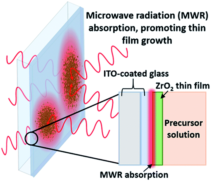 | ||
| Fig. 1 MWR-assisted synthesis. (a) MWR-assisted ZrO2 thin film synthesis on an indium tin oxide (ITO)-coated glass substrate. Localized MWR absorption by the ITO layer promotes ZrO2 nucleation and growth. | ||
For furnace-grown samples without EM field exposure, the precursor solution was spin-coated onto an ITO-coated slide, placed in the furnace at 225 °C, and held for 1 hour. Samples synthesized without EM field exposure use the spin-coating method to ensure film growth on the substrate, as no film forms on the ITO slide if it is simply held in the solution in a fashion similar to the MWR-assisted synthesis experiments.22
2.2 PDF data collection and analysis
PDF data were collected at the X-ray Powder Diffraction (XPD) beamline, 28-ID-2, at the National Synchrotron Light Source II (NSLS-II) at Brookhaven National Laboratory. Data was collected using a 2D PerkinElmer amorphous silicon detector and the rapid acquisition PDF method (RAPDF) was used.24 The sample to detector distance was 204.2 mm, and the wavelength of the monochromatic radiation was 0.1848 Å. Calibration for the measurements was done using Ni (Table S1†), and datasets were collected at room temperature.2D diffraction data were integrated using Fit2D to obtain the 1D diffraction intensities.25 Further processing was carried out using the xPDFsuite software26 to generate the PDFs, G(r), given by,
PDFgui was used for structural refinements and modeling.27 The models were fit against experimental PDFs by refining the following parameters: global and phase specific scaling factors, lattice parameters, isotropic thermal displacement parameters (Uiso), a low-r peak sharpening coefficient for correlated motion of nearby atoms (δ1),28 and a PDF peak envelope function, which dampens the signal as a function of r to account for finite structural coherence or crystallite size (Dc) in separate phases.29 Details on Dc and PDF signal dampening from finite structural coherence and instrumental broadening is given in ESI Section S1.1 and Fig. S2.† The Dc values found via PDF fitting are confirmed via TEM (Fig. S3†).
Structure files for the defect-free ZrO2 phases used in refinements were obtained from the materials project, numbers 2858 (monoclinic), 2574 (tetragonal), and 1565 (cubic). Structures used in PDF refinements were identical to those used as inputs for the defect-free DFT calculations. The goodness-of-fit, Rw, was defined as
2.3 EXAFS data collection and analysis
Zirconium K-edge spectra were collected at the Advanced Photon Source, Argonne National Laboratory, at the MR-CAT 10-ID-B beamline.30 EXAFS yields local structural information centered around a specific absorber (e.g., Zr) spanning a few coordination shells (Fig. S4†). Data was collected in fluorescence mode. Five separate spectra were collected for each sample and averaged to achieve desirable signal-to-noise ratio, and the beamline energy was calibrated using a Zr foil. A Si (111) monochromator was used to select an energy range of 17![[thin space (1/6-em)]](https://www.rsc.org/images/entities/char_2009.gif) 848 to 18850 eV.
848 to 18850 eV.
Data were processed using the Athena software and EXAFS modeling was performed in the Artemis software package.31 The amplitude reduction factor, S02, was determined to be 0.82 ± 0.04 from fitting to a Zr foil standard. During fitting, the coordination number N was then set to this value, allowing S02 to be multiplied by the expected coordination number and refined as a constraint. Thus, S02 (or N) is expected to be near a value of 1 in our refinements, with values varying from 1 indicating that the starting model may not accurately represent the coordination observed experimentally. Other constraints included the energy shift E0, change in path length ΔR, and atomic displacement parameters, σ2. E0 and ΔR were set to be equivalent for every path in all fits. σ2 values were refined independently for each path in the defect-free tetragonal, cubic, and monoclinic phases. However, for the defective ZrO1.936 structure, the number of relevant Zr–O paths was too large to independently constrain each σ2. In this case, three σ2 values were used and paths were grouped based on path length, with similar paths together. The fit range was set from 4–14 Å−1 in k-space and 1.2–3.0 Å in real-space to encompass Zr–O interatomic distances. The quality of EXAFS fits was determined by calculating an R-factor, defined as
2.4 X-ray diffraction
Laboratory X-ray diffraction (XRD) was carried out using a Panalytical X'Pert Pro MPD Diffractometer with Cu Kα radiation of wavelength 1.54 Å. A scan range of 20–85° was used, with a step size of 0.01°.2.5 In situ microwave cyclic voltammetry
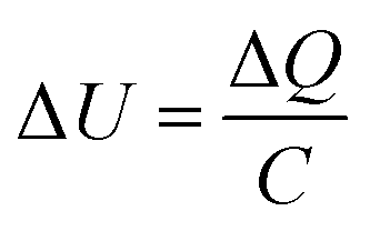
Cyclic voltammetry (CV) measurements were conducted using a Biologic SP-150 (Bio-Logic Science Instruments) at a constant scan rate of 10 mV s−1 in the voltage range of −0.5 to 0.5 V. The in situ microwave CV (MW-CV) experiments were carried out in a custom-designed microwave waveguide (Fig. S5†). Two ITO electrodes are partially submerged in a ZrO2 precursor solution, and a voltage is applied across the two electrodes as in a typical CV experiment. The corresponding change both with and without MWR is then measured (Fig. 2A and B). The underlying mechanism of the observed peaks in MW-CV and their connection to atomic structure is explored further in the Results and discussion.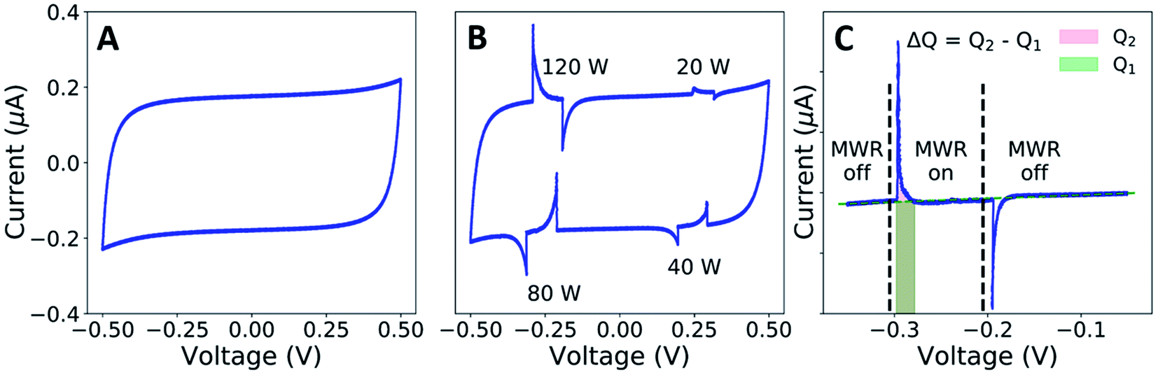 | ||
| Fig. 2 MW-CV. (A) CV results with no MWR exposure. The curve follows a loop typical of CV measurements in dielectric solutions. (B) MW-CV curve of an identical setup as in (A), but with MWR exposure. Positive peaks occur when MWR is turned on, and negative peaks occur when MWR is turned off. The peak magnitude is dependent on the MWR power applied. (C) Zoom on a single MWR on/off cycle, with the approximate times when MWR was turned on/off indicated by vertical dashed lines. The increase in surface charge due to MWR exposure, Δq, is calculated by integrating under the CV curve. The area under the curve without MWR exposure (q1, green) is subtracted from the area under the curve with MWR exposure (q2, pink) to determine Δq. | ||
The ITO-coated slides and precursor solution were held inside the waveguide while the electrode connections from the potentiostat were held outside to avoid interaction with the EM field. MWR at a frequency of 2.45 GHz was switched on/off at various voltage points and the resultant current was monitored during the scan. The solution temperature was maintained between 45–55 °C during the experiment, as determined from a fiber optic temperature sensor (Neoptix T1) inserted into the precursor solution.
The capacitance, C, of the setup was calculated from the following relationship:

where ΔU is the change in potential caused by the increase in surface charge. The corresponding electric field intensity can then be calculated by:
where E is the electric field intensity and d is the double layer thickness. d is approximated by the Debye length, found by:
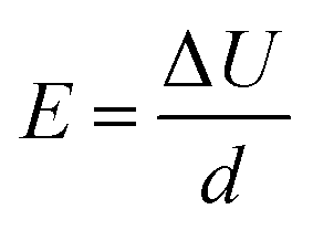
where ε is the permittivity of the solution, k is the Boltzmann constant, T is the solution temperature, e is the charge of electron, c is the concentration of Zr ions, and z is the charge of Zr. The concentration of Zr in the sol–gel precursor is 0.004 M. The permittivity of the solution is assumed to be equal to that of TEG at 50 °C, as TEG makes up the majority of the precursor solution.32 This leads to a d value of 0.6 nm. Due to the uncertainty in actual solution permittivity value, we have assumed a conservative estimate of 1 nm for double layer thickness in all calculations to ensure that the electric field intensity is not overestimated.33
2.6 Density function theory calculations
The Density Functional Theory (DFT) calculations presented used the generalized-gradient approximation and projector-augmented wave functions as implemented in VASP.34 A 566 eV planewave cutoff was used for the basis set. Ion positions and supercell lattice constants were relaxed until residual forces were less than 2 meV Å−1. A Monkhorst–Pack special k-point grid of 6 × 6 × 4 was used for the Zr2O4 primitive cell; equivalent meshes were used for the larger cells. All defect calculations were performed in charged supercells containing a single defect. We did not consider clustering of oxygen vacancies or interstitials.35 We used +2 charge states for oxygen vacancies and −2 charge states for oxygen interstitials.36,37 The excess charge was balanced via the jellium model, in which the charge compensating for the vacancies is distributed evenly across the entire simulation cell.2.7 Transmission electron microscopy
TEM samples were prepared via manual grinding, polishing, dimpling, and a final polishing step in an ion milling system (PIPS II, Gatan). Microstructure was characterized using a FEI Talos T200X transmission electron microscope operated at 200 kV.3. Results and discussion
To characterize the role of the applied field on MWR-grown ZrO2 atomic structure, we utilize synchrotron X-ray PDF analysis.38 Peaks in the PDF directly relate to interatomic distances in the atomic structure (Fig. 3A and B), allowing for quantitative characterization of short-range (SRO), medium-range (MRO), and long-range (LRO) atomic order.39 LRO and MRO correspond to higher-r regions of the PDF data and represent the crystalline atomic structure, while the SRO component represents the local atomic order. The PDF technique compliments conventional XRD. However, XRD characterizes only LRO and thus is ill-equipped to study nanoscale or locally disordered materials. The ability to characterize both local and long-range atomic structure makes PDF analysis an ideal method to investigate the influence of EM fields on structural distortions and phase stability.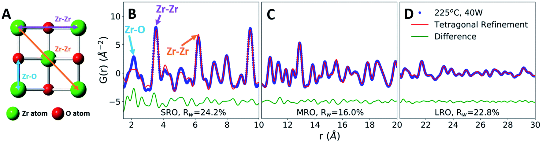 | ||
| Fig. 3 MWR-grown ZrO2. (A) Atomic structure of tetragonal ZrO2, viewed along the [001] direction. (B–D) Experimental PDF data (blue) fit to a tetragonal ZrO2 structure (red), with the difference below in green. Zr–O and Zr–Zr nearest neighbor peaks are highlighted in (B), with their corresponding interatomic distances shown in (A). Goodness-of-fit values, Rw, are shown offset below the difference curve. | ||
PDF refinements on a ZrO2 film synthesized at 225 °C and 40 W MWR power reveal tetragonal ZrO2 MRO and LRO, indicating crystalline phase formation (Fig. 3C and D). Refinements were compared with other common ZrO2 polymorphs, namely the monoclinic and cubic phases (Fig. S6†). The tetragonal phase best represents the crystalline structure observed, indicated by the lower goodness-of-fit, Rw. Despite the LRO, the SRO is not well described by the crystalline tetragonal phase, particularly with regards to nearest neighbor distances (Fig. 3B). This suggests a local Zr–O coordination environment which differs from the tetragonal phase, potentially due to symmetry lowering relaxations. Computational models have postulated that oxygen point defects can induce structural changes that impact Zr–O nearest neighbor distances and the resultant phase stability,40,41 providing one potential source of such relaxations. To investigate how defect-based local distortions impact phase stability and compare to MWR-grown ZrO2, first-principles Density Functional Theory (DFT) calculations were performed spanning a range of oxygen defect concentrations.
In defect-free ZrO2, we find that the relative energies are ordered Emonoclinic < Etetragonal < Ecubic, as expected.42 This phase stability changes as a function of oxygen defect concentration, with a defective tetragonal phase becoming energetically favorable at a vacancy concentration of 3.2% (Fig. 4A). All ZrO2 phases explored are indicated in Fig. S7 and Table S2.† The defect concentrations studied were limited by the system size of DFT calculations, yielding uncertainty regarding the exact vacancy concentration at which the defective tetragonal phase becomes favorable. However, the defective tetragonal structure shown here (ZrO1.936) contains local atomic relaxations around vacancy sites which break the local symmetry (Fig. S8 and S9†) and provides a suitable representation of oxygen vacancy-based structural distortions. This allows us to utilize the ZrO1.936 structure as a model system to explore the possibility of defect formation in MWR-grown ZrO2.
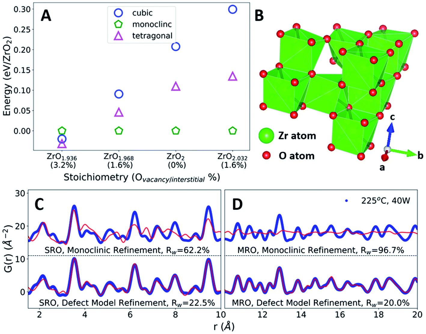 | ||
| Fig. 4 Oxygen defects, phase stability, and local atomic structure. (A) DFT-predicted energies of ZrO2 polymorphs with oxygen point defects, relative to the monoclinic phase. At high oxygen vacancy concentrations, a defective tetragonal structure becomes energetically favorable. (B) The DFT-predicted defective tetragonal structure. (C and D) PDF refinements of the monoclinic phase and DFT-predicted defect model (red) to MWR-grown ZrO2 (blue). Refinements to the SRO (C) indicate that the defective phase better represents the local atomic environment than monoclinic. Comparison with the defect-free tetragonal phase in Fig. 3B indicates that the SRO is better described by oxygen-vacancy-induced structural distortions. Refinements to the MRO confirm that the local structural distortions present from defects do not break the tetragonal structure (D). | ||
The reduced local symmetry caused by oxygen vacancies accurately represents the local atomic structure observed experimentally, as the defective model greatly improves the fit to the nearest neighbor Zr–O peak in the PDF. The lower symmetry monoclinic phase also improves the fit to nearest neighbor distances but does not describe the local order as well as the DFT-predicted defective phase (Fig. S10†). Extended X-ray absorption fine structure (EXAFS) at the Zr k-edge (1s) confirms that the defect model effectively represents the oxygen coordination environment, shown by refined values for coordination number closer to unity and a reduction in atomic displacement parameters relative to the monoclinic phase (Fig. S11 and Table S4†). PDF fitting of the defective phase to the SRO of MWR-grown ZrO2 results in a lower Rw value than the defect-free tetragonal or monoclinic phase, indicating that the local atomic order is better described by vacancy-induced relaxations (Fig. 4C). Overall, the defective phase improves the fit to the SRO while remaining consistent with the MRO and LRO observed experimentally but does not improve upon the MRO and LRO from the defect-free phase. The monoclinic phase is a poor descriptor of the observed structure beyond the nearest neighbor peaks, and conventional XRD confirms that only tetragonal LRO is present (Fig. 4D and S12†). This structural information suggests that the topology of MWR-grown ZrO2 remains tetragonal, with EM field-assisted phase stability mediated by oxygen vacancy-induced local structural distortions. The potential presence of other oxygen point defects, namely oxygen interstitials, was also investigated via PDF analysis. The DFT calculations suggest that if interstitial oxygen defects were indeed present, the monoclinic phase is expected to be stable. Due to the presence of the LRO tetragonal phase, PDF refinements to interstitial models were performed for both the monoclinic and tetragonal phases. In both cases the interstitial models resulted in poorer fits and higher Rw values than either the vacancy defect model or the defect-free phases, indicating that the addition of oxygen atoms to the lattice does not suitably describe the experimentally observed structure (Fig. S13 and S14†).
The presence of distorted local structure as a stabilizing presence in MWR-grown ZrO2 invites investigation into the mechanisms of defect formation during MWR-assisted synthesis. Experiments utilizing an identical experimental setup and heating conditions found that no phase formation occurs without MWR exposure, indicating that the chemical environment is not responsible for the observed effects.43 Synthesis using an MWR absorbing SiC vial (in place of the standard borosilicate glass) shields the growth solution from EM field exposure while maintaining similar heating rates,44 and also results in no thin film growth.22 Additionally, thin films synthesized at identical temperatures in a conventional furnace were found to have a completely disordered atomic structure (Fig. S15†). This aligns with prior work demonstrating that the ITO layer preferentially absorbs EM radiation and impacts the synthesis process.22 It is suspected that electric fields on the order of 106 V m−1, such as those present in an electric double layer, are high enough to drive ionic motion.5,6 This suggests that a potential driving force for oxygen vacancy formation is the presence of anomalously high field intensities at the substrate–solution interface. However, this local field strength has not previously been experimentally measured, making it difficult to link local electric fields with the resultant atomic structure.
To measure local electric field intensity, we developed a microwave cyclic voltammetry (MW-CV) technique capable of quantifying the change in electric field at the ITO layer due to MWR exposure. MW-CV represents the first experimental technique capable of monitoring local electric field intensities for EM field-assisted synthesis. When MWR is applied to the system, a positive spike in the current is observed. Conversely, when MWR is removed, a negative spike in the current occurs (Fig. 5A). This change in current is related to a buildup of surface charge, from which the electric field intensity can be calculated. More details on the MW-CV measurements and resultant electric field intensity calculations can be found in Materials and methods Section 2.5. At 40 W of applied power, the increase in measured current due to MWR corresponds to an electric field on the order of 106 V m−1, orders of magnitude higher than prior predictions in EM field-assisted processes.45 The dependence of field intensity on interactions between MWR and the substrate material is demonstrated by an order of magnitude increase in local electric field intensity, up to 107 V m−1, when replacing one ITO layer with a higher electrical conductivity Ti layer (Fig. 5B and S16†). Additionally, varying the H+ concentration in the solution to alter the interaction between MWR and the solution led to an increase in the peak intensity and faster ionic motion to the ITO surface, but no significant change in the electric field intensity (Fig. 5C, S17 and S18†). These results indicate that MWR absorption by the conducting layer is essential to the high electric field intensities observed. Prior work related to EM field absorption in materials has demonstrated that MWR absorption results in an electric field strength distribution at the material surface.46–48 This electric field buildup at the ITO layer draws ions to the surface, resulting in the formation of an electric double layer and a positive spike in the measured current to balance the additional surface charge. The high electric field present in the electric double layer is what is measured experimentally during MW-CV measurements, as opposed to the smaller electric field formed from MWR absorption by the ITO which promotes double layer formation. When MWR is removed from the system, the ions drawn to the surface release back to a random orientation, resulting in the negative spike in current observed. This process is shown schematically in Fig. 5D–F.
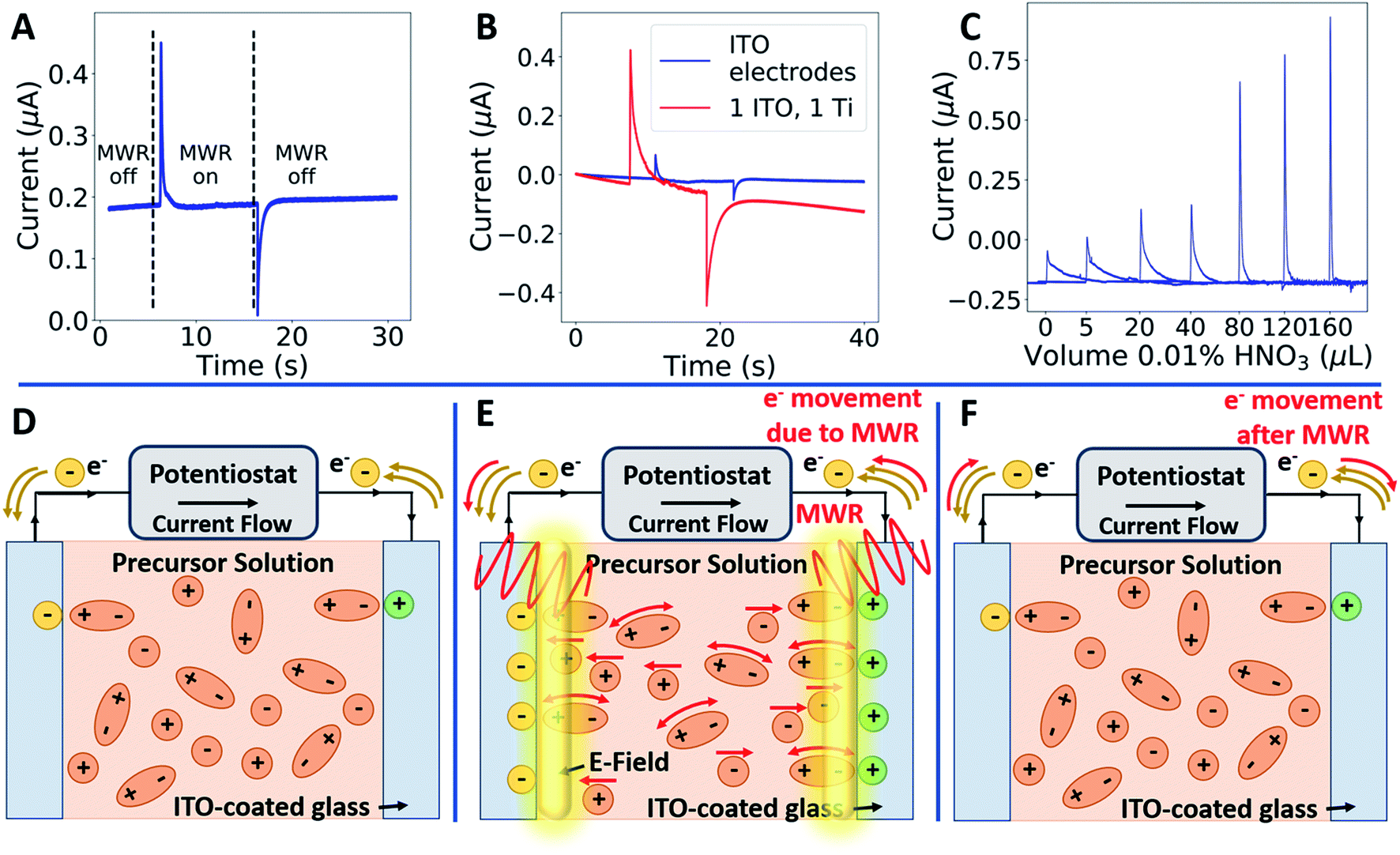 | ||
| Fig. 5 Local electric field intensity due to MWR exposure. (A) MW-CV measurements indicating the change in current when the MWR is turned on (positive spike) and off (negative spike). (B) The role of the substrate during MW-CV measurements. (C) The role of ion concentration on measured current. (D–F) The mechanism of local electric field enhancement during MWR exposure. Initially, polar molecules and ions are oriented randomly in solution (D). MWR is absorbed by the conducting layer, creating an electric field at the surface. This draws additional ions or molecules to the surface, leading to a spike in current to balance the additional surface charge and a large local electric field due to the formation of an electric double layer (E). When MWR is turned off, the ions drawn to the surface release back to a random orientation, leading to a sharp negative flow in current (F). | ||
The magnitude of the electric field intensity is found to increase with increasing MWR power levels, with higher power levels leading to higher electric field intensities (Fig. 6A). Despite the increase in field intensity, the LRO of all films remains consistent with the tetragonal phase (Fig. 6B). The SRO, however, experiences changes based on applied power. Higher electric field intensities promote more local atomic distortions, suggesting that higher power levels can induce more defects on the oxygen sub-lattice. This effect can be deduced from a noticeable change in the nearest neighbor peaks in the PDF data, leading to a decreasing quality of fit to the defective model structure (Fig. 6C). EXAFS spectra confirm this trend, with broader and less intense Zr–O peaks indicative of more structural disorder present at higher electric field intensities (Fig. 6D). This increased structural disorder is not correlated to the grain size, as the average size found from PDF modeling remains similar regardless of the MWR power level (Table S3†). This observation suggests that higher local electric field magnitudes can impact defect concentrations and local structural changes without breaking the crystalline LRO of a material.
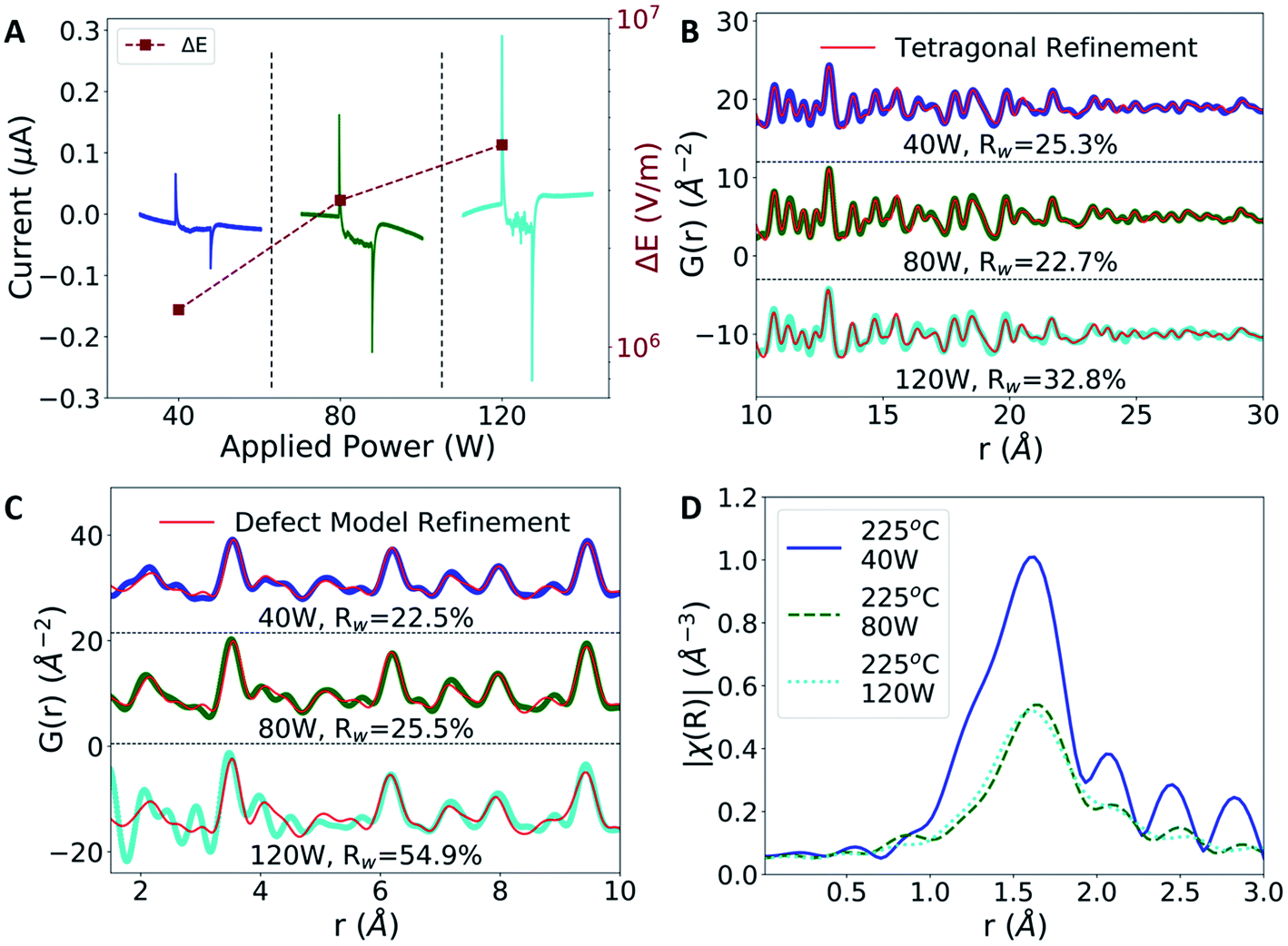 | ||
| Fig. 6 Effects of MWR power on local electric field intensity and atomic structure. (A) Higher applied power leads to higher local electric fields at the ito layer. (B) Higher power levels do not eliminate the LRO tetragonal phase, as shown by tetragonal refinements (red) to MWR-grown ZrO2 synthesized at 225 °C and 40, 80, and 120 W. (C) The SRO is impacted by the power level, as shown by refinements to the defective model (red). (D) EXAFS spectra indicating additional local atomic disorder with increasing MWR power, as seen by the broadening and decrease in intensity of Zr–O peaks at higher power levels. This suggests that larger local electric fields can promote higher defect concentrations and can increase local atomic disorder without sacrificing the overall tetragonal topology. | ||
While no prior studies have experimentally linked local electric field strengths with local atomic structure, evidence exists to support the claim that applied fields can influence defect formation. In electric field-assisted sintering of yttria-stabilized zirconia, it has been suggested that the injection of additional carriers can lower defect formation energy.49 Additionally, polarization effects have been found to lower oxygen vacancy formation energy in oxide materials.50 Previous work has also found that suspected high electric fields at interfaces can drive ionic motion, influencing defect concentrations and phase transitions.5,6 This evidence, coupled with the local electrical and structural characterization presented here, suggests that high local electric field strengths can serve as a driving force for defect-based structural changes during ceramic synthesis.
4. Conclusion
We use a unique blend of materials chemistry, electromagnetics, and engineering methods to demonstrate that high local electric fields can serve as a driving force for local structural changes which impact phase stability during EM field-assisted ceramic growth. High electric fields are present even while a ceramic oxide layer is present on the substrate (Fig. S19†) and prior experiments have demonstrated the success of MWR-assisted synthesis on particles that are not electrically conducting.43 This indicates that local EM field absorption, regardless of the electrical properties of the absorber, can promote material growth. With this evidence, we have obtained new insight into how synthesis and phase transitions progress under EM excitation, demonstrating that local electric field strengths are dependent on the applied power and can impact local atomic order without significantly altering the crystalline atomic structure. With these new insights, complementary directions open up for further exploring the role of EM field effects during ceramic synthesis. For example, high resolution scanning transmission electron microscopy (STEM) can potentially image local defect structure near the ITO-thin film interface. Finally, the characterization approaches such as the MW-CV technique introduced here provides a template for future studies to investigate the interplay between EM fields, local structure, and phase stability in a variety of material systems. Our work thus lays the practical and theoretical foundations for deploying EM fields as a synthesis tool to access new materials with minimal thermal input, enabling exploration of regions of phase space, microstructures, and properties not accessible via conventional chemical synthesis routes. Understanding such field-driven structural transitions also has important implications in engineering low temperature techniques to integrate ceramics with temperature-sensitive polymer materials for flexible electronics and in tailoring ceramic properties for energy generation and storage applications.Author contributions
B. R. J. and N. N. designed the experiments. N. N. performed the majority of the PDF and EXAFS data analysis with input from all authors. E. C. and S. J. L. B. performed the PDF data collection. L. S. and S. K. J. performed the EXAFS data collection. N. N. and L. S. developed the MW-CV experimental setup, performed MW-CV experiments, and analyzed MW-CV data. H. W. and H. W. collected the TEM images. C. S. H. and N. B. performed DFT calculations and analysis. The manuscript was written by N. N. and B. R. J. with input from all authors.Conflicts of interest
There are no conflicts of interest to declare.Acknowledgements
Funding: B. R. J. and N. N. acknowledge the U.S. Department of Defense (DoD), Air Force Office of Scientific Research (AFOSR) award number FA9550-17-1-0120, directed by Dr Ali Sayir. N. N. is supported by the DoD through the National Defense Science & Engineering Graduate Fellowship (NDSEG) Program. PDF data collection by S. J. L. B. and E. C. was supported by US DOE, Office of Science, Office of Basic Energy Sciences under contract DE-SC0012704. C. S. H. and N. B. were supported by the Office of Naval Research and in part by a grant of computer time from the DoD High Performance Computing Modernization Program at the AFRL Supercomputing Resource Center. H. W. and H. W. acknowledge support for TEM measurements from the Office of Naval Research (contract no. N00014-16-1-2778). For PDF measurements, this research used beamline 28-ID-2 of the National Synchrotron Light Source II, a U.S. Department of Energy (DOE) Office of Science User Facility operated for the DOE Office of Science by Brookhaven National Laboratory under Contract No. DE-SC0012704. For EXAFS measurements, MRCAT operations are supported by the Department of Energy and the MRCAT member institutions. This research used resources of the Advanced Photon Source, a U.S. Department of Energy (DOE) Office of Science User Facility operated for the DOE Office of Science by Argonne National Laboratory under Contract No. DE-AC02-06CH11357. The authors acknowledge use of the Materials Characterization Facility at Carnegie Mellon University supported by grant MCF-677785.References
- J. M. Lebrun, G. Morrissey Timothy, S. C. Francis John, C. Seymour Kevin, M. Kriven Waltraud and R. Raj, J. Am. Ceram. Soc., 2015, 98, 1493–1497 CrossRef CAS.
- N. Nakamura, M. Terban, S. J. L. Billinge and B. Reeja-Jayan, J. Mater. Chem. A, 2017, 5, 18434–18441 RSC.
- M. Baghbanzadeh, L. Carbone, P. D. Cozzoli and C. O. Kappe, Angew. Chem., Int. Ed., 2011, 50, 11312–11359 CrossRef CAS PubMed.
- M. Yu, S. Grasso, R. McKinnon, T. Saunders and M. J. Reece, Adv. Appl. Ceram., 2017, 116, 24–60 CrossRef CAS.
- J. Jeong, N. Aetukuri, T. Graf, T. D. Schladt, M. G. Samant and S. S. P. Parkin, Science, 2013, 339, 1402 CrossRef CAS PubMed.
- N. Lu, P. Zhang, Q. Zhang, R. Qiao, Q. He, H.-B. Li, Y. Wang, J. Guo, D. Zhang, Z. Duan, Z. Li, M. Wang, S. Yang, M. Yan, E. Arenholz, S. Zhou, W. Yang, L. Gu, C.-W. Nan, J. Wu, Y. Tokura and P. Yu, Nature, 2017, 546, 124 CrossRef CAS PubMed.
- S. Chen, Z. Wang, H. Ren, Y. Chen, W. Yan, C. Wang, B. Li, J. Jiang and C. Zou, Sci. Adv., 2019, 5, eaav6815 CrossRef CAS PubMed.
- S. K. Jha, X. L. Phuah, J. Luo, C. P. Grigoropoulos, H. Wang, E. García and B. Reeja-Jayan, J. Am. Ceram. Soc., 2019, 102, 5–31 CrossRef CAS.
- R. Raj, M. Cologna and J. S. C. Francis, J. Am. Ceram. Soc., 2011, 94, 1941–1965 CrossRef CAS.
- K. I. Rybakov, E. A. Olevsky and E. V. Krikun, J. Am. Ceram. Soc., 2013, 96, 1003–1020 CrossRef CAS.
- M. Cologna, B. Rashkova and R. Raj, J. Am. Ceram. Soc., 2010, 93, 3556–3559 CrossRef CAS.
- J. Narayan, Scr. Mater., 2013, 69, 107–111 CrossRef CAS.
- W. Ji, B. Parker, S. Falco, J. Y. Zhang, Z. Y. Fu and R. I. Todd, J. Eur. Ceram. Soc., 2017, 37, 2547–2551 CrossRef CAS.
- S. Komarneni, Q. Li, K. M. Stefansson and R. Roy, J. Mater. Res., 1993, 8, 3176–3183 CrossRef CAS.
- Q. Liu, M. R. Gao, Y. Liu, J. S. Okasinski, Y. Ren and Y. Sun, Nano Lett., 2016, 16, 715–720 CrossRef CAS PubMed.
- N. Nakamura, L. Su, J. Bai, S. Ghose and B. Reeja-Jayan, J. Mater. Chem. A, 2020, 8, 15909–15918 RSC.
- J. M. Lebrun, C. S. Hellberg, S. K. Jha, W. M. Kriven, A. Steveson, K. C. Seymour, N. Bernstein, S. C. Erwin and R. Raj, J. Am. Ceram. Soc., 2017, 100, 4965–4970 CrossRef CAS.
- S. K. Jha, H. Charalambous, H. Wang, X. L. Phuah, C. Mead, J. Okasinski, H. Wang and T. Tsakalakos, Ceram. Int., 2018, 44, 15362–15369 CrossRef CAS.
- B. Yoon, D. Yadav, R. Raj, E. P. Sortino, S. Ghose, P. Sarin and D. Shoemaker, J. Am. Ceram. Soc., 2018, 101, 1811–1817 CrossRef CAS.
- R. J. Kamaladasa, A. A. Sharma, Y. T. Lai, W. Chen, P. A. Salvador, J. A. Bain, M. Skowronski and Y. N. Picard, Microsc. Microanal., 2015, 21, 140–153 CrossRef CAS PubMed.
- J. Li, J. Cho, J. Ding, H. Charalambous, S. Xue, H. Wang, X. L. Phuah, J. Jian, X. Wang, C. Ophus, T. Tsakalakos, R. E. García, A. K. Mukherjee, N. Bernstein, C. S. Hellberg, H. Wang and X. Zhang, Sci. Adv., 2019, 5, eaaw5519 CrossRef CAS PubMed.
- B. Reeja-Jayan, K. L. Harrison, K. Yang, C.-L. Wang, A. E. Yilmaz and A. Manthiram, Sci. Rep., 2012, 2, 1003 CrossRef CAS PubMed.
- N. Nakamura, J. Seepaul, J. B. Kadane and B. Reeja-Jayan, Appl. Stoch. Model. Bus. Ind., 2017, 33, 314–321 CrossRef.
- P. J. Chupas, X. Qiu, J. C. Hanson, P. L. Lee, C. P. Grey and S. J. L. Billinge, J. Appl. Cryst., 2003, 36, 1342–1347 CrossRef CAS.
- A. P. Hammersley, S. O. Svensson, M. Hanfland, A. N. Fitch and D. Hausermann, High Pressure Res, 1996, 14, 235–248 CrossRef.
- X. Yang, P. Juhas, C. L. Farrow and S. J. L. Billinge, 2014, arXiv, 1402.3163.
- C. L. Farrow, P. Juhas, J. W. Liu, D. Bryndin, E. S. Božin, J. Bloch, T. Proffen and S. J. L. Billinge, J. Phys. Condens. Matter, 2007, 19, 335219 CrossRef CAS PubMed.
- I. K. Jeong, T. Proffen, F. Mohiuddin-Jacobs and S. J. L. Billinge, J. Phys. Chem. A, 1999, 103, 921–924 CrossRef CAS.
- K. Kodama, S. Iikubo, T. Taguchi and S. Shamoto, Acta Crystallogr., Sect. A: Found. Crystallogr., 2006, 62, 444–453 CrossRef PubMed.
- C. U. Segre, N. E. Leyarovska, L. D. Chapman, W. M. Lavender, P. W. Plag, A. S. King, A. J. Kropf, B. A. Bunker, K. M. Kemner, P. Dutta, R. S. Duran and J. Kaduk, AIP Conf. Proc., 2000, 521, 419–422 CrossRef.
- B. Ravel and M. Newville, J. Synchrotron Rad., 2005, 12, 537–541 CrossRef CAS PubMed.
- N. Koizuim and T. Hanai, J. Phys. Chem., 1956, 60, 1496–1500 CrossRef.
- R. Kötz and M. Carlen, Electrochim. Acta, 2000, 45, 2483–2498 CrossRef.
- G. Kresse and D. Joubert, Phys. Rev. B: Condens. Matter Mater. Phys., 1999, 59, 1758–1775 CrossRef CAS.
- C. Freysoldt, B. Grabowski, T. Hickel, J. Neugebauer, G. Kresse, A. Janotti and C. G. Van de Walle, Rev. Mod. Phys., 2014, 86, 253–305 CrossRef.
- J. X. Zheng, G. Ceder, T. Maxisch, W. K. Chim and W. K. Choi, Phys. Rev. B: Condens. Matter Mater. Phys., 2007, 75, 104112 CrossRef.
- B. Liu, H. Xiao, Y. Zhang, D. S. Aidhy and W. J. Weber, Comput. Mater. Sci., 2014, 92, 22–27 CrossRef CAS.
- K. M. Ø. Jensen, A. B. Blichfeld, S. R. Bauers, S. R. Wood, E. Dooryhée, D. C. Johnson, B. B. Iversen and S. J. L. Billinge, IUCrJ, 2015, 2, 481–489 CrossRef CAS PubMed.
- T. Egami and S. J. L. Billinge, Underneath the Bragg Peaks: Structural Analysis of Complex Materials, Elsevier, 2012 Search PubMed.
- S. Fabris, A. T. Paxton and M. W. Finnis, Acta Mater., 2002, 50, 5171–5178 CrossRef CAS.
- F. Zhang, P. J. Chupas, S. L. A. Lui, J. C. Hanson, W. A. Caliebe, P. L. Lee and S.-W. Chan, Chem. Mater., 2007, 19, 3118–3126 CrossRef CAS.
- P. Bouvier, E. Djurado, G. Lucazeau and T. Le Bihan, Phys. Rev. B: Condens. Matter Mater. Phys., 2000, 62, 8731–8737 CrossRef CAS.
- S. K. Jha, N. Nakamura, S. Zhang, L. Su, P. M. Smith, X. L. Phuah, H. Wang, H. Wang, J. S. Okasinski, A. J. H. McGaughey and B. Reeja-Jayan, Adv. Eng. Mater., 2019, 21, 1900762 CrossRef CAS.
- B. Gutmann, D. Obermayer, B. Reichart, B. Prekodravac, M. Irfan, J. M. Kremsner and C. O. Kappe, Chem. –Eur. J., 2010, 16, 12182–12194 CrossRef CAS PubMed.
- T. B. Holland, U. Anselmi-Tamburini, D. V. Quach, T. B. Tran and A. K. Mukherjee, J. Eur. Ceram. Soc., 2012, 32, 3659–3666 CrossRef CAS.
- K. Li, J. Xu, X. Yan, L. Liu, X. Chen, Y. Luo, J. He and D. Z. Shen, Appl. Phys. Lett., 2016, 108, 183102 CrossRef.
- J. Meixner, IEEE Trans. Antennas Propag., 1972, 20, 442–446 CrossRef.
- T. Galek, K. Porath, E. Burkel and U. van Rienen, Modelling Simul. Mater. Sci. Eng., 2010, 18, 025015 CrossRef.
- H. Wang, X. L. Phuah, J. Li, T. B. Holland, K. S. N. Vikrant, Q. Li, C. S. Hellberg, N. Bernstein, R. E. García, A. Mukherjee, X. Zhang and H. Wang, Ceram. Int., 2019, 45, 1251–1257 CrossRef CAS.
- M. Youssef, K. J. Van Vliet and B. Yildiz, Phys. Rev. Lett., 2017, 119, 126002 CrossRef PubMed.
Footnote |
| † Electronic supplementary information (ESI) available. See DOI: 10.1039/d1ta00486g |
| This journal is © The Royal Society of Chemistry 2021 |