
Performance improvement of MXene-based perovskite solar cells upon property transition from metallic to semiconductive by oxidation of Ti3C2Tx in air†
Lin
Yang
a,
Dongxiao
Kan
a,
Chunxiang
Dall'Agnese
 a,
Yohan
Dall'Agnese
b,
Baoning
Wang
a,
Ajay Kumar
Jena
c,
Yingjin
Wei
a,
Gang
Chen
a,
Xiao-Feng
Wang
*a,
Yury
Gogotsi
d and
Tsutomu
Miyasaka
c
a,
Yohan
Dall'Agnese
b,
Baoning
Wang
a,
Ajay Kumar
Jena
c,
Yingjin
Wei
a,
Gang
Chen
a,
Xiao-Feng
Wang
*a,
Yury
Gogotsi
d and
Tsutomu
Miyasaka
c
aKey Laboratory of Physics and Technology for Advanced Batteries (Ministry of Education), College of Physics, Jilin University, 2699 Qianjin Street, Changchun 130012, China. E-mail: xf_wang@jlu.edu.cn
bInstitute for Materials Discovery, University College London, London WC1E 7JE, UK
cGraduate School of Engineering, Toin University of Yokohama, 1614 Kurogane-cho, Aoba, Yokohama, Kanagawa 225-8503, Japan
dDepartment of Materials Science and Engineering, and A. J. Drexel Nanomaterials Institute, Drexel University, Philadelphia, Pennsylvania 19104, USA
First published on 28th January 2021
Abstract
The unique properties of MXenes that arise from terminating functional groups and oxidation of MXenes make them attractive for application in photovoltaic devices like perovskite solar cells (PSCs). Here, oxidation of Ti3C2Tx hydrocolloid was carried out to tune its properties desirable for an electron transport layer (ETL) in low-temperature processed PSCs. The calculations of the energy levels were carried out using the Vienna ab initio simulation package (VASP) code based on density functional theory (DFT). Oxidation of Ti3C2Tx can generate Ti–O bonds and effectively reduce the macroscopic defects of the film fabricated by spin-coating, while a transition from metallic material to semiconductor occurred after heavy oxidation. A better matching of energy levels between perovskite and ETL layer in the case of a hybrid of oxidized and pristine Ti3C2Tx renders a champion power conversion efficiency (PCE) of 18.29%. The improvement in PCE can be attributed to the increased electron mobility in the ETL, which promotes electron transport and reduces the electron–hole recombination. Hence, by presenting a simple method for high performance in PSCs by MXene-derived materials, this work demonstrates the great potential of these materials for applications in low-temperature processed PSCs and other photovoltaic technologies.
Introduction
The rapid development of organic–inorganic lead halide perovskite solar cells (PSCs) has gained enormous attention. They are promising candidates owing to their high mobility, appropriate bandgap, long carrier diffusion length and strong absorption coefficients in the visible spectrum.1–4 The power conversion efficiency (PCE) has risen from 3.8% to 25.5%,5,6 demonstrating the immense potential of this competitive photovoltaic technology. In the PSCs, the electron transport layer (ETL) is an essential component in restraining charge recombination and rectifying the photocurrent.7 The traditional mesoporous structured PSCs based on TiO2 as ETL usually deliver high efficiency and stable power output, but the need of sintering limits their utilization. Low-temperature processed PSCs are more promising due to their simple fabrication and low cost.8–10 Recently, two-dimensional (2D) materials have attracted attention for application in low-temperature processed PSCs.11,12 For example, Jokar et al. reported rGO-based inverted PSC with a PCE of 16%.13 Fu et al. explored ultrasmall black phosphorus quantum dots as ETL in PSCs, and a maximum PCE of 11.26% was achieved for the devices based on flexible substrates.14 Singh et al. explored MoS2 as ETL and achieved a PCE of 13.14%, and Yin et al. obtained a PCE of 17.37% using 2D TiS2 as ETL for planar PSCs.15,16MXenes are 2D transition metal carbides and nitrides with a formula of Mn+1XnTx, where M represents an early transition metal, X indicates carbon and/or nitrogen, and Tx represents the surface terminations (usually –O, –OH and/or –F).17,18 Owing to their excellent electrical conductivity, flexibility, hydrophilicity and rich and tunable surface chemistry,19,20 MXenes have been explored in supercapacitors,21 lithium-ion batteries,22 sensors,23 electromagnetic interference shielding24 and catalysis.25 In addition, the oxidation and environmental stability have been extensively studied. New applications in energy and catalysis emerged for partially oxidized MXenes.26 Moreover, applications of Ti3C2Tx in solar cells have also been explored. Ti3C2Tx, which has metallic conductivity, has been applied as electrode in dye-sensitized solar cells and as an additive to perovskite layer or ETLs for perovskite solar cells.27–29 Ti3C2Tx has also been employed as an interfacial layer to optimize the interface band alignment between perovskite and ETL, resulting in a PCE exceeding 20%.30 Yu et al. tested Ti3C2Tx as electron- and hole-transport layers in organic solar cells and a PCE of 9.06% was achieved.31 Besides, a multi-dimensional conductive heterojunction structure, composited of TiO2, SnO2, and Ti3C2Tx MXene was designed and applied as ETL by Huang et al., achieving 19.14% PCE.32 The work function tuning of Ti3C2Tx by controlling the surface termination group was demonstrated by Schultz et al.33 and used by Di Vito et al. to achieve better matching of energy levels and effective charge transport.34 Our previous work showed that UV-ozone treatment of Ti3C2Tx can effectively generate oxide-like Ti–O bonds, rendering it suitable as ETL in PSCs and a PCE of 17.17% was demonstrated.35 The removal of OH terminations and formation of Ti–O bonds can effectively improve the interface properties of the Ti3C2Tx/perovskite junction and result in better PCE, which aroused our interest in exploring Ti3C2Tx oxidized to varying degrees as ETLs for PSCs.
In this work, Ti3C2Tx colloidal solution in water was placed onto a hot plate at 50 °C under continuous magnetic stirring in ambient air to control its oxidation process. Varying degrees of oxidation of Ti3C2Tx were prepared, including lightly oxidized Ti3C2Tx (LO-Ti3C2Tx) and heavily oxidized Ti3C2Tx (HO-Ti3C2Tx), as well as a composite of heavily oxidized Ti3C2Tx with pristine Ti3C2Tx (HO-Ti3C2Tx@Ti3C2Tx). These nanomaterials were spin-coated on indium tin oxide (ITO) substrates to serve as ETLs for the low-temperature processed PSCs with the structure of ITO/ETL/CH3NH3PbI3/spiro-OMeTAD/Ag. Scanning electron microscopy (SEM), transmission electron microscopy (TEM) and X-ray photoelectron spectroscopy (XPS) indicate that appropriate oxidation of Ti3C2Tx can reduce the macroscopic defects of the film, generate more Ti–O bonds and render the material more suitable as ETLs in PSCs. Moreover, the computational analysis of oxidized Ti3C2Tx was conducted using the Vienna ab initio simulation package (VASP) code based on density functional theory (DFT). A transition from metallic material to semiconductor for Ti3C2Tx occurred by oxidation, while a better matching of energy levels was obtained. The device based on HO-Ti3C2Tx@Ti3C2Tx showed an increase in short-circuit current density (Jsc) and fill factor (FF), resulting in PCE of 18.29%. A better surface homogeneity of the film and decreased electron–hole recombination at the ETL/perovskite interface enhanced the electron mobility and further promoted electron transport, resulting in improvement of PCE.
Experimental section
Materials
Methylammonium iodide (CH3NH3I, >99.5%), lead iodide (PbI2, >99.99%) and lithium-bis(trifluoromethanesulfonyl)imide (Li-TFSI, >99%) were purchased from Xian Polymer Light Technology Corp. 2,2′,7,7′-Tetrakis-(N,N-di-p-methoxyphenylamino)-9,9′-spirobifluorene (spiro-OMeTAD, >99.8%), 4-tert-butyl pyridine (tBP, 96%) and ultra-dry anhydrous N,N-dimethylformamide (DMF, 99.8%) and dimethyl sulfoxide (DMSO, 99.7%) were purchased from Sigma Aldrich. For MAX phase synthesis, titanium powder and aluminum powder were purchased from Aladdin. Graphite was purchased from Sigma Aldrich.Preparation of Ti3C2Tx MXene colloidal solution
The method is the same as our previous report.35 The mixture of titanium powder (7.368 g), aluminum powder (1.523 g) and graphite (1.109 g) was sintered at 1650 °C for 2 hours under argon to prepare Ti3AlC2 MAX phase. Then we used a mortar-pestle to grind the Ti3AlC2 MAX powder and make it pass through the 400 mesh sieve. The obtained uniform Ti3AlC2 MAX powder was added into 12 M LiF/9 M HCl solution at room temperature. Specifically, 1.6 g LiF was added while continuously stirring 20 mL of 9 M HCl solution at room temperature and stirred for a few minutes. Then 1.0 g Ti3AlC2 MAX powder was gradually added (about 5 min) to the etchant solution and continuously etched for 24 h at room temperature. When the etching process was finished, the obtained acid mixture was repeatedly washed with deionized water by centrifugation (5 min per cycle at 8000 rpm) until the pH of mixture was over 5. Finally, the slurry was placed in ultrasound for 30 min in an ice bath under argon and centrifuged at 3500 rpm for 1 h. The obtained supernatant was the colloid solution of Ti3C2Tx nanosheets. To confirm and control the concentration, a known quantity of solution was filtered over a cellulose membrane (0.22 μm pore size). After weighing the peeled-off dried Ti3C2Tx film, the concentration of Ti3C2Tx was determined, and also could be tuned.Oxidation of MXene and preparation of solutions for ETL
By diluting the as-prepared highly concentrated Ti3C2Tx dispersion with deionized water, the Ti3C2Tx colloidal solution with an appropriate concentration of 3 mg mL−1 was obtained. Then the colloidal solution was placed on a hot plate at 50 °C under continuously stirring for 48 h to obtain LO-Ti3C2Tx and 120 h to obtain HO-Ti3C2Tx. The HO-Ti3C2Tx@Ti3C2Tx were obtained by mixing the two solutions together directly in a certain proportion and stirring for 5 min before using. Unless specified otherwise, the HO-Ti3C2Tx@Ti3C2Tx data presented in this article were obtained with the composite with a 5![[thin space (1/6-em)]](https://www.rsc.org/images/entities/char_2009.gif) :1 ratio (HO-Ti3C2Tx:Ti3C2Tx).
:1 ratio (HO-Ti3C2Tx:Ti3C2Tx).
Device fabrication
The detailed method for the device fabrication referred to our previous work.35 The pre-patterned ITO-coated substrates were washed by ultrasonication with deionized water, acetone, alcohol, and isopropanol for 30 min respectively, then dried and treated with UV ozone for 30 min. To fabricate ETLs, Ti3C2Tx colloid and the composites of oxidized Ti3C2Tx and Ti3C2Tx were prepared via spin-coating 80 μL of the colloid onto the ITO substrates at 2500 rpm for 60 s in air, followed by thermal annealing on a hot plate at 100 °C for 30 min and UV ozone treatment for 30 min. Then the samples were moved into a glovebox filled with argon to fabricate the perovskite (CH3NH3PbI3) layer, whose precursor solution was prepared by mixing 1.3 M (242 mg) PbI2 and 1.3 M (83 mg) CH3NH3I in 408 μL DMF/DMSO (4:1 volume ratio) and stirring for more than 60 min. The perovskite layer was prepared by depositing its precursor solution (45 μL) via spin-coating at 5000 rpm for 30 s onto the ETL, and 350 μL chlorobenzene was injected quickly onto the film in 5 s during the spin-coating process. The obtained film was then annealed at 100 °C for 10 min on a hot plate. After that, the spiro-OMeTAD was dissolved in chlorobenzene (80 mg mL−1) under continuous stirring for 20 min. Then, 10.5 μL of tBP and 15.5 μL of a Li-TFSI solution (510 mg Li-TFSI/1 mL acetonitrile) were added into 1 mL solution and spin-coated onto the perovskite layer at a speed of 4000 rpm for 30 s. Then the samples were kept in the dark at room temperature overnight in dry air. Finally, 60 nm Ag electrode was deposited on the top of spiro-OMeTAD by thermal evaporation.
Simulation characterization
The calculations were carried out by the Vienna ab initio simulation package (VASP) code based on density functional theory (DFT). The exchange–correlation function based on generalized gradient approximation (GGA) with the Perdue–Burke–Ernzerhof (PBE) was employed. The ion–electron interaction was treated by the projector augmented wave (PAW) method. The energy cutoff was set at 500 eV, the Brillouin-zone integrations and the magnitude of the force acting on each atom became less than 0.01 eV Å−1. The Brillouin zone was represented by Monkhorst–Pack special k-point mesh of 5 × 5 × 1 for geometry optimizations of Ti3C2Tx (X = O; F; OH), 20%-oxidized Ti3C2Tx, 80%-oxidized Ti3C2Tx, HO-Ti3C2Tx@Ti3C2Tx composite, and 9 × 9 × 9 for TiO2 bulk, respectively. The positions of atoms and the cell parameters were fully optimized by using the conjugate gradient method and the total energy of the optimized structures were well converged to 10−6 eV per cell. The electronic structures including density of states (DOS) and band gap were obtained using k point of 11 × 11 × 1 Monkhorst–Pack k-point grid. A large vacuum space of 15 Å was used for avoiding any interaction between MXene layers. Besides, the van der Waals interaction was considered, and DFT+U correction was used during our calculations with the U value of 3 V for Ti atoms.The relaxed lattice parameters for TiO2 bulk was a = b = 4.67 Å, c = 3.03 Å while a = b = 3.10 Å for Ti3C2Tx, respectively, which were all in consistent with previous experimental and theoretical values.36 The structure of TiO2–Ti3C2Tx heterojunction was constructed by a 2 × 2 (010) surface of TiO2 and a 1 × 1 (001) surface of Ti3C2Tx. Besides, 20%-oxidized Ti3C2Tx for LO-Ti3C2Tx, 80%-oxidized Ti3C2Tx for HO-Ti3C2Tx were constructed with the model of surface inside heterojunction.37,38
Thin film characterization
The UV-ozone treatment was employed by BZS250GF-TS UV-ozone cleaner. The UV/vis absorption spectra of ETLs films were characterized by a Shimadzu UV-1900 spectrophotometer over the 300–1000 nm wavelength range. ETLs were coated on glass then their crystal structures were characterized by X-ray diffraction (XRD) (Brucker D8 X-ray diffractometer) with Cu Kα radiation (λ = 1.5418 Å) at room temperature. The data was collected with a 0.02° step size (2θ) for 0.2 s. Raman spectra were obtained by Raman spectroscopy (Spex 1403) with a 514 nm laser to identify the molecular structure. XPS measurements were performed using Thermo Fischer ESCALAB 250Xi. SEM images were acquired by a field emission scanning electron microscope (Hitachi SU8000). TEM images were recorded using a JEM-2200FS (JEOL). Steady-state photoluminescence (PL) was carried out by Shimadzu RF-5301PC spectrophotometer with excitation at 403 nm on the perovskite surface. Time-resolved photoluminescence (TRPL) spectra were carried out by a PL spectrometer (Edinburgh Instruments, FLS 920). Ultraviolet photoelectron spectra (UPS) were determined by PHI5000 VersaProbe III (scanning ESCA microprobe) SCA (Spherical Analyzer).Device characterization
The J–V characteristics of perovskite solar cells were measured by a Keithley 2400 source meter measurement system with an AM 1.5 G filter at an illumination intensity of 100 mW cm−2. The effective area of the cells was confirmed to be 0.04 cm2 using a non-reflective metal mask. The EQE spectra were measured in air under short-circuit conditions using SOFN 7-SCSpecIII equipped with a 100 W Xe arc lamp, a filter wheel, and a monochromator. Monochromatic light was chopped at a frequency of 80 Hz and photocurrents were measured using a lock-in amplifier. The setup was calibrated using a certified silicon reference diode of known spectral response. The electrochemical impedance spectroscopy (EIS) measurements on the devices were carried out by a VSP multi-channel potentiostat (Biologic, France), under the standard AM 1.5 G (100 mW cm−2) simulated sunlight illumination at open-circuit potential with the frequency ranging between 1 MHz and 10 Hz. Z-View Analyst software was used to model the Nyquist plots obtained from the impedance measurements.Results and discussion
In situ oxidation of Ti3C2Tx nanosheets and characterization of the films
The Ti3C2Tx MXene nanosheets were fabricated following our previous work by etching the Al layers from Ti3AlC2 MAX phase and exfoliating the MXene via the minimally intensive layer delamination (MILD) method.39 Then, the Ti3C2Tx colloidal solution was placed on a hot plate at 50 °C under continuous stirring to oxidize it. The photos of different samples after oxidation are shown in Fig. 1a–d. As the stirring time increases to 48 h, partial oxidation occurred and the initial dark black color of the Ti3C2Tx colloid solution became lighter (see Fig. 1b), named as LO-Ti3C2Tx. After 120 h of stirring, the Ti3C2Tx has been mostly oxidized and the dark colloid solution turned to grey, which is shown in Fig. 1c and named as HO-Ti3C2Tx. Mixtures of HO-Ti3C2Tx and pristine Ti3C2Tx solutions were prepared in different proportions directly to obtain the composites of HO-Ti3C2Tx and Ti3C2Tx (HO-Ti3C2Tx@Ti3C2Tx). The photo of the composite with a ratio 5:1 (HO-Ti3C2Tx:Ti3C2Tx) is shown in Fig. 1d. Fig. 1e, f, g and h show the schematic representations of Ti3C2Tx, LO-Ti3C2Tx, HO-Ti3C2Tx and HO-Ti3C2Tx@Ti3C2Tx films deposited on the ITO substrate by spin-coating, respectively. Oxidation is confirmed by XRD and Raman spectra, which are discussed later. The corresponding SEM images of four kinds of films are shown in Fig. 1i–l. As can be seen in the figures, there were some pinholes in the Ti3C2Tx film and the substrate was not fully covered by the nanosheets, which can easily result in short-circuit. As the degree of oxidation increased, nanoparticles grew on the Ti3C2Tx nanosheets. The surface of LO-Ti3C2Tx was partially transformed, but still kept the laminated structure while the surface of HO-Ti3C2Tx film was fully covered with nanoparticles, as shown in Fig. 1k. The film of HO-Ti3C2Tx@Ti3C2Tx, as shown in Fig. 1l, exhibited pin-holes-free surface where nanoparticles were tiled on the Ti3C2Tx nanosheets uniformly. It can be observed that the oxidation significantly reduced the defects, improved flatness and homogeneity of the film surface. TEM images of Ti3C2Tx, LO-Ti3C2Tx, HO-Ti3C2Tx and HO-Ti3C2Tx@Ti3C2Tx are shown in Fig. 1m–p. Nanoparticles appeared gradually as the oxidation process progressed, leading to varying degrees of breaking down of the laminated structure, and ended up as almost nanoparticles (about 40–50 nm) in the case of HO-Ti3C2Tx while the HO-Ti3C2Tx@Ti3C2Tx exhibited a good combination of nanoparticles and Ti3C2Tx nanosheets. These TEM results were highly consistent with SEM images.
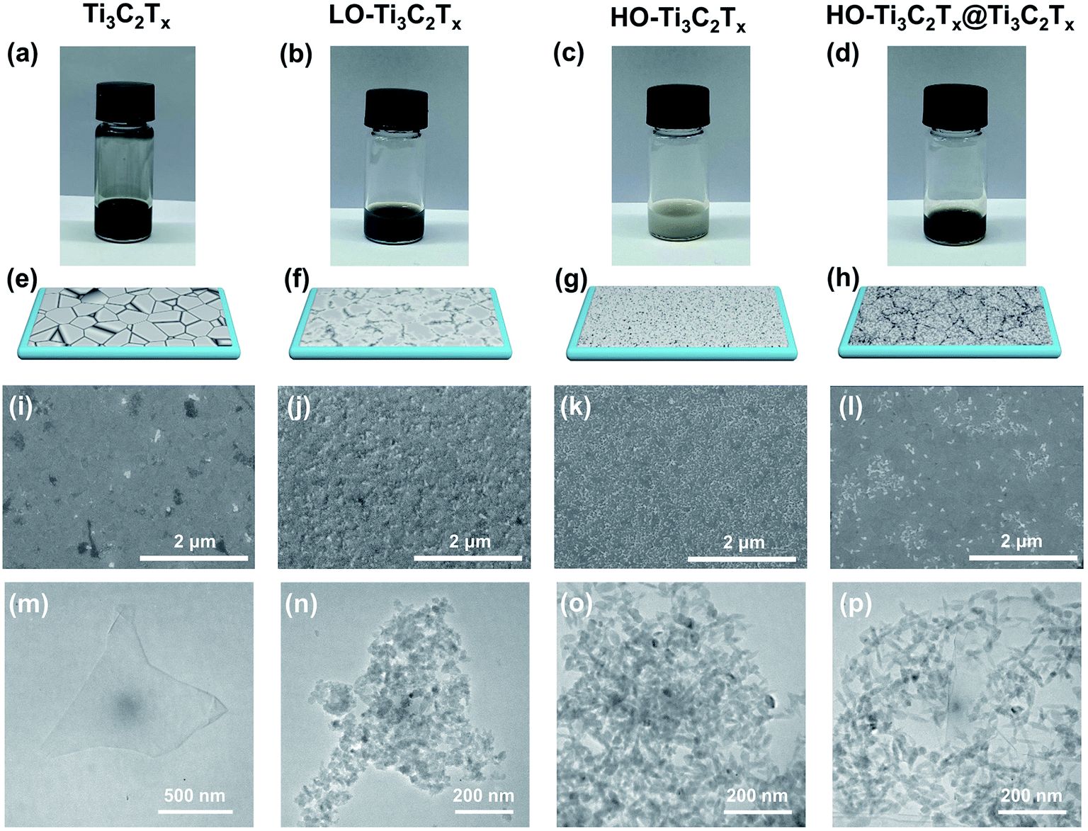 | ||
| Fig. 1 Oxidation of Ti3C2Tx MXene in solution. (a–d) Digital photos of Ti3C2Tx, LO-Ti3C2Tx, HO-Ti3C2Tx and HO-Ti3C2Tx@Ti3C2Tx hydrocolloid. (e–h) Schematic representations and (i–l) SEM images of Ti3C2Tx, LO-Ti3C2Tx, HO-Ti3C2Tx and HO-Ti3C2Tx@Ti3C2Tx films deposited on the ITO substrate by spin-coating. (m–p) TEM images of Ti3C2Tx, LO-Ti3C2Tx, HO-Ti3C2Tx and HO-Ti3C2Tx@Ti3C2Tx, respectively. | ||
To further determine the structural changes, XRD patterns and Raman spectra of these films were recorded and are shown in Fig. 2. As one can see from Fig. 2a, the most intense peak at 38.9° (2θ) of Ti3AlC2 disappeared and the (002) peak shifted from 9.5° to about 7° after 24 h etching, indicating formation of Ti3C2Tx. As the degree of oxidation increased, new peaks appeared at about 25.3° and 27.2° corresponding to anatase and rutile TiO2, respectively. The peak of Ti3C2Tx at about 7° shifted to about 6°, indicating LO-Ti3C2Tx had a wider interlayer distance according to the Bragg equation, which is assumed to be due to the oxidized nanoparticles. When Ti3C2Tx was highly oxidized (HO-Ti3C2Tx), the (002) peak disappeared, while the peaks corresponding to anatase and rutile TiO2 remained. The composites of HO-Ti3C2Tx@Ti3C2Tx showed both peaks of Ti3C2Tx and HO-Ti3C2Tx, demonstrating a good mixing. Raman spectra in Fig. 2b also exhibit the same tendency as XRD patterns. Besides, the pattern of HO-Ti3C2Tx was highly similar to that of the TiO2, proving that formed nanoparticles were TiO2. These results and UV-Vis absorption spectra (Fig. S1†) are also in agreement with the SEM and TEM images.
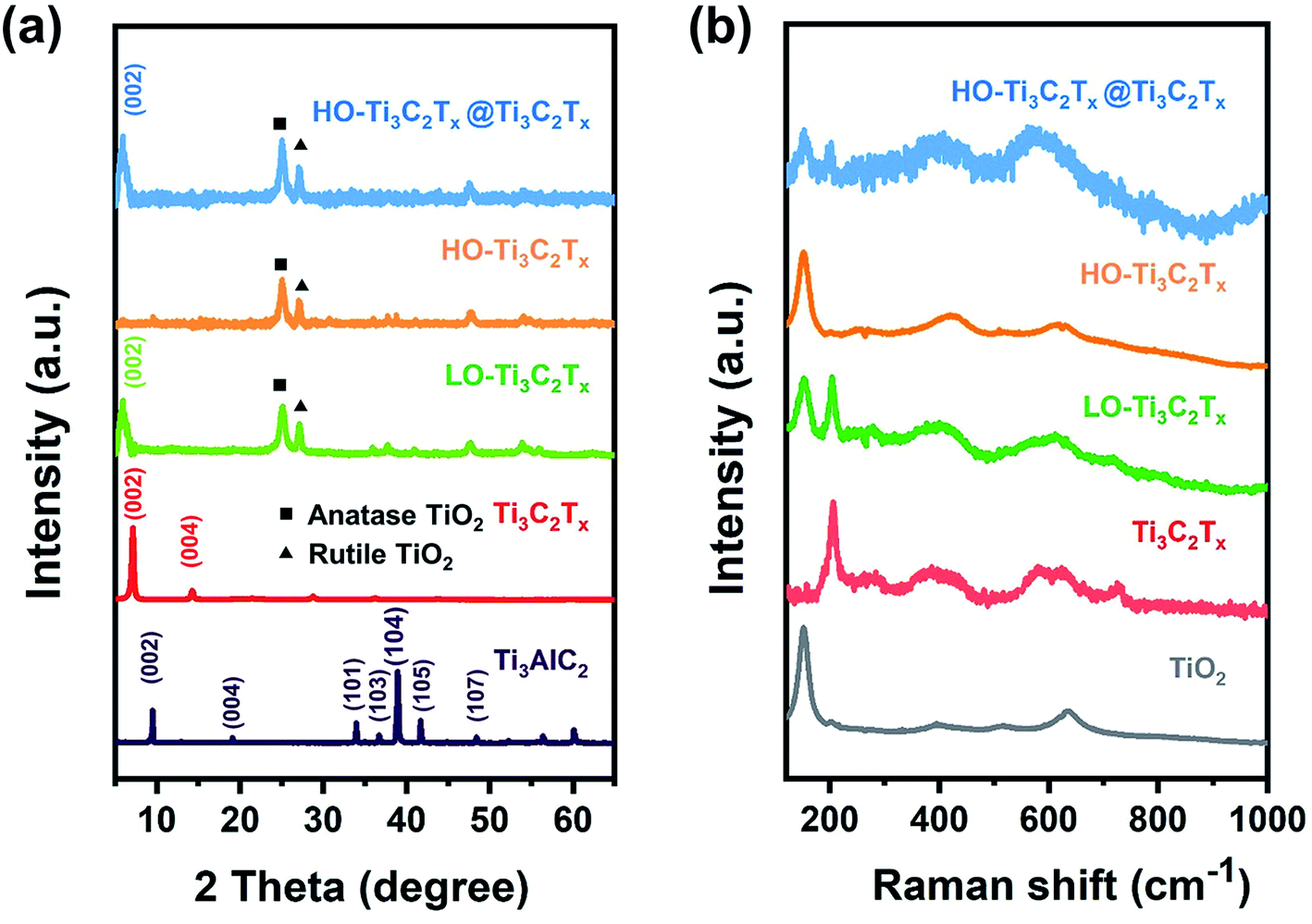 | ||
| Fig. 2 (a) XRD patterns of Ti3AlC2 powder and the dried films of Ti3C2Tx, LO-Ti3C2Tx, HO-Ti3C2Tx, HO-Ti3C2Tx@Ti3C2Tx. (b) Raman patterns of Ti3C2Tx, LO-Ti3C2Tx, HO-Ti3C2Tx, HO-Ti3C2Tx@Ti3C2Tx and TiO2 films. | ||
To get insight into the chemical changes and bonding occurring in association with the oxidation of Ti3C2Tx, XPS analysis of the samples was done, as shown in Fig. 3, S2 andS3 in the ESI.† The peaks of Ti, C, O, F were clearly detected in survey patterns, shown in Fig. S3.† And the peaks corresponding to Al were missing, confirming complete etching.40 In the high-resolution XPS spectrum of Ti 2p (Fig. 3), the doublet at 458.3 and 464.3 eV stems from Ti–O bond, while the signals marked as C–Ti–Tx 2p3/2 and C–Ti–Tx 2p1/2 at about 455 and 461 eV are from Ti–C, Ti–F and Ti–OH bonds.41 The changes of peaks suggest the transformation of surface termination groups as the oxidation progresses. By comparing the results, it could be noticed that the ratio of Ti–O bond (at 458.3 and 464.3 eV) increased when Ti3C2Tx was subjected to light oxidation, which was confirmed by the growth of TiO2 on the surface of flakes. When the Ti3C2Tx was heavily oxidized, a significant increase of Ti–O bonding was found (Fig. 3c). The spectrum of HO-Ti3C2Tx (Fig. 3c) closely matched with that of TiO2 (shown in Fig. S2†), with the Ti–O bond accounting for the main part while traces of Ti–C, Ti–F and Ti–OH were still left in HO-Ti3C2Tx. The results demonstrate that HO-Ti3C2Tx still kept a part of the original structure rather than being fully transformed into TiO2 after oxidation. The HO-Ti3C2Tx@Ti3C2Tx spectrum is shown in Fig. 3d, which looks similar to LO-Ti3C2Tx, but the ratios of Ti–O to C–Ti–Tx are different. In Fig. 3d, Ti–O bond is enhanced compared to Ti3C2Tx, indicating no loss in the Ti–O bond by any chemical interaction between the two species. Overall, the results also demonstrate the structural differences between these materials, and are in agreement with other characterization results.
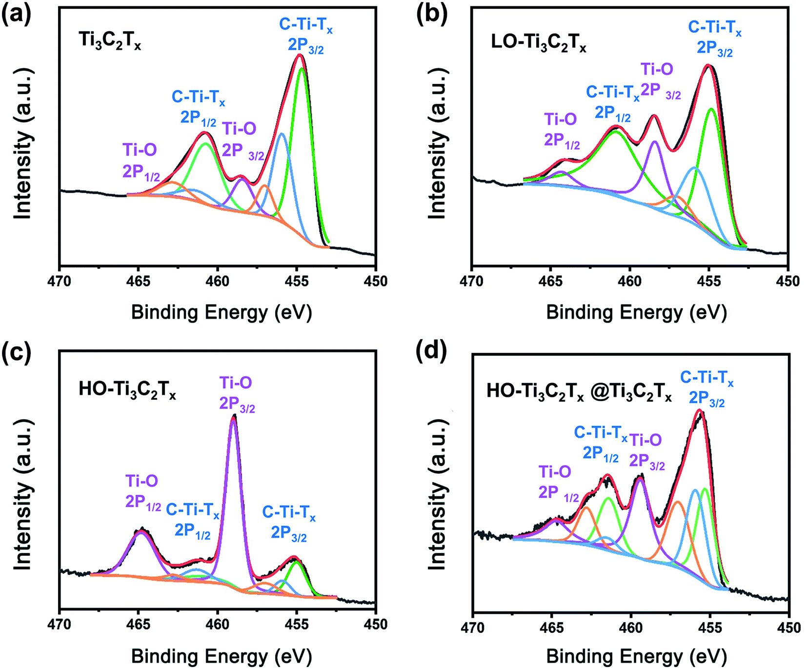 | ||
| Fig. 3 Ti 2p core level XPS spectra of the films of (a) Ti3C2Tx, (b) LO-Ti3C2Tx, (c) HO-Ti3C2Tx, and (d) HO-Ti3C2Tx@Ti3C2Tx. | ||
Photovoltaic characterization
To determine and contrast the performance of Ti3C2Tx before and after oxidation, and after mixing the two as the ETL in PSCs, the devices were fabricated with an architecture of ITO/ETL/CH3NH3PbI3/spiro-OMeTAD/Ag (Fig. 4a). The typical cross-sectional SEM image of the PSC device made with Ti3C2Tx layer as an ETL is shown in Fig. 4b, from which the thickness of ETL layer was determined to be 20 ± 3 nm. The current density–voltage (J–V) curves of PSCs based on Ti3C2Tx, LO-Ti3C2Tx, HO-Ti3C2Tx, HO-Ti3C2Tx@Ti3C2Tx and TiO2 are given in Fig. 4c and the corresponding photovoltaic parameters including Jsc, open-circuit voltage (Voc), FF, and PCE were summarized in Table 1. As the data indicates, PCE of the device based on LO-Ti3C2Tx (17.09%) was a bit higher than that of Ti3C2Tx (16.50%), which was reflected in the increase of Jsc and FF. LO-Ti3C2Tx keeps the monolayered-structure and good mobility of Ti3C2Tx while the TiO2 makes the film surface more homogenous, leading to higher Jsc and FF. When the Ti3C2Tx got heavily oxidized, the 2D structure was mostly replaced with TiO2 nanoparticles, as explained above, thus the conductivity of material was decreased, making the Jsc and FF decline. As a result, PCE of the device based on HO-Ti3C2Tx was 15.52%. Moreover, the device based on low-temperature-processed TiO2 made from isopropyl titanate was also fabricated and a PCE of 14.86% was obtained, which was in agreement with previous reports.42,43 Compared with TiO2 made from isopropyl titanate, the device based on HO-Ti3C2Tx had better Jsc and Voc due to its higher electron mobility, which will be discussed later. Besides, the J–V curves of PSCs based on HO-Ti3C2Tx@Ti3C2Tx with different volume ratios of 1:1, 5:1, 10:1 are shown in Fig. S4† and the corresponding photovoltaic performance parameters are summarized in Table S1.† As the combination of HO-Ti3C2Tx and monolayer Ti3C2Tx, the film of HO-Ti3C2Tx@Ti3C2Tx possessed high conductivity of the monolayer MXene and the semiconductor property of HO-Ti3C2Tx, which is discussed later, sourcing the increase in PCE in comparison to the devices based on Ti3C2Tx and HO-Ti3C2Tx. The best PCE of 18.29% was obtained for an optimal volume ratio of 5:1 (HO-Ti3C2Tx:Ti3C2Tx). The discussion in the following paragraphs refers to HO-Ti3C2Tx@Ti3C2Tx with 5:1 volume ratio.
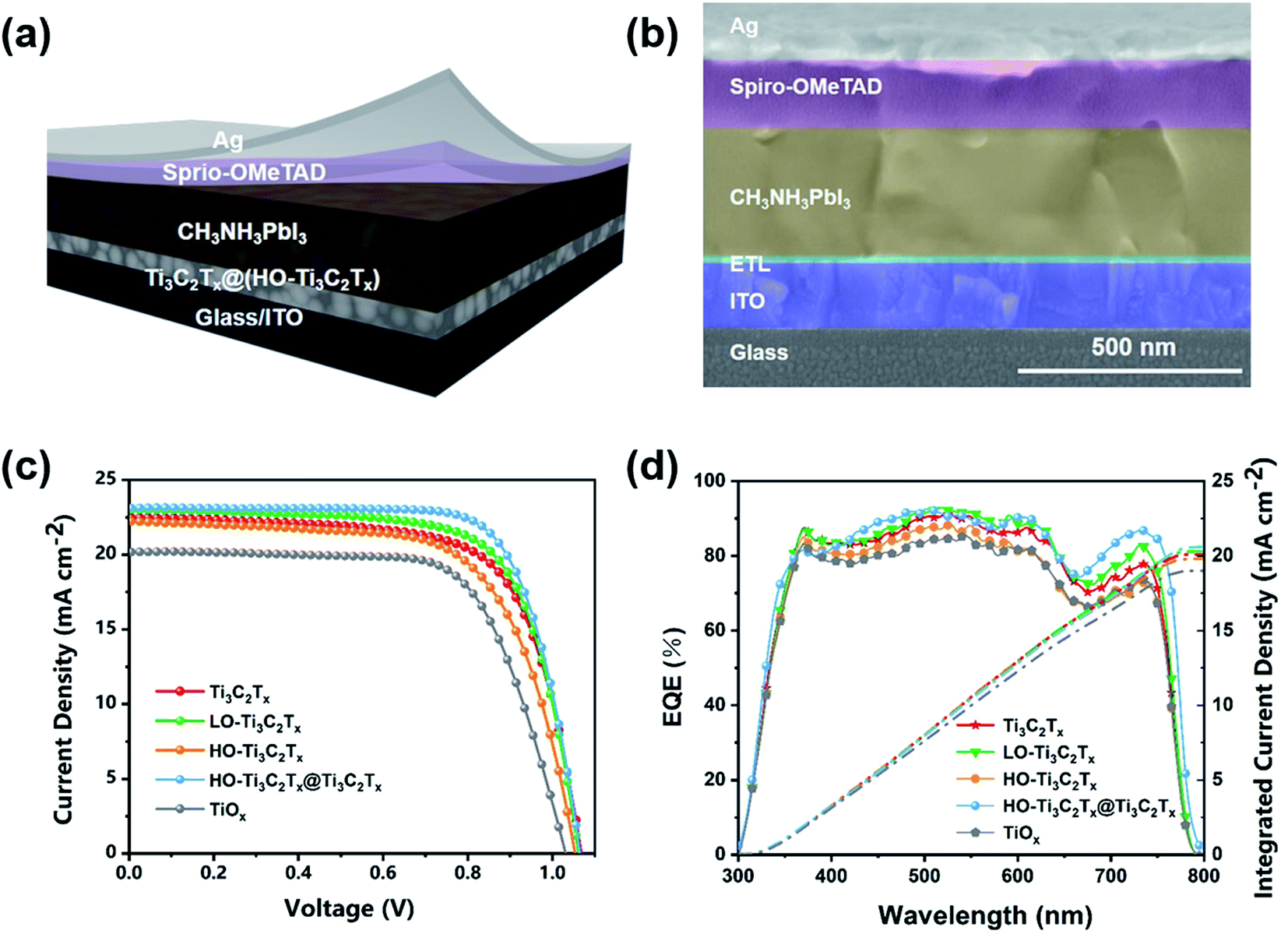 | ||
| Fig. 4 (a) Device architecture of ITO/ETL/CH3NH3PbI3/spiro-OMeTAD/Ag based on representative HO-Ti3C2Tx@Ti3C2Tx as ETL, (b) cross-sectional SEM image of the PSC device, (c) reverse scan of PSCs' J–V curves based on Ti3C2Tx, LO-Ti3C2Tx, HO-Ti3C2Tx, HO-Ti3C2Tx@Ti3C2Tx and TiO2 as ETLs under AM 1.5 G simulated illumination, and (d) their external quantum efficiency (EQE) spectra and the corresponding integrated current densities. | ||
| ETL | V oc (V) | J sc (mA cm−2) | FF (%) | PCE (%) |
|---|---|---|---|---|
| Ti3C2Tx | 1.07 | 22.35 | 69 | 16.50 |
| LO-Ti3C2Tx | 1.06 | 23.04 | 70 | 17.09 |
| HO-Ti3C2Tx | 1.06 | 22.18 | 66 | 15.52 |
| HO-Ti3C2Tx@Ti3C2Tx | 1.07 | 23.11 | 74 | 18.29 |
| TiO2 | 1.03 | 20.61 | 70 | 14.86 |
Fig. S5† shows the photovoltaic parameter statistics of (a) Voc, (b) Jsc, (c) FF and (d) PCE for the investigated PSCs based on Ti3C2Tx, LO-Ti3C2Tx, HO-Ti3C2Tx, HO-Ti3C2Tx@Ti3C2Tx and TiO2. The results have a small standard deviation and show good reproducibility of devices.
The EQE spectra (Fig. 4d) and integrated currents calculated for ETLs with Ti3C2Tx, LO-Ti3C2Tx, HO-Ti3C2Tx, HO-Ti3C2Tx@Ti3C2Tx and TiO2 (Fig. 4d) are in line with the changes in Jsc. The integrated current density from EQE curves for the device based on Ti3C2Tx was 20.10 mA cm−2. A little increase of integrated current density, which was up to 20.33 mA cm−2, was achieved with the LO-Ti3C2Tx film. That of HO-Ti3C2Tx and TiO2 were calculated to be 19.82 mA cm−2 and 18.91 mA cm−2, respectively. For the best device based on HO-Ti3C2Tx@Ti3C2Tx, the integrated current density obtained was 20.66 mA cm−2. The deviation of integrated current from EQE patterns and the actual measured Jsc values (Table 1) is about 10%, demonstrating good matching with the J–V obtained values. Moreover, the hysteresis patterns of reverse and forward scans of J–V curves are shown in Fig. S6.† The hysteresis is about 23% for the devices based on LO-Ti3C2Tx, HO-Ti3C2Tx and HO-Ti3C2Tx@Ti3C2Tx, which is less than the devices based on Ti3C2Tx (27%) in our previous work.35 On the other hand, the TiO2-based device exhibited a hysteresis of 31%. The reduced hysteresis is attributed to less surface defects and high electron mobility of the films, which promote electron transfer and prevent recombination at the ETLs/perovskite interface. Moreover, steady-state power output and current density measurements of devices based on (a) Ti3C2Tx, (b) LO-Ti3C2Tx, (c) HO-Ti3C2Tx, (d) HO-Ti3C2Tx@Ti3C2Tx and (e) TiO2 for more than 500 s were obtained (Fig. S7†). All the devices exhibited stable output power that was in good consistence with the values determined form J–V results.
To understand the changes in energy levels caused by oxidation, five model structures of Ti3C2Tx, LO-Ti3C2Tx, HO-Ti3C2Tx, HO-Ti3C2Tx@Ti3C2Tx and TiO2 were fabricated, as shown in Fig. 5. The calculations results shown in Fig. 6a suggest that Ti3C2Tx is a metallic material with the work function of about −5.35 eV, in agreement with the previously reported value.33 After light oxidation of Ti3C2Tx, LO-Ti3C2Tx still keeps the metallic properties, while the work function shifted to −6.88 eV, owing to the newly formed TiO2. This also supports the experimental results presented above, which showed TiO2 nanoparticles on the surface of flakes, which still maintained conductive MXene layers. HO-Ti3C2Tx is almost completely transformed into TiO2 and became a semiconductor whose highest occupied molecular orbital (HOMO) and lowest unoccupied molecular orbital (LUMO) are determined as −7.23 eV and −3.26 eV, respectively. After mixing with Ti3C2Tx, the energy level of HO-Ti3C2Tx@Ti3C2Tx shifted further, HOMO and LUMO were calculated to be −7.37 eV and −3.43 eV. In addition, the HOMO and LUMO of TiO2 are obtained to be −7.92 eV and −3.69 eV. Moreover, the UPS tests of HO-Ti3C2Tx, HO-Ti3C2Tx@Ti3C2Tx and TiO2 films spin-coated onto ITO substrates were also obtained as shown in Fig. S8.† The HOMO energy levels were determined by the intersection of baseline with the tangent line of the spectra and LUMO were calculated by the results of UV-vis absorption spectra, while the schematic diagram of devices' each layer based on different ETLs were summarized in Fig. 6b. Although there were some deviations in the calculated results, overall DFT results well agreed with the experimental data by showing the shift in the trends of energy level confirming the transformation from metallic to semiconductor.35,44 HO-Ti3C2Tx@Ti3C2Tx exhibits property of semiconductor and appropriate energy level to reduce recombination at the ETLs/perovskite interface, with the addition of inserted Ti3C2Tx to further increase the electron mobility. Thus, it is coherent that the device based on HO-Ti3C2Tx@Ti3C2Tx indicates the best PCE of 18.29%.
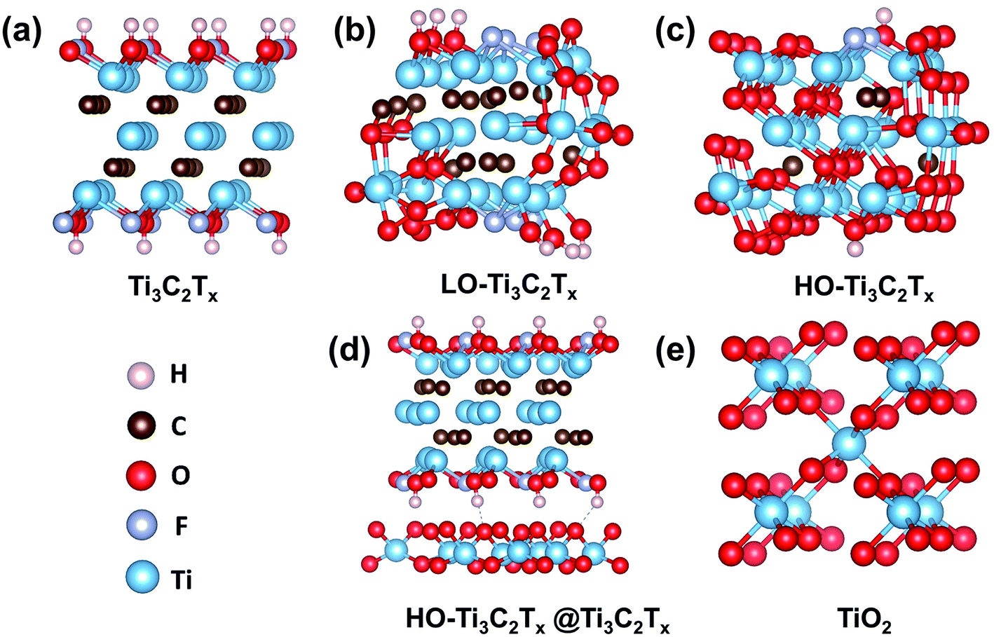 | ||
| Fig. 5 Predicted crystal structures of Ti3C2Tx, LO-Ti3C2Tx, HO-Ti3C2Tx, HO-Ti3C2Tx@Ti3C2Tx and TiO2 carried out by VASP code based on DFT. | ||
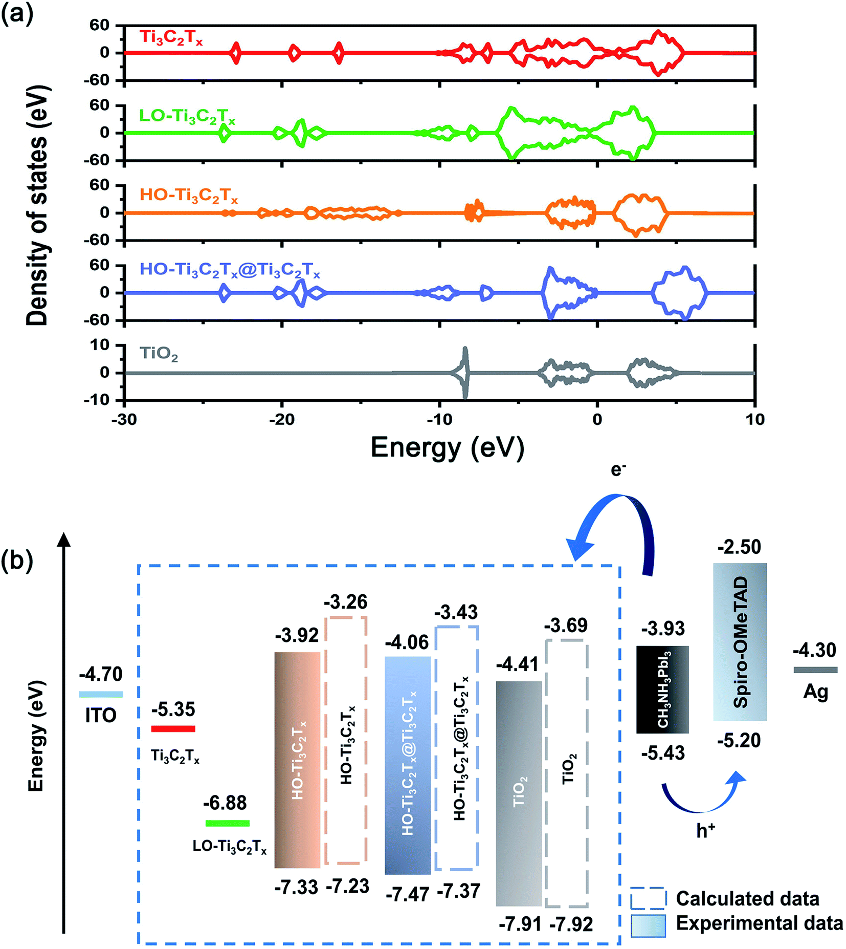 | ||
| Fig. 6 (a) Calculated density of states for Ti3C2Tx, LO-Ti3C2Tx, HO-Ti3C2Tx, HO-Ti3C2Tx@Ti3C2Tx, TiO2 and (b) schematic diagram of devices' each layer based on different ETLs determined by DFT calculation and UPS data. | ||
To investigate the electron extraction abilities of Ti3C2Tx, LO-Ti3C2Tx, HO-Ti3C2Tx, HO-Ti3C2Tx@Ti3C2Tx and TiO2, the PL spectra of the CH3NH3PbI3 perovskite layer spin-coated onto ITO/ETLs substrates were measured and shown in Fig. S9a.† The PL signal at about 780 nm is assigned to the emission from CH3NH3PbI3 (excitation at 403 nm) and its quenching is originated from electron extraction across the perovskite/ETL interface. The ITO/LO-Ti3C2Tx/perovskite sample exhibits lower PL intensity than that of ITO/Ti3C2Tx/perovskite, while ITO/HO-Ti3C2Tx/perovskite shows higher PL intensity than that of ITO/Ti3C2Tx/perovskite, indicating that low oxidation of Ti3C2Tx enhances the electron extraction and suppresses carrier recombination, but high oxidation turns out to have the opposite effect. Appropriate oxidation can make the Ti3C2Tx film exhibit semiconductor properties of TiO2 while keeping the high conductivity. On the other hand, HO-Ti3C2Tx deteriorates the monolayered-structure and shows low conductivity. Moreover, the PL intensity of ITO/TiO2/perovskite sample is higher than that of ITO/HO-Ti3C2Tx/perovskite, demonstrating that although the monolayered structure is no longer present, HO-Ti3C2Tx still shows better electron extraction than TiO2 fabricated by isopropyl titanate. Besides, the ITO/HO-Ti3C2Tx@Ti3C2Tx/perovskite exhibits the lowest PL intensity, indicating that HO-Ti3C2Tx@Ti3C2Tx offers the best electron extraction from the perovskite to the ETL among these five kinds of samples. The combination of HO-Ti3C2Tx and Ti3C2Tx effectively enhanced electron transport and suppressed carrier recombination owing to its integrated monolayered structure and suitable semiconductor property of HO-Ti3C2Tx. In addition, the TRPL spectra of perovskites based on these ETLs were shown in Fig. S9b.† The lifetimes of PL decay of Ti3C2Tx, LO-Ti3C2Tx, HO-Ti3C2Tx, HO-Ti3C2Tx@Ti3C2Tx and TiO2-based perovskites were determined as 101.1 ns, 112.3 ns, 124.5 ns, 78.2 ns and 165.7 ns, respectively. These were consistent with the PL results, further demonstrating the results of J–V curves and EQE spectra.
Electron mobility values of Ti3C2Tx, LO-Ti3C2Tx, HO-Ti3C2Tx, HO-Ti3C2Tx@Ti3C2Tx and TiO2 were tested by the method of space charge-limited current (SCLC) on the devices with the electron-only structure of ITO/SnO2/ETL/BCP/Ag under dark (Fig. S10†). The electron mobility of Ti3C2Tx, LO-Ti3C2Tx, HO-Ti3C2Tx, HO-Ti3C2Tx@Ti3C2Tx, TiO2 was determined as 1.29 × 10⁻⁵ cm2 V−1 s−1, 1.76 × 10⁻⁵ cm2 V−1 s−1, 1.30 × 10⁻⁵ cm2 V−1 s−1, 1.82 × 10⁻⁵ cm2 V−1 s−1 and 7.67 × 10⁻⁶ cm2 V−1 s−1 respectively. The device based on HO-Ti3C2Tx@Ti3C2Tx exhibited the best mobility and also yielded the best PCE. The mobility results effectively explain the improvement in Jsc and FF values in the device and accord with the results of J–V, EQE and PL.
To demonstrate whether the difference in FF is associated with interfacial charge transfer, EIS measurement was employed on devices with the structure of ITO/ETLs/CH3NH3PbI3/spiro-OMeTAD/Ag. Fig. S11† exhibits the Nyquist plots of the five devices and the equivalent circuit model that fits the experimental data with the frequency ranging from 1 MHz to 10 Hz under the standard AM 1.5 G (100 mW cm−2) simulated sunlight illumination. Besides, the fitted data is shown in Table S2.†R1 represents the series resistance associated with external wires and the ITO substrate, while the semi-circle represents the interfacial charge transfer resistance (R2) and capacitance (C) at the interface of ETLs/perovskite. R2 follows the order of TiO2> HO-Ti3C2Tx > Ti3C2Tx > LO-Ti3C2Tx > HO-Ti3C2Tx@Ti3C2Tx. The lowest R2 of 188.2 Ω is achieved by the device based on HO-Ti3C2Tx@Ti3C2Tx, indicating the highest electrons collection and the lowest charge transfer resistance at the interface, thus generating the highest FF, which is also in good accordance with J–V curves.
Besides, the stability of devices based on different ETLs was also studied and the results are shown in Fig. S12.† The devices were placed in ambient air (25 °C, relative humidity ≈ 20%) without encapsulation and tested under the standard AM 1.5 G (100 mW cm−2) simulated sunlight illumination. All the devices exhibited good stability and similar downtrend, the efficiency of TiO2-based device reduced to 64% after 800 h of storage while the other PSCs based on Ti3C2Tx and oxidized Ti3C2Tx showed better stabilities, retaining from 65% to 69% of the initial values. And, the HO-Ti3C2Tx@Ti3C2Tx-based device retained 71% of the initial PCE. Moreover, both LO-Ti3C2Tx and HO-Ti3C2Tx had good stability, demonstrating the oxidation has no negative impact on the devices' stability. The results also revealed that Ti3C2Tx had a certain passivation impact, which could decrease the chemical activity at the interface of perovskite/ETLs and suppress the hydration reaction.45 Thus, the appropriate combination of HO-Ti3C2Tx and Ti3C2Tx effectively improved the stability of devices, presenting its high potential for application in PSCs.
Conclusion
Oxidation of 2D Ti3C2Tx MXene in solution was used to produce ETLs with improved properties. Oxidation of Ti3C2Tx can reduce the defects of the film fabricated by spin-coating and generate more Ti–O bonds. The structures of oxidized Ti3C2Tx were simulated and the calculations of energy levels by the VASP code based on DFT were carried out. A transition from metal to semiconductor occurred after heavy oxidation, leading to a better matching of energy levels between ETLs and perovskite, thus rendering oxidized Ti3C2Tx more suitable as ETLs in PSCs. A PCE of 18.29% was achieved for PSCs using a composite of heavily oxidized and pristine Ti3C2Tx as ETL, in comparison with PSCs using pristine Ti3C2Tx as ETL which showed a PCE of 16.50%. The enhancement of PCE can be explained by facilitated electron transport and reduced recombination at the ETL/perovskite interface due to the reduced defects of film surface and the increase of electron mobility. This work shows that modification of MXenes can improve their performance in PSCs and other photovoltaic technologies.Author contributions
L. Y. conducted the experimental work, D. K. and Y. W. conducted theoretical calculation work, C. D., Y. D., A. J. and G. C. provided experimental instruction, B. W. provided experimental help, and X.-F. W. conceived the research idea, X.-F. W., Y. G., and T. M. guided the work. All authors contributed to the discussion of the results and edited the manuscript.Conflicts of interest
The authors declare no conflict of interest.Acknowledgements
This work was supported by the National Natural Science Foundation of China (No. 11974129 to X. F. W.) and “The Fundamental Research Funds for the Central Universities”.References
- S. D. Stranks, G. E. Eperon, G. Grancini, C. Menelaou, M. J. P. Alcocer, T. Leijtens, L. M. Herz, A. Petrozza and H. J. Snaith, Science, 2013, 342, 341–344 CrossRef CAS.
- S. Wang, Y. Jiang, E. J. Juarez-Perez, L. K. Ono and Y. Qi, Nat. Energy, 2016, 2, 16195 CrossRef.
- T. Miyasaka, Chem. Lett., 2015, 44, 720–729 CrossRef CAS.
- H. S. Kim, A. Hagfeldt and N. G. Park, Chem. Commun., 2019, 55, 1192–1200 RSC.
- A. Kojima, K. Teshima, Y. Shirai and T. Miyasaka, J. Am. Chem. Soc., 2009, 131, 6050–6051 CrossRef CAS.
- https://www.nrel.gov/pv/cell-efficiency.html .
- G. E. Eperon, V. M. Burlakov, P. Docampo, A. Goriely and H. J. Snaith, Adv. Funct. Mater., 2014, 24, 151–157 CrossRef CAS.
- Q. Jiang, Z. Chu, P. Wang, X. Yang, H. Liu, Y. Wang, Z. Yin, J. Wu, X. Zhang and J. You, Adv. Mater., 2017, 29, 1703852 CrossRef.
- N. E. Courtier, J. M. Cave, J. M. Foster, A. B. Walker and G. Richardson, Energy Environ. Sci., 2019, 12, 396–409 RSC.
- N. Li, C. Dall'Agnese, W. Zhao, S. Duan, G. Chen, S.-i. Sasaki, H. Tamiaki, Y. Sanehira, T. Miyasaka and X.-F. Wang, Mater. Chem. Front., 2019, 3, 2357–2362 RSC.
- J. N. Coleman, M. Lotya, A. O'Neill, S. D. Bergin, P. J. King, U. Khan, K. Young, A. Gaucher, S. De, R. J. Smith, I. V. Shvets, S. K. Arora, G. Stanton, H. Y. Kim, K. Lee, G. T. Kim, G. S. Duesberg, T. Hallam, J. J. Boland, J. J. Wang, J. F. Donegan, J. C. Grunlan, G. Moriarty, A. Shmeliov, R. J. Nicholls, J. M. Perkins, E. M. Grieveson, K. Theuwissen, D. W. McComb, P. D. Nellist and V. Nicolosi, Science, 2011, 331, 568–571 CrossRef CAS.
- M. Chhowalla, H. S. Shin, G. Eda, L. J. Li, K. P. Loh and H. Zhang, Nat. Chem., 2013, 5, 263–275 CrossRef.
- E. Jokar, Z. Y. Huang, S. Narra, C.-Y. Wang, V. Kattoor, C.-C. Chung and E. W.-G. Diau, Adv. Energy Mater., 2018, 8, 1701640 CrossRef.
- N. Fu, C. Huang, P. Lin, M. Zhu, T. Li, M. Ye, S. Lin, G. Zhang, J. Du, C. Liu, B. Xu, D. Wang and S. Ke, J. Mater. Chem. A, 2018, 6, 8886–8894 RSC.
- R. Singh, A. Giri, M. Pal, K. Thiyagarajan, J. Kwak, J.-J. Lee, U. Jeong and K. Cho, J. Mater. Chem. A, 2019, 7, 7151–7158 RSC.
- G. Yin, H. Zhao, J. Feng, J. Sun, J. Yan, Z. Liu, S. Lin and S. Liu, J. Mater. Chem. A, 2018, 6, 9132–9138 RSC.
- M. Naguib, M. Kurtoglu, V. Presser, J. Lu, J. Niu, M. Heon, L. Hultman, Y. Gogotsi and M. W. Barsoum, Adv. Mater., 2011, 23, 4248–4253 CrossRef CAS.
- M. Naguib, V. N. Mochalin, M. W. Barsoum and Y. Gogotsi, Adv. Mater., 2014, 26, 992–1005 CrossRef CAS.
- K. Hantanasirisakul and Y. Gogotsi, Adv. Mater., 2018, 30, e1804779 CrossRef.
- B. Akuzum, K. Maleski, B. Anasori, P. Lelyukh, N. J. Alvarez, E. C. Kumbur and Y. Gogotsi, ACS Nano, 2018, 12, 2685–2694 CrossRef CAS.
- C. J. Zhang, L. McKeon, M. P. Kremer, S. H. Park, O. Ronan, A. Seral-Ascaso, S. Barwich, C. O. Coileain, N. McEvoy, H. C. Nerl, B. Anasori, J. N. Coleman, Y. Gogotsi and V. Nicolosi, Nat. Commun., 2019, 10, 1795–1803 CrossRef.
- C. Chen, X. Xie, B. Anasori, A. Sarycheva, T. Makaryan, M. Zhao, P. Urbankowski, L. Miao, J. Jiang and Y. Gogotsi, Angew. Chem., Int. Ed., 2018, 57, 1846–1850 CrossRef CAS.
- L. Li, X. Fu, S. Chen, S. Uzun, A. S. Levitt, C. E. Shuck, W. Han and Y. Gogotsi, ACS Appl. Mater. Interfaces, 2020, 12, 15362–15369 CrossRef CAS.
- A. Iqbal, F. Shahzad, K. Hantanasirisakul, M.-K. Kim, J. Kwon, J. Hong, H. Kim, D. Kim, Y. Gogotsi and C. M. Koo, Science, 2020, 369, 446–450 CAS.
- Y. Sun, D. Jin, Y. Sun, X. Meng, Y. Gao, Y. Dall'Agnese, G. Chen and X.-F. Wang, J. Mater. Chem. A, 2018, 6, 9124–9131 RSC.
- C. J. Zhang, S. Pinilla, N. McEvoy, C. P. Cullen, B. Anasori, E. Long, S.-H. Park, A. Seral-Ascaso, A. Shmeliov, D. Krishnan, C. Morant, X. Liu, G. S. Duesberg, Y. Gogotsi and V. Nicolosi, Chem. Mater., 2017, 29, 4848–4856 CrossRef CAS.
- C. Dall'Agnese, Y. Dall'Agnese, B. Anasori, W. Sugimoto and S. Mori, New J. Chem., 2018, 42, 16446–16450 RSC.
- Z. Guo, L. Gao, Z. Xu, S. Teo, C. Zhang, Y. Kamata, S. Hayase and T. Ma, Small, 2018, 14, 1802738 CrossRef.
- L. Yang, Y. Dall'Agnese, K. Hantanasirisakul, C. E. Shuck, K. Maleski, M. Alhabeb, G. Chen, Y. Gao, Y. Sanehira, A. K. Jena, L. Shen, C. Dall'Agnese, X.-F. Wang, Y. Gogotsi and T. Miyasaka, J. Mater. Chem. A, 2019, 7, 5635–5642 RSC.
- A. Agresti, A. Pazniak, S. Pescetelli, A. Di Vito, D. Rossi, A. Pecchia, M. Auf der Maur, A. Liedl, R. Larciprete, D. V. Kuznetsov, D. Saranin and A. Di Carlo, Nat. Mater., 2019, 18, 1228–1234 CrossRef CAS.
- Z. Yu, W. Feng, W. Lu, B. Li, H. Yao, K. Zeng and J. Ouyang, J. Mater. Chem. A, 2019, 7, 11160–11169 RSC.
- L. Huang, X. Zhou, R. Xue, P. Xu, S. Wang, C. Xu, W. Zeng, Y. Xiong, H. Sang and D. Liang, Nano-Micro Lett., 2020, 12, 44 CrossRef CAS.
- T. Schultz, N. C. Frey, K. Hantanasirisakul, S. Park, S. J. May, V. B. Shenoy, Y. Gogotsi and N. Koch, Chem. Mater., 2019, 31, 6590–6597 CrossRef CAS.
- A. Di Vito, A. Pecchia, M. Auf der Maur and A. Di Carlo, Adv. Funct. Mater., 2020, 1909028 CrossRef CAS.
- L. Yang, C. Dall'Agnese, Y. Dall'Agnese, G. Chen, Y. Gao, Y. Sanehira, A. K. Jena, X. F. Wang, Y. Gogotsi and T. Miyasaka, Adv. Funct. Mater., 2019, 29, 1905694 CrossRef CAS.
- D. Wang, F. Li, R. Lian, J. Xu, D. Kan, Y. Liu, G. Chen, Y. Gogotsi and Y. Wei, ACS Nano, 2019, 13, 11078–11086 CrossRef CAS.
- B. Zheng, C. Ma, D. Li, J. Lan, Z. Zhang, X. Sun, W. Zheng, T. Yang, C. Zhu, G. Ouyang, G. Xu, X. Zhu, X. Wang and A. Pan, J. Am. Chem. Soc., 2018, 140, 11193–11197 CrossRef CAS.
- J. Wang, D. Liu, H. Huang, N. Yang, B. Yu, M. Wen, X. Wang, P. K. Chu and X. F. Yu, Angew. Chem., Int. Ed., 2018, 57, 2600–2604 CrossRef CAS.
- M. Alhabeb, K. Maleski, B. Anasori, P. Lelyukh, L. Clark, S. Sin and Y. Gogotsi, Chem. Mater., 2017, 29, 7633–7644 CrossRef CAS.
- J. Halim, M. R. Lukatskaya, K. M. Cook, J. Lu, C. R. Smith, L. A. Naslund, S. J. May, L. Hultman, Y. Gogotsi, P. Eklund and M. W. Barsoum, Chem. Mater., 2014, 26, 2374–2381 CrossRef CAS.
- J. Pang, R. G. Mendes, A. Bachmatiuk, L. Zhao, H. Q. Ta, T. Gemming, H. Liu, Z. Liu and M. H. Rummeli, Chem. Soc. Rev., 2019, 48, 72–133 RSC.
- D. Yang, R. Yang, J. Zhang, Z. Yang, S. Liu and C. Li, Energy Environ. Sci., 2015, 8, 3208–3214 RSC.
- A. Yella, L. P. Heiniger, P. Gao, M. K. Nazeeruddin and M. Gratzel, Nano Lett., 2014, 14, 2591–2596 CrossRef CAS.
- M. Li, Y. Li, S. I. Sasaki, J. Song, C. Wang, H. Tamiaki, W. Tian, G. Chen, T. Miyasaka and X. F. Wang, ChemSusChem, 2016, 9, 2862–2869 CrossRef CAS.
- X. Chen, W. Xu, N. Ding, Y. Ji, G. Pan, J. Zhu, D. Zhou, Y. Wu, C. Chen and H. Song, Adv. Funct. Mater., 2020, 30, 2003295 CrossRef CAS.
Footnote |
| † Electronic supplementary information (ESI) available: XPS analysis, J–V curves, photovoltaic parameters based on HO-Ti3C2Tx@Ti3C2Tx with different volume ratio, PL results, SCLC results, EIS fitting parameters and stability results of PSCs. See DOI: 10.1039/d0ta11397b |
| This journal is © The Royal Society of Chemistry 2021 |