Oxygen-induced defect-healing and photo-brightening of halide perovskite semiconductors: science and application

Like Huang *ab, Ziyi Ge *ac, Xiaoli Zhang d and Yuejin Zhu b
aNingbo Institute of Materials Technology and Engineering (NIMTE), Chinese Academy of Sciences (CAS), Ningbo 315201, China. E-mail: huanglike@nbu.edu.cn
bDepartment of Microelectronic Science and Engineering, School of Physical Science and Technology, Ningbo University, Zhejiang 315211, China
cCenter of Materials Science and Optoelectronics Engineering, University of Chinese Academy of Sciences, Beijing 100049, China
dSchool of Materials Science and Engineering, Zhengzhou University, Zhengzhou 450001, China. E-mail: geziyi@nimte.ac.cn

Received 10th November 2020 , Accepted 21st December 2020

First published on 21st December 2020


Abstract

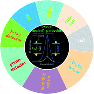
Solution-processed metal halide perovskite (MHP) semiconductors have shown remarkable success in diverse optoelectronic device applications, especially in solar cells, despite having a non-negligible density of defect states. The photoluminescence quantum yield (PLQY) is usually taken as a proxy to evaluate the optoelectronic quality of MHPs. Higher PLQYs imply a reduction of nonradiative deactivation pathways, which can contribute to a lower nonradiative voltage loss and higher open circuit voltage of the final device. Many studies have reported various methods to passivate the defect states in MHPs and to enhance their PLQYs. An interesting observation that has been repeatedly reported recently is a drastic PLQY enhancement upon exposure of MHPs to dry air or oxygen under illumination, which is the so-called photo-brightening phenomenon associated with oxygen-induced defect-healing (OIDH) of MHPs. This phenomenon involves the interaction between oxygen and defects in MHPs, as the adsorption and diffusion of oxygen can mediate the perovskite lattice and passivate the defects (such as halogen vacancies and interstitials, halogen migration and aggregation) on the surface or in the bulk of MHPs. In this review, we mainly focus on the recent advances and the related sciences in enhancing the optoelectronic quality of emerging MHP semiconductors by effective defect passivation though a facile oxygen post-treatment, which is the so called OIDH effect and the associated photo-brightening effect, as well as their wide applications in solar cells, LEDs, oxygen/ozone sensors, X-ray detectors, etc. Our work highlights the great potential of the efficient and convenient in situ defect passivation of emerging MHP semiconductors by oxygen (abundant in an ambient atmosphere) towards various perovskite based optoelectronic applications.


Like Huang received his M.S. degree in solid state electronic physics from Ningbo University and PhD degree in electronic science and technology from Nankai University. He conducted his postdoctoral research on perovskite solar cells at the Ningbo Institute of Materials Technology and Engineering, Chinese Academy of Science. Then he moved to Ningbo University as an associate professor. His research interests focus on photovoltaic materials and solar cell device physics.

Ziyi Ge got a PhD from the Institute of Chemistry, Chinese Academy of Sciences. He conducted his postdoctoral research on organic electronics at the Tokyo Institute of Technology, Kanagawa University, Japan and the University of New South Wales, Australia. Currently, he is the leader of the Organic Electronic Material and Device Group at the Ningbo Institute of Material Technology and Engineering, Chinese Academy of Sciences. His research interests focus on OLEDs, organic solar cells, and the related materials.

Xiaoli Zhang obtained her PhD in materials chemistry from Pukyong National University. Then, she worked as a research fellow at Monash University and the University of Melbourne. She commenced her vice-chancellor's research fellowship at the University of New South Wales (2012–2015) and then worked at the University College London (2014–2015), before taking a full faculty position at Zhengzhou University in 2016. She won the Marie Sklodowska-Curie Actions Seal of Excellence Award from the European Commission Horizon 2020 research and innovation funding programme.

Yuejin Zhu is a professor in the Department of Microelectronic Science and Engineering, School of Physical Science and Technology, Ningbo University. He got his PhD from the Department of Physics, Nanjing University. He is now a member of the steering committee of physics major in Zhejiang province and a doctoral supervisor. He is mainly engaged in the research of semiconductor materials and devices. He has published more than 150 papers in Adv. Energy Mater., ACS Nano, Phys. Rev. B and other famous international academic journals, and has obtained 16 invention patents.


1 Introduction

With excellent optoelectronic properties and simple solution processing, metal halide perovskites (MHPs), as excellent emerging semiconductors, have shown great potential in various optoelectronic applications in the last decade, especially in the photovoltaic field. The power conversion efficiency (PCE) of single-junction perovskite solar cells (PSCs) has rapidly increased from initial 3.8% (ref. 1) to a certified value of 25.2% (ref. 2) presently. However, whilst great strides have been made in photovoltaic performance, our understanding of the fundamental properties of these materials is still incomplete.3 Especially, this achievement is fulfilled mainly based on solution processed polycrystalline perovskite films with inevitable defects, which is usually adopted as the absorption layer.4

To further increase the PCE of PSCs, it is important to further reduce the unavoidable defects in polycrystalline perovskite films, including surface, grain boundary and bulk defects, which are very sensitive to the film fabrication process.5,6 To date, many passivation strategies have been reported to reduce the charge trap density present in perovskite films, such as the introduction of functional molecules (such as PbI2, MACl, FACl, and PEAI), metal ions (such as Li+, K+, Rb+, and Cs+), and halogen ions into the bulk or onto the surface of perovskite films.6 For example, an organic halide salt, PEAI, was recently introduced as an effective additive layer for surface defect passivation of perovskites, and a certified efficiency of 23.32% was once obtained.7Fig. 1A presents the common imperfections in perovskite films and their passivation by ionic bonding, coordinate bonding, and conversion to wide band gap materials, and suppression of ion migration at extended defects.8Fig. 1B shows the experimentally determined energy levels associated with defects in MAPbI3 and determined by different techniques.9 These structural defects can introduce different trap levels in the band gap of MHPs, which may have a varying degree of influence on the final device performance. Therefore, effective passivation measures are urgently needed to remove these defects and to further improve the device performance.


image file: d0ta10946k-f1.tif
Fig. 1 (A) Imperfections in a perovskite film and their passivation by ionic bonding, coordinate bonding, and conversion to wide band gap materials, and suppression of ion migration at extended defects. Reprinted with permission from ref. 8. Copyright 2019 Royal Society of Chemistry. (B) Experimentally determined defect levels in MAPbI3 (by different techniques). Reprinted with permission from ref. 9. Copyright 2018 Nature Publishing Group. (C) Passivation by a Lewis base. Proposed passivation mechanism of thiophene or pyridine (a). Reprinted with permission from ref. 10. Copyright 2014 American Chemical Society. Schematic diagram of PLQY enhancement (b). Reprinted with permission from ref. 11. Copyright 2016 American Chemical Society. Schematic illustration of the D4TBP passivation effect on defect sites (c). Reprinted with permission from ref. 12. Copyright 2019 American Chemical Society. (D) Histogram of published studies on the experimentally assigned types of defects in perovskites employing passivation strategies. Reprinted with permission from ref. 7. Copyright 2019 Wiley-VCH.

In addition to the above-mentioned defect passivators, Lewis acids and bases are a class of substances that have a particular effect on the specific defects of perovskites.10 Generally, a Lewis acid refers to a molecule or ion that accepts a foreign electron pair, while a Lewis base represents a molecule or ion that gives an electron pair. Such molecules could combine with perovskites via covalent bonds to form acid–base complexes without electron transfer. Consequently, Lewis acids have unique passivation capabilities for defects with lone pairs of electrons like free iodide ions and lead iodine antiside defects; electron-deficient defects such as Pb2+ interstitials can be strongly bonded by Lewis bases. Deep-level trap recombination centers induced by anion and cation defects can be well eliminated, and the overall device performance can be significantly improved. For example, Snaith et al. have increased the efficiency of solution-processed planar heterojunction perovskite solar cells from 13% to 15.3% and 16.5% using Lewis bases thiophene and pyridine treatments, respectively (Fig. 1C(a)).10 The increase in the PL lifetime close to an order of magnitude demonstrated that thiophene and pyridine have good passivation effects on defects, which stems from the fact that these Lewis base molecules can bind to the under-coordinated Pb ions in the perovskite crystal. Ginger et al. observed photoluminescence lifetimes exceeding 8 μs and a photoluminescence quantum yield (PLQY) exceeding 30% in polycrystalline films by a variety of Lewis base treatments on MAPbI3 films (Fig. 1C(b)).11 Yang et al. synthesized a new molecule D-4-tert-butylphenylalanine (D4TBP) with 4-tert-butylphenyl, amine, and carboxyl, which has a very significant passivation effect on Lewis acid defects (Fig. 1C(c)).12 The passivation ensures an extremely small open-circuit voltage (Voc) loss of only 0.34 V in PSCs, which is the lowest value reported in the literature.

Apart from these organic molecule-based Lewis acids/bases that can function as defect passivators, other simple small molecules or ions, such as O2, O3, H2O, H2O2, O, O2− and Cl, may also serve as efficient defect passivators to enhance the optoelectronic quality of perovskite films and crystals towards various applications. Especially, oxygen, abundant in the ambient atmosphere, has been reported to serve as an efficient and convenient in situ defect passivator during the deposition of inorganic MHP semiconductor films.13Fig. 1D provides a comprehensive list of the types of defects that are important to be considered and eliminated for solar cell applications, wherein the halogen vacancy defect gets the most attention.7 Below we will see the interplay between oxygen and the halogen vacancy that has a significant influence on the optoelectronic properties and thus the device performance.

For actual optoelectronic application of perovskites, the effect of ambient O2 is an important issue that should be addressed. In classical inorganic semiconductor materials, the effect of oxygen on the material properties and thus device performance has been widely reported. For instance, Ding et al. revealed the influences of oxygen passivation of silicon nanocrystals on their trap states, electron mobility, and hybrid solar cell performance.13 It is found that controlled particle oxidization can efficiently reduce carrier traps and improve electron mobility, while excessive oxidation can introduce an oxygen rich layer on the particle surface blocking carrier transport and deteriorating electrical properties inversely (Fig. S1A). Zhang et al. found that in-gap states (IGSs) near the valence band occur frequently in artificial semiconductor quantum dots (QDs) except when treated with reducing agents (such as hydrazine).14 By virtue of experimental and theoretical study, they revealed that the oxygen molecule is most likely the origin of these IGSs. They further expect these impurity-induced deep in-gap states to be a common occurrence in ionic semiconductors, where the intrinsic vacancy defects either do not produce IGSs or produce shallow states near band edges. Tang et al. reported that oxygen addition during Sb2Se3 film evaporation significantly improves the CdS/Sb2Se3 heterojunction quality through effective passivation of interfacial defect states, which results in a substantial enhancement in device performance (Fig. S1B).15 Schwermann et al. proposed the incorporation of oxygen atoms as a mechanism for photoluminescence enhancement of chemically treated MoS2 (Fig. S1C).16 Nan et al. also reported strong photoluminescence enhancement of MoS2 through defect engineering and oxygen bonding (Fig. S1D).17 These studies confirm the vital role of oxygen as an efficient and universal defect passivator of various classical semiconductors, which implies the great potential of oxygen induced defect passivation in halide perovskites as emerging new semiconductors.

Recently, experimental and theoretical research about the contradictory and controversial effect of O2 on hybrid perovskites has attracted increasing attention with several research groups noting that O2 can also affect the performance of PSCs.18–20 In fact, theoretical calculations have demonstrated that oxygen atoms can effectively passivate traps in MHPs and occupy halogen vacancies, thus suppressing halogen redistribution and phase separation. Within this review, we take a bird's-eye view of the recent advance in the understanding of the effect of oxygen on hybrid perovskite properties and perovskite-based device performance, with applications in PSCs, PLEDs, etc. as typical examples.

2 Oxygen annealing process in PSCs: phenomenon and experience in early research

Perovskites have shown great success in various optoelectronic applications, especially in the photovoltaic field, though with various defects that cannot be ignored. There have been many review articles published on defects and their passivation in the past decade as mentioned, and here we will mainly focus on the oxygen-induced defect-healing effect of perovskites.

In early studies, the “missing” Cl and its role in improving the optoelectronic properties of Cl-included perovskites has once been the focus of intensive study. Delugas and coworkers revealed the defect role of Cl in MAPbI3 perovskites with Cl inclusion.21 In their work, methyl-ammonium fragmentation in amines is confirmed as a source of localized trap levels in the band gap, while an amount of 2% additional interstitial Cl is capable of removing these localized defect states. Polycrystalline MAPbI3 perovskite shows complex optoelectronic behavior, largely because its 3D semiconducting inorganic framework is strongly perturbed by the organic cations and ubiquitous structural or chemical inhomogeneity. Based on a newly developed time-dependent DFT formalism, Beljonne et al. found that lead and iodine vacancies can yield deep trap states that can be healed by dynamic effects (rotation of the methyl-ammonium cations in response to point charges), or through slight changes in chemical composition, for example, by introducing a tiny amount of Cl dopant into the defective MAPbI3 (Fig. S2).22 This is supported by the enhanced PL intensity and lifetime of MAPbI3−xClx with increasing Cl content (x). By DFT calculations, Yin et al. suggested that Cl and O can spontaneously segregate into grain boundaries (GBs) and passivate those defect levels and deactivate the trap state, implying a similar role of electronegative Cl and O as electron acceptors in passivating the defects in MHPs.27 This work laid the theoretical foundation for oxygen as an effective passivator for MHPs.

The photoluminescence quantum yield (PLQY) is usually taken as a proxy to evaluate the optoelectronic quality of lead halide perovskites. Higher PLQYs imply a reduction of non-radiative deactivation pathways, which can contribute to a lower non-radiative voltage loss and higher Voc. Apart from the above-mentioned thermodynamics or chloride dominant self-induced defect-healing,23–26 published studies have reported many other methods to passivate the defect states in perovskites and to enhance their PLQYs. An interesting observation that has been repeatedly reported is a drastic PLQY enhancement upon exposure of prototypical lead halide perovskites to dry air or oxygen under illumination, which is the so-called photo-brightening phenomenon associated with oxygen-induced defect-healing of perovskites. This confirms the correct foresight of the theoretical work of Yin et al. as mentioned above.

In fact, in early research, there have been reports about oxygen annealing perovskites to improve the device performance, while the mechanism behind is not clear. Ren et al. revealed the effect of post-atmosphere treatment on the performance of MAPbI3-based n–i–p planar PSCs.28 It is found that annealing MAPbI3 in O2 (placing the films in dry O2 at 65 °C prior to electrode deposition) can lead to a substantial increase in the PCEs of the devices. Also, strong dependence on the annealing temperature for the PCEs of the devices suggests that a thermally activated process may underlie the observed phenomenon (Fig. 2A(a)). It is believed that the annealing process may facilitate the diffusion of O2 into spiro-MeOTAD for inducing p-type doping of the hole transport material, which enhances its conductivity (Fig. 2A(b)). Furthermore, the process can decrease the localized state density at the GBs as well as the bulk of perovskite. Utilizing thermal assisted O2 annealing, highly efficient devices with good reproducibility can be achieved. Their results suggest that the improvement in device performance by the O2 annealing process is due to the reduction in the defect density of the perovskite film as well as the enhancement in the conductivity of spiro-MeOTAD. This work highlights the critical role of post-O2 annealing treatments in enhancing the device performance and reproducibility.


image file: d0ta10946k-f2.tif
Fig. 2 (A) Effect of thermal-oxygen annealing: transient PL spectrum of the perovskite film with or without O2 post-annealing treatment (a). The resistance of the spiro-MeOTAD film with and without O2 post-annealing (b). Reprinted with permission from ref. 28. Copyright 2014 Nature Publishing Group. (B) Atmospheric influence upon the crystallization, electronic and photophysical properties of the perovskite: steady-state (a) and time-resolved (b) PL spectra, absorption spectra (c) and PDS spectra (d) of MAPbI3−xClx films prepared under nitrogen and ambient conditions for different annealing times and temperatures. Reprinted with permission from ref. 29. Copyright 2015 American Chemical Society.

Snaith et al. investigated the atmospheric influence upon crystallization and electronic disorder and its impact on the photophysical properties of MAPbI3−xClx films as well as the final device performance (Fig. 2B).29 It was found that the crystal formation and photophysical properties of MAPbI3−xClx films are kinetically driven by the annealing atmosphere, time and temperature. Generally, annealing in air produces an improved crystallinity and large grain domains as compared to nitrogen. Lower photoluminescence quantum efficiency (PLQE) and shorter photoluminescence (PL) lifetimes are observed for nitrogen annealed perovskite films as compared to their air-annealed counterparts (Fig. 2B(a and b)). The air annealed perovskite films show higher absorption in the visible region than the nitrogen-annealed one, a trend that is surprisingly reversed in the near-IR region (Fig. 2B(c and d)). This indicates that a change in crystal symmetry is partially responsible for the observed red shift in PL emission and is not exclusively due to the energy relaxation. A higher degree of crystal disorder could lead to lower PLQEs, PL lifetimes and higher recombination in nitrogen-annealed samples. Photothermal deflection spectroscopy (PDS) suggests that air annealed films exhibit a remarkably lower level of disorder than the nitrogen annealed one. Janssen et al. reported the complex effect of oxygen on the efficiency of planar p–i–n metal PSCs with a PEDOT:PSS hole transport layer.30 It is shown that processing of a perovskite layer on top of PEDOT:PSS via spin coating of a precursor solution chemically reduces the oxidation state of PEDOT:PSS. This reduction leads to a lowering of the work function of PEDOT:PSS and the perovskite layer on top of it. As a consequence, the solar cells display inferior performance. The reduced PEDOT:PSS can be re-oxidized by thermal annealing of the PEDOT:PSS/perovskite layer stack in the presence of oxygen. As a consequence, thermal annealing of the perovskite layer in air provides PSCs with increased performance.

These early results suggest that oxygen has a significant effect on the properties of perovskite materials and device performance thereof, but the underlying mechanism is not clear.

3 Oxygen–perovskite interaction and its effects

3.1 Oxygen–perovskite interaction: adsorption, diffusion, binding and reaction

Since the above-mentioned reports on oxygen annealing to improve the device performance, the mechanism behind such a phenomenon has attracted researchers' attention. The effect of oxygen adsorption and diffusion on the structure, stability, electronic structure and properties of perovskites has been comprehensively studied by combined experiments and theoretical calculations.

As for the effect of oxygen adsorption and diffusion, Grancini et al. revealed the surface photo-physics of MAPbI3 single crystals (SCs) and their interaction with the environment.31 They found that water molecules can permeate across the perovskite structure to form a partly hydrated phase, occurring spontaneously due to hydrogen bonding interactions with the perovskite lattice, as the formation energy of 4MAPbI3·H2O is negative (−0.45 eV) indicating spontaneous water incorporation into the perovskite lattice, while the incorporation of oxygen molecules is unfavorable, with a positive formation energy of 0.17 eV. This implies that the oxygen diffusion in the perfect single crystal is not fast.

As for the effect of oxygen binding and reaction, Hao et al. revealed the synergistic effects of water and oxygen molecule co-adsorption on the (001) surfaces of tetragonal MAPbI3 using DFT calculations to uncover the possible effect of oxygen on the degradation process of MAPbI3.32Fig. 3A shows the possible adsorption sites for water molecule or oxygen molecule coadsorption. They found that oxygen molecules have strong interactions with the (001) surfaces of tetragonal MAPbI3 through the formation of a chemical Pb–O bond on the PbI2-terminated surface and a hydrogen bond on the MAI-terminated surface. The adsorbed oxygen molecules introduce empty states near the Fermi level of the surfaces, which can facilitate charge transfer between the surface and oxygen molecules (Fig. 3B). Furthermore, when an oxygen molecule is located atop a Pb atom on the PbI2-terminated surface, the calculated adsorption energies indicate that the surface is more attractive to water molecules, making the surface even more sensitive to humidity. These results suggest that oxygen molecules play an important role in the initial stage of the degradation of perovskite materials.


image file: d0ta10946k-f3.tif
Fig. 3 (A) Possible adsorption sites for oxygen molecules. (B) Geometric structures and pDOS of an oxygen molecule at different sites on surfaces. Reprinted with permission from ref. 32. Copyright 2016 American Chemical Society. (C) Raman spectra of pristine and PbO-like MAPbI3. Reprinted with permission from ref. 33. Copyright 2016 American Chemical Society. (D) Size comparison of superoxide and iodide anions. (E) Oxygen-induced photo-degradation. (F) Oxygen diffusion pathways and associated degradation regions. (a) O2 diffusion in inter-particle regions and the initial reaction with particle surfaces on a timescale of hours leading to reduction in device efficiency, Voc and photocurrent and (b) O2 diffusion into bulk regions on a time scale of days leading to a phase change from the photo-absorbing perovskite phase into the non-absorbing lead iodide phase (yellow). Reprinted with permission from ref. 35. Copyright 2017 The Author(s).

In another relevant study by Kong et al., resonance Raman spectroscopy is combined with surface and bulk crystal characterization to interpret the oxygen intercalation phenomenon on the surface of MAPbI3 (Fig. 3C).33 It is found that oxygen can intercalate into the frameworks of MAPbI3 with the assistance of laser excitation. By lowering down the pressure in the experimental chamber, the intercalated oxygen can be readily removed. XPS and XRD characterization results suggest that Pb–O bonds are mainly formed on the surface of MAPbI3 but are constrained to avoid the formation of the PbO compound. DFT calculation supports the above conclusions. PL characterization shows that the intercalation of oxygen into MAPbI3 results in evident luminescence quenching. Thus, the oxygen intercalation on the surface of MAPbI3 could potentially be used as an oxygen sensor with high sensitivity and repeatability. In the work by Zhang et al., the interactions between the MAI-terminated MAPbI3 (110) surface and O2 molecules in the presence of excess mobile electrons were studied by DFT calculations.34 Their results show that molecular O2 only weakly interacts with the perovskite surface. However, a superoxide, which is formed from the reaction between an oxygen molecule and an excess electron, reacts readily with the perovskite surface by forming a Pb–O covalent bond with a surface Pb ion. By further introducing an excess electron, the superoxide is converted into a peroxide and the two O atoms form two covalent bonds with the surface Pb in a side-on configuration. During these processes, the local Pb–I octahedral structure disintegrates. The formation of the P–O covalent bonds can be the precursor of the PbO in the degradation products.

Although oxygen only weakly interacts with the perovskite surface and has a positive binding energy with the single crystal perovskite lattice, as mentioned above, the perovskite films in actual solar cells are mostly polycrystalline. Oxygen molecules may diffuse rapidly through the loose grain boundary zone. Haque et al. reported that fast oxygen diffusion and iodide defects mediate the oxygen-induced photo-degradation of PSCs (Fig. 3D–F).35 In fact, oxygen diffusion into perovskite polycrystalline films is observed to occur remarkably fast with, for example, a typical film (500 nm thick) reaching complete saturation within 10 min (Fig. 3F). It is shown that the fast oxygen diffusion into MAPbI3 films is accompanied by photo-induced formation of highly reactive superoxide species and iodide vacancies are the preferred sites in mediating the photo-induced formation of superoxide species from oxygen (Fig. 3E), as superoxide species have a smaller size than iodide ions. Also, MAPbI3 polycrystalline films composed of smaller crystal grains show a higher yield of superoxide generation and a higher degradation rate than MAPbI3(Cl) films with larger grains, suggesting a direct correlation between the yield of superoxide generation (and subsequently degradation rate) and perovskite crystal size and thus grain boundary density. These results suggest that oxygen diffuses rapidly in the polycrystalline perovskite with the aid of halogen vacancies and grain boundaries.

3.2 Effects of oxygen–perovskite interaction on the electronic structures and electrical properties of MHPs

Surface oxygen adsorption and bulk oxygen diffusion may lead to changes in the electronic structure and electrical properties of perovskites.36 As for the electronic structure, Koch et al. addressed the effect of water, oxygen, and air exposure on MAPbI3−xClx perovskite surface electronic properties by a comprehensive photoelectron spectroscopy (PES) study.37 It is shown that pure oxygen exposure reduces the typically observed pronounced n-type surface character (Fig. S3A), while pure water exposure increases it. A very low water partial pressure, e.g., as encountered in inert-gas glove boxes and in a high vacuum of 10−6 mbar, reduces the perovskite work function due to water physisorption, which is fully reversible upon mild annealing (room temperature to 50 °C) in an ultrahigh vacuum. Upon exposure to ambient air, the effect of oxygen prevails over that of water, and the perovskite becomes less n-type as seen by a 0.6 eV Fermi level shift toward the mid-gap. The results help in understanding variations of the surface electronic properties reported for perovskites, which in turn impact the energy level alignment at heterojunctions in devices.

For electrical properties, Cahen et al. tracked the electronic processes in MAPbI3(Cl) films in vacuo, and in N2, air, and O2, using impedance spectroscopy (IS), contact potential difference (CPD), and surface photovoltage measurements, which provides direct evidence for perovskite sensitivity to the ambient environment (Fig. S3B).38 A 2-orders of magnitude decrease in the film resistance upon transferring the film from an O2-rich ambient atmosphere to vacuum was observed (Fig. S3B(b and c)). The same change under ambient conditions also results in a 0.5 V decrease in the material work function. These results suggest that facile adsorption of oxygen onto the film dedopes it from n-type semiconductor to intrinsic semiconductor. While appearance of negative capacitance in vacuo or post vacuo N2 exposure, indicates for the first time an electrochemical process in the perovskite (Fig. S3B(d and e)). These effects influence any material characterization, i.e., results may be ambient-dependent due to changes in the material's electrical properties and electrochemical reactivity, which can also affect material stability. These results stress the crucial importance of stringent environment control during perovskite material characterization in future studies.

The above-mentioned studies have pointed out that oxygen adsorption on the surface will lead to the change of the electronic structure and energy level of perovskites, but the theoretical blueprint of the specific mechanism behind it is still not clear.

4 Oxygen-induced defect-healing (OIDH) and photo-brightening of MHPs

The interaction between oxygen and the perovskite can not only affect the structure, stability and energy levels, but also interact with the surface and/or bulk defects of the perovskite as it adsorbs on the surface and further invades into the bulk phase of polycrystalline perovskite films, thus passivating defects on the surface, at the grain boundary and in the bulk phase and improving the PLQY. Especially, fast O2 diffusion into MAPbI3 has been proven and found to be mediated by defects as mentioned above.35 The PLQY is usually taken as a proxy to evaluate the optoelectronic quality of halide perovskites. Higher PLQYs imply a reduction of non-radiative deactivation pathways, with long-lived and long-transported charge carriers allowing efficient charge collection at selective contacts. An interesting observation that has been repeatedly reported is a drastic PLQY enhancement upon exposure of halide perovskites to dry air or oxygen. This observation indicates that controlled exposure to oxygen or mild oxidants could lead to trap annihilation and improved solar cell performance. Interestingly, the effect can be reversible over a few cycles, which further suggests that the mechanism underlying such a behavior should be related to a fairly weak chemical interaction between O2 and the perovskite. Impedance spectroscopy results also suggested a reversible effect of oxygen on MAPbI3 electronic properties, associated with a dedoping of the material. It was also proposed that the effect of light and oxygen adsorption can significantly reduce the density of these trap states in MAPbI3. Thus, parasitic non-radiative charge carrier losses can be eliminated and the PLQY can be improved.

4.1 Oxygen-induced defect-healing effect at the grain boundaries of MHPs

The mechanism of oxygen passivation of defect states at the grain boundary was first reported compared with the surface and bulk. In 2015, inspired by an early study of the Cl-induced passivation effect of defects at CdTe grain boundaries, Yin et al. reported the passivation effect of Cl and O at the GBs of MAPbI3 by DFT calculations (Fig. 4), considering different I positions as Cl/O substitution sites.27 They found that the spontaneous segregation of extrinsic elements such as Cl and O can weaken the wrong bond at GBs and thus reduce the shallow trap state with a level close to the valence band maximum (VBM). As the GB state can increase the hole effective mass and act as a shallow trap state which hinders the hole diffusion, oxygen passivation of GBs may enhance the device performance of polycrystalline perovskite based solar cells. Their theoretical results provide a fundamental understanding of the oxygen passivation mechanism at perovskite GBs. However, the work does not mention any experimental observations that oxygen passivation of GB defects could improve the luminescence of the perovskite.
image file: d0ta10946k-f4.tif
Fig. 4 (A) Different I positions considered as Cl/O substitution sites in MAPbI3 Σ5(310) GBs. (B) The relative total energies when Cl/O substitutes on different I sites in (A). The unsymmetrical behavior is attributed to the random orientations of the CH3NH3 molecule. (C) Total DOS and partial DOS at wrong bonds of unpassivated, Cl-passivated and O-passivated MAPbI3 Σ5(310) GBs. Reprinted with permission from ref. 27. Copyright 2015 Wiley-VCH.

4.2 Oxygen-induced defect-healing effect on the surface and in the bulk phase of MHPs

4.2.1 Impact of the atmosphere on the luminescence properties of MHPs. As for the impact of the atmosphere, in 2015, Galisteo-López et al. reported the environmental effects on the photophysical properties of MAPbI3(Cl).39 They demonstrated that the luminescence properties of MAPbI3(Cl) are determined by the interplay between photoinduced activation and darkening processes, which strongly depend on the atmosphere surrounding the samples. They have isolated oxygen and moisture as the key elements in each process, activation and darkening, both of which involve an interaction with photogenerated carriers. These findings show that environmental factors play a key role in the performance of lead halide perovskites as efficient luminescent materials. From the results of Fig. 5A, it is evident that the strong photo-darkening is mainly due to the presence of moisture in the atmosphere surrounding the samples when the sample is illuminated in air. Furthermore, from the results in Fig. 5B, it can be seen that the photo-darkening during illumination in air is partially reversible when the sample is placed in O2 at a later time. They also noted that such recovery upon changing the atmosphere from air to O2 demands illumination, that is, it is a photoactivated process.
image file: d0ta10946k-f5.tif
Fig. 5 Environmental effects on the photo-physics of MAPbI3 perovskite: (A) dynamics of the PL maximum under constant pumping conditions for bulk MAPbI3−xClx under different atmospheric conditions. (a) Passing an O2 flux followed by a N2 one. (b) Passing a N2 flux followed by an O2 one. (B) Evolution of the PL maximum with the sample exposed to different atmospheres. Reprinted with permission from ref. 39. Copyright 2015 American Chemical Society. (C) Origin of light-induced photophysical effects in MAPbBr3 perovskites in the presence of oxygen: time evolution of the PL of a MAPbBr3 film under different O2 pressures: 0.75 × 10⁻⁸ (black), 1 (red), 2 (blue), 4 (magenta), and 8 Torr (green curve) (a). Characteristic PL activation curve (gray line) indicating the initial (PL0) and maximum PL (PLmax) and the PL activation constant (ka) (b). The black curve represents the exponential growth fit. The evolution of these parameters with O2 pressure are shown in (c) for ka, PLmax, and PL0. Evolution of the Ototal/Pbtotal (gray circles), H2O/Pbtotal (black circles), O2/Pbtotal (red circles), and O2/Pbtotal (green circles) atomic ratios for the whole experiment (d). Reprinted with permission from ref. 40. Copyright 2018 American Chemical Society.

After that, to further reveal the origin of light-induced photophysical effects in MHPs in the presence of oxygen, they presented a combined study of the evolution of both the photoluminescence and the surface chemical structure of MAPbBr3 perovskite as the environmental oxygen pressure rises from ultrahigh vacuum up to a few thousandths of an atmosphere (Fig. 5C).40 They found direct evidence of the formation of a superficial layer of negatively charged oxygen species capable of repelling the halogen anions away from the surface and toward the bulk. The reported PL transient dynamics, the partial recovery of the initial state when photoexcitation stops, and the eventual degradation after intense exposure times can thus be rationalized. These findings can help understand better the fundamental optically induced chemical processes that occur in these semiconductors.

In addition to the study of the effect of the atmosphere on the luminescence properties of perovskite films, Scheblykin et al., then, found that light curing MAPbI3 perovskite crystals with oxygen can boost the PL yield by a thousandfold and mechanistic insights into such a light-induced PL enhancement effect have been put out.41 They found the PL intensity to increase up to three orders of magnitude upon light illumination with an excitation power density of 0.01–1 W cm−2 (Fig. 6A). The PL enhancement is accompanied by an increase of the PL lifetime from several nanoseconds to several hundred nanoseconds and also by an increase of the initial amplitude of the PL decay. The PL enhancement can be reversed by switching on/off the excitation light or switching the atmosphere between oxygen and nitrogen (Fig. 6B), while only a small PL enhancement was observed for the sample placed in a vacuum. So, it is concluded that the major contribution for the PL enhancement comes from a photo-induced reaction in MAPbI3 involving oxygen. They proposed a model where the trapping sites responsible for non-radiative charge recombination can be deactivated by a photochemical reaction involving oxygen (Fig. 6C). The reaction zone is spatially limited by the excitation light-penetration depth and diffusion length of the charge carriers. The latter increases in the course of the light-curing process making the reaction zone spread from the surface towards the interior of the crystal. The PL enhancement can be reversed by switching on/off the excitation light or switching the atmosphere between oxygen and nitrogen. Soon after, they investigated the visible light induced PL enhancement of MAPbI3 crystals with different grain sizes using PL microscopy and super-resolution optical imaging. It is found that the PL of ∼100 nm crystals enhances much faster than that of larger, micrometer-sized ones (Fig. 6D and E). This crystal-size dependence of the photochemical light passivation of charge traps responsible for PL quenching suggests that traps are present in the entire crystal volume rather than at the surface only. Because of this effect, “dark” micrometer-sized perovskite crystals can be converted into highly luminescent smaller ones just by mechanical grinding (Fig. 6D).42


image file: d0ta10946k-f6.tif
Fig. 6 Light curing with oxygen enhances the PL of MAPbI3 crystals: (A) PL intensity of MAPbI3 crystals upon light irradiation for 11 minutes (a). The inset shows the PL image and selected area where the PL light was collected. The PL decay and PL steady-state intensity as a function of light irradiation time: a PL enhancement trace upon light irradiation (b) and the corresponding PL dynamics (c) through the enhancement process measured at the indicated times (the data in (b) and (c) were obtained in one experiment; the intensity units are the same). The same data on a logarithmic scale (d). (B) The atmosphere effect on the PL enhancement of MAPbI3 (a) and PL enhancement of MAPbI3 films in air and in a vacuum (b). Propagation of the light-curing reaction to the interior of the crystal (C). Reprinted with permission from ref. 41. Copyright 2015 Royal Society of Chemistry. PL enhancement of nanosized defect-free MAPbI3 crystallites: (D) enhanced PL of a mechanically scratched MAPbI3 film prepared on glass (a). Light-induced PL enhancement of the scratched part (red line) and untreated part (blue dashed lines) of the same film (b). Correlation between the characteristic enhancement time (time to reach (1 − 1/e) = 0.63 of the saturation intensity) and the visual crystal size (c) and PL intensity traces of MAPbI3 crystallites of different sizes: 1 small, 2 middle, and 3 large (d). (E) PL enhancement of large (a) and small (b) perovskite crystals in ambient air and in argon. Normalized PL kinetics of the as-prepared micrometer-sized crystals and scratched area (<100 nm grains) of the sample in argon (c). Reprinted with permission from ref. 42. Copyright 2015 American Chemical Society.

The excitation intensity is also a variable that greatly affects the luminescence properties of perovskites. Petrozza et al. investigated the photoinduced emissive trap states in lead halide perovskite semiconductors by investigating the luminescence properties of polycrystalline MAPbBr3 films as a function of the excitation density and the environment (Fig. 7).43 It is found that, in an inert environment, photoinduced formation of emissive sub-band gap defect states occurs, independently of the chemical composition of the lead halide semiconductor, which quenches the band-to-band radiative emission (Fig. 7C). Carrier trapping occurs in the subnanosecond time regime, while trapped carriers recombine in a few microseconds. The relative PLQY and time trace of integrated PL (Fig. 7A(a and b)) suggest that oxygen is the main active agent in the enhancement of PL. The microscopy maps shown in Fig. 1 provide further visualization of this effect (Fig. 7C(c and d)). The changes in the PL spectrum when increasing (Fig. 7B(a)) and then decreasing (Fig. 7B(b)) the excitation density in a range between 1015 and 1017 cm−3 reveal the presence of a broad emission band centered at around 600 nm. This broad sub-band gap emission can be strongly quenched within a few seconds when exposed to air, while the band-to-band emission recovers its intensity (Fig. 7B(c and d)). The presence of oxygen, even in a very small amount, is able to compensate for such an effect, improving the PLQY. The relative PLQY of the low-energy band as a function of the excitation density shown in Fig. 7B(e) confirms that this new emission band originates from emissive trap states. Further study of MAPbI3 and CsPbBr3 polycrystalline thin films presents the same trends. This work only gives a preliminary model of oxygen defect induced passivation (Fig. 7C), while a combination of deeper theoretical and experimental investigations to rationalize such an observation is still needed.


image file: d0ta10946k-f7.tif
Fig. 7 (A) Relative PLQY curves of MAPbBr3 polycrystalline thin films in air (red) and active vacuum (blue), recorded with increasing (solid lines) or decreasing (dashed lines) excitation densities (a). Time trace of integrated PL under illumination in a vacuum, where excitation light is unblocked at t = 0 and the sample is exposed to ambient air at t = 1000 s (b). Transmission (taken at 480 nm) (c) and (d–f) PL maps of MAPbBr3 isolated crystallites on glass under a N2 flow and air. (B) PL spectra of MAPbBr3 at low (red) and high (blue) excitation densities in (a) forward and (b) reverse orders. (c) PL spectra after air exposure. (d) Evolution in time of PL spectra during air exposure. (e) Relative PLQY from 500 to 580 nm (blue) and from 630 to 850 nm (red). (C) Inert environment photoinduced formation of emissive sub-band gap defect states and their oxygen induced passivation. Reprinted with permission from ref. 43. Copyright 2016 American Chemical Society.

Among these published studies, only preliminary models of oxygen passivation were proposed by discussing the luminescence dynamics of perovskite and the change of its parameters with the external environment. As for the specific interaction between oxygen and defects in perovskite with respect to the underlying passivation mechanism, the current work is not involved. Especially, it has been shown that O2 molecules may only weakly interact with non-defective MAPbI3, with O2 incorporation into the perovskite lattice being endothermic by 0.17 eV. Fast O2 diffusion into MAPbI3 was recently proven and found to be mediated by defects. However, how does O2 boost the PLQY in lead halide perovskites is still not clear. The following studies will give the answers.

4.2.2 Oxygen passivation of halogen vacancies: effect of the oxidation state of halogen vacancies. For high-performing optoelectronic device application, polycrystalline perovskite films are still limited by nonradiative losses due to charge carrier trap states that can be affected by illumination. Li et al. revealed the oxidation state of halogen vacancy controlled charge recombination in MAPbI3 using ab initio nonadiabatic molecular dynamics (Fig. 8A–C).44 It is demonstrated that charge recombination in PSCs depends strongly on the oxidation state of the halogen vacancy, which constitutes the most common type of defect due to its low formation energy. Fig. 8A and B present the optimized structures and the projected density of states (pDOS) of the considered MAPbI3 with neutral (IV), anion (IV+1) and cation (IV−1) iodine vacancies, respectively. Specifically, a missing iodine anion (IV+1) in MAPbI3 has almost no effect on charge losses as it creates no trap states. In fact, it can be beneficial to the performance because it causes minor changes to the charge carrier lifetime, while increasing the charge carrier concentration. The neutral iodine vacancy (IV) acts as an electron donor, creates a hole trap near the conduction band (CB), increases nonadiabatic electron–phonon coupling, and accelerates charge recombination by a factor of 5. However, when the vacancy is reduced, the recombination is accelerated by up to 2 orders of magnitude. The doubly reduced vacancy accelerates the recombination by a factor of 50. Fig. 8C presents the charge carrier trapping, detrapping and relaxation processes in pristine MAPbI3 and MAPbI3 with different iodine vacancies: ① formation of electrons and holes via photoexcitation across the band gap; ② nonradiative electron–hole recombination between the conduction band minimum (CMB) and valence band maximum (VBM), bypassing traps; ③ and ⑤ capture of a hole by a trap state in IV and IV+1; ④ and ⑧ recombination of trapped holes with electrons in the CBM (trap-assisted recombination) in IV and IV+1; ⑥ detrapping of holes by excitation from the shallow trap to the CBM in IV+1; ⑦ decay of trapped holes from the shallow trap to the deep trap. The blue (red) ball refers to a hole (electron). The dashed lines denote the Fermi level. These results indicate strongly that the conditions of synthesis and operation of perovskite materials should be carefully controlled to suppress the formation of neutral iodine and iodine cation vacancies, in order to optimize the material performance.
image file: d0ta10946k-f8.tif
Fig. 8 (A) Optimized structures of (a) pristine MAPbI3, and MAPbI3 with (b) IV−1, (c) IV and (d) IV+1 defects. (B) pDOS for (a) pristine MAPbI3, and MAPbI3 with (b) IV−1, (c) IV and (d) IV+1 defects. Investigated charge carrier trapping, detrapping and relaxation processes in pristine and MAPbI3 with (b) IV−1, (c) IV and (d) IV+1 defects. (C) Charge carrier trapping, detrapping and relaxation processes in pristine MAPbI3 and MAPbI3 with different iodine vacancies. Reprinted with permission from ref. 44. Copyright 2018 American Chemical Society. (D) Confocal PL map of MAPbI3 films prepared in a nitrogen glove box and maps acquired (a) in dry nitrogen, and in dry air after (b) 1 hour, (c) 24 hours and (d) 48 hours in dry compressed air. (e) A film stored for 48 hours in dry air but then measured in dry nitrogen after 1 hour storage in dry nitrogen, suggesting that the oxygen pre-soaking (loading) effects can be removed. The map intensities are given relative to the maximum value in (a), which is normalized to 1. (f) Total summed intensity of each map relative to the summed intensity of (a), which is normalized to 1. The blue symbol corresponds to the map in (e). Reprinted with permission from ref. 45. Copyright 2018 Wiley-VCH.

In the work by Stranks et al., in situ micro-PL measurements are used to elucidate the impact of light-soaking individual MAPbI3 grains in high-quality polycrystalline films while exposing them to different atmospheric environments (Fig. 8D).45 It is shown that emission from each grain depends sensitively on both the environment and the nature of the specific grain, i.e., whether it shows good (bright grain) or poor (dark grain) luminescence properties. It is found that the dark grains show substantial increases in emission, while the bright grain emission is steady when illuminated in the presence of oxygen and/or water molecules. DFT calculations reveal strong adsorption energies of the molecules to the perovskite surfaces. It is also found that oxygen molecules bind particularly strongly to surface iodide vacancies which, in the presence of photoexcited electrons, lead to efficient passivation of the carrier trap states that arise from these vacancies (Fig. S4). This work reveals a unique insight into the nature of nonradiative decay and the impact of atmospheric passivation on the microscale properties of perovskite films.

Mixed-halide perovskites (M-MHPs), such as MAPb(BrxI1−x)3, are very promising candidates for tandem solar cells and wavelength-tunable light-emitting diodes (LEDs) with their tunable band gaps. However, uniform M-MHPs undergo phase separation under visible light irradiation or an electric field, and the reason is still under debate. Xiao et al. found that the phase separation can be dramatically suppressed by oxygen passivation under light illumination (Fig. 9A).46 Also, phase-separated M-MHPs can be recovered to their original uniform state in an oxygen environment. Theoretical calculations demonstrate that oxygen atoms can effectively passivate traps in M-MHPs and occupy halogen vacancies, thus suppressing halogen redistribution and phase separation. A model was proposed to explain the suppression and recovery of phase separation of M-MHP films in O2 under light illumination as shown in Fig. 9B: under light illumination, the trapped charges cause band bending and the generated electric field causes halogens, most likely iodide ions, drift to the crystal surface (Fig. 9B(b)). Oxygen can passivate the surface traps, so that the band bending near the surface can be reduced (Fig. 9B(c)). Therefore, the accumulated iodide ions are expected to diffuse back to the bulk due to the concentration gradient (Fig. 9B(d)), resulting in uniform M-MHP films under light illumination.


image file: d0ta10946k-f9.tif
Fig. 9 (A) Oxygen passivation suppressed light-induced phase separation of MAPb(BrxI1−x)3. (B) Schematics of the reversion of phase separation in MAPb(BrxI1−x)3 due to O2 passivation. (a) Uniform state in the dark, (b) light-induced phase separation caused by the trapped charges at the surface, (c) iodide diffusion back to the bulk due to the concentration gradient, and (d) uniform state under light. Reprinted with permission from ref. 46. Copyright 2019 American Chemical Society. Oxygen passivation of MAPbBr3: (C) top layer of the pristine MAPbBr3 (001) surface (a). The same as a missing (MA, Br) pair (b). Passivation of the defect by a neutral molecule (H2O or O2) (c). Passivation by an anionic molecule (HO or O2−) (d). Pb, Br, O, N, C, and H atoms are depicted in gray, orange, red, blue, black, and pale pink, respectively. (D) The partial charge density computed at the CBM of the (001) surface of pristine MAPbBr3 (a) and with (MA and Br) vacancies (b), and passivated by O2 (c) or O2− (d). Reprinted with permission from ref. 47. Copyright 2019 American Chemical Society.

As a simplified case of M-MHP, Che et al. reported charge trap formation and passivation in MAPbBr3.47 It is proposed that the quenching and revival of surface photoluminescence properties are due to the formation and passivation of surface charge traps (Fig. 9C and D). Moreover, they established that bulk properties are preserved either because molecules are unlikely to penetrate the bulk or because they do not interfere with the electronic states involved in the optical properties. For pristine MAPbBr3, the partial charge densities computed at the gap edges show states delocalized on all octahedra (Fig. 9D(a)). When a defect is created at the MAPbBr3 surface, in the form of a bromide vacancy, a striking evolution occurs on the distribution of the conduction band minimum (CBM, Fig. 9D(b)). Similar defect passivation behaviors are observed in the case of O2 and the superoxide O2 (Fig. 9D(c and d)): O2 shows only partial passivation of the Pb* dangling bond (Fig. 9D(c)), whereas O2 exhibits complete passivation with both pDOS and charge densities pointing to a fully recovered CBM.

A similar case can be found in the triple-cation perovskite (FA0.79MA0.15Cs0.06Pb(I0.85Br0.15)3) system. In the study by Szemjonov et al., the issue of how iodide vacancies and O2 molecules influence the local geometry and electronic structure as well as the stability properties was examined (Fig. 10).48 Many calculations on the energetics at various lattice and vacancy sites in the MAPbI3 structure have found that the iodide vacancy is the most favorable for O2 and superoxide species. The insertion of O2 into a vacancy is shown in Fig. 10A. In the lowest energy configuration, the O2 species is inclined with respect to the Pb–I–Pb axis, in which both of the oxygen atoms bond to an adjacent Pb atom (Fig. 10B). Their calculations show that the introduction of O2 passivates iodide vacancy induced gap states (Fig. 10D) in FA0.79MA0.15Cs0.06Pb(I0.85Br0.15)3, resulting in enhanced luminescence efficiency (Fig. 10C).


image file: d0ta10946k-f10.tif
Fig. 10 (A) Local structure of FA0.85MA0.11Cs0.04PbI3 (a) around the iodide vacancy (VI) site. (b) VI occupied by an O2 molecule. (B) Band-decomposed charge density of FA0.85MA0.11Cs0.04PbI3: (a) iodide vacancy (orange box); (b) O2 molecule occupying the iodide vacancy (indicated with a red arrow). (C) PL measurements taken under trace oxygen conditions and under high vacuum (10−6 mbar). (D) Band structures: (a) pristine FA0.85MA0.11Cs0.04PbI3, (b) with an iodide vacancy, and (c) with an O2 species occupying the iodide vacancy. Reprinted with permission from ref. 48. Copyright 2019 American Chemical Society.

As for the influence of oxygen passivation on the carrier recombination and stability of perovskite, Long et al. systematically studied the effect of oxygen, superoxide and peroxide passivation on the carrier dynamics and stability of CsPbBr3 and MAPbI3 based on time-domain ab initio analysis.49 Previous experiments have shown that excess lead atoms accelerate charge recombination while oxygen passivation can heal the defects and enhance the solar cell efficiency. It is found here that the surface Pb-dimer passivated by molecule oxygen can notably suppress charge recombination in CsPbBr3 perovskite. They also demonstrated that an excess lead atom forms a Pb-dimer with a single surface lead atom of CsPbBr3 (001) surface and creates a deep hole trap.50 The electron–hole recombination is accelerated to over 10 ps via fast hole trapping or bypassing the hole trap compared to pristine CsPbBr3, occurring in tens of picoseconds. The Pb-dimer passivated with oxygen molecules forms Pb–O bonds, breaks the Pb-dimer, and removes the trap state (Fig. S5A and B), leading to a decrease in the recombination and extending excited-state lifetime to over 100 ps. This work advances our understanding of the excited-state dynamics of all-inorganic perovskites in the presence of excess lead and oxygen atmosphere.

In another study, they found that while superoxide/peroxide chemistry extends the charge carriers' lifetime, it undermines the chemical stability of MAPbI3 when exposed to oxygen, simultaneously.49 Combined nonadiabatic molecular dynamics simulations and time-domain ab initio DFT calculations have shown that superoxide and peroxide are the common forms of oxygen interacting with MAPbI3 and that oxygen most readily interacts with iodine vacancies on the perovskite surface. They establish that the iodine vacancy decreases charge carrier lifetimes, because it localizes both electrons and holes, increasing their overlap. By passivating the vacancy, the oxygen species separate electrons and holes and increase the lifetimes by more than an order of magnitude. The pDOS is shown in Fig. S5C. It is important that neither the IV system nor the doped structures exhibit midgap states. From Fig. S5D, the positively charged IV contains no midgap states as well. Midgap states appear only when the vacancy is strongly reduced, corresponding to the removal of the I+ cation. Similarly, to IV, strongly reduced versions of the O2-doped and O-doped IV systems also contain midgap states.

4.2.3 Oxygen–halogen interstitial interaction and reversible oxygen passivation of MHPs. In view of the drastic PLQY enhancements upon exposure of perovskites to oxygen molecules and the reversible trap passivation by oxygen molecules reported, Angelis et al. proposed a mechanism based on DFT modeling whereby oxygen effectively inactivates deep hole traps associated with iodide interstitials by forming moderately stable oxidized products (Fig. 11A).51 The small energy gain associated with trap passivation is in agreement with the reversibility of the process. The interaction of O2 with negative interstitial iodine leads to the formation of coordinated IO, IO2, and IO3 in the perovskite lattice with their thermodynamic ionization levels and calculated structures. Iodide oxidation on the surface is calculated to be exothermic by ∼0.6–0.9 eV, compared to the ∼0.1 eV endothermic reaction calculated for the bulk. He et al. unraveled the effects of the oxidation state of interstitial iodine and oxygen passivation on charge trapping and recombination in MAPb3 perovskite by a time-domain ab initio study (Fig. 11B).52 They show that electron–hole recombination in perovskites strongly depends on the oxidation state of interstitial iodine and oxygen passivation. The negative interstitial iodine delays charge recombination by a factor of 1.3. The deceleration is attributed to the fact that the interstitial iodine anion forms a chemical bond with its nearest lead atoms, eliminates the trap state, and decreases the nonadiabatic electron–phonon coupling. The positive interstitial iodine attracts its neighboring lattice iodine anions, resulting in the formation of an I-trimer and producing an electron trap. Electron trapping proceeds on a very fast timescale, tens of picoseconds, and captures the majority of free electrons available to directly recombine with free holes while inhibiting the recombination of free electrons and holes, delaying the recombination by a factor of 1.5. However, the positive interstitial iodine easily converts to a neutral iodine defect by capturing an electron, giving rise to a singly occupied state above the valence band maximum and acting as a hole trap.
image file: d0ta10946k-f11.tif
Fig. 11 (A) Thermodynamic ionization levels at the HSE06-SOC level for Ii (a); (b–e) structure of Ii and of its interaction products with 1/2 O2, O2, and 3/2 O2 along with the calculated energetics (ΔE, eV). Atom color code: yellow, Ii; purple, I; red, O; light blue, Pb. The oxidation of interstitial iodine inactivates a source of deep traps with levels located in the MAPbI3 band gap (f). Reprinted with permission from ref. 51. Copyright 2017 American Chemical Society. (B) PDOSs of (a) pristine MAPbI3, (b) Ii, (c) Ii and (d) Ii+ systems. The insets show the charge densities of the key electronic states involved in the charge trapping and recombination. Reprinted with permission from ref. 52. Copyright 2019 Royal Society of Chemistry.

In addition to these established achievements and consensus, there are also some disputes. Recently, Sienkiewicz et al. reported the differential response of the photoluminescence and photocurrent of polycrystalline MAPbI3 and MAPbBr3-based gas-sensing elements to exposure to oxygen and nitrogen (Fig. 12A).53 Specifically, they found that under exposure to O2 the PL responses of MAPbI3 and MAPbBr3 were markedly opposite (Fig. 12B and C); i.e., the PL decreased for MAPbI3, whereas it increased for MAPbBr3. In contrast, under the exposure to N2, the PL of MAPbI3 increased, while it decreased for MAPbBr3. A considerably differential behavior was also found for the PC responses. In particular, under recurrent exposures to both gaseous media, the PL and PC responses of MAPbBr3 correlated, whereas for MAPbI3 they anticorrelated. In conclusion, the distinctly opposite PL and PC responses of polycrystalline deposits of MAPbI3 and MAPbBr3 to O2 and N2 reported herein point to markedly contrasting properties of the surface carrier traps and defects for these two MHPs. The proposed schematic interpretation of the mechanisms underlying the diversified PL responses of the polycrystalline deposits of MAPbI3 and MAPbBr3 under exposure to light and O2, as observed in this study, is shown in Fig. 12D. This work suggests that MHPs with different halogens can function as a differential gas detector due to their differential responses to exposure to O2 or N2.


image file: d0ta10946k-f12.tif
Fig. 12 (A) Schematic setup for the simultaneous monitoring of the PL and PC responses of the polycrystalline perovskite of 80 μm in diameter. (B) Evolutions of PC and PL for polycrystalline MAPbI3 under recurrent exposures to either N2 or O2. (C) Evolutions of PC (red scattered points) and PL (black scattered points) for a polycrystalline deposit of MAPbBr3 under recurrent exposures to either N2 or O2. (D) Schematic representation of the energy levels of shallow and deep quenching centers governing the processes of radiative and nonradiative recombination in MAPbI3 (a) and MAPbBr3 (b) under the combined exposure to above the band gap energy photons and O2. Reprinted with permission from ref. 53. Copyright 2019 American Chemical Society.

All-inorganic cesium lead halide perovskites have been emerging as promising semiconductor materials for next-generation optoelectronics. Brovelli et al. revealed the role of nonradiative defects and environmental oxygen in exciton recombination processes in CsPbBr3 perovskite nanocrystals (NCs) (Fig. 13).54 They conducted spectro-electrochemical (SEC) experiments together with oxygen sensing measurements on CsPbBr3 NCs for the first time (Fig. 13A(a)). They showed that the application of EC potentials controls the emission intensity by altering the occupancy of defect states without degrading the NCs (Fig. 13A(b and c)). Reductive potentials lead to strong (60%) emission quenching by trapping of photogenerated holes, whereas the concomitant suppression of electron trapping is nearly inconsequential to the emission efficiency. Consistently, oxidizing conditions result in minor (5%) brightening due to suppressed hole trapping, confirming that electron traps play a minor role in nonradiative decay. This behavior is rationalized through a model that links the occupancy of trap sites with the position of the NC Fermi level controlled by the EC potential (Fig. 13B(e)). Photoluminescence measurements in a controlled atmosphere reveal strong quenching by collisional interactions with O2, which is in contrast to the photo-brightening effect observed in films and single crystals. This indicates that O2 acts as a scavenger of photoexcited electrons without mediation by structural defects and, together with the asymmetrical SEC response, suggests that electron-rich defects are likely less abundant in nanostructured perovskites than in the bulk, leading to an emission response dominated by direct interaction with the environment.


image file: d0ta10946k-f13.tif
Fig. 13 (A) (a) Schematics of the SEC setup consisting of an EC cell with tetrabutylammonium perchlorate in propylene carbonate (0.1 M) as an electrolyte and a working electrode comprising an ITO-coated glass covered with a layer of ZnO nanoparticles and CsPbBr3 perovskite NCs. (b) Spectrally integrated PL intensity as a function of VEC. (c) Spectrally integrated PL intensity during a stepwise scan of the EC potential to positive values. (B) (a) Normalized spectrally integrated PL intensity and corresponding PL quantum yield, ΦPL, of a CsPbBr3 perovskite NC film during a stepwise pressure scan starting from P = 1 bar and lowering the pressure by 1 order of magnitude per step, down to P = 10−3 bar. (b) Normalized PL intensity at each pressure level of panel (a) as indicated by the symbols. (c) Normalized spectrally integrated PL intensity and corresponding PL quantum yield of CsPbBr3 NCs during O2/vacuum cycles between P = 1 bar (highlighted with gray shades) and P = 10−3 bar. (d) ΦPL during continuous excitation at 3.1 eV in 10−3 bar vacuum (green triangles) and in 1 bar of pure O2. (e) Schematic depiction of the interaction between O2 and the NCs, showing direct extraction of photoexcited electrons from the conduction band (gray arrow) leading to the quenching of the PL (green arrow), while surface defects placed close to the Fermi level in the absence of external potentials are essentially unaffected by oxygen. The excitation light is indicated with a blue arrow. (f) Normalized PL decay curves (dotted lines) corresponding to the pressure levels indicated by symbols in panel (a) and respective double-exponential fitting curves (black lines). (g) Decay rate of the fast component of the double-exponential dynamics of the NCs as a function of the O2 pressure. Reprinted with permission from ref. 54. Copyright 2017 American Chemical Society.

After that, they reported O2 as a molecular probe for nonradiative surface defects in CsPbBr3 perovskite nanostructures and single crystals (Fig. 14).55 Using O2 as a molecular probe for the effects of surface states on the exciton recombination processes of nanocubes (NCs), nanowires (NWs), nanosheets (NSs) and bulk single crystals (SCs) of CsPbBr3 perovskite, an in-depth systematic study of the surface trap-mediated processes in perovskite materials of different dimensionality has been conducted (Fig. 14A and B). Continuous wave and time-resolved PL experiments in a controlled O2 atmosphere reveal the opposite optical response of NCs with respect to higher dimensional perovskites due to the different nature of the material surfaces. Specifically, O2 passivates surface hole-traps in NWs, NSs and SCs, leading to PL brightening with unaltered recombination dynamics. Conversely, NCs appear to be free from such surface hole-traps and exposure to O2 leads to direct extraction of photogenerated electrons that competes with radiative exciton recombination, leading to dimmed PL efficiency under atmospheric conditions (Fig. 14C). Further O2/vacuum and vacuum/O2 cycle measurements (Fig. 14D) reveal that the PL brightening of the NCs in a vacuum follows a single exponential function with a characteristic time τNC = 5.8 s, slightly slower than the drop of the O2 pressure over time. This opposite oxygen PL response demystifies the critical role of surface passivation in perovskite NCs in stark contrast to higher dimensional nanostructures and single crystals.


image file: d0ta10946k-f14.tif
Fig. 14 (A) PL spectra of CsPbBr3 NC (green), NW (blue), NS (pink) films and SCs (orange) at pressure P = 1 bar, P = 10−1 bar, P = 10−2 bar and P = 10−3 bar (from dark to light colors). (B) Integrated PL intensity of the same systems collected at the end of each pressure step in (a) as a function of increasing O2 pressure (logarithmic scale). (C) Schematics of the interaction mechanism between O2 and CsPbBr3 NCs (a) and NWs, NSs and SCs (b). (D) (a and b) Time dynamics of the PL pressure response of CsPbBr3 NCs, NWs, NSs and SCs during the evacuation stage of an O2/vacuum cycle. (c and d) Time evolution of the PL response during the refilling stage of the vacuum/O2 cycle. Reprinted with permission from ref. 55. Copyright 2019 Royal Society of Chemistry.

Lu et al. discovered the giant light-emission efficiency enhancement in CsPbBr3 nanowires by surface oxygen passivation (Fig. 15).56 The enhancement is close to 3 orders of magnitude as the perovskite dimensions decrease to the nanoscale, improving external quantum efficiencies from <0.02% to over 12%. Along with about a 4-fold increase in spontaneous carrier recombination lifetimes, they show that oxygen exposure enhances light emission by reducing the nonradiative recombination channel. The light-emission efficiency enhancement factor was found to be proportional to the surface-to-volume ratio, 1/H (Fig. 15C). Supported by X-ray surface characterization and theoretical modeling, they propose that excess lead atoms on the perovskite surface create deep-level trap states that can be passivated by oxygen adsorption (Fig. 15D). By clarifying the general mechanism in solid-state halide perovskites, this study provides a guideline for achieving high-efficiency integrated optoelectronic devices, such as perovskite-based lasers.


image file: d0ta10946k-f15.tif
Fig. 15 (A) Optical dark-field image of a CsPbBr3 NW ((i), scale bar, 10 μm) with a zoom-in SEM image (scale bar, 1 μm). Corresponding PL images for the NW before and after O2 exposure are shown in (ii) and (iii), respectively (scale bar, 10 μm). (B) PL spectra for the as-made CsPbBr3 NW (black line) and that after O2 exposure for 910 s (red line). (C) PL enhancement factor plotted against 1/H for individual NWs with sizes varying from ∼30 nm to a few microns (open circles). (D) Theoretical modeling and energy level calculation. (a and b) Theoretical models of the perovskite surface as a 2D slab with crystal structures for the VBr (a) and Pbi (b) defects adsorbed by an O2 molecule. VBr, a bromine atom removed from the surface; Pbi, an extra lead atom added to the surface. (c) Theoretical calculated energy levels around the band gap for various defect structures. Bandgaps are shown as the energy difference between the top of the valence band and the bottom of the conduction band. The VBr and Pbi defects introduce occupied deep levels inside the band gap (red lines). In the case of Pbi the defect levels are doubly degenerate. When O2 is adsorbed onto the defect, the defect levels are removed. Reprinted with permission from ref. 56. Copyright 2018 American Chemical Society.

Wang et al. reported dynamic switching between radiative exciton recombination and non-radiative carrier trapping in CsPbBr3 by controlling the atmospheric conditions (Fig. 16).57a They showed that the PL intensity from the CsPbBr3 crystals can be boosted by ∼60 times by changing the surrounding from vacuum to air. Based on comprehensive characterization and DFT calculations (Fig. 16A), they unraveled that the physisorption of oxygen molecules, which repairs the trap states by passivating the PL-quenching bromine vacancies, is accountable for the enhanced PL in air. The band structures of CsPbBr3 under different conditions were calculated. The defect-free CsPbBr3 has a direct band gap with the valence band maximum and conduction band minimum (CBM) both located at the Γ point. For the CsPbBr3 surface with bromine vacancies, the calculated results manifest the formation of new shallow energy levels at the bottom of the CBM. When O2 is adsorbed at the location of the bromine vacancy, the shallow trap states at the bottom of the CBM are effectively removed. The schematic depiction of the O2-physisorption induced PL switching phenomenon is illustrated in Fig. 16A(d). Specifically, the bromine vacancies, which are responsible for the PL-quenching in CsPbBr3 crystals, tend to attract oxygen molecules and the adsorption of O2 will repair the trap states introduced by VBr, hence leading to a greatly enhanced PL signal (Fig. 16B). The presence of water vapor also has a positive effect on the PL enhancement. However, compared to the impact of O2 molecules, the role played by H2O in the PL switching phenomenon is minor. These results are helpful for better understanding the optical properties of all-inorganic perovskites.


image file: d0ta10946k-f16.tif
Fig. 16 (A) Band structure of Br-defect-free CsPbBr3 (a). Band structure of CsPbBr3 with Br vacancies (b) and band structure of CsPbBr3 with Br vacancies and adsorption of oxygen molecules (c). Schematic illustration of PL switching behavior in CsPbBr3 (d). (B) PL spectra of CsPbBr3 in a vacuum and air. Reprinted with permission from ref. 57a. Copyright 2018 Nature Publishing Group.

4.3 Real-space observation of the structural defects and electronic properties of the surface and of surface defects

Surfaces plays a fundamental role in charge transport and trapping in polycrystalline thin films of MHPs as defect formation is facilitated at surfaces. It's reported that surface defects dominate ion migration and affect the stability of MHPs. Although surface/interface defect passivation has been widely reported, which has significantly improved the device performance of PSCs, our understanding of the surface structure and surface defect structure, electronic properties of the surface and of surface defects is far from clear. Comprehension of the phenomena occurring at the surface is thus crucial to increase solar cell efficiency and temporal stability. Very recently, several major advancements in the structural and electronic properties of the surface and of surface defects have been made.57b
4.3.1 Real-space observation of the structural defects, structural properties of the surface and of surface defects. Surface defects are expected to be intrinsic to perovskite crystals and may play an important role in the structural decomposition of perovskite materials. Understanding the nature of such defects can provide some useful information toward understanding the instability of perovskite materials. Recent advances in various scanning probe microscopy techniques have demonstrated their extraordinary capability in real-space imaging and spectroscopic measurements of the structural and electronic properties of MHPs with atomic precision. For example, STM measurements not only enable a direct visualization of individual impurities and vacancies at the atomic scale, but also facilitate the unveiling of the electronic properties of these defects and their impact on the optoelectronic properties and chemical stability of MHPs. Lee et al. investigated the chemical identity of the intrinsic surface defects in MAPbX3 perovskite crystals systematically with first-principles DFT calculations and STM simulations (Fig. 17A).57c The calculated STM images of all vacancy structures are shown in Fig. 17A. It should be mentioned that the dark STM feature observed in the VBr, VBr–Pb, and VBr–MA vacancies is consistent with the previous experimental observations, in which one bright peak at the surface site of Br is replaced by a depression (Fig. 17B(c)), while the calculated STM image of the MA vacancy does not agree with the experimental measurements because the number of bright features remains unchanged. Qi et al. reported the real-space imaging of the atomic structure of a MAPbBr3 single crystal with low-temperature STM (Fig. 17B).57d The surface reconstruction and the most stable surface structures of MAPbBr3 have been successfully characterized, and local probing of defects has been demonstrated. Fig. 17B(a) shows an STM topography image with atomic resolution of the MAPbBr3 single crystal surface. The obtained STM image of the reconstructed surface is shown in Fig. 17B(b), which agrees very well with the experimental results. In Fig. 17B(c) an area with a particularly high concentration of defects (about 10 defects per 100 nm2) is presented. All defects shown in the image appear as depressions, the most predominant type observed on the surface, which are assigned to be Br vacancies.
image file: d0ta10946k-f17.tif
Fig. 17 (A) The top layer atoms and simulated STM images of (a) the pristine MAPbBr3 (010) surface and a surface with (b) a Br vacancy VBr, (c) a MA vacancy VMA, (d) a Br–Pb double vacancy VBr–Pb, and (e) a Br–MA double vacancy VBr–MA. The squares show the position of the missing Br and Pb atoms or MA cations. Color code: N (blue), C (gray), H (white), and Br (brown). Reprinted with permission from ref. 57c. Copyright 2017 American Chemical Society. (B) Atomic resolution of MAPbBr3. (a) Atomically resolved STM topography image of the perovskite surface. Inset: height profile along dashed line in the image. Image size: 31 × 31 Å2. (b) Simulated STM image of the (010) plane of the orthorhombic crystal with surface reconstruction. Br and MA ions are overlaid. (c) STM image of defects on the surface. Reprinted with permission from ref. 57d. Copyright 2015 American Chemical Society. (C) High-resolution STM image of the MAPbI3 film. Image size: 19 × 19 nm2. Reprinted with permission from ref. 57e. Copyright 2017 Elsevier Inc. (D) STM image of the two phases coexisting on the (001) surfaces of the MAPbI3 film (5.6 × 5.6 nm2). Reprinted with permission from ref. 57f. Copyright 2015 American Chemical Society. (E) HRTEM image of MAPbI3 shows a perfect [110]T lattice structure of MAPbI3 with the corresponding Fast Fourier Transformation (FFT) shown in the inset. Reprinted with permission from ref. 57g. Copyright 2020 Elsevier Inc. (F) Atomic-resolution EDS elemental mapping of an orthorhombic CsPbBr3 nanoplate. (a) HAADF-STEM image. (b) Cs-column mapping. (c) Pb-column mapping and (d) Br-column mapping. Reprinted with permission from ref. 57h. Copyright 2020 Wiley-VCH.

As for the surface defects of prototypical perovskite MAPbI3, Zhong et al. reported on the growth and interfacial structure of MAPbI3 films on an Au (111) surface. Fig. 17C57e shows the high-resolution STM imaging of the OHP surface with atomic defects. The characteristic depressions are presumably attributed to Br vacancies and double Br–MA vacancies. A good agreement between the simulated STM image and experimental one further supports this structural assignment (Fig. 17A and B). It has been theoretically predicted that these types of vacancies are the most abundant defects on the MHP surface with relatively low formation energies. In their another study, a reconstructed surface phase with iodine dimers, coexisting with the pristine zigzag phase, was found at the MA-iodine-terminated (001) surfaces of the orthorhombic perovskite films deposited on Au (111) surfaces (Fig. 17D).57f

Cryo-TEM is another effective technique that can perform direct atomic scale characterization of the surface structure and defects in MHPs. With specific imaging conditions, Gu et al. were able to avoid the electron beam-induced structural damage of MHPs.57gFig. 17E presents a typical high magnification cryo-TEM image of the MAPbI3 particle under the protection of liquid N2. The crystal structure of MAPbI3 is well preserved and perfect squared lattices along the [110]T zone axis can be clearly seen.57h They also observed some structural defects, such as atomic surface steps and MAI-stacking faults, in single crystalline MAPbI3, which shows the great potential of cryo-TEM in the observation of perovskite structure defects. Fig. 17F shows the atomic-resolution EDS elemental mapping of an orthorhombic CsPbBr3 nanoplate by Han et al.57h The results show the distribution of Cs, Pb, and Br atomic columns constituting a perfect perovskite structure, demonstrating that this material was stable under the EDS mapping conditions and no beam-induced structural damage occurred.

4.3.2 Electronic structure and properties of the surface and of surface defects. MHPs have shown ultrasensitivity to atmospheres especially to O2, which is due to the passivation effect of the surface defects. The identification of the chemical nature of the surface defects is thus of crucial importance for the fundamental understanding of these materials. To reveal the mechanisms of oxygen passivation on surface defects in MAPbI3, Tian et al. systematically studied the adsorption of O2 on all possible crystal defects on the (001) surface with three different possible terminations and it is finally identify that the vacancy defects of I and the interstitial defects of Pb are the two main surface defects responsible for the charge-carrier trapping (Fig. 18A).57i According to Fig. 18B(a–c), we can see that certain electrons can be transferred from a nearby Pb atom with low coordination to an oxygen molecule when O2 is adsorbed at the vacant-VI. Such electron transfer indicates strong bonding interaction between the oxygen and the Pb atom. The charge density differences, shown in Fig. 18B(d–f), confirm the electron transfer between the two Pb atoms and the oxygen molecule. With these results, we can conclude that the adsorption of O2 causing the passivation of VI and Pbi may be ascribed to the existence of unsaturated coordinated Pb atoms and the interaction between O2 and these Pb atoms. The presence of numerous iodine vacancies at the surface of the film formed by their evaporation during the thermal annealing process has been broadly shown to induce deep-level defects, cause nonradiative charge recombination, and induce photocurrent hysteresis, all of which limit the efficiency and stability of PSCs. In the work by Huang et al., modifying the defective surface of perovskite films with cadmium iodide (CdI2) effectively reduces the formation of halogen vacancies by filling the iodide vacancies and stabilizes iodine ions via the formation of strong Cd–I ionic bonds. The reduced surface halogen deficiency effectively decreased the density of surface defects and substantially suppressed nonradiative recombination, thus reducing the interfacial recombination loss to achieve a high Voc of 1.20 V with a record small Voc deficit of only about 0.31 V.57j
image file: d0ta10946k-f18.tif
Fig. 18 (A) Mechanisms of oxygen passivation on surface defects in MAPbI3. (B) (a) Side, (b) top, and (c) corresponding partial enlarged views of charge density differences for the optimized system where O2 is adsorbed at the vacant-VI. (d) Side, (e) top, and (f) corresponding partial enlarged views of charge density differences for the system where O2 is adsorbed at the flat-Pbi. The yellow and cyan regions represent charge accumulation and depletion, respectively. The atom O is shown in red. Reprinted with permission from ref. 57i. Copyright 2015 American Chemical Society. (C) Isodensity representations of an extra hole (purple, upper panels) for the (a) MAI surface, (b) 50% MAI-covered surface, and (c) PbI2 surface. Isodensity representations of an extra electron (green, lower panels) for the (d) MAI surface, (e) MAI-vacant surface (VMAI), and (f) PbI2 surface. (D) Schematic representation of the energy levels of surface defects which are relevant for the MAI and PbI2 terminations of the (001) surface of tetragonal MAPbI3. All energy levels are referenced to the vacuum level. Reprinted with permission from ref. 57k. Copyright 2020 Royal Society of Chemistry.

Angelis et al. investigated charge localization and trapping at the surface of the prototypical MAPbI3 perovskite through advanced electronic-structure calculations by considering different surface terminations (Fig. 18C and D).57k It is found that both MAI- and PbI2-terminated surfaces exhibit a clear spatial separation of hole and electron polarons, while a MAI-vacant surface induces charge localization at under-coordinated lead atoms. Notably, the PbI2-terminated surface is sensitive to surface defects, which may either act as recombination centres or inhibit charge transfer at the surface, while the MAI-terminated surface is comparably more defect tolerant. It is thus suggested that perovskite growth under MAI-rich conditions should be beneficial to limit surface recombination, while the synthesis of MAPbI3 in a PbI2-rich environment should be accompanied by surface passivation strategies to counteract the negative impact of surface defects. In another study, they showed that the band edge energies of MAPbI3 perovskite can in principle be varied by as much as 1 eV via postsynthetic MAI treatment. In particular, MAI-rich (PbI2-rich) surfaces induce an energy upshift (downshift) of the perovskite band energies, and this can either inhibit or favor hole transfer at the perovskite/HTL interface (Fig. S6).57l

5 Representative applications of the OIDH effect

5.1 Perovskite solar cells

By combining atmospheric and photoinduced post-treatments of solution-processed polycrystalline MAPbI3 perovskites (Fig. 19A), Stranks et al. demonstrated perovskite polycrystalline films that exhibit properties of single crystals with an improved diffusion length (77 μm), carrier lifetime (32 μs), and suppressed surface recombination velocity (0.4 cm s−1).58,59 The single crystal level of film quality ensures 19.2% (Fig. 19B) efficient nip PH-PSCs with a near-instant rise to a stabilized power output, due to the suppression of ion migration. Considering the observed micro-photoluminescence enhancements (Fig. 19C and D) and the theoretical evidence that oxygen diffusion into MAPbI3 films is accompanied by photo-induced formation of superoxide species (O2) at iodide vacancies (passivating effect of oxygen), a mechanism in which light creates superoxide species from oxygen that remove shallow surface states is proposed to explain such a result (Fig. 19E). This work reveals an industrially scalable post-treatment capable of producing state-of-the-art semiconducting films for advanced optoelectronic applications.
image file: d0ta10946k-f19.tif
Fig. 19 PL enhancements of films under solar illumination (A). Light and dark JV curves of champion devices which contain untreated (stored in dry air) and treated (light soaked in humid air) films measured under AM1.5 100 mW cm−2 simulated sunlight. Reprinted with permission from ref. 59. Copyright 2017 Elsevier Inc. (B). Stabilized power output of the devices presented in (a) measured by holding the devices at their maximum power point (as determined from JV curves) for 50 s (C). In situ confocal PL maps with 405 nm excitation measured in (1) dry air, (2) humidified air, (3) after light soaking for 10 m under excitation with a 532 nm laser equivalent to 10 sun under humid air, and (4) after returning to dry air, and (5) measured the next day with storage in dry air (D). Mechanism of photo-brightening (E). Reprinted with permission from ref. 58. Copyright 2017 Elsevier Inc.

To address the remaining puzzle of the perovskite ‘‘photo-brightening’’ phenomenon of the increase in photoluminescence during exposure to light in an ambient atmosphere, Snaith and Wenger et al. proposed a comprehensive mechanism for the reactivity of the archetypal perovskite, MAPbI3, under ambient conditions and established the formation of lead-oxygen bonds by hydrogen peroxide (H2O2) as the key factor leading to perovskite photo-brightening (Fig. 20A).19 It is demonstrated that H2O2 can be applied directly as an effective “post-treatment” to emulate the process and substantially improve photoluminescence quantum efficiencies. For films treated with 13 and 26 mM solutions of H2O2 in isopropanol, we obtain lifetimes of 140 and 281 ns respectively, which represents a significant increase compared to a mean control value of 40 ns. The time-integrated PL intensities show a more than 103 increase with the H2O2 treatment (Fig. 20A(a and b)). The H2O2 treatment is more effective than some of the current best performing passivation agents in reducing the concentration of defects leading to non-radiative recombination (Fig. 20A(c and d)). Both of these findings suggest a large reduction in non-radiative pathways, consistent with the passivation of defects at the surface. Finally, they show that the treatment can be incorporated into photovoltaic devices to give a 50 mV increase in open-circuit voltage, delivering 19.2% steady-state power conversion efficiencies for inverted perovskite solar cells of the mixed halide, mixed cation perovskite FA0.83Cs0.17Pb(I0.9Br0.1)3 (Fig. 20A(e and f)).


image file: d0ta10946k-f20.tif
Fig. 20 (A) Oxidative passivation of a PSC: time-resolved (a) and steady-state (b) PL measurements of control and H2O2 treated FA0.83Cs0.17Pb(I0.83Br0.17)3 films. Intensity dependence of external PLQE values of the treated films (c) and PLQE of films after three different treatments (d). JV curves (e) and steady-state power output (f) of devices treated with H2O2. Reprinted with permission from ref. 19. Copyright 2019 Elsevier Inc. (B) Oxidative passivation of an all-inorganic PSC: SEM images of the reference (a) and the air processed (b) CsPbI2Br film. Band structure of CsPbI2Br with halogen vacancy (c) and halogen vacancy and dissociated O atom passivation (d). Schematic of adsorbed oxygen molecule passivation and oxygen atom passivation (e). JV curves and performance parameters of the corresponding devices (f). Reprinted with permission from ref. 20. Copyright 2012 American Chemical Society.

Defect passivation using oxygen has been identified as an efficient and convenient approach to suppress nonradiative recombination and improve the photovoltaic performance of MHPs. However, oxygen can seriously undermine the chemical stability of MHPs due to the reaction of superoxide with protonated organic cations such as CH3NH3+ and [(NH2)2CH]+, thus hindering the deep understanding of how oxygen affects their defect properties. Liu et al. substituted free-proton inorganic Cs+ for an organic moiety to avoid the negative effect of oxygen and then systematically investigated the oxygen passivation mechanism in an all-inorganic MHP CsPbI2Br from theory to experiment (Fig. 20B).20 They found that, in contrast to conventional oxygen molecule passivation just through physisorption on the surface of perovskites, the oxygen atom can provide a better passivation effect due to its stronger interaction with all-inorganic perovskites. The key point to achieve O-passivated perovskites rather than O2 is dry-air processing conditions, which can dissociate the O2 into O during the annealing process. It is found that the grain size of the air-CsPbI2Br film was larger than that of the reference film. XPS measurement confirmed the Pb–O bond and indicated that oxygen was successfully introduced into CsPbI2Br films in the form of oxygen atoms under dry-air condition processing. ToF-SIMS and EDS measurements indicated that oxygen exists throughout the whole air-CsPbI2Br layer. DFT calculations suggests a stronger coupling of the O atom to the valence band of the perovskite compared with the O2 molecule (Fig. 20B(c and d)) and the O atom has better capability to passivate halogen vacancies in perovskites than O2. Similar to hybrid MHPs where surface halogen vacancies were favorable sites for oxygen molecule adsorption, oxygen molecules may be preferentially adsorbed on surface iodide or bromine vacancies in CsPbI2Br at room temperature. In contrast, through the dry air fabrication process, oxygen atoms rather than molecules can be incorporated into the whole perovskite films instead of only the surface (Fig. 20B(e)). O-passivated MHP solar cells exhibit enhanced PCE and better air stability than O2-passivated cells (Fig. 20B(f)), which is similar to the results reported by Che et al. These results not only provide deep insights into the passivation effect of oxygen on perovskites but also demonstrate the great potential of all-inorganic MHPs for high photovoltaic performance with simplified ambient processing.

The toxicity of lead soon leads to the invention of lead-free PSCs, among which Sn(II) halide perovskites have shown the highest PCE. However, the facile oxidation of Sn2+ to Sn4+ results in the rapid degradation of its optoelectronic properties. Chen et al. reported highly stable and efficient all-inorganic lead-free Cs(Sn0.5Ge0.5)I3 PSCs with native-oxide passivation, delivering a promising PCE of up to 7.11%.60 The Cs(Sn0.5Ge0.5)I3 perovskite powder was used to evaporate thin films (Fig. 21A(a and b)) on a 10 × 10 cm2 glass substrate. The extremely high oxidation activity of Ge2+ enables the rapid (within 30 s) formation of a stable and ultrathin (<5 nm) uniform native-oxide surface passivating layer on the Cs(Sn0.5Ge0.5)I3 perovskite as the perovskite thin films are exposed to air, endowing it with superior stability (Fig. 21B). XPS spectra at different incidence angles present a sharp drop in the Ge2+ content at incidence angles from 30 to 45°, indicating a distinct native-oxide layer comprising Ge4+ primarily (Fig. 19A(c)). The energy-level diagrams of the device with a native-oxide layer are shown in Fig. 21C(a). The JV curves of the champion device with 7.03% PCE show negligible hysteresis (Fig. 21C(b)). This can be attributed to the suppression of recombination of photocarriers at the interface between the Cs(Sn0.5Ge0.5)I3 perovskite and the HTL, where the native oxide resides. More importantly, these PSCs show very high stability, with less than 10% decay in efficiency after 500 h of continuous operation in a N2 atmosphere under one-sun illumination. The key to this striking performance of these PSCs is the formation of a full-coverage, stable native-oxide layer, which fully encapsulates and passivates the perovskite surfaces. The native-oxide passivation approach reported here represents an alternate avenue for boosting the efficiency and stability of lead-free PSCs.


image file: d0ta10946k-f21.tif
Fig. 21 All-inorganic lead-free PSC with native-oxide passivation: film synthesis and characterization (A): photograph of the as-synthesized Cs(Sn0.5Ge0.5)I3 perovskite solid using the melt-crystallization method (a). Schematic illustration of the single-source evaporation method for the deposition of an ultra-smooth Cs(Sn0.5Ge0.5)I3 film (b). Plot of the fraction of Ge(II) vs. the incidence angle during the XPS characterization (c). Thin-film stability (B): XRD patterns of perovskite films before and after exposure for 24, 48, and 72 h to light-soaking (1 sun) at approximately 45 °C and 80% RH: Cs(Sn0.5Ge0.5)I3 (a), CsSnI3 (b), CsPbI3 (c), and MAPbI3 (d). Device performance (C): schematic illustration showing the energy-level diagram of the device (a) and JV curves of the champion device (b). Reprinted with permission from ref. 60. Copyright 2019 Nature Publishing Group.

5.2 Perovskite light emitting diodes

Mixed-halide perovskites, such as MAPb(BrxI1−x)3, are very promising candidates for wavelength-tunable LEDs due to their tunable band gaps, while uniform MHPs suffer from notorious phase separation into I-rich and Br-rich domains with different band gaps under light illumination or an electric field, which is detrimental to LEDs. As for LEDs, the emission wavelength will be pinned in the infrared range due to energy transfer from large-bandgap Br-rich domains to low-bandgap I-rich domains. Xiao et al. reported that such an issue can be addressed by oxygen passivation under light illumination as oxygen atoms can effectively occupy halogen vacancies, thus suppressing halogen redistribution and phase separation (Fig. 22).46 As shown in Fig. 22, the PL peaks gradually blue-shifted toward the absorption edges at 70 °C in an O2 environment. This result suggests that heating can also accelerate the diffusion of oxygen into the perovskite film and enhance the passivation effect. It should be noted that it takes around 40 min for the phase-separated film to recover to the uniform state under 1 sun illumination, while it takes around 8 h for heating at 70 °C, which might be the reason for the systematic shift of PL during heating and the differences in the PL shift between heating and 1 sun illumination. The effect of O2 passivation on the final LED device performance was tested. Fig. 22B shows the current density, external quantum efficiency, and electroluminescence (EL) spectra of the LEDs. The LED shows a strong EL peak at 660 nm after O2 passivation initially, compared with 730 nm for control devices without passivation. This result further demonstrates the role of O2 passivation in suppressing light (or electric field)-induced phase separation in MHPs. XPS measurement indicates a higher oxidation state of Pb and formation of a Pb–O bond, confirming the interfacial bonding between the MHP and oxygen. DFT calculations further confirm the oxidation passivation. The switchable emission color in N2 and O2 reported here may have potential application in light-emitting field-effect transistors, where the perovskite films are exposed to an external environment.
image file: d0ta10946k-f22.tif
Fig. 22 (A) Perovskite characterization: absorption (a) and PL spectrum (b) of the MAPb(Br0.4I0.6)3 film with different heating times in an oxygen environment. The PL measurement was done in a pure oxygen environment with continuous excitation. Plot of absorption edges and PL peak positions versus heating time (c). (B) PLED characterization: current density (a) and EQE (b) of the perovskite LEDs based on MAPb(Br0.4I0.6)3. Voltage pulses applied on the devices for EL measurement (c). Normalized EL spectrum of perovskite LEDs using fresh films (d) and O2 passivated films (e). (C) Interaction between the perovskite and oxygen: XPS core level spectra for Pb 4f (a) of the MAPb(Br0.4I0.6)3 film and the PDOS of Pbi and IV before (b) and after (c) O2 passivation. Reprinted with permission from ref. 46. Copyright 2019 American Chemical Society.

5.3 Oxygen/ozone sensors

In addition to the applications in the field of optoelectronics, oxygen/ozone sensing and detection based on the air-induced optical and electrical modulation of MHPs has also been reported. Stoeckel et al. reported a reversible, fast, and wide-range oxygen sensor based on nanostructured MAPbI3 perovskite (Fig. 23).61 This is the first experimental demonstration of the use of perovskite-based devices as an O2 sensor. The electrical response of MHPs to oxygen is studied. A 3000-fold increase in the resistance of perovskite based lateral devices is found when measured in a full oxygen atmosphere (Fig. 23A(b and c)), which is ascribed to a trap healing mechanism originating from O2-mediated iodine vacancy filling (Fig. 23A(f)). The effect is fast (<400 ms) and fully reversible, making MHPs ideal active materials for oxygen sensing (Fig. 23B(a)). A variation as small as 70 ppm in the oxygen concentration can be detected (Fig. 23B(c)). They also showed that the device sensitivity is strongly affected by the nanoscale morphology of the perovskite films, which was controlled by the deposition method adopted. It is suggested that the effect of oxygen on the electrical characteristics of MHPs must be taken into deep consideration for the design and optimization of any other perovskite-based optoelectronic device working under ambient conditions.
image file: d0ta10946k-f23.tif
Fig. 23 (A) Experimental setup and device performance: experimental setup scheme used for device characterization (a). IV curves at different O2 concentrations for the 2S perovskite (b). IV curves at different O2 concentrations for the 1S perovskite (c). Sensor sensitivity versus O2 concentration for (d) 2S and (e) 1S perovskites, measured upon applying 4 V between the electrodes. (f) Number of charge traps in the perovskite films at different oxygen concentration, obtained by fitting the IV traces to the SCLC model. (B) Device response characteristics: real time change in the current measured in a 2S film in response to changes in the atmospheric composition (a). Inset: speed of the sensor response. Reversibility of the sensor (b). The O2 concentration is firstly decreased from 20.9% to 11.7% and then increased back to 20.9%. In this case, measurements are performed every 20 s. Real-time current change corresponding to a 70 ppm O2 variation in the sample atmosphere (c). The blue line indicates the instant at which oxygen gas is introduced into the chamber. After this moment, the oxygen content in the proximity of the sample increases slowly until it reaches an equilibrium state (marked by the red line). Reprinted with permission from ref. 61. Copyright 2017 Wiley-VCH.

In addition to the electrical response of perovskites to oxygen as the basis of oxygen sensing, oxygen induced photoluminescence-quenching is another mechanism that can be adopted. For the design of photoluminescence-quenching probes for molecular O2, luminescent semiconductor NCs have been proposed as emerging candidates, but the inherent O2 sensing of phosphorescent semiconductor NCs has not been reported so far. Lin et al. demonstrated the O2 sensing capability of Mn2+-doped CsPbCl3 NCs (Mn:CsPbCl3 NCs) and reveal the role of O2 in the optical de-excitation process of such perovskite NCs.62 It is found that by adjusting the amount and distribution of luminescent Mn2+ dopants, as well as the host-dopant energy transfer process in NCs, they highlight that O2 can reversibly quench the Mn2+ emission due to the temporary disturbance to the ligand field of near-surface Mn2+ dopants in NCs. In phosphorescence mode, the PL intensity of the Mn:CsPbCl3 NCs is quenched by 53% on increasing the O2 concentration from 0 to 100%. The Stern–Volmer plot shows a good linearity in the 0–12% O2 concentration range. In addition, the sensing reversibility was demonstrated in 10 repeated cycles without obvious loss in performance (Fig. 24). As shown in Fig. 24, they evaluated the response and recovery time. In the presence of O2, a phosphorescence quenching degree of 97% is achieved within 5 s. The test of the photostability in air suggests that although the phosphorescence intensity drops by 6% after 1 h, the constant peak position of Mn2+ emission rules out the possibility of permanent surface oxidation for the dopants. If they temporarily blow the film with pure N2 again to accelerate the removal of absorbed O2, the phosphorescence in air recovers to the initial intensity, which excludes the irreversible loss of Mn2+ dopants during limited photo-bleaching.


image file: d0ta10946k-f24.tif
Fig. 24 (A) Schematic representation of the interaction mechanism between O2 and Mn doped CsPbCl3 NCs. (B) Sensing responses of the Mn0.175:CsPb0.825Cl3 film to O2: phosphorescence spectra under different O2 fractions (a). The first-order reaction kinetics curves of the maximum phosphorescence intensities under different O2 fractions (b). Stern–Volmer plot under the O2 fractions between 0 and 12% (c). Reversibility test under alternating exposure to 100% O2 or 100% N2 (d). The response time curve within one cycle test (e). Photostability test under air conditions (f). (C) The Mn-related time-resolved PL decay of testing films under different O2 fractions (0–12%). Reprinted with permission from ref. 62. Copyright 2018 American Chemical Society.

The photoluminescence of MHPs is very sensitive to their surface conditions, especially surface defect states, making the PL of small MHP crystals an effective way to probe the surface reactions and report their surface states. Vicente et al. reported single oxygen molecule sensitivity of MHP PL by quantitatively evaluating the interaction between a single surface defect and a single O2 molecule (Fig. 25A and B).63 In particular, they showed that the exposure of an MHP nanorod to single O2 molecules under illumination could lead to the enhancement of its PL by facilitating the relaxation of an active trap, and effectively passivating it to prevent its further activation, which provide a potential strategy to design suitable interfacial chemistry for photovoltaic and optoelectronic devices and gas sensors.


image file: d0ta10946k-f25.tif
Fig. 25 Single-particle MHP PL as a probe: (A) conceptual schematic of single oxygen molecule sensitivity of MHP PL. (B) Proposed surface reaction mechanism (a–d). Reprinted with permission from ref. 63. Copyright 2019 American Chemical Society. (C) MAPbI3−xClx based self-powered O3 sensing element: image (a) and the electrical response of the device under various O3 concentrations (b). Sensitivity as a function of the O3 concentration (c). PL spectra of the pristine (black line) (d) and A.M.1.5G exposed (red line) and O3 (e) exposed MAPbI3−xClx films. Absorption spectra of the MAPbI3−xClx films before and after exposure to O3 (f). Reprinted with permission from ref. 65. Copyright 2017 American Chemical Society. (D) Time dependence of the ozone response upon four successive sensing scans (a) and SEM image of the all-inorganic perovskite nanocubes at the end of the sensing process (b). Schematic diagram of the gas sensing mechanism under ambient conditions (c) and after ozone exposure (d). Reprinted with permission from ref. 64 Copyright 2017 American Chemical Society.

Gas sensing technologies are of great importance in environmental monitoring, public security, air conditioning appliances/systems, and commercial and domestic safety. Apart from oxygen sensing of MHPs, their sensing properties in an ozone (O3) environment have also been demonstrated.64 Ozone is one of the six principal pollutants considered harmful to the public health and the environment. It has been established that high concentrations of this powerful oxidizing gas in the ambient atmosphere are hazardous to human health. Kakavelakis et al. reported a portable, flexible, solution processed MAPbI3−xClx perovskite based self-powered and ultra-sensitive ozone sensing element that can be operated at room temperature (Fig. 25C).65 The electrical resistance of the MAPbI3−xClx sensing element was immediately decreased when exposed to an O3 environment and it managed to recover its pristine electrical conductivity values within a few seconds after the complete removal of O3 gas. Sensing measurements showed different response times at different gas concentrations with good repeatability, ultrahigh sensitivity and fast recovery time. Fig. 25C(d) shows the PL spectra of the MAPbI3−xClx film before and after its exposure to simulated one sun irradiation, a typical procedure performed in such films for the improvement of its electronic quality, while Fig. 25C(e) depicts the substantially enhancement of the PL intensity after the exposure of the same film to an ozone environment. This enhancement is mainly attributed to the O3 exposure that passivates the surface traps in the perovskite films and thus increases the intensity of the radiative recombination. However, the stability test suggests that the exposure of the sensors to ozone for prolonged periods has some detrimental effects that need further investigation. Brintakis et al. investigated ligand-free all-inorganic metal halide nanocubes for fast, ultra-sensitive and self-powered ozone sensors (Fig. 25D).64 They demonstrated higher sensitivity (54% in 187 ppb) and faster response and recovery times compared to hybrid lead mixed halide perovskite (MAPbI3−xClx) layers with a new sensing mechanism proposed as shown in (Fig. 25D(c and d)). These studies demonstrate the great potential of MHPs as reliable sensing elements, serving the objectives of environmental control.

Zhang et al. reported the reversible air-induced optical and electrical modulation of MAPbBr3 SCs (Fig. 26A and S7A(a and b)).66 It is observed that the PL intensity and lifetime of perovskite SCs decrease (Fig. 26A(a and b)), while the conductivity increases, with the change in the surrounding atmosphere from air to vacuum. Also, there is a positive correlation between the resistance of MAPbBr3 SCs and the air pressure. DFT studies suggest that the shallow trap states associated with O2 and H2O molecules are considered as the key elements in PL and conductivity changes. Further electrical property measurements in different atmospheres (Fig. 26A(c and d) and S7A(b)) clearly show that the MAPbBr3 SCs are mainly influenced by oxygen and water molecules when exposed to air. These results highlight the important implications for the characterization and application of halide perovskites in a vacuum. The absence of trap states found in a vacuum here strongly suggests the possible application of halide perovskite materials without O2 and H2O, especially for space use. Fang et al. reported the ultrahigh sensitivity of a MAPbBr3 SC device to environmental gases (Fig. 26B and S7B(a and b)).67 They demonstrated that the surface recombination rate (or surface trap state density) in MAPbBr3 SCs can be fully and reversibly controlled by the physisorption of oxygen and water molecules, leading to a modulation of the PL intensity by over two orders of magnitude (Fig. 26B(a) and S7B(e)). To understand how the presence of air affects the PL, the dynamics of photoexcitation in the MAPbBr3 SCs in different environments (Fig. 26B(b and c)) were investigated. It was found that the decay time of the crystal measured in air shows an initial fast component with a lifetime of ≈59 ns (77.2%) and a slower component with a lifetime of ≈818 ns (22.8%) (Fig. 26B(d)). From Fig. 26B(e, f) and S7B(f), the exposure of the crystal to dry N2, CO2, or Ar has no obvious influence on the PL intensity, while the PL intensity increases rapidly in the presence of air, dry O2, and moist N2. Note that the most rapid and intense PL enhancement is observed in the air-exposed SC, whereas the PL intensity recovers much more slowly in dry O2 and moist N2. These data clearly indicate that the PL enhancement is due to the molecular properties of O2 and H2O. These findings highlight the importance of environmental conditions in the investigation and fabrication of high-quality, perovskite-based devices and offer a new potential application of these materials to detect oxygen and water vapor.


image file: d0ta10946k-f26.tif
Fig. 26 (A) Reversible air-induced optical and electrical modulation of MAPbBr3 SCs: steady PL (a) and PL decay (b) of MAPbBr3 SCs in air and vacuum, respectively. The PL (c) and resistance (d) of MAPbBr3 SCs as a function of time upon exposure to air, dry O2, dry N2 and moist N2. Reprinted with permission from ref. 66. Copyright 2017 The Author(s). (B) PL spectra of MAPbBr3 SCs in a vacuum and air (a). Two-dimensional (2D) pseudocolor plots of TRPL spectra taken in air (b) and vacuum (c). Decay of the PL at a wavelength of 560 nm in air and vacuum (d). Effect of exposure to different gaseous environments on the PL intensity of MAPbBr3 SCs (c and d). Reprinted with permission from ref. 67. Copyright 2016 The Authors.

5.4 X-ray detectors

Apart from the common application of solar cells and LEDs, the OIDH effect has also found its application in X-ray detectors. Wei et al. reported the first sensitive X-ray detectors made of MAPbBr3 SCs, whose sensitivity is four times higher than that of α-Se X-ray detectors (Fig. 27A).68 A record-high μτ product of 1.2 × 10⁻² cm2 V−1 and an extremely small surface charge recombination velocity of 64 cm s−1 are realized by reducing the bulk defects via a non-stoichiometry precursor (Fig. 27A(a)) and passivating surface traps with UV-O3 oxidization. The enhancement of these material properties has contributed to improved photo-current and IQE of the final X-ray detectors (Fig. 27B). From comprehensive optoelectronic characterization, it is found that the oxidized MAPbBr3-MR0.8 SCs have 12 times stronger PL intensity and three times longer radiative recombination lifetime than pristine MAPbBr3 SCs under vacuum conditions (Fig. 27C). The trap density of the UV-O3 passivated MAPbBr3 SC (3 × 10⁶ and 7 × 107 cm−3 eV−1) was reduced by approximately tenfold, which is the lowest measured trap density of all known SCs. XPS further confirms this passivation effect as the XPS measurements could not remove the chemically attached oxygen species, which verifies the permanent passivation effect of UV-O3 passivation (Fig. 27D).
image file: d0ta10946k-f27.tif
Fig. 27 (A) Scheme and photograph of MAPbBr3 SCs with different molar ratios (a) and the X-radiation detector structure (b). (B) Photoconductivity of the devices with different molar ratios (MR) and surface treatments (a) and charge collection efficiency of the MAPbBr3-MR0.8 SC device (b). (C) Steady (a) and transient (b) PL of a MAPbBr3 SC in a vacuum before and after UV-O3 treatment. (D) XPS spectra (a) and trap density states (b) of the MAPbBr3 SC with different molar ratios, before and after UV-O3 treatment. Reprinted with permission from ref. 68 Copyright 2016 Macmillan Publishers Limited.

6 Conclusions and outlook

During the last several years, the great commercial potential of halide perovskite optoelectronic devices, such as perovskite based solar cells and light-emitting diodes, has been demonstrated with rapid development. As a process that limits the maximum achievable efficiency of such devices, a common challenge is the urgent need to suppress the nonradiative recombination due to all kinds of trap states within the perovskite.

In this review, recent advances in the oxygen-induced defect-healing (OIDH) effect and photo-brightening of halide perovskite semiconductors have been summarized, highlighting their related phenomenon, science and applications. In spite of the exciting achievements fulfilled in the past few years, these effects still need to be promoted for their practical application in other optoelectronic devices. Here, some major outlooks are presented to address these issues:

(1) OIDH and photo-brightening effects are well adopted to fabricate efficient perovskite solar cells and oxygen sensors, while their usage in other optoelectronic devices (such as humidity sensors69,70 and any other gas or organic solvent sensors,71–73 photo-detectors,74,75 filed effect transistors, memristors,76,77 LEDs,75 lasers75 and even energy storage devices78) has seldom been reported. As an efficient way of defect passivation, the OIDH and photo-brightening effects may have great potential in any other halide perovskite (mixed cation perovskites, 3D, 2D, 0D or mixed dimensional perovskites, etc.) and perovskite-like semiconductor based optoelectronic applications, which awaits the community's intense exploration. For example, it would be interesting to passivate the defect of low dimensional perovskites (such as perovskite quantum dots) with a high surface area with oxygen.

(2) In spite of the consensus mentioned in the main text, there are still some controversial observations and views. For example, Sienkiewicz et al. reported the differential response of the photoluminescence and photo-current of polycrystalline MAPbI3 and MAPbBr3-based gas-sensing elements to the same atmosphere. This suggests that the defect passivation effect of oxygen is halogen ion dependent. Therefore, further in-depth work is needed to identify the specific defects being passivated and elucidate universal mechanisms.

(3) The presently reported studies on oxygen induced defect passivation are mainly focused on the halogen vacancy and interstitial defects, while the passivation of many other defects within the perovskite has seldom been mentioned in the published studies.

(4) Apart from the photo-brightening effect as reported, there have also been some reports on the photo-darkening effect,79 which can be a competitive process. For example, in the work by Míguez et al.,40 photo-brightening was observed followed by photo-darkening, implying the excess oxygen as a fluorescence quenching center with an extended oxygen exposure. This suggests that further work is needed to identify the specific defects being passivated and elucidate universal mechanisms.

(5) As also reported in some published work, accompanied by the photo-brightening effect, is the notorious photo-degradation effect of halide perovskites,79 which may cause the stability issue of the perovskite and perovskite-based devices. How to make full use of the oxygen induced photo-brightening effect to achieve high efficiency while inhibiting the photo-oxygen degradation to ensure high stability of the device can be a major challenge that needs to be careful addressed.

(6) Despite the encouraging results achieved, there are also concerns about the stability and durability of the OIDH effect. This is a natural doubt because it is possible for oxygen to desorb and leave the perovskite lattice. This depends on the form (oxygen–halogen interstitial interaction, oxygen–lead interaction, etc.) and intensity of the interaction between oxygen and the perovskite lattice, external conditions (such as temperature, light, etc.), etc. Considering the working conditions of PSCs, the oxygen ions bound to the perovskite lattice may be activated by the combined effects of an electric field, high temperature and illumination, thus degassing from the perovskite lattice. For solar cells and light-emitting diodes, this reversibility of the oxygen passivation can be unfavorable, while, such reversibility of oxygen adsorption/passivation and desorption/degassing can be necessary for oxygen/ozone detectors. Anyway, controlled oxygen adsorption/passivation and desorption will be necessary and highly expected, which requires further in-depth research by the entire research community.

We believe that the present understanding and successful application of the OIDH effect in the as-mentioned devices will find wide application in other optoelectronic devices such as filed-effect transistors, photodetectors, etc.

CRediT authorship contribution statement

Like Huang: conceptualization, investigation, methodology, writing the original draft, writing the review & editing, validation, visualization, project administration, and funding acquisition. Ziyi Ge: project administration, supervision, and funding acquisition. Xiaoli Zhang: review & editing. Yuejin Zhu: project administration and supervision.

Conflicts of interest

The authors declare no competing financial interest.

Acknowledgements

This work was supported by the National Natural Science Foundation of China (61904182, 51773212, and 21805296), National Science Fund for Distinguished Young Scholars (21925506), and National Postdoctoral Program for Innovative Talents (BX20180322) of China sponsored by the China Postdoctoral Science Foundation and China National Postdoctoral Council. The authors also gratefully acknowledge the support from the National Key R&D Program of China (2017YFE0106000), Zhejiang Provincial Natural Science Foundation of China (LY20B040002), Ningbo S&T Innovation 2025 Major Special Programme (2018B10055), Ningbo Municipal Science and Technology Innovative Research Team (2015B11002 and 2016B10005), and CAS Key Project of Frontier Science Research (QYZDB-SSW-SYS030) and the K. C. Wong Magna Fund at Ningbo University.

References

  1. A. Kojima, K. Teshima, Y. Shirai and T. Miyasaka, Organometal halide perovskites as visible-light sensitizers for photovoltaic cells, J. Am. Chem. Soc., 2009, 131(17), 6050–6051 CrossRef CAS.
  2. National Renewable Energy Laboratory, Best Research-Cell Efficencies Chart, https://www.nrel.gov/pv/cell-efficiency.html.
  3. P. Lopez-Varo, J. A. Jimenez-Tejada, M. Garcia-Rosell, S. Ravishankar, G. Garcia-Belmonte, J. Bisquert and O. Almora, Device physics of hybrid perovskite solar cells: theory and experiment, Adv. Energy Mater., 2018, 8(14), 1702772 CrossRef.
  4. (a) Y. Chen, M. He, J. Peng, Y. Sun and Z. Liang, Structure and growth control of organic-inorganic halide perovskites for optoelectronics: from polycrystalline films to single crystals, Adv. Sci., 2016, 3, 1500392 CrossRef; (b) H. Zhu, Z. Zhao, H. Cao, H. Yu, J. Li, X. Chen, S. Dong, L. Yang and S. Yin, Determination of bandgaps of photoactive materials in perovskite solar cells at high temperatures by in situ temperature-dependent resistance measurement, Optoelectron. Lett., 2016, 12, 337–339 CrossRef.
  5. S. Akin, N. Arora, S. M. Zakeeruddin, M. Grätzel, R. H. Friend and M. I. Dar, New strategies for defect passivation in high-efficiency perovskite solar cells, Adv. Energy Mater., 2019, 10, 1903090 CrossRef.
  6. E. Aydin, M. Bastiani and S. Wolf, Defect and contact passivation for perovskite solar cells, Adv. Mater., 2019, 31, 1900428 CrossRef.
  7. Q. Jiang, Y. Zhao, X. Zhang, X. Yang, Y. Chen, Z. Chu, Q. Ye, X. Li, Z. Yin and J. You, Surface passivation of perovskite film for efficient solar cells, Nat. Photonics, 2019, 13, 460–466 CrossRef CAS.
  8. B. Chen, P. N. Rudd, S. Yang, Y. Yuan and J. Huang, Imperfections and their passivation in halide perovskite solar cells, Chem. Soc. Rev., 2019, 48, 3842–3867 RSC.
  9. J. M. Ball and A. Petrozza, Defects in perovskite-halides and their effects in solar cells, Nat. Energy, 2016, 1, 16149 CrossRef CAS.
  10. N. K. Noel, A. Abate, S. D. Stranks, E. S. Parrott, V. M. Burlakov, A. Goriely and H. J. Snaith, Enhanced photoluminescence and solar cell performance via Lewis base passivation of organic-inorganic lead halide perovskites, ACS Nano, 2014, 8(10), 9815–9821 CrossRef CAS.
  11. D. W. Dequilettes, S. Koch, S. Burke, R. Paranji, A. J. Shropshire, M. E. Ziffer and D. S. Ginger, Photoluminescence lifetimes exceeding 8 μs and quantum yields exceeding 30% in hybrid perovskite thin films by ligand passivation, ACS Energy Lett., 2016, 1(2), 438–444 CrossRef CAS.
  12. S. Yang, J. Dai, Z. Yu, Y. Shao and X. Zhou, Tailoring passivation molecular structures for extremely small open-circuit voltage loss in perovskite solar cells, J. Am. Chem. Soc., 2019, 141(14), 5781–5787 CrossRef CAS.
  13. Y. Ding, M. Sugaya, Q. Liu, S. Zhou and T. Nozaki, Oxygen passivation of silicon nanocrystals: influences on trap states, electron mobility, and hybrid solar cell performance, Nano Energy, 2014, 10, 322–328 CrossRef CAS.
  14. Y. Zhang, D. Zherebetskyy, N. D. Bronstein, S. Barja, L. Lichtenstein, A. P. Alivisatos, L. W. Wang and M. Salmeron, Molecular oxygen induced in-gap states in PbS quantum dots, ACS Nano, 2015, 9(10), 10445–10452 CrossRef CAS.
  15. X. Liu, C. Chen, L. Wang, J. Zhong, M. Luo, J. Chen, D. J. Xue, D. Li, Y. Zhou and J. Tang, Improving the performance of Sb2Se3 thin film solar cells over 4% by controlled addition of oxygen during film deposition progress in photovoltaics, Prog. Photovolt: Res. Appl., 2015, 23(12), 1828–1836 CrossRef CAS.
  16. C. Schwermann, T. Stiehm, P. Tonndorf, R. Schneider and N. L. Doltsinis, Incorporation of oxygen atoms as a mechanism for photoluminescence enhancement of chemically treated MoS2, Phys. Chem. Chem. Phys., 2018, 20(25), 16918–16923 RSC.
  17. H. Nan, Z. Wang, W. Wang, Z. Liang, Y. Lu, Q. Chen, D. He, P. Tan, F. Miao and X. Wang, Strong photoluminescence enhancement of MoS2 through defect engineering and oxygen bonding, ACS Nano, 2014, 8(6), 5738–5745 CrossRef CAS.
  18. R. Brenes, D. Guo, A. Osherov, N. K. Noel, C. Eames, E. M. Hutter, S. K. Pathak, F. Niroui, R. H. Friend, M. S. Islam, H. J. Snaith, V. Bulović, T. J. Savenije and S. D. Stranks, Metal halide perovskite polycrystalline films exhibiting properties of single crystals, Joule, 2017, 1(1), 155–167 CrossRef CAS.
  19. J. S. W. Godding, A. J. Ramadan, Y.-H. Lin, K. Schutt, H. J. Snaith and B. Wenger, Oxidative passivation of metal halide perovskites, Joule, 2019, 3(11), 2716–2731 CrossRef CAS.
  20. S. Liu, Z. Li, Y. Yang, X. Wang, Y. Chen, D. Xue and J. Hu, Investigation of oxygen passivation for high-performance all-inorganic perovskite solar cells, J. Am. Chem. Soc., 2019, 141, 18075–18082 CrossRef CAS.
  21. P. Delugas, A. Filippetti and A. J. Mattoni, Methylammonium fragmentation in amines as source of localized trap levels and the healing role of Cl in hybrid lead-iodide perovskites, Phys. Rev. B: Condens. Matter Mater. Phys., 2015, 92(4), 045301 CrossRef.
  22. G. Nan, X. Zhang, M. Abdi-Jalebi, Z. Andaji-Garmaroudi, S. D. Stranks, G. Lu and D. J. Beljonne, How methylammonium cations and chlorine dopants heal defects in lead iodide perovskites, Adv. Energy Mater., 2018, 8(13), 1702754 CrossRef.
  23. D. R. Ceratti, Y. Rakita, L. Cremonesi, R. Tenne and V. Kalchenko, Self-healing inside APbBr3 halide perovskite crystals, Adv. Mater., 2018, 30(10), 1706273 CrossRef.
  24. F. Lang, N. H. Nickel, J. Bundesmann, S. Seidel, A. Denker, S. Albrecht, V. V. Brus, J. Rappich, B. Rech and G. Landi, Radiation hardness and self-healing of perovskite solar cells, Adv. Mater., 2016, 28, 8726–8731 CrossRef CAS.
  25. W. Nie, J. C. Blancon, A. J. Neukirch, K. Appavoo, H. Tsai, M. Chhowalla, M. A. Alam, M. Y. Sfeir, C. Katan and J. Even, Light-activated photocurrent degradation and self-healing in perovskite solar cells, Nat. Commun., 2016, 7(1), 11574 CrossRef CAS.
  26. J. Fan, Y. Ma, C. Zhang, L. Chong and Y. Mai, Thermodynamically self-Hhealing 1D-3D hybrid perovskite solar cells, Adv. Energy Mater., 2018, 8(16), 1703421 CrossRef.
  27. W.-J. Yin, H. Chen, T. Shi, S.-H. Wei and Y. Yan, Origin of high electronic quality in structurally disordered CH3NH3PbI3 and the passivation effect of Cl and O at grain boundaries, Adv. Electron. Mater., 2015, 1(6), 1500044 CrossRef.
  28. Z. Ren, A. Ng, Q. Shen, H. Gokkaya, J. Wang, L. Yang, W. Yiu, G. Bai, A. Djurisic and W. Leung, Thermal assisted oxygen annealing for high efficiency planar CH3NH3PbI3 perovskite solar cells, Sci. Rep., 2014, 4(1), 6752 CrossRef.
  29. S. Pathak, A. Sepe, A. Sadhanala, F. Deschler, A. Haghighirad, N. Sakai, K. C. Goedel, S. D. Stranks, N. Noel, M. Price, S. Hüttner, N. A. Hawkins, R. H. Friend, U. Steiner and H. J. Snaith, Atmospheric influence upon crystallization and electronic disorder and itsimpact on the photophysical properties of organic-inorganic perovskite solar cells, ACS Nano, 2015, 9(3), 2311–2320 CrossRef CAS.
  30. B. J. Bruijnaers, E. Schiepers, C. H. L. Weijtens, S. C. J. Meskers, M. M. Wienk and R. Janssen, The effect of oxygen on the efficiency of planar p-i-n metal halide perovskite solar cells with a PEDOT:PSS hole transport layer, J. Mater. Chem. A, 2018, 6(16), 6882–6890 RSC.
  31. G. Grancini, V. D'Innocenzo, E. R. Dohner, N. Martino, A. R. Srimath Kandada, E. Mosconi, F. De Angelis, H. I. Karunadasa, E. T. Hoke and A. Petrozz, CH3NH3PbI3 perovskite single crystals: surface photophysics and its interaction with the environment, Chem. Sci., 2015, 6(12), 7305–7310 RSC.
  32. W. Hao, X. Chen and S. Li, Synergistic effects of water and oxygen molecule co-adsorption on (001) surfaces of tetragonal CH3NH3PbI3: a first-principles study, J. Phys. Chem. C, 2016, 120(50), 28448–28455 CrossRef CAS.
  33. W. Kong, A. Rahimi-Iman, G. Bi, X. Dai and H. Wu, Oxygen intercalation induced by photocatalysis on the surface of hybrid lead-halide perovskites, J. Phys. Chem. C, 2016, 120(14), 7606–7611 CrossRef CAS.
  34. L. Zhang and P. Sit, Ab initio study of the role of oxygen and excess electrons in the degradation of CH3NH3PbI3, J. Mater. Chem. A, 2017, 5(19), 9042–9049 RSC.
  35. N. Aristidou, C. Eames, I. Sanchezmolina, X. Bu, J. Kosco, M. Saiful Islam and S. Haque, Fast oxygen diffusion and iodide defects mediate oxygen-induced degradation of perovskite solar cells, Nat. Commun., 2017, 8(1), 15218 CrossRef.
  36. B. Philippe, B. W. Park, R. Lindblad, J. Oscarsson, S. Ahmadi, E. M. J. Johansson and H. Rensmo, Chemical and electronic structure characterization of lead halide perovskites and stability behavior under different exposures-A photoelectron spectroscopy investigation, Chem. Mater., 2015, 27(5), 1720–1731 CrossRef CAS.
  37. M. Ralaiarisoa, I. Salzmann, F. Zu and N. Koch, Materials effect of water, oxygen, and air exposure on CH3NH3PbI3−xClx perovskite surface electronic properties, Adv. Electron. Mater., 2018, 4, 1800307 CrossRef.
  38. A. Zohar, N. Kedem, I. Levine, D. Zohar and D. Cahen, Impedance spectroscopic indication for solid state electrochemical reaction in CH3NH3PbI3 films, J. Phys. Chem. Lett., 2015, 7(1), 191–197 CrossRef.
  39. J. F. Galisteo-López, M. Anaya and M. E. Calvo, Environmental effects on the photophysics of organic-inorganic halide perovskites, J. Phys. Chem. Lett., 2015, 6(12), 2200–2205 CrossRef.
  40. M. Anaya, J. F. Galisteo-López, M. E. Calvo, J. P. Espinos and H. Míguez, Origin of light induced photophysical effects in organic metal halide perovskites in the presence of oxygen, J. Phys. Chem. Lett., 2018, 9(14), 3891–3896 CrossRef CAS.
  41. Y. Tian, P. Maximilian, U. Eva, A. Mohamed, K. Zheng, T. Pullerits, A. Yartsev, V. Sundström and I. G. Scheblykin, Mechanistic insights into perovskite photoluminescence enhancement: light curing with oxygen can boost yield thousand fold, Phys. Chem. Chem. Phys., 2015, 17(38), 24978–24987 RSC.
  42. Y. Tian, A. Merdasa, E. Unger, M. Abdellah, K. Zheng, S. R. McKibbin, A. Mikkelsen, T. Pullerits and A. Sundstrom, Enhanced organo-metal halide perovskite photoluminescence from nanosized defect-free crystallites and emitting sites, J. Phys. Chem. Lett., 2015, 6(20), 4171–4177 CrossRef CAS.
  43. S. G. Motti, M. Gandini, A. J. Barker, J. M. Ball, A. R. Srimath Kandada and A. Petrozza, Photoinduced emissive trap states in lead halide perovskite semiconductors, ACS Energy Lett., 2016, 1(4), 726–730 CrossRef CAS.
  44. W. Li, Y.-Y. Sun, L. Linqiu, Z. Zhou and J. Tang, Control of charge recombination in perovskites by oxidation state of halide vacancy, J. Am. Chem. Soc., 2018, 140(46), 15753–15763 CrossRef CAS.
  45. R. Brenes, C. Eames, V. Bulović, M. S. Islam and S. Stranks, The impact of atmosphere on the local luminescence properties of metal halide perovskite grains, Adv. Mater., 2018, 30(15), 1706208 CrossRef.
  46. W. Fan, Y. Shi, T. Shi, S. Chu, W. Chen, K. Ighodalo, J. Zhao, X. Li and Z. Xiao, Suppression and reversion of light-induced phase separation in mixed-halide perovskites by oxygen passivation, ACS Energy Lett., 2019, 4(9), 2052–2058 CrossRef CAS.
  47. X. Che, B. Traore, C. Katan and H. H. Fang, Charge trap formation and passivation in methylammonium lead tribromide, J. Phys. Chem. C, 2019, 123(22), 13812–13817 CrossRef CAS.
  48. A. Szemjonov, K. Galkowski, M. Anaya, Z. Andaji-Garmaroudi, T. K. Baikie, S. Mackowski, I. D. Baikie, S. D. Stranks and M. Saiful Islam, Impact of oxygen on the electronic structure of triple-cation halide perovskites, ACS Mater. Lett., 2019, 1(5), 506–510 CrossRef CAS.
  49. J. He, W. H. Fang, R. Long and O. V. Prezhdo, Superoxide/peroxide chemistry extends charge carriers' lifetime but undermines chemical stability of CH3NH3PbI3 exposed to oxygen: time-domain ab initio analysis, J. Am. Chem. Soc., 2019, 141(14), 5798–5807 CrossRef CAS.
  50. L. Qiao and R. Long, Surface Pb-dimer passivated by molecule oxygen notably suppresses charge recombination in CsPbBr3 perovskites: time-domain ab initio analysis, J. Phys. Chem. Lett., 2019, 10(18), 5499–5506 CrossRef CAS.
  51. D. Meggiolaro, E. Mosconi and F. De Angelis, Mechanism of reversible trap passivation by molecular oxygen in lead-halide perovskites, ACS Energy Lett., 2017, 2(12), 2794–2798 CrossRef CAS.
  52. J. He, W. H. Fang and R. Long, Unravelling the effects of oxidation state of interstitial iodine and oxygen passivation on charge trapping and recombination in CH3NH3PbI3 perovskite: a time-domain ab initio study, Chem. Sci., 2019, 10(43), 10079–10088 RSC.
  53. K. Mantulnikovs, A. Glushkova, M. Kollár, L. Forró, E. Horváth and A. Sienkiewicz, Differential response of the photoluminescence and photocurrent of polycrystalline CH3NH3PbI3 and CH3NH3PbBr3 to the exposure to oxygen and nitrogen, ACS Appl. Electron. Mater., 2019, 1(10), 2007–2017 CrossRef CAS.
  54. M. Lorenzon, L. Sortino, Q. A. Akkerman, S. Accornero and S. Brovelli, Role of nonradiative defects and environmental oxygen on exciton recombination processes in CsPbBr3 perovskite nanocrystals, Nano Lett., 2017, 17(6), 3844–3853 CrossRef CAS.
  55. C. Rodà, A. L. Abdelhady, J. Shamsi, M. Lorenzon, V. Pinchetti, M. Gandini, F. Meinardi, L. Manna and S. Brovelli, O2 as a molecular probe for nonradiative surface defects in CsPbBr3 perovskite nanostructures and single crystals, Nanoscale, 2019, 11, 7613–7623 RSC.
  56. D. Lu, Y. Zhang, M. Lai, A. Lee, C. Xie, J. Lin, T. Lei, Z. Lin, C. S. Kley and J. Huang, Giant light-emission enhancement in lead halide perovskites by surface oxygen passivation, Nano Lett., 2018, 18(11), 6967–6973 CrossRef CAS.
  57. (a) Y. Wang, Y. Ren, S. Zhang, J. Wu, J. Song, X. Li, J. Xu, C. H. Sow, H. Zeng and H. Sun, Switching excitonic recombination and carrier trapping in cesium lead halide perovskites by air, Commun. Phys., 2018, 1(1), 1–8 CrossRef CAS; (b) L. K. Ono and Y. Qi, Surface and interface aspects of organometal halide perovskite materials and solar cells, J. Phys. Chem. Lett., 2016, 7, 4764–4794 CrossRef CAS; (c) Y. Liu, K. Palotas, X. Yuan, T. Hou and S. T. Lee, The atomistic origins of surface defects in CH3NH3PbBr3 perovskite and their electronic structures, ACS Nano, 2017, 11, 2060–2065 CrossRef CAS; (d) R. Ohmann, L. K. Ono, H. S. Kim, H. Lin, M. V. Lee, Y. Li, N. G. Park and Y. Qi, Real-space imaging of the atomic structure of organic-inorganic perovskite, J. Am. Chem. Soc., 2015, 137, 16049–16054 CrossRef CAS; (e) L. She, M. Liu, X. Li, Z. Cai and D. Zhong, Growth and interfacial structure of methylammonium lead iodide thin films on Au (111), Surf. Sci., 2017, 656, 17–23 CrossRef CAS; (f) L. She, M. Liu and D. J. Zhong, Atomic structures of CH3NH3PbI3(001) surfaces, ACS Nano, 2016, 10, 1126–1131 CrossRef CAS; (g) Y. Zhu, Z. Gui, Q. Wang, F. Meng, S. Feng, B. Han, P. Wang, L. Huang, H. L. Wang and M. Gu, Direct atomic scale characterization of the surface structure and planar defects in the organic-inorganic hybrid CH3NH3PbI3 by Cryo-TEM, Nano Energy, 2020, 73, 104820 CrossRef CAS; (h) K. Song, L. Liu, D. Zhang, M. P. Hautzinger, S. Jin and Y. Han, Atomi-resolution imaging of halide perovskites using electron microscopy, Adv. Energy Mater., 2020, 1904006 CrossRef CAS; (i) Y. Zhou, X. Hu, D. Xie and Y. Tian, Mechanisms of oxygen passivation on surface defects in MAPbI3 revealed by first-principles study, J. Phys. Chem. C, 2020, 124, 3731–3737 CrossRef CAS; (j) W. Wu, P. N. Rudd, Z. Ni, C. Henry Van Brackle, H. Wei, Q. Wang, B. R. Ecker, Y. Gao and J. Huang, Reducing surface halide deficiency for efficient and stable iodide-based perovskite solar cells, J. Am. Chem. Soc., 2020, 142, 3989–3996 CrossRef CAS; (k) F. Ambrosio, D. Meggiolaro, E. Mosconi and F. Angelis, Charge localization and trapping at surfaces in lead-iodide perovskites: the role of polarons and defects, J. Mater. Chem. A, 2020, 8, 6882 RSC; (l) D. Meggiolaro, E. Mosconi, A. H. Proppe, R. Quintero-Bermudez and F. De Angelis, Energy level tuning at the MAPbI3 perovskite/contact interface using chemical treatment, ACS Energy Lett., 2019, 4, 2181–2184 CrossRef CAS.
  58. R. Brenes, D. Guo, A. Osherov, N. Noel, C. Eames, E. Hutter, S. Pathak, H. Snaith, V. Bulović and S. Stranks, Metal Halide Perovskite Polycrystalline Films Exhibiting Properties of Single Crystals, Joule, 2017, 1(1), 155–167 CrossRef CAS.
  59. S. Brandon, Tailoring perovskite thin films to rival single crystals, Joule, 2017, 1(1), 23–25 CrossRef.
  60. M. Chen, M. Ju, H. F. Garces, A. D. Carl, L. K. Ono, Z. Hawash, Y. Zhang, T. Shen, Y. Qi, R. L. Grimm, D. Pacifici, X. Zeng, Y. Zhou and N. P. Padture, Highly stable and efficient all-inorganic lead-free perovskite solar cells with native-oxide passivation, Nat. Commun., 2019, 10(1), 16 CrossRef CAS.
  61. M. Stoeckel, M. Gobbi, S. Bonacchi, F. Liscio, L. Ferlauto, E. Orgiu and P. Samori, Reversible, fast, and wide-range oxygen sensor based on nanostructured organometal halide perovskite, Adv. Mater., 2017, 29, 1702469 CrossRef.
  62. F. Lin, F. Li, Z. Lai, Z. Cai, Y. Wang, O. S. Wolfbeis and C. Xi, Interfaces MnII-doped cesium lead chloride perovskite nanocrystals: demonstration of oxygen sensing capability based on luminescent dopants and host-dopant energy transfer, ACS Appl. Mater. Interfaces, 2018, 10(27), 23335–23343 CrossRef CAS.
  63. J. R. Vicente, A. Miandashti, K. Piecco, J. Pyle, M. Kordesch and J. Chen, Interfaces single-particle organolead halide perovskite photoluminescence as a probe for surface reaction kinetics, ACS Appl. Mater. Interfaces, 2019, 11(19), 18034–18043 CrossRef CAS.
  64. K. Brintakis, E. Gagaoudakis, A. Kostopoulou, V. Faka, A. Argyrou, V. Binas, G. Kiriakidis and E. Stratakis, Ligand-free all-inorganic metal halide nanocubes for fast, ultra-sensitive and self-powered ozone sensors, Nanoscale Adv., 2019, 1, 2699–2706 RSC.
  65. G. Kakavelakis, E. Gagaoudakis, K. Petridis, V. Petromichelaki and E. Kymakis, Solution processed CH3NH3PbI3−xClx perovskite based self-powered ozone sensing element operated at room temperature, ACS Sens., 2017, 3(1), 135–142 CrossRef.
  66. H. Zhang, Y. Liu, H. Lu, W. Deng and K. Yang, Reversible air-induced optical and electrical modulation of methylammonium lead bromide (MAPbBr3) single crystals, Appl. Phys. Lett., 2017, 111, 103904 CrossRef.
  67. H. H. Fang, S. Adjokatse, H. Wei, J. Yang, G. R. Blake, J. Huang, J. Even and M. A. Loi, Ultrahigh sensitivity of methylammonium lead tribromide perovskite single crystals to environmental gases, Sci. Adv., 2016, 2(7), 1600534 CrossRef.
  68. H. Wei, Y. Fang, P. Mulligan, W. Chuirazzi, H. H. Fang, C. Wang, B. R. Ecker, Y. Gao, M. A. Loi and L. Cao, Sensitive X-ray detectors made of methylammonium lead tribromide perovskite single crystals, Nat. Photonics, 2016, 10(5), 333–339 CrossRef CAS.
  69. W. Xu, F. Li, Z. Cai, Y. Wang, F. Luo and X. Chen, An ultrasensitive and reversible fluorescence sensor of humidity using perovskite CH3NH3PbBr3, J. Mater. Chem. C, 2016, 4(41), 9651–9655 RSC.
  70. M. Haque, A. Syed, F. Akhtar, R. Shevate, S. Singh, K. Peinemann, D. Baran and T. Wu, Giant humidity effect on hybrid halide perovskite microstripes: reversibility and sensing mechanism, ACS Appl. Mater. Interfaces, 2019, 11(33), 29821–29829 CrossRef CAS.
  71. Z. Zhaohua, S. Qian, Z. Zhipeng, D. Jie, X. Guichuan, L. Shaozhou and H. Xiao, Metal halide perovskites: stability and sensing-ability, J. Mater. Chem. C, 2018, 6, 10121 RSC.
  72. H. Chen, M. Zhang, R. Bo, C. Barugkin, J. Zheng, Q. Ma, S. Huang, A. W. Y. Ho-Baillie, K. R. Catchpole and A. Tricoli, Superior self-powered room-temperature chemical sensing with light-activated inorganic halides perovskites, Small, 2018, 14(7), 1702571 CrossRef.
  73. Y. Zhuang, W. Yuan, L. Qian, S. Chen and G. Shi, High-performance gas sensors based on a thiocyanate ion-doped organometal halide perovskite, Phys. Chem. Chem. Phys., 2017, 19(20), 12876–12881 RSC.
  74. H. Wang and H. Dong, Perovskite-based photodetectors: materials and devices, Chem. Soc. Rev., 2017, 46(17), 5204–5236 RSC.
  75. F. Yan, S. T. Tan and X. Li, Light generation in lead halide perovskite nanocrystals: LEDs, color converters, lasers, and other applications, Small, 2019, 15(47), 1902079 CrossRef CAS.
  76. X. Zhao, H. Xu, Z. Wang, Y. Lin and Y. Liu, Memristors with organic-inorganic halide perovskites, InfoMat, 2019, 1, 183–210 CrossRef CAS.
  77. W. Tress, Metal halide perovskites as mixed electronic-ionic conductors: challenges and opportunities-from hysteresis to memristivity, J. Phys. Chem. Lett., 2017, 8(13), 3106–3114 CrossRef CAS.
  78. W. Lee, H. Li, A. B. Wong, D. Zhang and P. Yang, Ultralow thermal conductivity in all-inorganic halide perovskites, Proc. Natl. Acad. Sci. U. S. A., 2017, 114(33), 8693–8697 CrossRef CAS.
  79. J. F. Galisteo-López, M. Anaya, M. E. Calvo and H. Míguez, Environmental effects on the photophysics of organico-norganic halide perovskites, J. Phys. Chem. Lett., 2015, 6(12), 2200–2205 CrossRef.

Footnote

Electronic supplementary information (ESI) available. See DOI: 10.1039/d0ta10946k

This journal is © The Royal Society of Chemistry 2021