
State-of-the-art surface oxide semiconductors of liquid metals: an emerging platform for development of multifunctional two-dimensional materials
Mohamamd
Karbalaei Akbari
 *ab,
Francis
Verpoort
abc and
Serge
Zhuiykov
*ab
*ab,
Francis
Verpoort
abc and
Serge
Zhuiykov
*ab
aCentre for Environmental & Energy Research, Ghent University Global Campus, Incheon 21985, South Korea
bDepartment of Solid State Sciences, Faculty of Science, Ghent University, 9000 Ghent, Belgium. E-mail: Mohammad.akbari@Ugent.be; Serge.Zhuiykov@Ugent.be
cLaboratory of Organometallics, Catalysis and Ordered Materials, State Key Laboratory of Advanced Technology for Materials Synthesis and Processing, Wuhan University of Technology, 430070 Wuhan, P. R. China
First published on 8th December 2020
Abstract
Two-dimensional (2D) surface oxide films of post-transition liquid metals and their alloys have been recently introduced as an emerging category of ultra-thin functional semiconductor materials with fascinating physico-chemical and structural characteristics. These 2D films are natural surface oxide films of low melting temperature post-transition metals, similar to gallium, tin and their alloys. The natural 2D structure, accessibility and facile synthesis, in addition to their unique electronic characteristics, make this family of 2D materials a functional option for the development of a library of 2D materials and fabrication of 2D based semiconductor electronic and optoelectronic devices for novel applications. The present paper provides a comprehensive overview on the synthesis methods of 2D surface oxides of liquid metals and their families. The surface functionalization and post-processing approaches are also discussed and the potential applications of these 2D materials are reviewed. The recent findings have warranted the promising and ongoing development in the relevant fields and unprecedented growth of the number of functional devices based on these novel 2D materials.
 Mohamamd Karbalaei Akbari | Dr Mohammad Karbalaei Akbari received his PhD degree from Ghent University, Belgium in 2020. He is now a postdoctoral fellow at the Ghent University Global Campus, South Korea. He is the author and co-author of more than 45 scientific papers, book chapters (2019) and books (2020) in the fields of oxide semiconductor materials, nanocomposites and nanostructures. As a young researcher his research studies cover various areas including ultra-thin semiconductor oxide films and synthesis and fabrication of electronic devices and sensors in applications of electronics, optoelectronics, photocatalytic electrodes and optical memories based on oxide materials. He also works on bio-inspired receptors, nociceptors and synaptic devices based on ultra-thin oxide films. |
 Francis Verpoort | Prof. Francis Verpoort is currently a professor at Ghent University and chair professor at the State Key Laboratory of Advanced Technology for Materials Synthesis and Processing (Wuhan University of Technology, China). He has published more than 320 articles, several chapters of books and more than 20 patents. He has received several honorary degrees and awards: the last award, “The Dr Basudev Banerjee Memorial Medal” was received from the Indian Chemical Society in 2020. His main research interests include the structure and mechanisms of organometallic material chemistry, catalysis, MOFs and MOPs, Porous Organic Polymers (POPs), water splitting, olefin metathesis, CO2 conversion, and polymers. |
 Serge Zhuiykov | Serge Zhuiykov received his PhD in Materials Science and Engineering in 1991. He has worked at various universities in Australia, Japan, South Korea and Europe for more than 29 years. Since 2015 he has been a senior full professor at the Ghent University Global Campus. His research interests lie in the area of development, design and fabrication of 2D nanomaterials for solid-state advanced functional devices. He has published more than 280 peer-reviewed scientific publications including 4 monographs in 2007, 2014, 2018 and 2020, respectively. In 2017 he was also selected as a distinguished expert of the very prestigious “100 Talents” Program of Shanxi Province, P. R. China. |
1. Introduction
The emergence of ultra-thin two-dimensional (2D) oxide semiconductor materials with outstanding physico-chemical and structural properties has opened up completely new opportunities for the development of novel electronic instruments with advanced distinguishable properties.1–9 Regarding the geometrical features of 2D materials and the physical limitations for fabrication of such instruments, a tremendous paradigm has emerged in the design of novel devices based on 2D semiconductors.10–14 Specifically, 2D semiconductor materials beyond graphene have recently been in the spotlight since they exhibit novel semiconductor-based properties which are not observed in conductive graphene.15–19 While 2D crystalline semiconductors are the fundamental bricks of 2D-based electronic materials,19,20 their synthesis methods are still based on exfoliation of intrinsically layered crystalline materials by mechanical or chemical based exfoliation or limited to high vacuum deposition techniques.21–25 For instance, mechanical exfoliation produces unique 2D nanostructures for principal and basic studies. Unfortunately, the size distribution and the thickness of synthesized 2D nanostructures are not controllable and hence this technique is not technologically favourable for functional applications.26–30 On the other hand, vacuum deposition techniques of 2D materials are categorized as some of the most expensive fabrication methods in the high-tech industry. Furthermore, the synthesis parameters in vacuum techniques are more complicated and the library of 2D materials is more limited than that obtained by the other synthesis methods.31–33 Thus, research into finding new alternative techniques and the invention of novel synthesis methods enables the development of novel technologies for fabrication of 2D materials. In this regard the emergence of 2D surface oxides of liquid metals represents a pristine opportunity for synthesis of multi-functional 2D semiconductors with distinguished properties.Liquid metals and their alloys include a large number of room-temperature liquid materials with intriguing individual physical, electronic and chemical properties originating from their unique electron-rich metallic cores and the interface of liquid metals with their surrounding environment.33–37 While ionic liquids are always employed as reactants in solutions, liquid metals are not considered solvents. Nevertheless, limited solubility of specific alloying elements is expected.38 The hetero-interfaces between the liquid metal and surrounding environments (gas, solid or liquid) experience ultra-fast chemical reactions resulting in the development of various new types of nanostructures.
Specifically, the interactions between the liquid metal and gaseous medium results in the formation of skin surface oxides. Considering the self-limiting nature of this interaction, the developed surface skin films are among the most perfect planar materials with atomic scale thicknesses and crystalline structures (Fig. 1a and b).39,40 In fact, the crystallinity and the ultra-thin nature of the 2D liquid metal surface films are their most interesting and distinguishable properties. This novel source of highly natural 2D materials has provided an ultimately new platform for synthesis of original groups of 2D materials with multifunctional characteristics for innovative applications in the advanced electronics industry.41,42 The electronic properties of this family of 2D materials cover a wide light spectrum from the infrared to UV-A range (Fig. 1b).
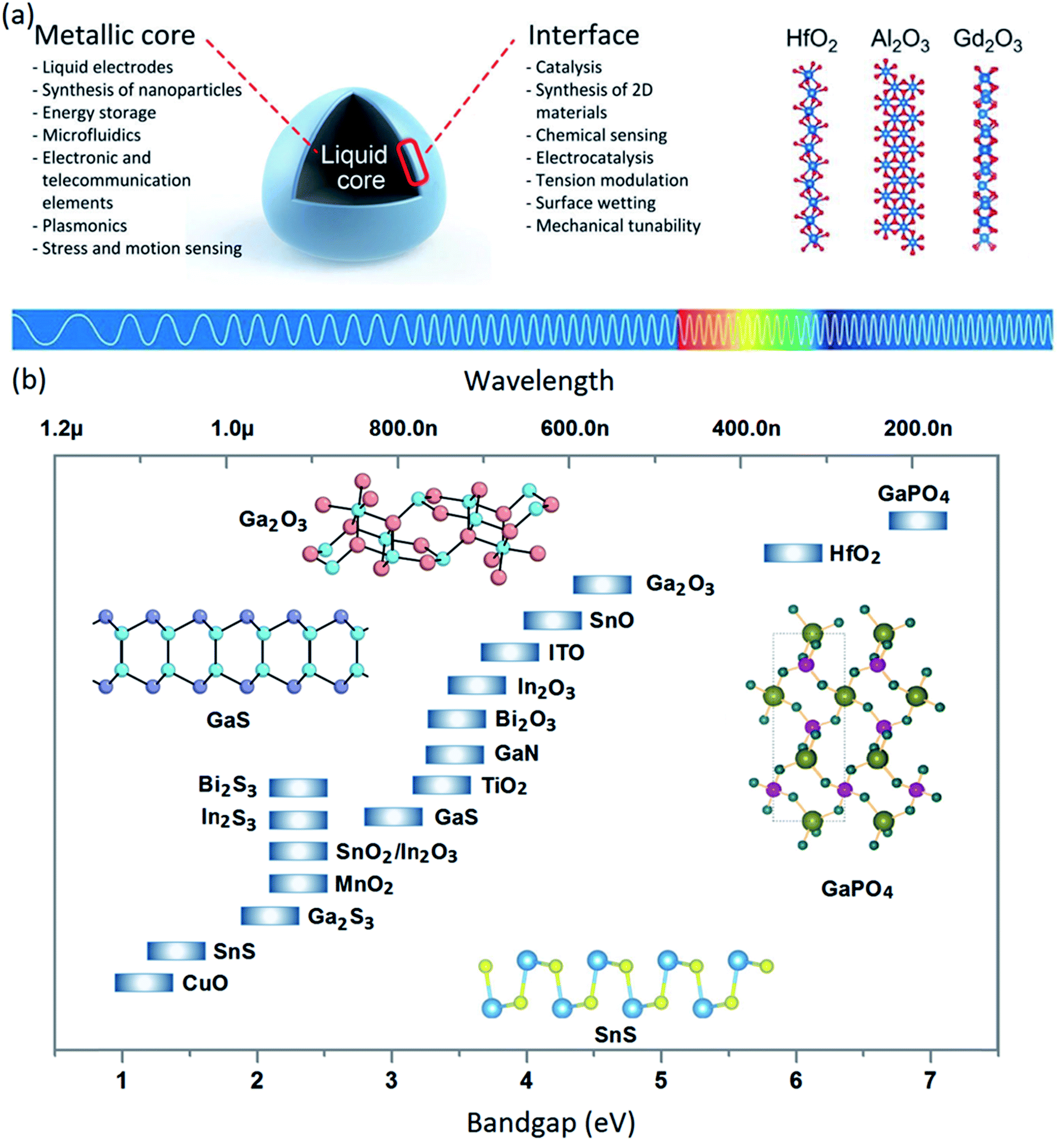 | ||
| Fig. 1 (a) The schematic representation of a liquid metal droplet, which shows the ultra-thin surface oxide films adjacent to the atmosphere. Several applications of the metallic core and metal oxide interfaces are mentioned. (b) The electronic bandgap of synthesized 2D surface oxide films from liquid metals and alloys. (a) is reproduced with permission from ref. 38 and 82. | ||
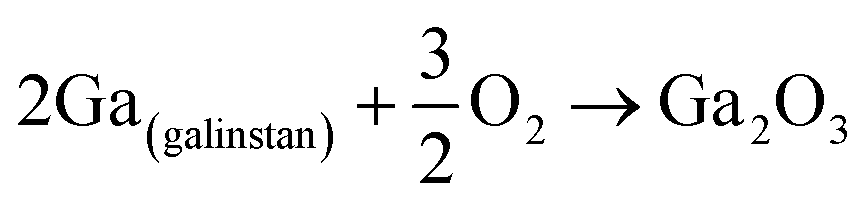
The chemical compositions of 2D surface films of liquid metals are determined by the nature of the surrounding gas. In the ambient atmosphere, the surface films are composed of oxide films of liquid metal. In the alloy liquid metals, the surface oxide film is composed of the thermodynamically stable oxide film of one component of the alloy. For example, the 2D surface oxide films of gallium and tin liquid metals in the ambient atmosphere are Ga2O3 and SnO2, while the thermodynamically stable surface oxide of the galinstan alloy (Ga, In, Sn) is Ga2O3.43–50 The outstanding properties of this type of 2D material have recently attracted the attention of researchers. However, the research activities dedicated to synthesis, characterization and evaluation of the properties of nanomaterials based on 2D surface oxide films of liquid metals are still in their infancy. The elemental composition, atomic structure, temperature-dependent fluidity and thermodynamic characteristics at the liquid metal/surrounding interface and several unknown parameters are engaged in the formation, nucleation and growth mechanisms of surface skin films of liquid alloys, which finally determine the chemical composition, physico-chemical properties, uniformity and thickness of the electronic states of extracted 2D films.51
The present paper reviews the fundamental concepts and the most recent findings in the emerging field of 2D surface skin semiconductors of liquid metals. While there are several research articles which have introduced the concept of 2D surface oxide films of liquid alloys, there is no published review that specifically focuses on the different 2D surface oxides of liquid alloys and holistically summarizes the latest findings in this field. Moreover, considering the importance of metallurgical and thermodynamic parameters on the growth and structural properties of 2D films, these factors are additionally discussed and addressed. Regarding the uniqueness of synthesized 2D surface skin films, attention is individually given to the synthesis, characterization and properties of these 2D nanostructures. The electronic devices based on developed 2D surface oxide films of liquid metals are also introduced and their unique properties and future applications are discussed. Furthermore, the post-processing of natural surface oxide films of liquid metals has recently led to the development of novel types of transition 2D materials which is additionally discussed in the present review. Finally, the focus is also on wafer-scale patterning of 2D surface oxide and post-transition films of liquid alloys, which recently opened up brand-new opportunities for the large-scale synthesis of 2D surface skins of liquid metals and their post-transition semiconductors.
2. The fundamental properties of liquid metals and their interfaces
2.1 Monophasic versus biphasic liquid metals
Liquid metals and their alloys are recognized by their concentration range and phase structures.52–54 The monophasic alloys are liquid alloys where the alloying elements are homogeneously distributed in the alloy and phasic segregations are not observed throughout the liquid. Post transition metals (Ga, In, Sn, Pb, Al and Bi) and group 12 elements (Hg, Zn, and Cd) are the main components of low melting monophasic liquid alloys, which could be combined together to produce monophasic alloying liquid metals with lower casting temperatures.On the contrary, the biphasic liquid metals contain a combined mixture of liquid and solid phases. A biphasic alloy can be produced either by deviation from the alloy eutectic composition or via introduction of solute elements into a monophasic alloy above their solubility limitations in the main liquid metal.55,56 The stability of insoluble components in biphasic liquid alloys is related to the particle size and distribution of the colloidal suspension of solid nano- and micro-particles inside the liquid alloys. The biphasic nature of liquid metals facilitates the incongruent melting of these eutectic alloys. As the melting process in eutectic biphasic alloys is gradual, the composition of the alloy can be variable as a function of cooling temperature.56,57 The low directional dependency is the main characteristic of metallic bonds in metal alloys in both solid and liquid states. The low directional dependency of metal bonds is also responsible for the high boiling temperature of liquid metals. However, the melting temperature of solid materials is dependent on their crystalline structure and the binding energies of the solid structure. The ionization degree of the metal atoms' valence electron in the alloy is an additional factor determining its melting temperature.58–60 Thus, the various crystalline structures and different levels of incorporation of alloying elements impact the liquid metal melting temperature. One of the most famous low-melting post-transition metals is gallium (Ga), which contains both covalent and metallic bonding in its solid state. The closest distance between one gallium atom and its neighbour is 2.7–2.9 Å, indicating a significant distance between two gallium dimers.60,61 This large distance between dimers is responsible for the appearance of strong anisotropy between gallium atoms specifying the weak atomic bonding between adjacent Ga atoms. In fact, this weak atomic bonding is responsible for easy break up of Ga crystals at room temperature.62–64 Similarly to eutectic alloys, the incorporation of additional metallic elements into Ga alloys is accompanied by a further decrease of the Ga melting temperature. A famous reported example of alloying effects on the Ga melting temperature is the Ga–In alloy with a melting point of 16 °C at the eutectic point (Ga–14.2 wt% In).38,65 Ga–In is not the only alloy with such a low melting temperature. There are several other alloys where the incorporation of alloying elements was also accompanied by a further decrease of the melting temperature. In this regard, galinstan, or the ternary Ga, In and Sn alloy, is one of the most famous non-toxic low-melting alloys. While the galinstan melting point has been reported to be as low as −19.1 °C, this temperature refers to the melting point due to the super cooling of the liquid galinstan alloy. However, the real galinstan melting point can be variable from 7 to 25 °C. The decreased melting point of the galinstan alloy originates from the altered average inter-atomic distance by incorporation of In and Sn atoms into the Ga alloy.38,66,67 Other important reasons for galinstan's low melting temperature arise from the role of In in galinstan structures. The surrounding localized charge density (free-electron) around the In atoms in the Ga–In–Sn alloy is tangibly lower than the charge density around the two other components of galinstan. Consequently, In atoms are not attached to each other and can freely move. In this case, the In atoms work similar to a lubricant between the other galinstan alloying elements. The schematic model for atomic distribution inside the eutectic GaInSn alloy was obtained via density functional theory (DFT) calculations and is depicted in Fig. 2a.38
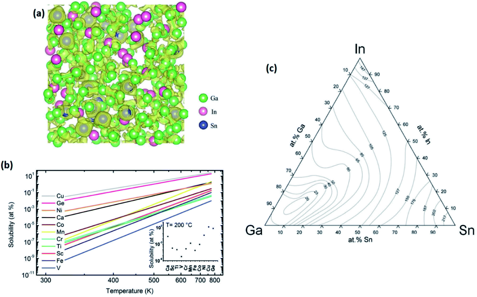 | ||
| Fig. 2 (a) The DFT calculation shows the atomic distribution in the eutectic GaInSn alloy. (b) The temperature dependent solubility of selected metallic elements in liquid Ga. (c) The ternary phase diagram of the GaInSn alloy. Reproduced with permission from ref. 38. | ||
The formation of eutectic alloys can also considerably alter the melting temperature of the binary and ternary alloys. Table 1 shows some famous metal elements and alloys with low melting temperatures. From the metallurgical point of view, a high level of alloy solubility is gained when the difference between the host element atomic diameter and that of the alloying element is less than 15%, the crystalline structure of the host and alloying element is similar and the electronegativity of the alloy elements is close to each other.38,69 For example, Fe cannot fulfil the requirement of high solubility in Ga. Therefore, the formation of a low temperature eutectic alloy in the Ga–Fe system is not possible.68,69 This specific requirement confirms that most of the periodic table elements are considered non-soluble or low-soluble for Ga. Fig. 2b depicts the temperature dependent solubility of the selected elements in liquid Ga. It was practically demonstrated that the molar concentration of alloying elements in liquid Ga is in the range of a few mmol L−1. The graph in Fig. 2c also shows the effects of alloying concentration on the liquidus curve of the ternary eutectic Ga–In–Sn alloy.38 The effect of temperature on solubility of alloying elements in the liquid metal is an additional important factor for the composition of binary and ternary alloys. For instance, the solubility of alloying elements in galinstan can vary by several orders of magnitude by increasing the temperature of liquid alloy.69 As a practical example, the solubility of cobalt in liquid Sn is 3 orders of magnitude higher than the solubility of Ga in cobalt at the same testing temperature. Therefore, understanding the metallurgical and thermodynamic aspects of low temperature liquid metals and their alloys is critically important for comprehension of the thermodynamics of the 2D surface skin liquid metals. Unfortunately, our current knowledge about the thermodynamic and metallurgical aspects of multi-component liquid alloys is quite limited and an understanding of the factors affecting the host alloy and solvent element behaviour is required. Hence modern research is progressing toward the understanding of metallurgical aspects of element solubility in liquid metals and alloys.
| Alloyed elements | A (at%) | B (at%) | C (at%) | D (at%) | E (at%) | Melting point (°C) |
|---|---|---|---|---|---|---|
| Ga/In (EGaIn) | 85.8 | 14.2 | 0 | 0 | 0 | 15.4 |
| Ga/In/Sn (galinstan) | 78.3 | 14.9 | 6.8 | 0 | 0 | 13.2 |
| In/Sn/Bi (Field's alloy) | 60.1 | 18.8 | 21.1 | 0 | 0 | 62.0 |
| Bi/Pb/Sn (Newton's alloy) | 40.7 | 16.4 | 42.9 | 0 | 0 | 98.0 |
| Bi/Pb/Sn (Rose's alloy) | 43.1 | 23.5 | 33.4 | 0 | 0 | 95.0 |
| Bi/Pb/Sn (D'Arcet's alloy) | 43.0 | 24.3 | 32.7 | 0 | 0 | 95.0 |
| Bi/Pb/Sn (Onion's alloy) | 43.3 | 26.2 | 30.5 | 0 | 0 | 92.0 |
| Bi/Pb/Sn/Cd (Wood's alloy) | 41.5 | 20.9 | 18.3 | 19.3 | 0 | 70.0 |
| Bi/Pb/Sn/Cd (Lipowitz's alloy) | 42.1 | 22.9 | 19.3 | 15.7 | 0 | 74.0 |
| Bi/Pb/Sn/Cd/In (French's alloy) | 31.5 | 17.1 | 14.4 | 11.7 | 25.3 | 46.9 |
2.2 Liquid metal interfaces: formation and characteristics
The outer layer of liquid metal is highly active and ready to react instantly with atmospheric oxygen even at very low oxygen pressure forming in a self-limiting metal oxidation reaction.47 Upon exposure of most of the outer layer of liquid metal to the atmosphere, the atomically thick oxide film emerges representing an almost perfect and naturally developed planar 2D material. The ultra-thin oxide films on the Ga surface as well as indium, tin and bismuth alloys are formed even at a very small oxygen partial pressure in the reaction environment.47,70,71 The formation of ultra-thin surface oxide films suppresses further oxidation of the inner layers of liquid metals. The initial oxidation process on the surface of liquid metals can only be suppressed under ultra-high vacuum conditions. The growth mechanism of surface oxide films is based on the ionic transfer between the liquid metal core and the atmospheric environment via the surface oxide film. The establishment of electric potential across the oxide film controls the self-limiting growth of skin oxide films.38,72,73 The surface absorbance of electrons on the metal oxide surface can contribute to the energy state of the surface oxide film with more positive energy than the filled balance band of metal oxide and more negative energy than the work function of the base metal alloy. When the oxygen atom is adsorbed on the liquid metal surface, the electron transfer through the oxide film helps to reduce the oxygen atoms. This process is accompanied by the development of electrostatic potential between the metal/metal oxide and metal oxide/air interfaces.74 The created electrostatic potential, which is called the Mott potential (range of a few eV), controls the growth of the skin oxide film. The magnitude of the Mott potential determines the growth of the surface oxide film.75 When the surface oxide film is ultra-thin, the ions can be easily driven through the surface oxide film via a strong electric field to form the oxide film. Once the surface oxide film becomes thicker, the electric field cannot efficiently drive the ionic species through the thick surface oxide film, thus the further oxidation of metal atoms is hindered. By this mechanism the metallic core is protected from further oxidation.74,75 The liquid metal work function, temperature of the oxidation environment and solubility of the metal and oxygen ions in the oxide film combined are vital parameters determining the oxidation and therefore controlling the final thickness of the natural protective layer. For example, for Ga2O3 film growth on the Ga surface with an estimated thickness of 0.3 to 0.5 nm, the experimental results confirmed that a low pressure of 180 × 10−6 Torr for a time span of 1 s is enough to complete such growth.76 Interestingly, an increase of the temperature up to 300 °C or the same oxygen level does not considerably affect the thickness of the surface oxide film on the Ga liquid metal.77 It was also observed that this 2D surface gallium oxide film mostly consists of amorphous Ga2O3.76,77 It is noteworthy that the 2D surface oxide films of other liquid metals have different growth characteristics which require individual investigation.In the case of liquid metal alloys with different alloying elements the 2D surface oxide film is mostly composed of the thermodynamically stable metal oxide film of a particular component of the liquid metal alloy. This oxidation process is accompanied by the highest Gibb's free energy reduction in the system (ΔGf).78 Take the eutectic In–Sn alloy as an example, where the surface oxide film is mostly made up of a indium oxide film with 6 wt% tin oxide. The surface oxide of liquid metal alloys provides a valuable and unique opportunity to synthesize 2D alloying films similar to the transparent indium tin oxide (ITO) film for electronic applications.79 Another example is the natural surface oxide of the galinstan (Ga–In–Sn) alloy which is mostly constituted of Ga2O3.80 This is because of the lower ΔGf of Ga2O3 than of In2O3 and SnO2 in the oxygen atmosphere. As already mentioned above, the properties of surface films are totally dependent on the interactions at hetero-interfaces between liquid metals and their surrounding environment. Therefore, the exposure of the liquid metal to various environments facilitates the growth of different types of 2D surface compounds. Some of these surface compounds are not naturally available in the layered forms or 2D structure, and thus it is impossible to synthesize them using existing exfoliation techniques. As an ideal example, when the galinstan surface is exposed to HCl, the native gallium oxide instantly reacts with hydrochloric acid, which leads to immediate removal of gallium oxide (reaction (1)). The following interaction of the fresh Ga surface with hydrochloric acid leads to the buildout of metal chlorides and H2O (reaction (2)).81
 | (1) |
| Ga2O3 + 6HCl → 2GaCl3 + 3H2O | (2) |
In the case of the galinstan alloy, since the InCl4 ΔGf is higher than that of SnCl2 and GaCl3,81 the surface of the galinstan alloy in a HCl atmosphere is mostly composed of InCl3 (reaction (3)).81
| GaCl3 + In → InCl3 + Ga | (3) |
These observations confirmed that the formation and growth mechanisms of the surface skin layer on the liquid metal films are governed by thermodynamic rules. Thus, the control of metallurgical and thermodynamic parameters enables researchers to create novel 2D semiconductor nanostructures with desired characteristics. The following sections will be specifically focused on the recently developed and synthesized 2D films originating from liquid metal platforms. To be specific, critical thinking about applications and the outstanding electronic properties of the synthesized ultra-thin 2D films is discussed.
3. Synthesis and characterisation
The characteristics of the liquid metal outer layer with its surrounding environment facilitate a unique platform for growth of unusual 2D materials with attractive functional applications. The high-quality, stress- and defect-free interface between liquid metal and its surrounding environment is one of the highest quality substrates for 2D film growth. Low-melting-point post transition metals such as Ga, In and Sn undergo self-limiting Cabrera–Mott oxidation in air, leading to the development of 2D nanometre-thin surface oxides. Due to the non-polar nature of liquid metals, the attraction forces between the liquid metal substrate and the emerging 2D oxide films are weak and localized. Hence the isolation of surface oxide films from their host alloy is fairly possible. It should be stressed that this liquid metal property enabled the mechanical separation and exfoliation of the liquid alloy surface oxide films form their host alloy.38 Different separation techniques can be employed to separate 2D surface oxide films from their liquid metal substrate. They include sonication in a liquid medium, touching of liquid metal with an appropriate selected substrate and separation of the substrate from the liquid metal, mechanical rolling of the liquid metal and alloy over the smooth substrate as well as separation and extraction of 2D films through density differences and gradients between the synthesized compounds.82 Thus, the following sections individually introduce various synthesis methods of 2D liquid metal surface oxide semiconductor films.3.1 The van der Waals (vdW) exfoliation techniques in the solid state
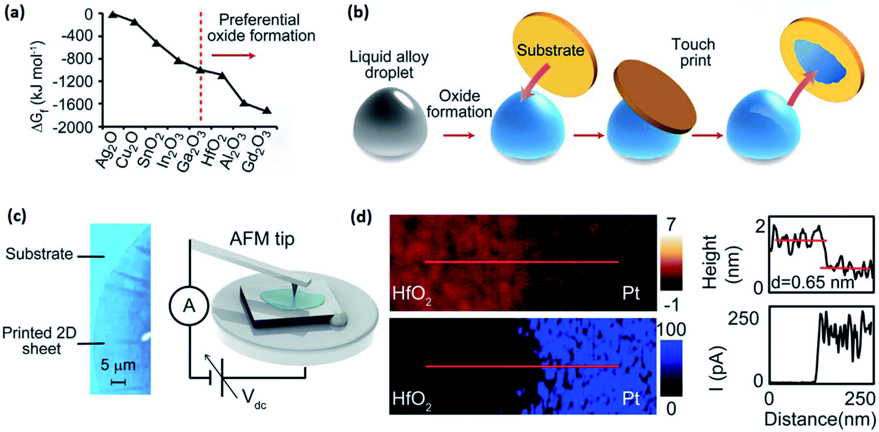 | ||
| Fig. 3 (a) The graph of Gibbs free energy for various metal oxides. (b) Schematic representing the vdW exfoliation technique. The liquid metal alloy droplet is initially exposed to an oxygen-containing atmosphere. Touching the metal droplet with a substrate similar to silicon or glass allows the transfer of the interfacial oxide layer onto the substrate. (c) The optical image of the 2D surface oxide film which was used for AFM studies. (d) The AFM measurement confirmed the ultra-thin thickness (0.65 nm) of the synthesized 2D film. Here the film was HfO2 which is also characterized as a high K material after the measurement of the breakdown electric field. The graphs on the right show, respectively, the profile of the thickness and current corresponding to the maps. Reprinted with permission from ref. 82. | ||
HfO2, as a transition metal oxide, Al2O3, as a post-transition metal oxide, and Gd2O3, as a rare metal oxide, have non-stratified crystalline structures. Consequently, the employment of van der Waals exfoliation technique for these 2D nanostructures is not possible.82,85,86 The exfoliation approaches were proposed to extract 2D nano-films of these typical oxides. The method is based on the exfoliation of the surface oxide film of the galinstan alloy (containing Hf, Al and Gd metals) via touching the liquid metal surface to a suitable substrate that allows transfer of the interfacial oxide layer (Fig. 3b).82 Owing to the liquid metal nature and the absence of microscopic forces between the liquid metal and its natural surface oxide, the vdW exfoliation of 2D films is facilitated and executed.82 It was found that the incorporation of alloying elements into the gallium alloy directly affected the crystallinity of mechanically exfoliated 2D oxide films. This technique has enabled researchers to synthesize high quality flawless 2D crystalline films of HfO2, Al2O3 and Gd2O3 with large-scale lateral dimensions and atomically thin thickness for various electronic applications.82Fig. 3c shows an ultra-thin surface oxide film of the liquid alloy with considerable lateral dimensions. In a case study, the AFM thickness profile and current measurements also confirmed the ultra-thin and insulating nature of vdW exfoliated HFO2 films (Fig. 3d) extracted from the galinstan–Hf liquid alloy. Surprisingly, it was established that while 2D Ga2O3 was amorphous, the HfO2, Gd2O3 and Al2O3 had polycrystalline structures.82,87–89
vdW exfoliation is one of the most employed techniques for preparation of 2D oxide films separated from the surface of liquid metal alloys. The surface oxide film of liquid tin can be an appropriate option to be used for extraction of 2D SnO films. Recently ultra-thin SnO films have been produced via the vdW exfoliation of a tin oxide film from the melted tin alloy at 300 °C.92 Due to the liquid nature of the parent metal, only localised forces occur between the metal and the surface oxide layer, facilitating the cleavage of the oxide layer from the parent metal when the substrate is lifted off. On the other side, the van der Waals interactions along the substrate surface and the oxide layer are not localised and occur across large areas.
The existence of a strong force between the Si/SiO2 substrate and the thin oxide layer on the surface of the liquid metal enables the attachment of the oxide layer to the substrate and facilitates oxide–liquid metal cleavage upon substrate lift-off. After removal of the thick oxide layer, the surface of the liquid alloy was subjected to atmospheric conditions or a continuous purge of oxygen gas inside a glovebox.92 For mechanical delamination of the 2D tin oxide film, the surface oxide film on the surface of the liquid tin alloy was mechanically attached to the Si/SiO2 substrate (Fig. 4a). Due to the vdW force between the substrate and surface oxide film, the tin oxide film is exfoliated from molten tin. The thickness of ultra-thin films in the ambient atmosphere measured using an atomic force microscope (AFM) was approximately 0.6 nm.92 Considering the interlayer spacing of crystalline SnO (0.484 nm), a 0.6 nm thick film can be considered a monolayer SnO film and a 1.1 nm thick film is therefore a bilayer SnO 2D film (Fig. 4b). It was found that the samples synthesized in a glovebox with an oxygen concentration of 10–100 ppm have an ultra-fine and smooth surface, while the surface of 2D films synthesized in the ambient atmosphere is more rough.92 The high-resolution transmission electron microscopy (HRTEM, Fig. 4c and d) studies of synthesized tin oxide films revealed that the nanosheets formed under the ambient atmosphere were composed of two distinct materials with interlayer spacings of 2.7 Å and 3.35 Å, respectively.92 The 2.7 Å lattice spacing is attributed to the (110) plane of SnO, while the 3.35 Å lattice spacing was attributed to the crystalline characteristics of the (110) plane of SnO2. The studies on the electronic properties of the SnO film using the electron energy loss spectroscopy (EELS) technique in the low loss region confirmed that the monolayer SnO film has a direct bandgap nature with a magnitude of 4.25 eV (Fig. 4e).92
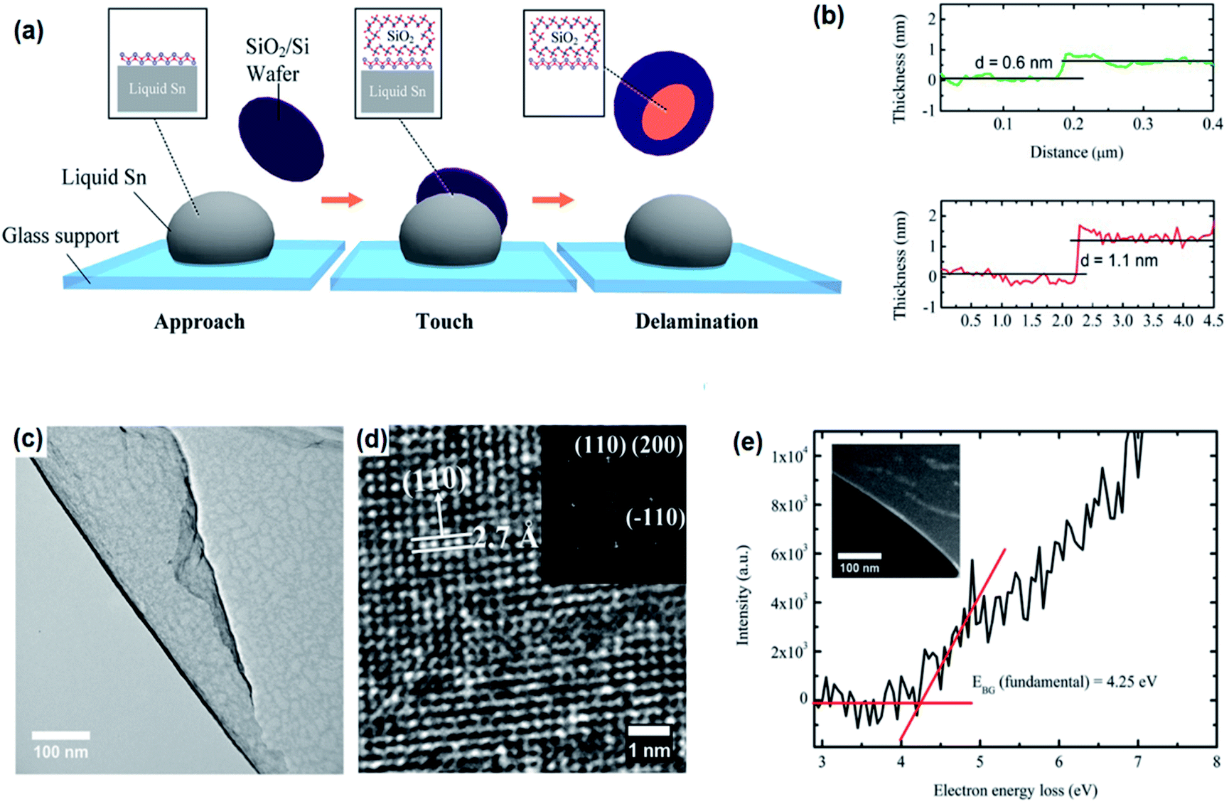 | ||
| Fig. 4 (a) The graphical representation of the vdW exfoliation method. The surface of the molten Sn alloy over the glass substrate is covered with an ultra-thin SnO film. The delamination of the tin oxide film via vdW exfoliation after touching the surface of liquid tin with the Si/SiO2 substrate. (b) The AFM thickness measurement of the monolayer and bilayer SnO film. (c) The HRTEM image of the tin oxide film developed in a controlled atmosphere. (d) The HRTEM image of the SnO film developed in a controlled atmosphere. (e) The bandgap of the monolayer SnO film measured by electron energy loss spectroscopy. Reproduced with permission from ref. 93. | ||
Another research study has also reported the exfoliation of 2D p-type or n-type SnO and SnO2 stoichiometry semiconductors established on the surface of tin liquid metals.105 In the reported results, the effect of oxidation time on the characteristics and properties of 2D tin oxide films was investigated. The characterization studies performed via HRTEM showed the development of multiple tin oxide species (SnO, SnO2, Sn2O3 and Sn3O4) during oxidation of molten tin.106 The studies have also shown that the exfoliated tin oxide nanosheets have a monocrystalline structure with a typically 0.7 nm thickness, corresponding to previously reported values for SnO monolayers.106 A longer oxidation time of molten tin is accompanied by an increase of the oxygen content in tin oxide films and the development of SnO2, Sn2O3 and Sn3O4 components in the form of island oxide nanostructures rather than SnO.106 In the process, larger self-limiting SnO sheets are continuously established on the molten metal which results in the presence of SnO planes under the island oxide structures. The process continues to produce thicker layers in time.106
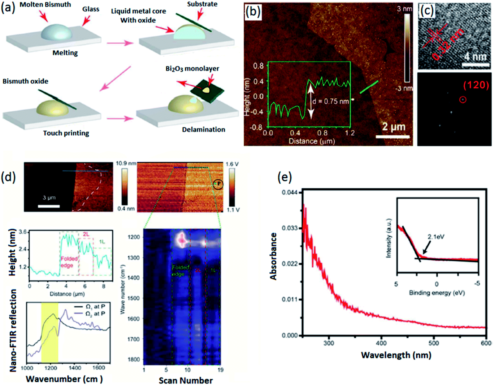 | ||
| Fig. 5 (a) The schematic representation of vdW delamination of the Bi2O3 film in a controlled atmosphere. (b) The AFM thickness measurements and (c) HRTEM image of monolayer α-Bi2O3. (d) The absorbance spectra and (e) the VBM of monolayer α-Bi2O3. Reproduced with permission from ref. 107. | ||
 | ||
| Fig. 6 (a) The schematic representation of the development of vdW heterostructured SnO/In2O3. (b) The HRTEM image of heterostructured SnO/In2O3 films. (c) The highly crystalline structure of the SnO and In2O3 film with the lattice spacing depicted in the HRTEM image of the atomic structure of the heterostructured film. (d) The AFM image of the heterostructured SnO/In2O3 film with (e) the corresponding thickness profile of the film. (f) The Raman spectra of SnO, In2O3 and SnO/In2O3 2D films. (g) The optical absorption of SnO, In2O3 and SnO/In2O3 2D films. (h) The band alignment of SnO/In2O3 2D heterostructures. Reprinted with permission from ref. 116. | ||
The absorption spectra of individual and heterostructured 2D materials have also given valuable information about the optical characteristics of 2D heterostructured SnO/In2O3 films. The maximum optical absorption peak of the SnO/In2O3 heterostructured film is located at 251 nm, which is between 246 nm (SnO absorption peak) and 256 nm (In2O3 absorption peak in Fig. 6g).116–118 It was found that the strong interlayer coupling of the charge carriers affected the optical absorption of the 2D heterostructured film. The bandgap of the 2D SnO film was found to be 4.8 eV, and the value of 3.65 eV was also measured as the bandgap of the In2O3 2D film.116–118 Interestingly, the bandgap of 2D SnO2/In2O3 was narrowed to 2.30 eV.115 The schematic of the band alignment at 2D SnO2/In2O3 heterointerfaces shows that the effective bandgap at the p–n junction is 2.30 eV, which was close enough to the calculated value of the bandgap from the Tauc plot116 (Fig. 6h).
3.2 The squeeze printing technique
 | ||
| Fig. 7 The schematic representation of the screen printing technique of Ga2O3 and GaS. Reprinted with permission from ref. 119. | ||
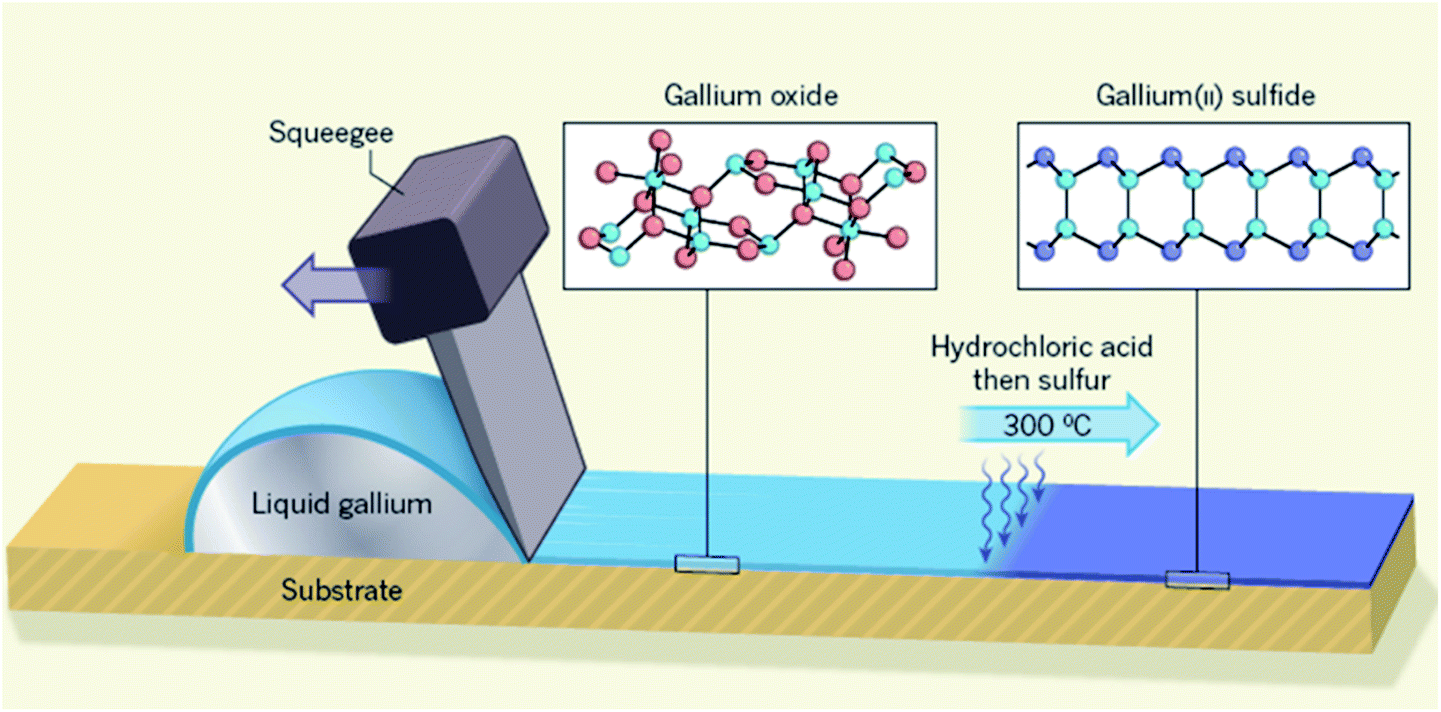
To facilitate substrate surface patterning, the selective area deposition technique was developed where the photolithography technique is accompanied by the surface functionalization of the substrate by perfluorinated silanes.119 The functionalization agent (silane) in the screen printing technique effectively decreases the vdW force between the natural surface oxide of Ga and the substrate preventing the exfoliation and delamination of the surface oxide film. Screen-printing was employed to pattern Ga2O3 on the Si/SiO2 wafer substrate with precise control over the thickness of the rolled liquid alloy. Owing to the instantaneous and rapid oxidation of rolled liquid gallium upon its exposure to atmospheric conditions, Ga2O3 films were continuously deposited over the substrate using the screen-printing technique (Fig. 7).
The post treatment of the 2D materials developed using the screen printing technique is found to be an additional functional approach for synthesis of processed novel 2D materials. An indirect sulphurization technique was employed on Ga2O3 after screen printing of a gallium alloy which finally resulted in the synthesis of 2D gallium selenide films.119 The method includes the passing of hydrochloric acid vapour over the surface of the Ga2O3 film patterned on the Si/SiO2 substrate at 45 °C via a simple rolling/squeezing process. During the sulphurization process the 2D Ga2O3 films were transformed into GaCl3. The following heat treatment at 300 °C was accompanied by the direct transformation of the GaCl3 2D films into a gallium(II) sulphide (GaS) film. This low temperature chalcogenisation step at 300 °C is highly important from a technical point of view since it facilitated the low-temperature fabrication technique of 2D chalcogenide films. On the contrary, the regular chalcogenisation process requires a high processing temperature (900 °C).120–122 The low temperature fabrication techniques are therefore highly desired for semiconductor processing instruments, especially low temperature processing, as the basic technical requirement for fabrication of transparent and flexible electronic devices.
In another study, the screen-printing method was successfully employed to develop a wafer-scale size of the GaS film over the Si/SiO2 substrate with a patterned tungsten electrode.123 In this method, the tungsten was initially deposited on the Si/SiO2 film and the electrodes were prepared by photolithography. Then, the surface of the wafer was immersed in FDTES to functionalize the surface of the Si/SiO2 electrode with a monolayer of fluorocarbon. After the removal of photoresist materials, the patterned substrate was employed for gallium alloy printing. With the screen-patterning method, Ga was rolled on the surface of the Si/SiO2 substrate to produce ultra-thin 2D patterned films. Before rolling, Ga was placed in HCl at 60 °C to remove the natural oxide from the surface. The surface of the printing paper was placed in direct contact with HCl vapour to halogenize Ga2O3 and produce GaCl3. Then the GaCl3 again was placed in direct contact with the sulphur gas to turn it into GaS films. The process is graphically demonstrated in Fig. 8a–d. The two-step sulphurization process helped to reduce the sulphurization temperature of the Ga2O3 film down to 300 °C, since the direct conversion of chemically inert Ga2O3 into GaS requires much higher temperature (900 °C).124–127 Both Raman spectroscopy and XRD characterization confirmed the development of stoichiometric GaS films via this technique. The AFM measurements also certified that the 2D GaS film has the thickness of 1.5 nm, which is equal to the thickness of two fundamental layers of GaS. In addition, TEM observations established that the developed 2D crystalline film has a lattice spacing of 3.1 Å. The bandgap of 2D GaS films was found to be 2.5 eV. Moreover, the photoluminescence studies additionally confirmed that the synthesized 2D films are capable of sensing light in the middle and the end of the visible light spectrum range. Thus, all reported characterization studies endorsed the n-type nature of the synthesized GaS 2D film. The p-type conductivity of the GaS 2D film was gained by exposing the synthesized film to NO2 gas.123 Therefore, a combined screen-printing and two-step annealing approach is considered a strong technique for synthesizing 2D films with a variety of tunable electronic properties.
 | ||
| Fig. 8 The graphical scheme of the wafer-scale development of GaS patterned 2D films on the Si/SiO2 substrate. (a) The lithography process for patterning the Si/SiO2 substrate and production of the lithography mask. (b) The coverage of the exposed area to FDTES vapour. (c) The coverage of the patterned substrate with gallium using PDMS. (d) The two-step process to halogenize and chalcogenize the ultra-thin films on the Si/SiO2 substrate. Reprinted with permission from ref. 123. | ||
A squeeze printing approach was employed to develop an ultra-thin layer of a liquid tin–indium alloy on the substrate.128 The process entails the placing of a small droplet of liquid alloy between two substrates followed by squeezing. This leads to smearing of the liquid droplet on the desired surfaces. The rapid Cabrera–Mott oxidation process of the liquid alloy in the ambient atmosphere was accompanied by the formation a homogeneous surface oxide film during the squeezing of the alloy while the parent liquid metal works as the soft platform for development of the 2D oxide film (Fig. 9a). The AFM thickness profile (Fig. 9b) and the following HRTEM images confirm the large-scale fabrication of the pin-hole free ITO monolayer with micro-scale lateral dimensions over the substrate (Fig. 9c). The HRTEM studies (Fig. 9d) demonstrated that the 2D nanostructures grown from the In/Sn alloy containing an optimized tin concentration (5 at%) featured highly crystalline domains with typical lateral sizes of 20 nm. The decreased sheet resistance is also attributed to the improved crystallinity. The colour enhanced HRTEM studies supported the oriented growth of crystalline domains in the nanostructure of 2D ITO films with an optimized tin concentration (Fig. 9d). The increase of the tin concentration up to 20 at% resulted in the increase of the 2D film amorphicity. Thus, the crystalline domains were surrounded by amorphous phases (HRTEM image in Fig. 9e). It was found that the properties of the developed 2D ITO film are dependent on the percentage of the tin alloying element in the molten alloy. The ratio of tin in the ITO 2D film was found to be higher than that in the parent indium–tin alloy, which is more interesting from the compositional point of view for the 2D ITO film. The characterization of the 2D ITO optical properties revealed that the developed 2D ITO featured minimal absorption across the visible light spectrum leading to only 0.4% transmittance loss for the substrates coated by ITO. The bandgap analysis of 2D ITO corroborated the optical bandgap of 3.9 eV, revealing that the developed 2D ITO is 6.25 times more transparent than the monolayer of graphene.128,137,138 It was also found that the sheet resistivity of the 2D transparent ITO film is a function of the ITO layer number in the film.128 In fact, a continuous reprinting process led to the deposition of a bilayer ITO film with much improved conductivity. Fig. 9f and g depict the monolayer and bilayer 2D ITO films, respectively. It was discovered that the sheet resistance of the ITO bilayer film was 5.4 KΩ sq−1, which is much smaller than the sheet resistance of the developed ITO monolayer (69.6 kΩ sq−1) while 99.3% transparency across the visible spectrum was maintained.127 Thus this study confirmed that repeated printing enabled the subsequent deposition of ITO layers to achieve the desired sheet resistance and transparency of 2D films for their further employment in various electronic applications.
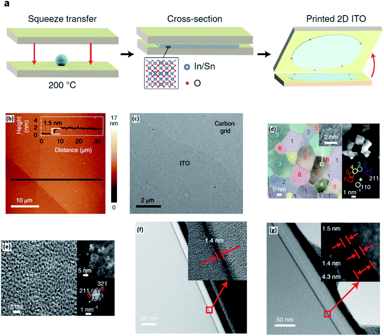 | ||
| Fig. 9 (a) The schematic representation of squeeze printing of the In/Sn alloy for synthesis of 2D ITO. (b) The AFM thickness profile of monolayer ITO. (c) The HRTEM image of the pin-hole free uniform ITO film. (d) HRTEM image of the 2D ITO nanosheet. The colour code highlights the crystal orientation based on the fast Fourier transform (FFT) accompanied by the magnified view of the lattice pattern. (e) The HRTEM image of sheet exfoliated 2D ITO depicting an amorphous structure with occasional crystalline zones. (f) Cross-sectional HRTEM images of monolayer and (g) bilayer ITO films. Reprinted with permission from ref. 128. | ||
3.3 Reactive environment for synthesis of 2D films
3.3.1.1 Ga2O3, and HfO2. An innovative synthesis technique of 2D metal oxide films was developed based on the immediate reaction of gas bubbles with the surface of liquid metals. This approach is based on exfoliation of the surface oxide films via explosion of gas bubbles inside the liquid metal droplet, which is literally called the gas injection method.82 The 2D oxide layer is formed at the hetero-interface between the gas bubbles and the liquid metal during the passing of gas bubbles through the liquid metal. In this technique the liquid metal droplet is sunk in deionized liquid which later allows the uniform dispersion of separated nanosheets on the surface of the deionized liquid (Fig. 10a). The main advantage of this approach over van der Waals (vdW) exfoliation is its considerable scalability. Another important parameter in the gas-injection method is the occurrence of strong reaction between the galinstan alloy and aqueous environment. However, the synthesis of metal oxide nanosheets is still governed by the thermodynamic preference i.e. the oxide with the lowest AGf is the dominant product of synthesis. This was confirmed and demonstrated by synthesis of Al2O3 and Gd2O3 2D nanosheets in an inert solvent.82 The extracted 2D films had considerable lateral dimensions. The obtained materials characterization suggested that the gas injection method in a liquid environment is highly capable of scalable synthesis of non-crystalline pinhole-free 2D oxide films.82 The AFM images in Fig. 10b and c, respectively, depict the microscale-sized 2D Ga2O3 and HfO2 films with atomistic and conformal thickness. It was found that the strong interaction of Al and Gd with the aqueous reaction environment did not allow the further synthesis of 2D Al2O3 and Gd2O3 films. Additional HRTEM, electron diffraction and Raman characterization studies confirmed that the level of crystallinity of 2D Ga2O3 and HfO2 films synthesized by the gas injection method is less than that of the mechanically exfoliated 2D films.82 This is attributed to the shorter reaction time during the synthesis process in the gas injection technique. The reaction time for a regular exfoliation process is considerably longer than that for the gas injection method in a liquid environment. Since the fresh metallic atoms on the surface of the liquid alloy are exposed to the gaseous environment for a considerably longer time prior to vdW exfoliation, the conditions for facile reorganization of crystalline structures are provided.82
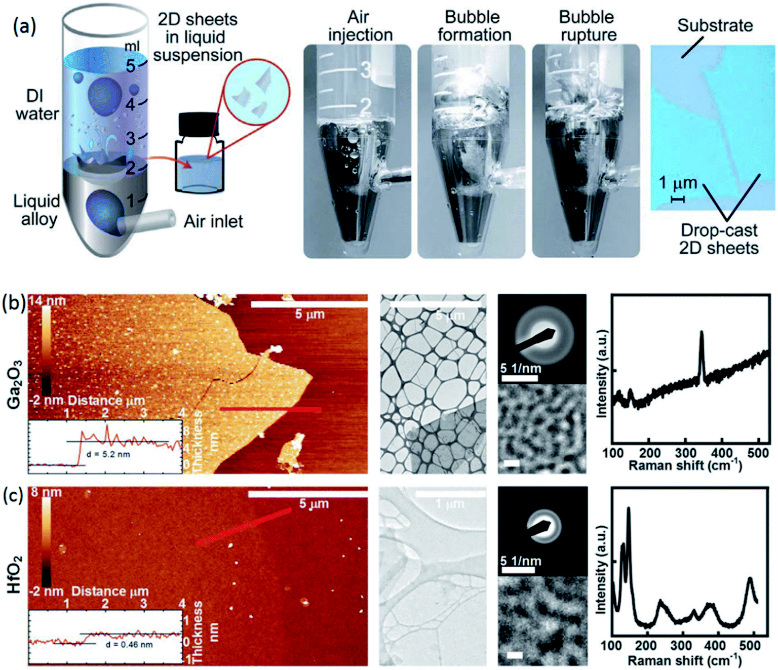 | ||
| Fig. 10 (a) The schematic showing the gas injection method (left) and the bubble bursting inside the liquid metal and thus producing the 2D surface oxide films. The optical image of drop-cast 2D nanosheets. (b) and (c) respectively show the AFM images, the HRTEM studies and the Raman spectra of Ga2O3 and HfO2 films synthesized by the gas injection method in an aqueous environment. Reproduced with permission from ref. 82. | ||
3.3.1.2 Cobalt oxide. In another research study, 2D cobalt oxide nanosheets were synthesized via injection of O2 gas inside a liquid galinstan droplet containing various weight percentages of a cobalt alloy.138 To prevent the formation of gallium oxide nano-flakes, HCl was introduced into an aqueous solution to minimize the formation of natural surface oxide layers and to control the pH of the solution at an acidic level.138 It is well known that acids will dissolve natural gallium oxide on the surface of a galinstan alloy containing elemental Co. The solution containing 10 mM HCl was found to be effective enough to remove the surface oxide film of galinstan.138 The control and minimization of the formation of gallium oxide facilitate the oxidation of metallic Co in the alloy. The explosion of oxygen bubbles inside the galinstan alloy containing Co resulted in the generation of CoO 2D nanostructures.138 A significant number of defects was found in the synthesized nanosheets and was denoted as CoOx. Thermodynamically, the oxidation of gallium in the galinstan–Co alloy is preferred; however the dissolution of gallium oxide in 10 mM HCl subsequently promotes the formation of CoOx in solution via the Cabrera–Mott oxidation process which limits the growth of the oxide layer at the surface of the galinstan–Co alloy to several Å.138 The synthesized CoO films have an atomic-scale thickness in the range of 1 to 4.5 nm with lateral dimensions of 200 nm.138 It was also found that the dissolution of CoO in aqueous solution only begins when the concentration of HCl is equal to or more than 0.5 M.138 Thus, a 10 mM concentration of HCl in an aqueous environment is enough to dissolve any type of Ga2O3 nanostructure, but still allows for CoOx to exist in solution.
3.3.1.3 SnOx nanoflakes. A Sn–Bi alloy was employed in the gas injection method in an aqueous solvent to synthesize SnOx nanoflakes.139 Previously, the scaleable synthesis of 2D gallium oxide, hafnium oxide and cobalt oxide was successfully achieved via continuous injection of oxygen gas into the liquid metal alloys.82 Most of the above mentioned alloys have melting temperatures less than 100 °C. However, synthesis of some nanomaterials similar to SnOx nanostructures via the gas injection method requires the employment of a Sn alloy with a melting temperature of 231.9 °C.139 The Ga–Sn alloy has a low melting temperature and consequently it can be considered a valuable candidate. However, the thermodynamic conditions facilitate the preferential growth of Ga2O3 and thus prevent the availability of the Ga–Sn alloy for synthesis of the 2D SnOx film. Therefore, a mixture of the Sn and Bi alloy was prepared and used in a V-shaped quartz tube, where the oxygen gas was injected inside and then passed through the liquid Sn–Bi alloy. The alloy was covered with diethylene glycol on top which acted as a dispersion solvent. The metal oxide skin was later dispersed in the liquid metal and finally floated on the surface of the dispersion solvent (Fig. 11a).139 These synthesis approaches led to the production of different types of nanostructures with various morphology and crystallinity. 2D freestanding amorphous nanoflakes and nanosheets of SnOx were found in TEM and STEM studies with a uniform thickness of ∼5.0 nm (Fig. 11b–d).139 This process also led to the synthesis of crystalline SnOx nanoflakes and nanorods as the by-products of this technique. The other main by-products of this synthesis were BiOx nanoparticles and single atoms and clusters of bismuth which were found on the amorphous 2D SnOx nanoflakes.139
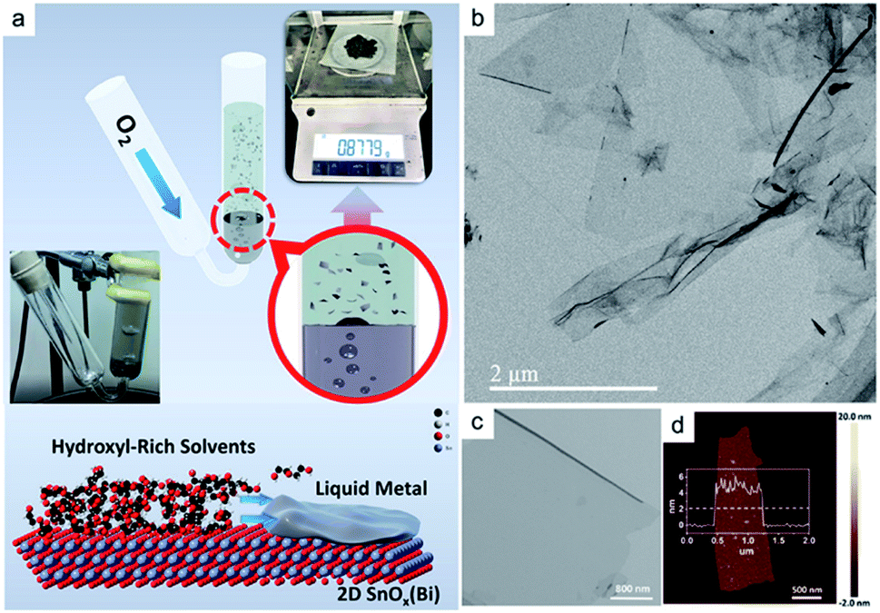 | ||
| Fig. 11 (a) The schematic image shows the principles of synthesis of 2D SnOxvia injection of O2 gas into a Sn–Bi alloy. High hydroxyl solvents remove the remaining galinstan from the surface of 2D SnOx nanoflakes. (b) and (c) show the TEM images of 2D SnOx nanosheets, accompanied by (d) the AFM thickness profile of freestanding nanosheets. Reprinted with permission from ref. 139. | ||
3.3.1.4 Green synthesis of 2D Al2O3 flux membranes. The large-scale green synthesis of γ-AlOOH nanosheets in reactive liquid was introduced recently. This method opened up a new platform for synthesis of functional green materials with environmental applications.140 One of the main precursors employed for synthesis of aluminium oxide is oxide hydroxide of aluminium (boehmite γ-AlOOH).141–144 γ-AlOOH turns into Al2O3 nanosheets via the annealing process. The controlled crystalline structure and the morphology of boehmite are important since they determine the characteristics of processed Al2O3 films after the annealing process.145–148 γ-AlOOH as a highly stable compound at room-temperature with a wide bandgap is an attractive option for various environmental applications.149–152 The layered structure of γ-AlOOH and its high stability have opened up tremendous applications in composite materials, medicine, catalysis, ceramics, electronics, and other technologies.149–152 As a stable compound, γ-AlOOH can be synthesized by several methods which mostly require high temperature, intense power and long processing time. In addition, the existing production techniques are usually accompanied by the release of toxic chemicals.153–159 An alternative green synthesis approach has recently been developed to fabricate 2D γ-AlOOH nanosheets based on instant interactions between the surface of liquid galinstan metal and H2O in the liquid environment (Fig. 12a). The technique includes the rapid interaction of a galinstan alloy containing 3.3 wt% Al with aqueous environment ether in the form of liquid or vapour phases.140 The interaction of the galinstan alloy with distilled water (DIW) occurred along with the rapid formation of gas bubbles on the liquid metal interface facilitating the delamination of 2D surface oxide films of the galinstan alloy from the surface. The final product is hydrogel containing 2D nanosheets of γ-AlOOH. It was observed that when water vapour gas was employed as the reactive environment, the final products represented the combination of 1D fibrous and pillar nanostructures perpendicular to the surface of the liquid galinstan alloy. The growth of fibrous γ-AlOOH nanostructures continues until the ultimate consumption of aluminium in the galinstan alloy (Fig. 12a–c).138 The proposed mechanism for the chemical synthesis and the growth of boehmite γ-AlOOH is mentioned in the equations given below:140
| 2Al + 6H2O → 2Al(OH)3 + 3H2 | (4) |
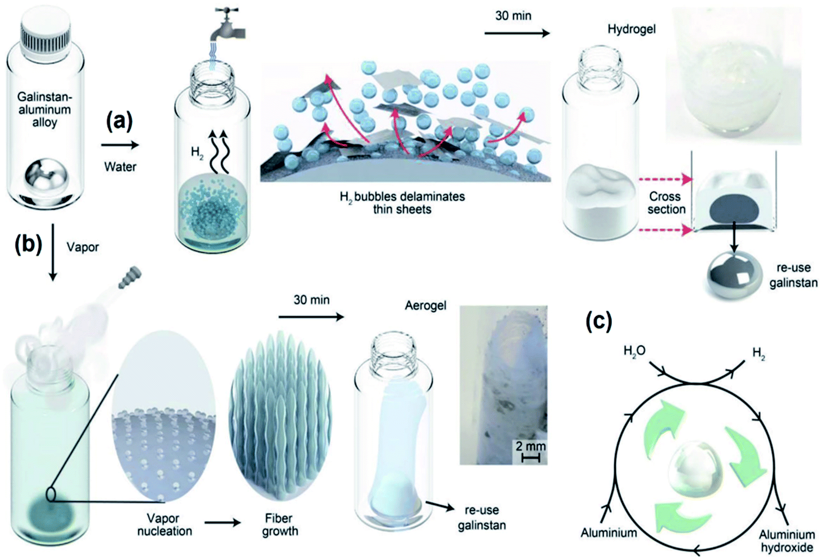 | ||
| Fig. 12 The schematic of the interaction of a galinstan alloy containing Al with (a) DIW and (b) vapour steam which resulted in the formation of either (a) hydrogel or (b) aerogel via (c) the surface interaction of H2O with the surface of galinstan. Reprinted with permission from ref. 140. | ||
The following heating of hydrogel products at 170 °C for 4 hours is accompanied by the transformation of Al(OH)3 into AlOOH (eqn (5)):
| Al(OH)3 → AlOOH + H2O | (5) |
Furthermore, it is also possible to facilitate the single step-growth of AlOOH, where the galinstan alloy surface is subjected to H2O vapor (eqn (6)):
| 2Al + 4H2O → 2AlOOH + 3H2 | (6) |
Finally, the following annealing at 550 °C is required to turn the AlOOH into Al2O3 (eqn (7)):
| 2AlOOH → Al2O3 + H2O | (7) |
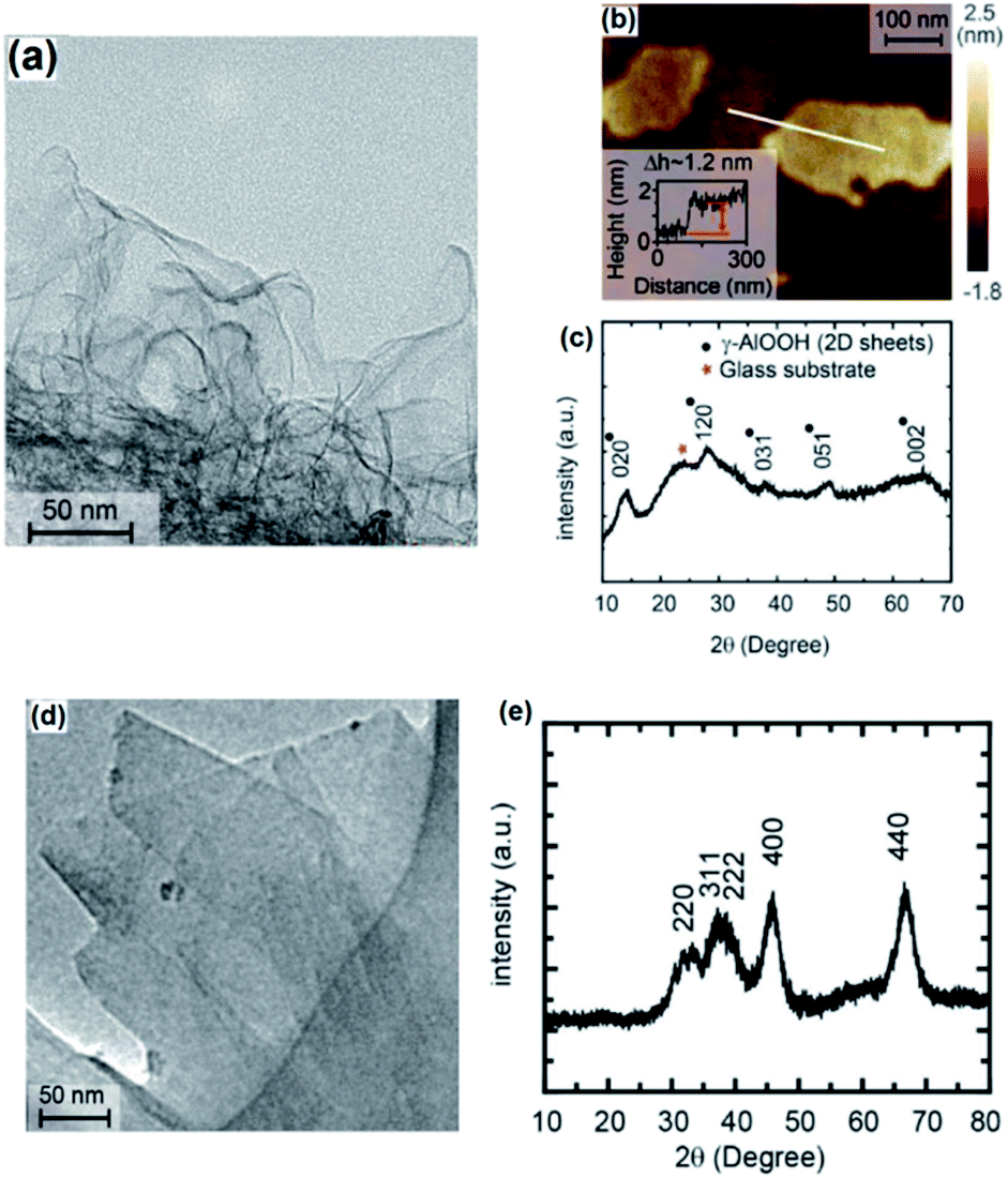
The characterization studies confirmed the crystalline nature of 2D AlOOH nanosheets. The HRTEM studies combined with XRD show (Fig. 13a and c) that γ-AlOOH had an orthorhombic structure with lattice spacing parameters of a = 3.700 Å, b = 12.227 Å and c = 2.868 Å.140 The AFM investigations further confirmed that the AlOOH 2D nanosheets had a 1.2 nm thickness (Fig. 13b and c). After thermal annealing of boehmite nanosheets at 550 °C, the γ-AlOOH ultimately turned into crystalline 2D layered Al2O3 (Fig. 13d and e). This green synthesis approach was found to be a reliable and cheap alternative method for large-scale synthesis of 2D nanostructured metal oxide based on reactive interaction of liquid metals in an aqueous environment. The high efficiency of synthesis of 2D Al2O3 nanosheets with reduced reaction time and processing temperature was supported by the facile synthesis of high quality 2D materials with perfect crystalline structures, high mechanical stiffness and considerable Young's modulus for application in harsh environments.140
 | ||
| Fig. 13 The results of characterization of (a–c) γ-AlOOH and (d and e) γ-Al2O3. Reprinted with permission from ref. 140. | ||
3.3.1.5. MnO2. Recently it was established that the interfacial interactions between a liquid metal and its surrounding liquid environment can successfully enable the synthesis of novel 2D materials.82 Galvanic replacement reactions represent some of the most interesting chemical phenomena happening at interfaces between the liquid metal and its surrounding ionic liquids.160–165 The self-limiting interactions at the liquid metal interfaces demonstrate the successful growth of 2D metal oxides with atomically thin characteristics. A synthesis method based on interaction between a liquid eutectic gallium–indium (EGaIn) alloy and its surrounding liquid solution has successfully produced single-layered hydrated MnO2 nanosheets.163 The method is based on reduction of permanganate ions on the surface of liquid galinstan. The galvanic replacement of ionic species in liquid solution with the EGaIn alloy led to the growth of nanosheets on the surface of EGaIn droplets in the form of shells (Fig. 14a).166 The direct redox reaction between EGaIn and permanganate ions [KMnO4 (Mn7+)] resulted in the formation of hydrated MnO2 on the surface of the EGaIn alloy due to galvanic interactions (Fig. 14a). Both components of EGaIn can be oxidized during contact with the KMnO4 ion solution. However, when the standard reaction potential of 1.697 V vs. SHE for the MnO4−/MnO2 reaction is considered, it can be found that the Ga replacement by KMnO4 ion species in an ionic solution results in the highest driving force (E0[Ga3+/Ga0] = −0.529 V vs. SHE) compared with indium (E0[In3+/In0] = −0.34 V vs. SHE).164 Since the greatest reduction in the Gibb's free energy occurs due to replacement of gallium via ionic species, the surface of EGaIn serves as the sacrificial platform for the synthesis of hydrated MnO2 sheets (Fig. 14b). The proposed redox reaction between metallic Ga and MnO4 is described by the following equations:165,166
| MnO4(aq)− + 2H2O + 3e− → hydrated MnO2(s) + 4OH(aq)− | (8) |
| Ga(l)0 → Ga(aq)3+ + 3e− | (9) |
| MnO4(aq) + 2H2O + Ga(l)0 → hydrated MnO + Ga3+ + 4OH(aq)− | (10) |
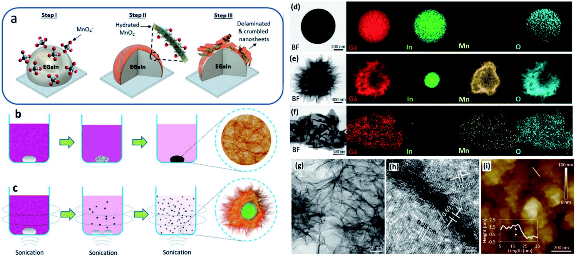 | ||
| Fig. 14 (a) The schematic of the formation of hydrated MnO2 nanosheets on the surface the EGaIn alloy in aqueous solution containing KMnO4. (b) The formation of monolayers of hydrated MnO2 in non-sonication and (c) sonication assisted methods. (d) The EDS analysis shows the distribution of alloying elements on the surface of pure EGaIn particles, (e) alloying element distribution on the surface of hydrated MnO2 nanosheets and (f) the detached shells from the liquid metal platform. (g) The TEM image of extracted MnO2 nanosheets accompanied by (h) the HRTEM image of the crystalline structure of 2D nanosheets. (i) The AFM image of the thickness profile of MnO2 nanosheets. Reproduced with permission from ref. 166. | ||
The direct interaction between the EGaIn alloy and aqueous environment leads to generation of soluble [Ga(OH)4]−.166,167 Owing to the prevailing oxidation process on the surface of the liquid EGaIn alloy, the reactions were found to be self-limiting which is similar to the Cabrera–Mott process. To guarantee the non-stop and continuous access of the fresh EGaIn surface alloy to a Mn7+ ion containing solution, the KMnO4 reactant was introduced into the reaction medium after the establishment of the EGaIn colloidal solution. The produced nanosheets were found to be self-exfoliated, assisting with continuous production of ultra-thin 2D films. The mechanical agitation via the sonochemical assisted synthesis method facilitated the delamination of oxide films (Fig. 14c). This synthesized core/shell nanostructured liquid metal alloy was composed of a porous shell comprising hydrated manganese and gallium oxide sheets surrounded by a solid indium core. The bright field and energy dispersive elemental spectroscopy mapping of sonicated EGaIn droplets demonstrated the uniform deposition of Mn on the surface of EGaIn droplets and synthesized nanosheets (Fig. 14d–f). The TEM studies revealed the crystalline and ultrathin nature of the as-synthesized, delaminated and hydrated MnO2 nanosheets. The HRTEM studies of interlayer spacing (Fig. 14g and h) and AFM studies (Fig. 14i) also confirmed that the MnO2 nanosheet has a monolayer structure.165
3.3.1.6 MoSx. In another research study, EGaIn was used to serve as an ultra-smooth template and reducing agent for the precursor to form large-scale planar molybdenum sulphides transferrable to any substrate.168 The alloying process in Ga based metals is controlled by thermodynamic factors. If the alloying element is present on the surface of liquid metal, it can be oxidized or sulphurized in appropriately selected gaseous environments. However, it requires the dissolution of alloying elements in a gallium based alloy. This fact means that the 2D surface oxide film of an alloying element similar to W and Mo is not soluble in a gallium based alloy and cannot be extracted through the interaction of the gallium based alloy with the surrounding gas environment. The proposed technique is to bring the precursor to the surface of liquid metals containing these metallic elements to enable a desired reaction finally leading to the synthesis of 2D nanostructures or compounds.169 This strategy was employed to develop 2H-molybdenum disulphide (MoS2) 2D films via a series of sequential reactions and washing steps. In this method the surface film of liquid metal galinstan reacted with molybdenum precursors inducing the self-deposition of ultra-thin molybdenum sulphide films on the outer surface of the liquid galinstan droplet. In this process the natural gallium oxide at the surface of liquid galinstan was initially removed by washing the surface of liquid galinstan with a HCl solution (Fig. 15a).168 The fresh surface of galinstan after removal of the Ga2O3 natural oxide film offers excessive electrons on the surface which later can reach the saturation level and then the subsequent equilibrium state. In the equilibrium state no further oxidation occurs at the hetero-interface of the liquid metal and acidic aqueous solution.168 At this stage the surface potential of the galinstan alloy is naturally neutralized by the counter ions inside the aqueous acidic solution. This results in the formation of an electrical double layer (EDL) which is composed of several sublayers (Fig. 15b).168 The interfacial potential was unbalanced by the attached H+ counter ions on the galinstan alloy. Thus, this acts as a driving force to establish the equilibrium potential via interaction of co-ions and counter ions. This helps the outer Helmholtz layer to reach the equilibrium state. The introduction of (NH4)2MoS4 into the reaction environment is accompanied by the substitution of anions in the outer Helmholtz layer via (MoS4)2− (Fig. 15c). The following reaction of H+ in the inner Helmholtz layer resulted in the development of either MoS3 or MoS2 films (Fig. 15d). To further crystallize and sulphurise the extracted 2D films, a three-step annealing process was conducted to facilitate the phase transformation. It was discovered that the generated 2D 2H-MoS2 films after the annealing process have an ultra-thickness of 0.7 nm with a hexagonal atomic layered structure (Fig. 15e and f). The crystalline nature and characteristics of the hexagonal 2H-MoS2 film were later confirmed by HRTEM studies (Fig. 16g and h). An interlayer spacing of 0.6 nm was measured for the 2H-MoS2 film which corresponds well with that of the monolayer MoS2 single crystal.168
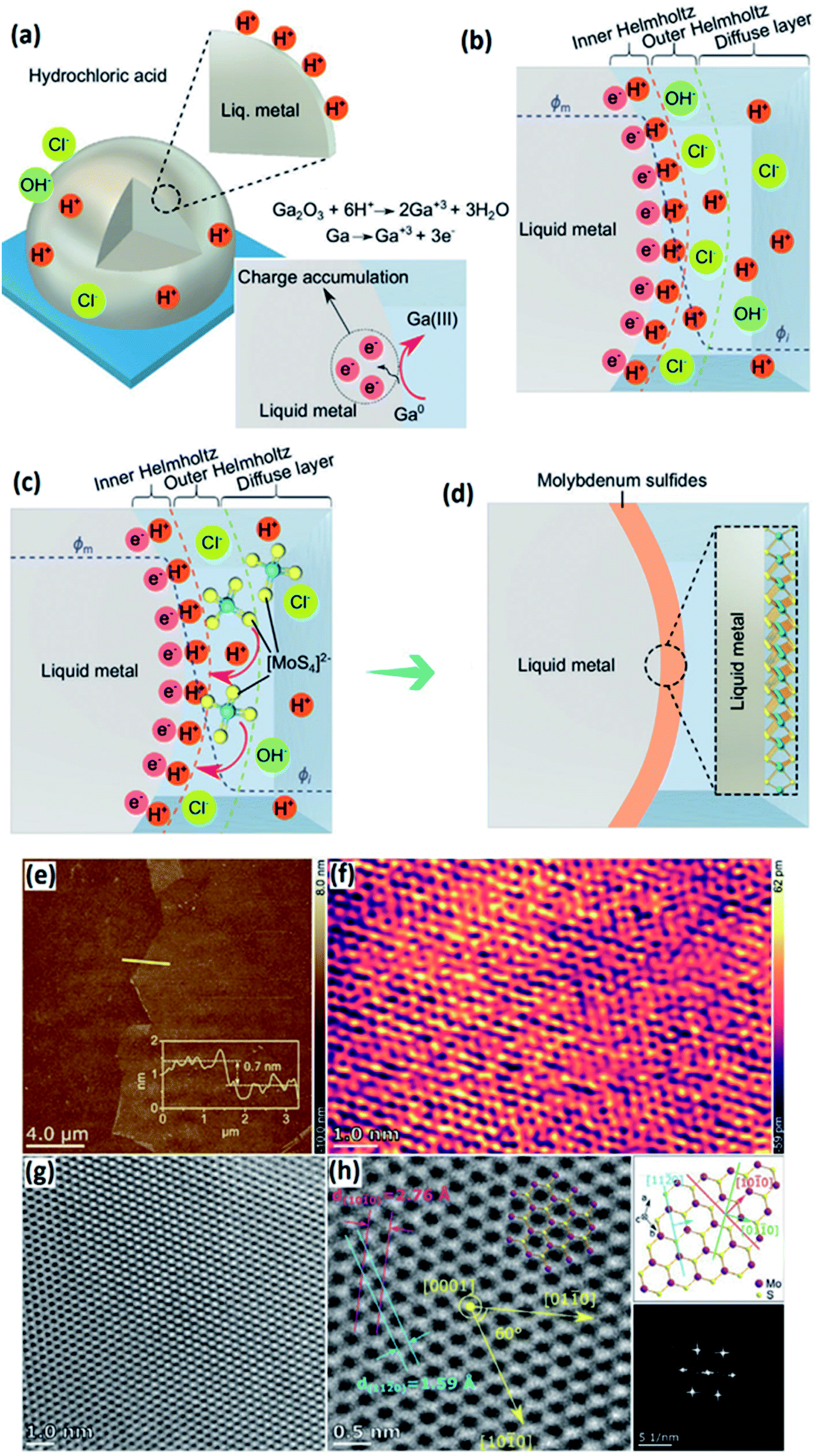 | ||
| Fig. 15 (a) The removal of gallium oxide using an acidic aqueous solution. (b) The saturation and equilibrium of free electrons on the surface of galinstan. The electron confinement on the EDL and formation of the Helmholtz layer. (c) The anodic substitution of ionic (MoS3)2− in the Helmholtz layer accompanied by subsequent reactions with H+ in the inner Helmholtz layer. (d) The formation of the MoSx film on the surface of liquid galinstan. (e) The AFM profile and (f) high-resolution image of the atomic structures of the surface of MoS2 nanosheets. (g) The HRTEM image and (h) crystalline characteristics of 2D MoS2 films. Reprinted with permission from ref. 168. | ||
 | ||
| Fig. 16 The cell configurations used to synthesize 2D-GMs with liquid metal electrodes in (a) anodic aqueous, (b) anodic non-aqueous and (c) cathodic aqueous systems. (d–f) respectively show the HRTEM micrographs of 2D-GNs extracted from synthesis methods of (a) and (b). Reprinted with permission from ref. 169. | ||
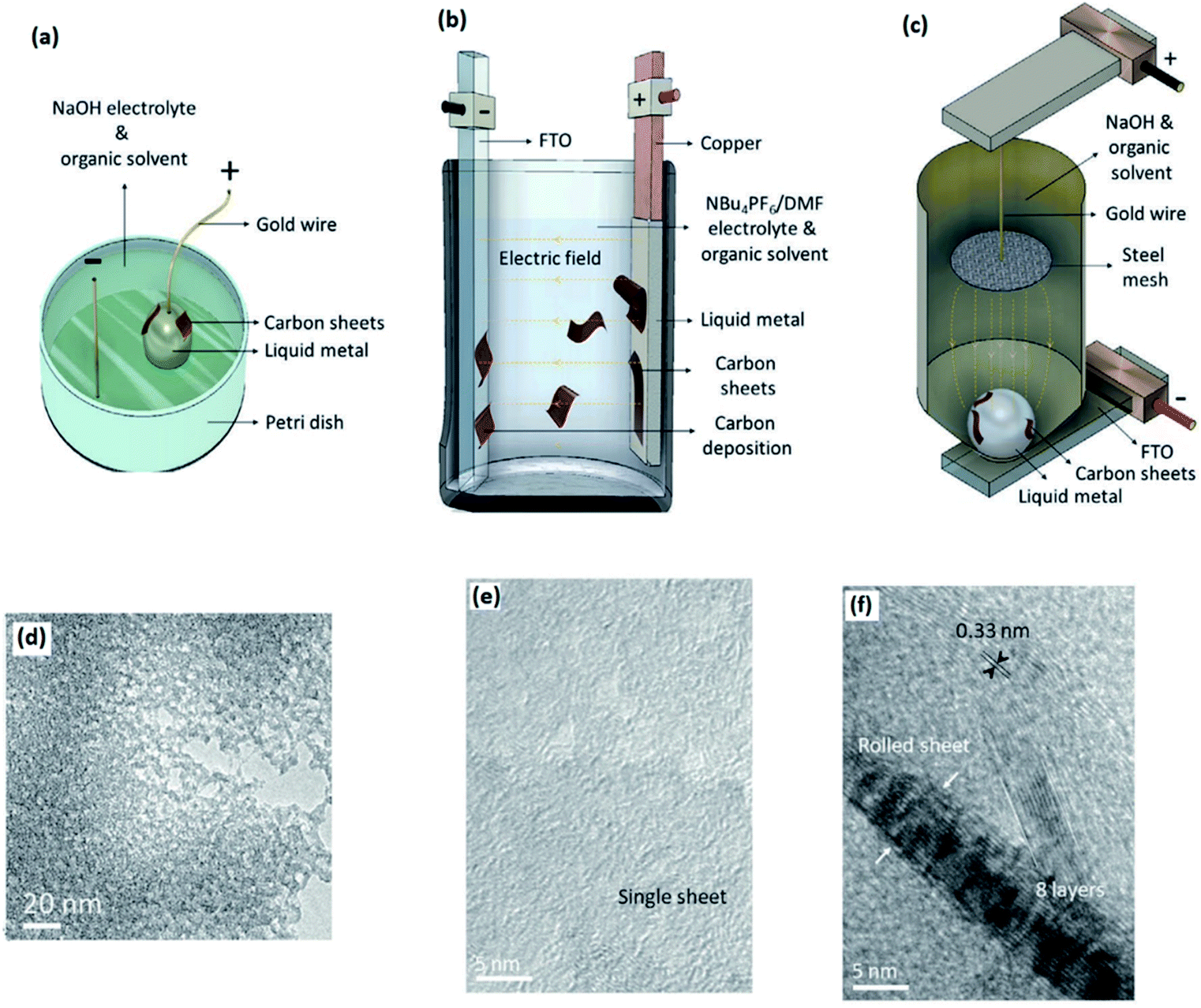
3.3.1.7 2D graphitic materials. Liquid metal was recently found to be a promising class of catalytic electrodes acting as an ultra-smooth platform for the electrochemical synthesis of 2D graphitic materials (2D-GMs) from liquid organic precursors.169 The outstanding conductivity of liquid metals makes them suitable conducting electrodes to carry out successful redox reactions. The ultimately smooth surface of liquid alloys combined with their non-polar nature made for a reliable planar substrate for further growth of 2D films. The natural catalytic properties of liquid metals promote the formation of C–C bonds on their surface. In summary, the interfacial characteristics of liquid metal surfaces facilitate the breaking of C–O, C–N, and C–H bonds in organic molecules of precursors which can then be followed by their reconstruction in other forms of graphitic C–C structures.169 Recent studies have demonstrated that the formation and adsorption of radicals on the surface of a liquid gallium alloy are more likely to occur in the presence of alloying elements and dopants. It was found that the activation barrier for dehydration of the graphene edge on the gallium alloy surface is lower than that for non-alloyed liquid metals.169 This ensured the employment of gallium based liquid metals as a unique platform for growth of 2D-GMs. To this end three different electrochemical cell configurations with liquid metal electrodes were established to synthesize 2D-GMs. The first cell contained an anodic aqueous system, the second cell contained an anodic non-aqueous system and the last cell contained a cathodic aqueous solution, respectively. Various organic solvents were employed in these cells as the carbon source. In the first configuration (Fig. 16a), the anodic direct potential was applied on the liquid metal droplet causing a potential gradient across the liquid metals and changing the charge distribution on the surface. This enabled Marangoni flow and resulted in turbulence on the surface of the liquid metal. Then the synthesized 2D-GMs were “self-exfoliated” by changing the direction of applied voltage. In the second configuration (Fig. 16b), a copper coil painted with liquid metal and another fluorine tin oxide (FTO) were employed as the electrolyte cell electrode. 2D-GMs were formed on the surface of liquid metals and then self-exfoliated and travelled to the FTO electrode by applying an anodic potential between 0.8 and 1.1 V.169 In the third configuration (Fig. 16c), the galinstan droplet is positioned on the FTO cathode dipped in a NaOH and organic mixture, while a steel mesh connected to an upper anode electrode was also floated inside the liquid mixture. The graphite materials were synthesized and floated in cathodic aqueous solution after applying the cathodic potential (−0.60 to −0.90 V).169 The materials characterization revealed that the carbon nanostructures synthesized using the first electrochemical cell configuration have a planar structure containing apparent porosities with nano-meter sizes. The HRTEM studies also revealed the amorphous nature of synthesized 2D-GNs with distinguished planes (Fig. 16d) with a measured thickness of approximately 1.5 nm. However, the synthesized 2D-GNs of the second cells had pinhole-free crystalline structures with typical six-fold symmetry with an interlayer spacing of 0.33 ± 0.01 nm (Fig. 16e and f). These nanosheets can be composed of a few 2D-GNs with an interlayer spacing of 0.33 nm. The accumulation of 8 layers of 2D-GNs is presented in Fig. 16f. In the third configuration, the cathodic potential yielded the development of graphene oxide nanosheets with a thickness of 2.7 nm.169
3.3.1.8 Sonochemically functionalized Ga2O3 2D films. The surface properties of 2D materials can be fundamentally altered and improved by the employment of surface functionalization techniques. Surface functionalization approaches offer a unique platform for synthesis of advanced functional 2D materials for a wide range of electronic applications.170–174 The 2D surface oxide of liquid metals as one of the natural sources of 2D materials can also be functionalized via sonochemical-assisted reactions to finally synthesize ultra-thin functionalized Ga2O3 nanosheets with controllable electronic and optoelectronic properties. For example, in a recently developed technique, the sonochemical assisted functionalization of liquid metal nanoparticles with selenium and silver nanostructures led to a tangible improvement in the visible light sensitivity of Ga2O3 nanosheets.175 The continuous sonochemical assisted synthesis of galinstan nanoparticles in an aqueous solution containing Ag and Se ion species led to the development of both functionalized galinstan nanoparticles and extracted Ga2O3 nanosheets.175 During sonication, the galinstan alloy flowed freely under mechanical loads and formed spherical particles (Fig. 17a). The surface oxide films on the galinstan droplet were delaminated during the sonication process and then were extracted from the sonochemically dispersed aqueous solution. Apart from the delamination and separation of surface oxide nanosheets, ultrasonication has another important effect, which is functionalization of the surface oxide films of liquid nanoparticles via Se and Ag ion species. EDS studies showed the uniform distribution of alloying elements on the surface of liquid metal particles confirming the presence of Se and Ag on the functionalized surfaces (Fig. 17b).
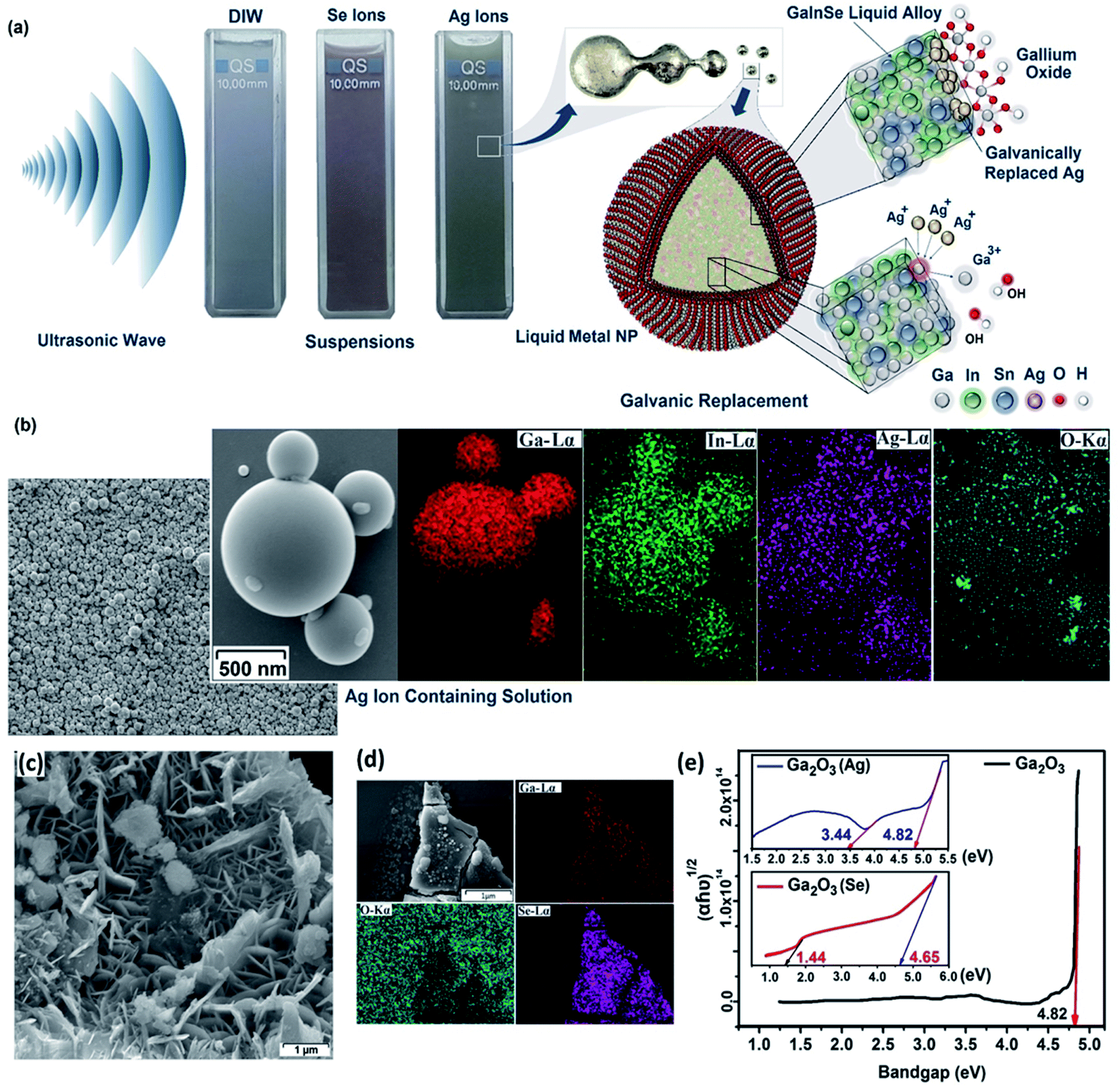 | ||
| Fig. 17 (a) The schematic of sonochemical-assisted synthesis of galinstan particles and their surface functionalization. (b) The EDS map of synthesized nanoparticles in aqueous solution containing ionic Ag. (c) FESEM image of the nanosheets. (d) The EDX elemental map analysis of the nanosheets. (e) Reflectance spectra of the nanosheets, accompanied by calculated bandgap values of the corresponding nanosheets. Reprinted with permission from ref. 175. | ||
The reported studies on extracted nanosheets from the sonochemical assisted functionalization technique demonstrated that the nanosheets are composed of gallium hydroxides (Fig. 17c). The following heat treatment at 400 °C facilitated the phase transformation of nanosheets from GaOOH nanosheets into Ga2O3. EDS analysis showed the uniform distribution of the alloying elements on the surface of Ga2O3 nanosheets (Fig. 17d). The presence of Ag and Se nanostructures on the surface of Ga2O3 nanosheets was attributed to the sonochemical assisted nucleation, growth and synthesis of Ag and Se nanostructures where the floating GaOOH nanosheets worked as the platform for nucleation of nanostructures. Raman studies also confirmed the functionalization of surface oxide nanosheets via Se and Ag elements. Specifically, the characterization of the Raman peaks of Ga2O3 nanosheets functionalized in Se ion containing solutions showed the nucleation of crystalline Se nanostructures and GaxSey compounds on the Ga2O3 nanosheets. It was found that the optical properties of Ga2O3 nanosheets were altered considerably. The optical bandgap of Ga2O3 nanosheets was altered and decreased from 4.82 eV in the UV region of the light spectrum to 3.44 eV for Ag functionalized Ga2O3 nanosheets and to 1.44 eV for Se functionalized Ga2O3 nanosheets, respectively (Fig. 17e).175 Therefore, sonochemical functionalization successfully altered the electronic properties of 2D surface oxides of liquid metals and alloys.
3.3.1.9 CuxO. Liquid metals with their unique surface properties can act as a template for growth of various kinds of nanostructured materials. The distinct interfacial chemistry of liquid metals has remained mostly unrealized and a majority of the interactions between liquid metal platforms and the surrounding ionic liquids still require further investigation.176 For instance, the templated synthesis of cupric oxide (CuO) on the surface of a gallium liquid alloy was explored and the mechanism of the room temperature synthesis of 2D CuO films was reported.177 In this study two approaches were employed to synthesize CuO nanostructures on the surface of galinstan droplets or particles (Fig. 18). In the first method, a droplet of a solution containing ionic Cu was drop cast on the surface of the galinstan droplet to facilitate the ionic interaction between the galinstan droplet and the surrounding ionic solution. To this end, the natural surface oxide of galinstan was initially removed by drop-casting of a 1.0 M NaOH solution on its surface for 2 min. The NaOH solution removed the natural Ga2O3 film from the surface of galinstan and a fresh surface of the InGaSn alloy was prepared for interaction with the ionic CuSO4 solution.177–180 For synthesis of CuO nanostructures various concentrations of NH4OH and CuSO4 solutions were sequentially added over the galinstan droplet. The process included the optimization of the pH of the solution for various concentrations of CuSO4 and various reaction times (Fig. 18a). The vdW delamination method was employed to separate the synthesized nanostructures from the surface of the galinstan droplet (Fig. 18b) for characterization studies.
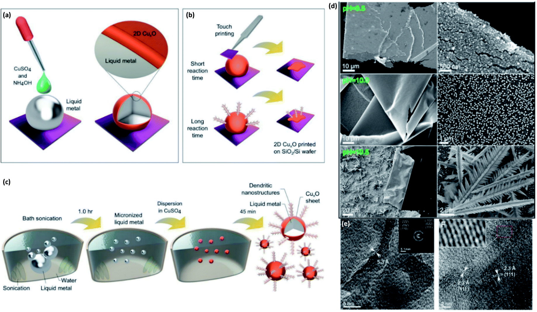 | ||
| Fig. 18 (a) The graphical scheme of the preparation of the surface of a galinstan droplet for growth of CuxO nanostructures by using a liquid containing CuSO4 solution. (b) The vdW delamination of CuxO nanostructures. (c) The sonochemical synthesis of galinstan nanoparticles in a dispersion containing CuSO4. (d) The morphology of CuxO nanostructures synthesized in solution with different pH contents. (e) The high resolution TEM image and HRTEM images from the basal planes or CuxO nanosheets exfoliated from the bulk liquid metals. Reprinted with permission from ref. 177. | ||
In the 2nd strategy, the galinstan droplet was sonicated and then transferred into a CuSO4 containing solution. The final products were micro- and nano-galinstan particles covered with CuxO nanostructures (Fig. 18c). It was found that the pH of the solution containing cupric ion species has a fundamental impact on the morphology and characteristics of the synthesized nanostructures. Different pH values have resulted in distinct phase transitions between CuO and Cu2O. It was found that the Cu2O content in the synthesized cupric oxide structures is dependent on the pH. Consequently, the pH directly affected the bandgap of nanostructured cupric oxides. It was established that the sample synthesized at pH 9.5 had an absorption edge at 629 nm corresponding to the bandgap of 1.98 eV which is close to the direct bandgap of Cu2O.181,182 The increase of pH up to 10, 10.5 and 11 occurred along with a bandgap decrease to the range of 1.16–1.17 eV, which was attributed to the formation of CuO nanostructures.183,184 The pH of the solution also has a direct impact on the morphology of synthesized cupric oxide films (Fig. 18d). It was observed that the delaminated nanostructures from the surface of the galinstan droplet usually have a flat and planar structure when the pH is chosen to be around pH 9.5. Furthermore, the long reaction time also led to the development and growth of nanostructures. It is possible to avoid secondary growth by limiting the reaction time. Thus 4.0 nm thick ultra-thin and smooth nanosheets of cupric oxide were synthesized. The HRTEM studies depicted that the wrinkled 2D nanosheets had a connected island morphology with a crystalline structure (Fig. 18e). The nanosheet thickness was found to be 5.3 Å (Fig. 18e). The HRTEM studies also confirmed that nanosheets are CuO with an interlayer spacing of 2.3 Å (Fig. 18f). Then, it was realized that the pH dependent properties of synthesized cupric oxide can be employed to synthesize different types of copper oxide products with various electronic properties. Altogether, the capability of liquid-phase assisted synthesis was established for synthesis of 2D cupric oxide films with desired tunable properties.
3.3.1.10 TiO2. 2D TiO2 films were synthesized by several different methods including top-down and bottom-up approaches. TiO2 has three dominant crystalline structures which are known as rutile (tetragonal), anatase (tetragonal) and brookite (orthorhombic) structures.185–187 The TiO2 crystalline structure is not intrinsically layered. Therefore, in reality exfoliation or isolation of the 2D TiO2 nanosheets is quite a challenging process. Recent reports show that the synthesized TiO2 nanosheets are almost in the form of small flakes or have polydisperse thickness with variable thicknesses.188–190 To tackle these challenges, the idea of the employment of liquid metals as a synthesis background for 2D TiO2 nanostructures was introduced.191 In this synthesis of 2D TiO2, a liquid metal based platform was employed to produce single layered nanostructures.191 To this end, a gallium titanium (Ga–Ti) alloy was prepared via grinding of micron sized titanium powders in liquid gallium using a mortar and pestle. The grinding breaks the Ti powders into small flakes which are then mixed together at a temperature of ∼80 °C until dissociation of all Ti powders occurs in the gallium alloy. The final alloy contains 1 wt% titanium. Then a gas injection technique was subsequently developed to synthesize TiO2 nanosheets (Fig. 19a). The liquid Ga–Ti alloy was submerged inside glass vials containing hydrochloric acid and deionized DIW (0.2 mol L−1; 5 mL). A continuous air flow stream inside the Ga–Ti alloy via a narrow glass nozzle guaranteed air bubble generation inside the Ga–Ti alloy. The expansion and following explosion of gas bubbles led to dispersion of oxide nanosheets in the dilute hydrochloric acid. Then, the hydrochloric acid dissolved the Ga2O3 nanosheets.192 After 30 min of the air injection process, the remaining nanosheets were collected and, after purification and washing, were used for characterisation.
 | ||
| Fig. 19 (a) The graphical scheme of preparation of TiO2 nanosheets. The gallium alloy containing 1 wt% Ti powder is mixed via a manual mortar-and-pestle grinding technique. The injection of gas bubbles inside the Ga–Ti alloy immersed in liquid solution (hydrochloric acid and deionized DIW) accompanied by subsequent filtration and purification of 2D TiO2 nanosheets. (b) The TEM image of wrinkled nanosheets accompanied by the (c) HRTEM image of the crystalline structure of 2D TiO2. (d) The AFM image and thickness profile of 2D TiO2 nanosheets. (e) The size distribution of 2D TiO2 nanosheets. Reprinted with permission from ref. 191. | ||
The characterization methods including Raman spectroscopy and XPS revealed that the remaining nanosheets are actually crystalline TiO2. The HRTEM studies on the extracted TiO2 films clearly demonstrated that 2D films possess an ultra-thin wrinkled nature (Fig. 19b). HRTEM also showed that the crystalline tetragonal structured TiO2 nanosheets have a dominant atomic layer spacing of 0.23 nm (Fig. 19c) with crystalline characteristics of rutile TiO2 (Fig. 19c).191,193 Further analysis of the surface morphology and thickness revealed that the synthesized rutile nanosheets had a thickness of 2.26 nm, corresponding to 3 to 4 unit cells of TiO2 (Fig. 19d). The subsequent measurements of the size and thickness distribution of nanosheets showed that these nanosheets had an average lateral size of 1.5 ± 0.2 μm (Fig. 19e). On the other hand, the investigation of the electronic structure of synthesized TiO2 nanosheets by TEM based electron energy loss spectroscopy (EELS) established that TiO2 nanosheets have a maximum dielectric constant of 24. Energy loss spectroscopy also showed that the synthesized 2D TiO2 nanosheets had a direct bandgap of 3.4 eV.190,194 Bandgap widening is detected in the case of synthesized 2D TiO2 nanosheets, which is expected to be due to the quantum confinement phenomenon.195 Consequently, the synthesis of novel 2D nanostructures was facilitated by the employment of the Cabrera–Mott oxidation phenomenon on the surface of liquid metals and alloys.191
3.3.2.1 GaPO4 semiconducting nanosheets. Gallium phosphate (GaPO4) is a semiconductor with a trigonal crystalline structure and cell parameters of a = 4.87 Å and c = 11.05 Å and γ = 120 Å, respectively (Fig. 20a and b).195,196 It has a high thermal stability up to 930 °C. The structure of GaPO4 has provided outstanding technical capabilities for this semiconductor material,196,197 for instance, piezoelectricity, which facilitates the mutual conversion of electrical energy or pulses into mechanical forces or oscillations. 2D GaPO4 synthesis was recently reported via a liquid metal-based synthesis approach.198,199 The piezoelectric GaPO4 does not naturally have a crystalline stratified structure, and hence the conventional mechanical exfoliation approaches do not work to produce 2D GaPO4 nanosheets. To tackle the limitation of synthesis of 2D GaPO4, a liquid metal-based technique was introduced based on vdW delamination and then employed where the naturally formed surface oxide of liquid Ga was used as a platform for the development of 2D GaPO4 films (Fig. 20c).199 The extracted surface oxide film of liquid metals was utilized later and employed in the secondary post-treatment technique.199 In this method, the 2D Ga2O3 films on the Si/SiO2 substrate were delaminated and then moved to the furnace for the secondary phosphatisation treatment (Fig. 20d). During heat-treatment H3PO4 powders are heated up at 350 °C and then the generated chemical vapour containing phosphorus is passed over the Ga2O3 film using N2 gas to react with the 2D film (Fig. 20d). For further characterization studies, the synthesized 2D films were kept inside a glovebox containing nitrogen.
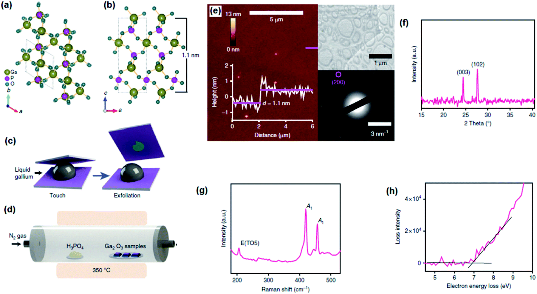 | ||
| Fig. 20 (a) The top view and (b) side view of GaPO4 demonstrating the out-of-plane structure of GaPO4. (c) The schematic of the vdW 2D printing of the Ga2O3 surface oxide of a gallium alloy. (d) The set-up for the secondary phosphatisation treatment. (e) The AFM thickness measurement of 2D GaPO4 shows the ultra-thin thickness of the film. The TEM studies show the crystalline structure of the 2D GaPO4 film. The (f) XRD and (g) Raman spectra of the 2D GaPO4 film. (h) The bandgap of the 2D GaPO4 film. Reprinted with permission from ref. 199. | ||
The fabricated 2D nanostructures were investigated by AFM, HRTEM and Raman techniques. The AFM studies confirmed the development of ultra-thin films with a 1.1 nm thickness, which is consistent with the unit cell dimensions of trigonal GaPO4 in the c crystalline direction (Fig. 20e).199 The investigation of the selected area electron diffraction (SAED) pattern of synthesized 2D films confirmed the growth of the crystalline GaPO4 structure with a lattice spacing of 0.21 nm corresponding to the d-spacing of the (200) plane of trigonal GaPO4 nanosheets (Fig. 20e). The XRD measurements also reaffirmed that the crystalline structure of the 2D GaPO4 film is dominated by the (003) and (102) planes of trigonal α-GaPO4 (ref. 199–202) (Fig. 20f). The Raman spectra of synthesized 2D nanosheets showed the characteristics peaks of tetrahedral PO4, which were attributed to the A1 vibration mode of crystalline phosphate (Fig. 20g). However, the characteristic peak of Ga2O3 was not observed demonstrating the successful conversion of Ga2O3 to the GaPO4 film after the phosphatisation process. Additional investigation into the optical properties demonstrated that the measured wide bandgap was about 6.9 eV for the 2D GaPO4 film, which is in excellent agreement with the previously reported values for the bandgap of GaPO4 films203–206 (Fig. 20h). Thus, all characterization studies verified the outstanding capability of this fabrication method for synthesis of 2D nanostructures which are not naturally available. As a result, the post-treatment on the surface oxide of liquid metals in a gaseous environment has also been found to be a reliable technique for fabrication of 2D based nanomaterials.
3.3.2.2 GaN and InN semiconducting nanosheets. It is noteworthy that liquid metals were also recently used for large-scale synthesis of ultra-thin 2D gallium nitride and indium nitride.207 The technique includes the post-ammonolysis treatment of the surface oxide of liquid metals, which enabled wafer-scale deposition of high quality 2D GaN and InN films. The technique consists of squeeze printing of a gallium droplet between Si/SiO2 substrates (Fig. 21a) resulting in vdW exfoliation of the 2D Ga2O3 film with an ultra-thin thickness of 1.4 nm.206 The ammonolysis process was conducted at 800 °C in the presence of urea to convert the ultra-thin Ga2O3 film into wurtzite GaN (Fig. 21b).207 After ammonolysis, the thickness of the ultra-thin film decreased down to 1.3 nm, which corresponded to three wurtzite GaN unit cells (Fig. 21c). The precise characterization of the grown GaN film reaffirmed the growth of GaN crystals with a 5.18 nm lattice constant along the crystalline direction of (001).207 For TEM studies, the 2D Ga2O3 film on the TEM grid was subjected to the ammonolysis reaction. It was found that the synthesized GaN has a crystalline structure with an interlayer spacing of 0.28 Å (Fig. 21d). The XPS investigation affirmed the substantial replacement of nitrogen with oxygen in the Ga2O3 structure after ammonolysis treatment. Though Ga–O and Ga–N have the same bond length, the complete removal of oxygen from 2D GaN films was not attainable even with high temperature processing. The optical bandgap measurements also confirmed the substantial decrease of the bandgap from ∼4.8 eV in the Ga2O3 film down to ∼3.5 eV in the 2D GaN film (Fig. 21e).207 This bandgap decrease is expected since the surface functionalization and substitution of nitrogen atoms in the 2D Ga2O3 film significantly altered the electronic properties of the 2D film. The reason for the bandgap decrease was also attributed to the upward shift of the valence band of the GaN film due to the hybridization of the O2p–N2p orbitals.207
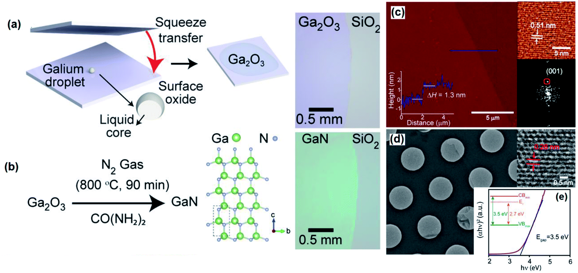 | ||
| Fig. 21 (a) The schematic of squeeze transfer of the surface oxide of gallium to the Si/SiO2 substrate. (b) The post-ammonolysis treatment for development of the 2D GaN film accompanied by the optical microscope image of the surface. (c) The AFM thickness profile of the film accompanied by (d) the HRTEM image of the crystalline structure of the GaN film. (e) The bandgap measurement of the 2D GaN film. Reprinted with permission from ref. 207. | ||
This technique was found as reliable method for the development of other types of 2D materials. Thus, researchers have investigated the direct conversion of the 2D In2O3 film of the surface oxide of a molten indium alloy into a 2D InN film. However, it was experimentally determined that the direct transformation of In2O3 into InN was not possible. Since InN is less stable than GaN and it undergoes decomposition to indium and nitrogen at temperatures above 650 °C and also faces morphological conversion, the direct conversion of 2D In2O3 into InN is not practically feasible.207–209 Thus, an intermediate bromination step was designed and utilized to effectively convert In2O3 into more reactive InBr3 nanosheets. To this end, liquid indium was used as the main material for the vdW exfoliation of 2D In2O3. The 2D In2O3 film was subjected to another post-bromination step which helped to transform 2D In2O3 into 2D InBr3. To fulfil the bromination process, the 2D In2O3 on the Si/SiO2 substrate was exposed for 20 s to HBr gas. The 2nd step was the ammonolysis process on InBr3 nanosheets to convert them into InN. Urea was employed at 630 °C as the NH3 source to facilitate nitrogen incorporation and replacement into the InBr3 structure.207
The homogeneous incorporation of nitrogen atoms into the structure of InBr3 was verified using characterization techniques. The characterization studies showed that crystalline InN with wurtzite structures and high stoichiometry developed along the substrate with a lattice constant of 5.5 Å.207 The subsequent bandgap measurements confirmed the capability of functionalization of 2D films by the two step synthesis approach. For example, a bandgap of 3.5 eV was recorded for the developed 2D InN film. Generally, the post-treatment was realized as a practical approach towards fabrication of advanced 2D materials when their synthesis requires the employment of expensive vacuum deposition methods.210–216 Subsequently, the developed 2D films were successfully employed in novel electronic and optoelectronic devices.207
3.3.2.3 SnS semiconducting 2D films. 2D materials with their high planar integrity and stiffness are capable of withstanding extremely large levels of strain during their working life. The crystalline nature of 2D materials allows them to be an excellent option for use in stress and strain related applications similar to piezoelectric and generator devices which are used for harvesting energy from mechanical stimuli in the surrounding environments.217–221 Apart from the amazing capabilities of piezoelectric materials, the technical limitations for fabrication of large-scale 2D materials with piezoelectric properties for application in functional instruments is still a big obstacle for development of reliable 2D-based piezoelectric devices. It is highly challenging to develop high quality 2D films with the shortest and lowest grain boundaries across the film to generate high voltage and current response.
In group IV of the periodic table, SnS is one of the mono-chalcogenides which has the potential to be selected as the material with favourable semiconductor and piezo-electrical properties.222,223 However, the wafer-scale synthesis of 2D SnS films still faces serious obstacles. Mechanical exfoliation techniques generally failed to produce 2D films with large-scale lateral dimensions with conformal thickness. Thus these techniques enable us to ensure fabrication of wafer-scale 2D piezoelectric films of reasonable quality.224–226 Furthermore, the chemical and vapour deposition based techniques, which are known as capable techniques for wafer-scale synthesis of ultra-thin films, produced films containing high frequencies of grain boundaries which are not favourable for most electronic applications.227 As an alternative approach, the liquid metal substrate can be a natural source for synthesis of novel 2D materials. However, vdW exfoliation of the surface oxide of liquid metals so far resulted in the formation of stacked 2D nanostructures with small lateral dimensions. Therefore, the practical applications of exfoliated 2D films of liquid metal for energy harvesting suffered the same limitations arising from their lateral dimensions since the piezoelectricity and power generation characteristics are based on the expansion of stress along the 2D lateral faces.227,228 Furthermore, the most serious obstacle for synthesis of monolayer SnS and other 2D mono-chalcogenide sulphides of group IV originated from the strong inter-layer interactions between the lone pair electrons of sulphur atoms, which is the considerably stronger bonding compared with the bonding strength in the VdW forces.228
Nevertheless, a liquid metal based synthesis approach was recently developed to grow large-scale homogeneous 2D SnS films.228 In this technique the fresh surface of liquid tin is subjected to an anoxic atmosphere containing 50 ppm H2S gas mixed in N2 at a temperature of 350 °C (Fig. 22a). The self-limiting Cabrera–Mott reaction resulted in the formation of a sulphide skin film on the surface of molten tin. The following vdW exfoliation enabled the transfer of the sulphide skin film over the molten tin to a desired substrate (Fig. 22a). The high surface tension of liquid metal ensured almost ideal growth at interfaces, leading to the growth of 2D films with minimum grain boundaries and dislocations.228–230 The study on the morphology of synthesized nanosheets showed the pin-hole free characteristics and the large lateral dimensions of the extracted SnS films (Fig. 22b). The HRTEM characterisation presented the crystalline nature of the developed SnS film with a 0.29 nm d-spacing matched to the (101) plane of the SnS crystalline film (Fig. 22c). A minimal number of grain boundaries was found in the microstructure of 2D planar films. Further TEM studies revealed the presence of micro-crystalline domains with a low concentration of grain boundaries throughout the developed 2D SnS film (Fig. 22d). The Raman spectra of the SnS film (Fig. 22e) also showed the characteristic vibration mode of the SnS film, confirming the development of selenium sulphide at the surface of galinstan after reaction with a sulphur containing atmosphere. Investigation of the morphology of the SnS film by AFM demonstrates the development of an ultra-thin film with a 0.7 nm thickness, which is matched to the unit-cell of monolayer SnS (Fig. 22f). The measured bandgap of the SnS monolayer was ∼1.4 eV, which is fairly matched to the theoretically calculated bandgap of the SnS monolayer.230,231 Generally, the large-scale synthesis of the crystalline monolayer SnS semiconductor was achieved via the vdW exfoliation of the synthesized 2D nanosheets on the surface of the tin alloy in the H2S environment.228
 | ||
| Fig. 22 (a) The schematic depiction of the synthesis process of the monolayer SnS film via interaction of liquid tin with H2S gas. (b) The TEM image depicts a monolayer SnS film (scale bar 500 nm). (c) The HRTEM image of crystalline SnS nanosheets with a d-spacing of 0.29 nm related to the plane of (101); the scale bar is 5 nm. (d) The dark-field TEM image of monolayer SnS depicts the minimal number of grains in the structure; the scale bar is 100 nm. (g) The AFM image accompanied by (f) the thickness profile of the monolayer SnS film. (e) The Raman spectra of the 2D SnS film. Reprinted with permission from ref. 228. | ||
3.3.2.4 Ga2S3 semiconducting 2D films. 2D post-transition-metal chalcogenide semiconductors are recognized as advanced functional materials with applications in topological insulators, transistors and sensors. Ga2S3 is a p-type semiconductor which has been developed previously with a nanometre scale thickness using deposition techniques.232–237 The 2D Ga2S3 film was synthesized by the sulphurization of the surface oxide film of liquid gallium.236,237 In general, the Ga2O3 film was delaminated from the surface of liquid gallium in the ambient atmosphere. Then, a washing process was employed to remove the remaining liquid metal droplets from the surface of the substrate. After this, a direct sulphurization technique inside the tube furnace was used where the Ga2O3 nanosheets were subjected to sulphur gas at 600 °C (Fig. 23a).237
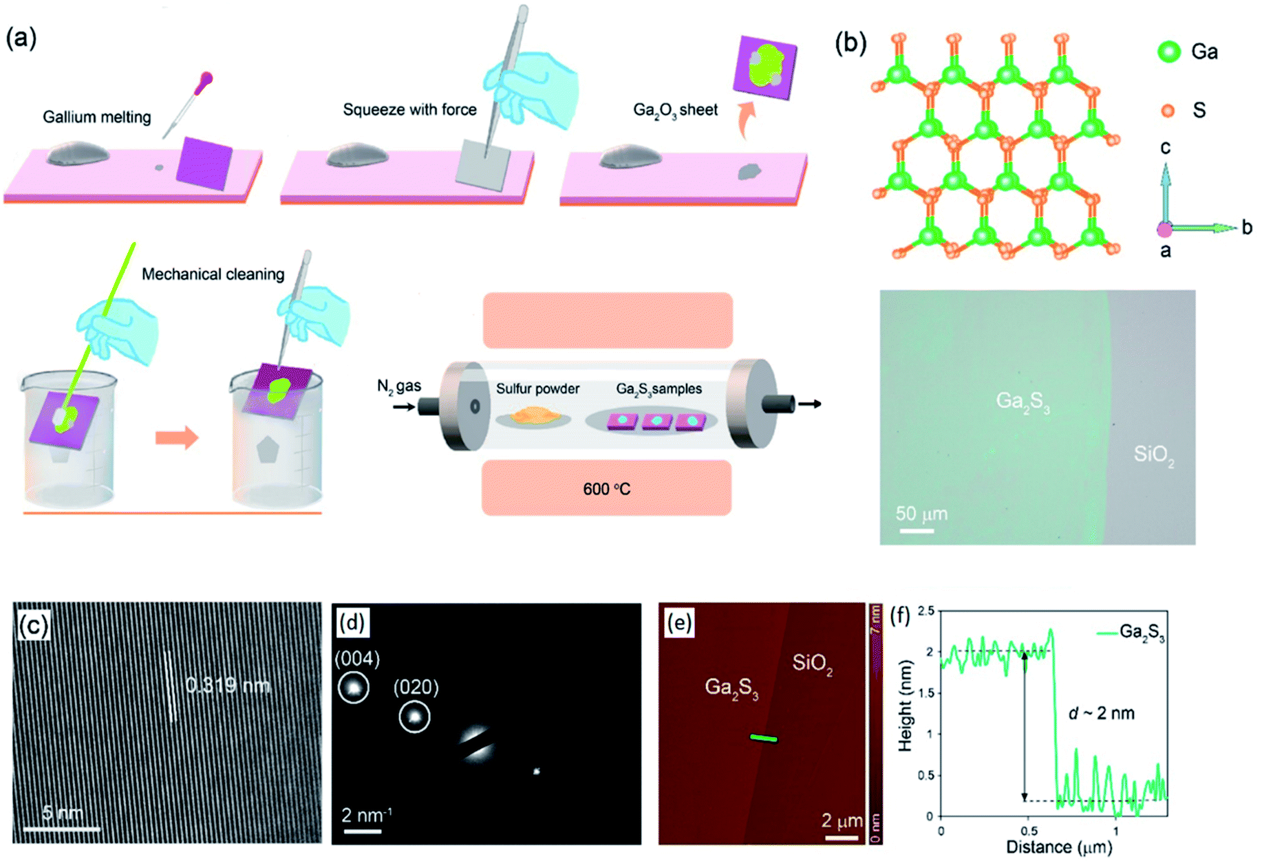 | ||
| Fig. 23 (a) The schematic representation of the synthesis of vdW delaminated Ga2S2 nanosheets. The direct sulfurization set up for the synthesis of Ga2S3 by using a quartz tube furnace at 600 °C. (b) The crystalline structure and optical image of synthesized Ga2S3 nanosheets. (c) The HRTEM and (d) SAED pattern of Ga2S3 nanosheets. (e) The AFM image accompanied by (f) the thickness profile of 2D Ga2S3 nanosheets. Reprinted with permission from ref. 237. | ||
The characterisation studies showed the development of the ultra-thin pin-hole free 2D Ga2S3 film over the Si/SiO2 substrate after the annealing treatment (Fig. 23b). For further characterization, the surface oxide of galinstan was delaminated on the surface of a TEM grid (Si3N4) followed by the direct sulphurization process. The HRTEM studies confirmed the single crystal structure of 2D Ga2S3 with an interlayer d spacing of 3.19 Å. This dimension is consistent with the crystalline (020) plane of α-Ga2S3 (Fig. 23c and d).237 Further studies on the crystallinity of the synthesized 2D Ga2S3 film confirmed the crystalline nature of films. The corresponding selected area electron diffraction (SAED) pattern showed that monoclinic α-Ga2S3 structures with crystalline (020) and (004) planes were developed during the sulphurization process.237 Additional characterization by micro-Raman spectroscopy also exhibited the characteristic vibration modes of GaS4 and Ga2S3 bonds for the tetrahedral corner of the GaS3 structure. Photoluminescence spectroscopy depicted a major broad peak at 640 nm corresponding to an average bandgap of 2.1 eV.236 The following AFM studies confirmed the deposition of a conformal pinhole free film with a 2.0 nm thickness and lateral dimensions of several micrometres (Fig. 23e and f).237
3.3.2.5 Bi2S3 semiconducting 2D films. The large area synthesis of 2D materials with high in-plane anisotropy is highly challenging since the synthesis of these anisotropic crystalline structures requires the correct selection of suitable platforms and substrates for growth of fragile crystalline 2D films. A liquid metal based synthesis approach was employed to synthesize ultra-thin bismuth oxide films from molten bismuth.238 In this method, the bismuth metal was initially melted inside a glovebox containing a constant flow of N2 gas. The molten bismuth alloy was then exposed to ≈100 ppm O2 to facilitate the Cabrera–Mott oxidation in a controlled oxygen environment. The 2D oxide films of Bi2O3 were delaminated and transferred to an appropriate substrate (Si/SiO2) via vdW exfoliation (Fig. 24a). To convert the Bi2O3 films to Bi2S3, a tube furnace was used containing elemental sulphur and N2 gas at a temperature of 450 °C for 15 min.238 The following characterization process confirmed the development of ultra-thin 2.5 nm thick Bi2S3 nanosheets (Fig. 24b). The HRTEM studies showed the development of 2D Bi2S3 films with a van der Waals string type crystalline structure with significant in-plane anisotropy. A typical crystal spacing of 3.2 Å was observed which is characteristic of the crystalline Bi2S3 material (Fig. 24c). The characterization studies also revealed the p-type nature of the developed 2D Bi2S3 film with a direct bandgap of 2.3 eV. Photoluminescence spectroscopy studies confirmed the effect of sulfur impurities on the PL emission. The studies showed a broad PL spectrum which was associated with the involvement of multiple transitions and the presence of surface trap-states. It was also found that the PL properties of the synthesized Bi2S3 film were a thickness-dependent factor.238
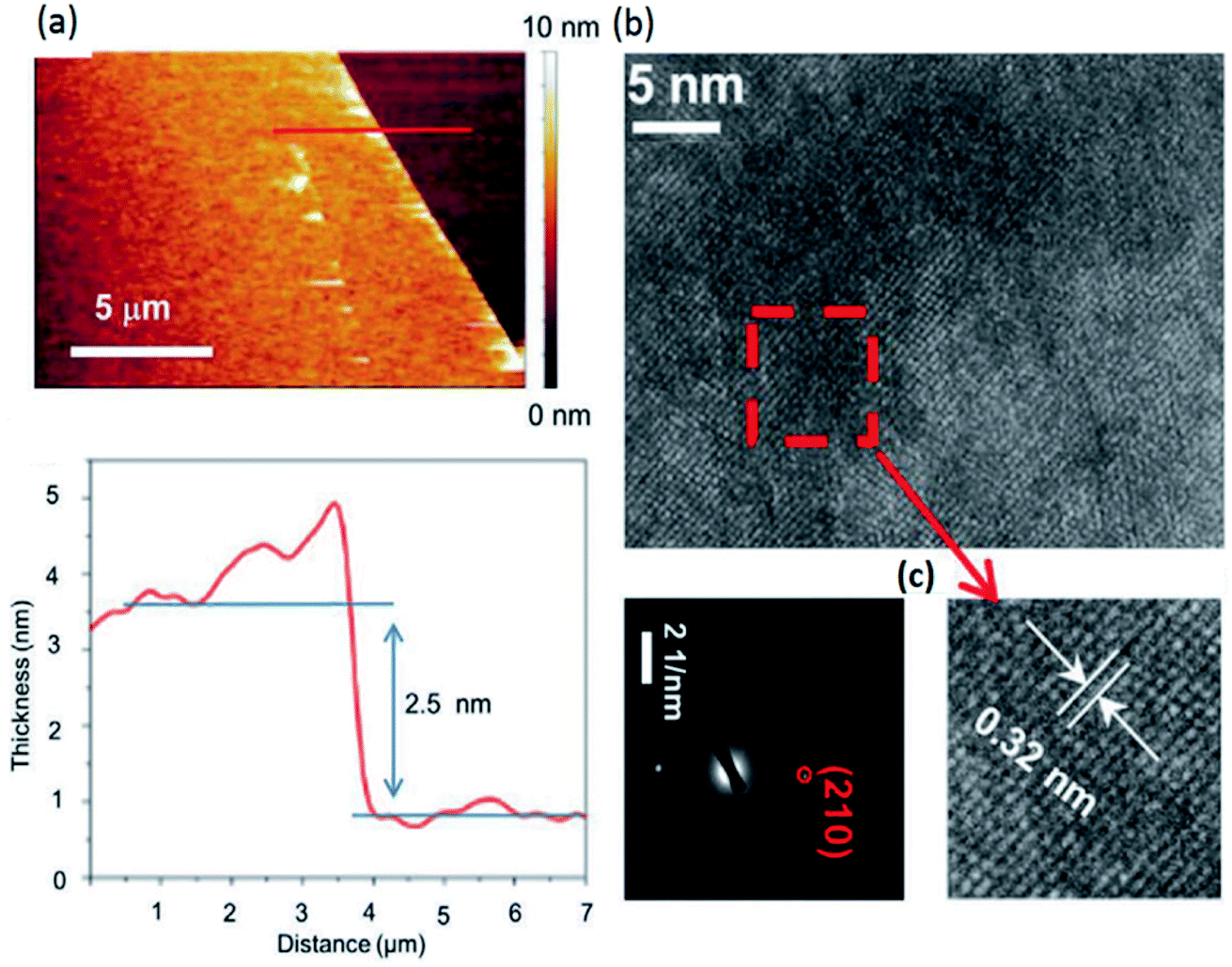 | ||
| Fig. 24 (a) The AFM image and thickness profile of the 2D Bi2S3 film. (b) The HRTEM image of the crystalline 2D Bi2S3 film. (c) The crystalline plane of (210) with an interlayer spacing of 0.32 nm is characterized.238 | ||
3.3.2.6 In2S3 semiconducting 2D films. The successful interaction of natural surface oxide films of liquid metals with the gaseous environment can be used to develop different types of 2D materials. In this concept, the atomic-scale thick 2D surface oxide film of a liquid indium alloy is employed for a further post-processing stage to synthesize 2D In2S3 films.239 Wafer-scale synthesis of ordered-vacancy tetragonal In2S3 ultra-thin nanostructures with the thickness down to the single unit cell limit is highly interesting since it enables the development of novel electronic and optoelectronic devices. In2S3 is not a layered material, and thus the large-area synthesis of the ultra-thin crystalline 2D In2S3 film is a challenging process. In an innovative approach, indium was melted at 180 °C inside a glovebox.239 The oxygen concentration was kept at less than 100 ppm. Before the delamination of the surface oxide film of indium, the natural surface oxide was removed prior to delamination of the fresh indium oxide film from the surface of molten indium. The pre-heated Si/SiO2 film was employed as a substrate to extract the fresh 2D In2O3 films. The printed In2O3 film was later transferred to a furnace and heated up to 350 °C and 450 °C for 15 min and exposed at the same time to sulphur gas via nitrogen as a transfer agent.239
The materials characterization studies confirmed the development of crystalline 2D In2S3 films with ultra-thin thickness. The uniformly developed In2O3 film had a 2.5 nm thickness confirmed by AFM studies (Fig. 25a and b). The studies by high-angle annular dark-field scanning transmission electron microscopy (HAADF-STEM) confirmed the development of the unique crystalline structure with well-ordered structural indium vacancies (Fig. 25c). Further studies via the annular dark field (ADF) showed that the periodic atomic peaks are separated by 0.6 nm and are ascribed to the stacked In1–S3 and In2–S3 atoms in the layered 2D structure (Fig. 25d). This 2D material showed a highly dispersive conduction band with estimated and measured low effective electron mass. These specific microstructural characteristics facilitated the development of ultra-thin 2D nanostructures with multiple band-like electronic transport channels which are sandwiched within a crystalline structure. In this unique configuration, the sandwiched conduction channel within the surrounding crystalline layer is less influenced by the surface conditions. Generally the technique was found to be a successful approach for large-area development of 2D semiconductor films. These sandwich-like 2D films are potentially less influenced by the inherently grown surface defects during the conventional wafer-scale synthesis of 2D semiconductor films. This is a highly important achievement in the wafer-scale development of novel 2D nanostructures for advanced electronic devices.
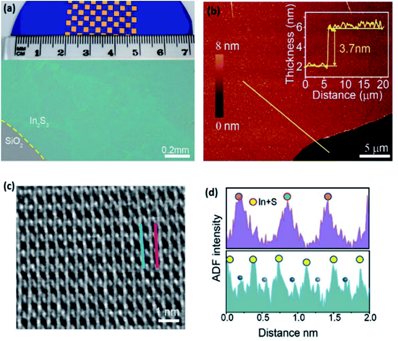 | ||
| Fig. 25 (a) The wafer-scale development of 2D In2S3 films with (b) an ultra-thin uniform thickness of 3.7 nm. (c) The HRTEM image shows the atomic-scale resolution image of the 2D In2S3 film. (d) The ADF analysis which shows the interlayer spacing of periodic layers. Reprinted with permission from ref. 239. | ||
4. Applications of 2D films of liquid metals
2D surface oxides of liquid metals are found to be functional materials with high capabilities and distinguished properties. The large-scale vdW exfoliation of 2D surface oxides and the post-processing treatment enabled the synthesis of novel 2D materials with considerable lateral dimensions and distinguished physical and chemical characteristics. The large-scale synthesis has provided the opportunity for application of these types of functional 2D materials in novel electronic instruments. While tremendous attention has been devoted to the electronic applications of 2D surface oxides of liquid metals, there are still a considerable number of environmental and sensing applications which are developing day by day. The next section reviews the latest reported functional applications of 2D surface oxide films of liquid metals and alloys in functional devices.4.1 Electronic applications
4.2 Catalytic and environmental applications
4.3 γ-AlOOH membrane
2D γ-AlOOH nanosheets were synthesized by interaction of the aqueous environment and water steam with the gallium alloy containing aluminium element. The synthesised 2D γ-AlOOH nanosheets were used to develop a membrane with photocatalytic activity.140 To this end, γ-AlOOH nanosheets were used to separate heavy metals and heavy oil emulsions from water. A ultra-high ion filtration capacity of 8.4 × 10⁴ L m−2 h−1 bar−1 was measured for γ-AlOOH. The high ion filtration capacity of 2D γ-AlOOH nanosheets was related to the capability of wrinkled and distorted γ-AlOOH films. These highly wrinkled nanostructures allowed the facile permeation of water molecules among the layered 2D γ-AlOOH nanosheets.140 The other main filtration mechanism of 2D γ-AlOOH nanosheets was related to the development of layered double hydroxide (LDH) between the 2D nanostructures and metal cations in water.140 The electrostatic attraction of metal cations to the surface of hydroxide groups of 2D γ-AlOOH films was another mechanism of the photocatalytic activity of the synthesized γ-AlOOH membrane.4.4 CuO based photocatalyst
A core–shell structure based on copper oxide/liquid metal was developed and demonstrated photocatalytic activities under solar light radiation. The ultrasonic dispersion of galinstan droplets in a solution containing CuSO4 films resulted in the formation of nanostructured materials based on CuO ultra-thin films or CuO dendritic structures fabricated on the surface of the galinstan alloy.177 The bandgap of CuO was measured to be 1.16 eV.177 Such a combination of low bandgap and the large surface of 2D oxide films on the surface of prepared liquid metal is considered an ideal condition for photocatalytic applications. The composite nanosheets exhibited superior photocatalytic performance for the degradation of the dye methylene blue with more than 90% dye degradation under a solar light simulator. The developed technique for synthesis of metal core/2D oxide nanostructured materials was found to be a reliable approach for synthesis of functional devices based on 2D surface oxides of liquid metals.4.5 SnOx for Co2 reduction
The amorphous SnOx 2D films decorated with Bi nanoparticle compounds and single atoms were found to be highly capable nanostructures for electrocatalytic reduction of CO2.139 Tin and bismuth are both recognized for their efficient role in degradation of CO2.138 It was found that the amorphous SnOx decorated with BiOx species (including nanoparticles and single atoms) can be used as electrocatalysts to effectively turn CO2 gas into formic acid (HCOOH) with a faradaic efficiency of more than 90% with stable performance during 10 h of electrocatalytic reactions.139The natural formation, ultra-thin nature, pin-hole free structure and considerable lateral dimensions of the synthesized surface oxide films accompanied by the facile vdW delamination of them on the desired substrate provided a great platform for successful synthesis of a novel generation of 2D materials and related electronic devices. Table 2 provides representative information on recently developed 2D materials and devices based on 2D surface oxide films of liquid metals and alloys.
| 2D film | Based alloy | Synthesis method | Specifications | Application | Ref. |
|---|---|---|---|---|---|
| Ga2O3 | Gallium, galinstan (EGaInSn) | vdW exfoliation (touch printing), gas injection in aqueous media | Crystalline (exfoliation), amorphous (gas injection) | High-bandgap semiconductor, insulator | 82 |
| Al2O3 | Galinstan–Al | vdW exfoliation (touch printing), gas injection in aqueous media | Crystalline (exfoliation), amorphous (gas injection) | High-bandgap semiconductor, insulator | 82 |
| Gd2O3 | Galinstan–Gd | vdW exfoliation (touch printing), gas injection in aqueous media | Crystalline (exfoliation), amorphous (gas injection) | High-bandgap semiconductor, insulator | 82 |
| HfO2 | Galinstan–Hf | vdW exfoliation (touch printing), gas injection in aqueous media | Crystalline (exfoliation), amorphous (gas injection) | High-bandgap semiconductor, insulator | 82 |
| SnO | Tin (Sn) | vdW exfoliation (touch printing) | Crystalline, p-type, ambipolar characteristics | Field effect transistor | 93 |
| SnO, SnO2, Sn2O3 | Tin (Sn) | vdW exfoliation (touch printing) | Crystalline, mixture of SnO, SnO2 and Sn2O3, n-type, p-type | — | 106 |
| Bi2O3 | Bismuth | vdW exfoliation (touch printing), oxidation in a controlled atmosphere | Crystalline | UV-A and UV-B photodetector | 107 |
| SnO/In2O3 | Tin (Sn)–indium (In) | Sequential vdW exfoliation (touch printing) | Crystalline, p–n heterojunction | UV and visible light phototransistor | 116 |
| GaS | Gallium | Screen printing, sequential low-temperature phase transformation of Ga2O3 to GaCl3 to GaS | Crystalline | FET and phototransistor | 119 and 123 |
| ITO | Indium-5 at% tin | Squeeze printing | Crystalline, monolayer and bilayer on a flexible substrate | Flexible capacitive touch screen | 128 |
| CoOx | Galinstan–Co | Gas injection in aqueous media | Aqueous solution containing HCl | Electrocatalysis | 138 |
| SnOx | Tin–bismuth | Oxygen gas injection into a Sn–Bi alloy covered with non-aqueous solvents | SnOx amorphous nanoflakes and SnOx crystalline nanorods | CO2 reduction to formic acid | 139 |
| Al2O3 | Aluminium | Al interaction with the aqueous environment | Phase transformation of crystalline γ-AlOOH into Al2O3 | γ-AlOOH membrane for metallic ion separation | 140 |
| MnO2 | Gallium–indium (EGaIn) | Galvanic replacement of galinstan particles with MnO4− | Metallic core/2D MnO2 shell, crystalline | Photocatalysis | 166 |
| MoSx | Galinstan | Cathodic reaction in aqueous solution containing (NH4)2MoS4 | Crystalline | — | 168 |
| 2D-GMs | Galinstan | Electrochemical cell | 2D carbon based materials | — | 169 |
| Ga2O3 (Ag, Se) | Galinstan | Galvanic replacement/functionalization of 2D Ga2O3 with Ag and Se ions | Nanosheets | UV and visible light photodetector, heterojunction | 175 |
| CuxO | Galinstan | Chemical interaction of galinstan in NH4OH + CuSO4 solution | Morphology dependence on pH content (from crystalline nanosheets to dendrites) | Photocatalysis | 177 |
| TiO2 | Gallium–Ti | Metal alloying, gas injection in aqueous media | Crystalline, wrinkled nanosheets | — | 191 |
| GaPO4 | Gallium | vdW exfoliation (touch printing), reaction with phosphorus at 350 °C (N2 + H3PO4) | Crystalline | Piezoelectric | 199 |
| GaN | Gallium | vdW exfoliation (touch printing), ammonolysis reaction | Crystalline, high carrier mobility of 21.5 cm2 V−1 s−1 | — | 207 |
| InN | Indium | vdW exfoliation (touch printing), bromination + ammonolysis reactions | Crystalline | — | 207 |
| SnS | Stanium | vdW exfoliation (touch printing), reaction with H2S at 600 °C | Crystalline | Piezoelectric nano-generators, broadband photodetectors | 228 and 258 |
| Ga2S3 | Gallium | vdW exfoliation (touch printing), reaction with H2S at 600 °C | Crystalline | Optical and gas sensor | 237 |
| Bi2S3 | Bismuth | vdW exfoliation (touch printing), reaction with H2S at 450 °C | Crystalline | Optoelectronic FET | 238 |
| In2S3 | Indium | vdW exfoliation (touch printing), reaction with H2S at 450 °C | Crystalline with a sandwiched structure | Transistor with high electron mobility | 239 |
| WS2/Ga2O3 | Galinstan | vdW exfoliation (touch printing), and transfer of the 2D Ga2O3 film on the surface of monolayer WS2 | Passivation of monolayer WS2via the glassy Ga2O3 2D film | Optoelectronic device | 259 |
5 Conclusions
The naturally occurring surface oxide films of liquid metals and alloys are recognized as remarkable and distinguished 2D nanostructured materials which are either not available as layered materials or require expensive high-vacuum synthesis techniques. The liquid state of liquid metals has provided a unique platform for conformal growth of their 2D surface oxide films when in contact with the atmosphere. The natural self-limiting formation of these 2D nanostructures accompanied by the lack of strong attachment bonding between them and their host alloy enabled the facile delamination of these 2D surface oxide films from their metal substrate. Thus, the vdW exfoliation and touch printing separations are among the most convenient techniques for delamination and subsequent deposition of 2D surface oxide films of liquid alloys on desired substrates. However, the synthesis techniques are not merely restricted to vdW delamination methods. Screen printing is another approach which was also found to be a capable technique for large-scale synthesis of 2D surface oxide films with large area. The extracted nanosheets are found in both amorphous and highly crystalline states, are defect free with an atomically thin thickness and have considerable lateral dimensions.The body content of this review is dedicated to the recently developed and synthesized functional 2D surface oxide films of liquid metals and alloys. In this context, various types of 2D oxide films of liquid metal and alloys including Ga2O3, Al2O3, Gd2O3, HfO2, SnOx, SnO2, Sn2O3, Bi2O3, In2O3, SnO/In2O3, ITO, MnO2, CoOx, CuxO, 2D-GMs and TiO2 are introduced and their characteristics are reviewed. The synthesized nanosheets have both crystalline and amorphous structures, and thus they are highly capable for development of advanced electronic devices for different functionalities. The post-synthesis treatment of 2D oxide films ensured the successful synthesis of novel non-oxide 2D semiconductors with outstanding properties. Several types of 2D films including GaS, Ga2S3, GaPO4, GaN, InN, MoSx, Bi2S3, In2S3, and SnS were synthesized by post-treatment of oxide films of liquid metals. The post-processing has also demonstrated great potential for development of advanced materials similar to vdW heterostructures, passivating layers and p–n heterojunctions.
In the framework of novel 2D materials and electronic devices, the rapid progress in this field ensures a promising future for development of novel devices based on 2D surface oxide films of liquid metals. In this concept, synergic improvement and development can be achieved by employment of different types of liquid metals and alloys. Further investigations on the effect of gaseous environments on the thermodynamic of growth of surface skin films of liquid alloys can tangibly affect the future trends for synthesis of novel 2D materials. Furthermore, the innovative functionalization techniques of 2D materials can enable us to synthesize novel 2D materials with unique and unprecedented properties. It should be admitted that the improvement of interfacial nano-engineering and surface functionalization methods can cause a paradigm shift in the development of novel electronic devices based on 2D semiconductor oxides of liquid metals.
Conflicts of interest
There are no conflicts to declare.Acknowledgements
This study was supported by the Research and Development Program of Ghent University Global Campus, South Korea.References
- G. Fiori, F. Bonaccorso, G. Iannaccone, T. Palacios, D. Neumaier, A. Seabaugh, S. K. Banerjee and L. Colombo, Nat. Nanotechnol., 2014, 9, 768–779 CrossRef CAS.
- E. Fortunato, P. Barquinha and R. Martins, Adv. Mater., 2012, 24, 2945–2986 CrossRef CAS.
- L. Wang and T. Sasaki, Chem. Rev., 2014, 114, 9455–9486 CrossRef CAS.
- M. Karbalaei Akbari and S. Zhuiykov, Nat. Commun., 2019, 10, 3873 CrossRef.
- M. Karbalaei Akbari, J. Hu, F. Verpoort, H. Lu and S. Zhuiykov, Nano-Micro Lett., 2020, 12, 83 CrossRef.
- M. Karbalaei Akbari and S. Zhuiykov, in Ultrathin Two-Dimensional Semiconductors for Novel Electronic Applications, ed. M. Karbalaei Akbari and S. Zhuiykov, CRC Press, Taylor and Francis, Boca Raton, 1st edn, 2020, ch. 8, pp. 275–307 Search PubMed.
- M. Karbalaei Akbari and S. Zhuiykov, in Ultrathin Two-Dimensional Semiconductors for Novel Electronic Applications, ed. M. Karbalaei Akbari and S. Zhuiykov, CRC Press, Taylor and Francis, Boca Raton, 1st edn, 2020, ch. 7, pp. 229–273 Search PubMed.
- M. Karbalaei Akbari and S. Zhuiykov, in Ultrathin Two-Dimensional Semiconductors for Novel Electronic Applications, ed. M. Karbalaei Akbari and S. Zhuiykov, CRC Press, Taylor and Francis, Boca Raton, 1st edn, 2020, ch. 6, pp. 171–227 Search PubMed.
- M. Karbalaei Akbari and S. Zhuiykov, in Ultrathin Two-Dimensional Semiconductors for Novel Electronic Applications, ed. M. Karbalaei Akbari and S. Zhuiykov, CRC Press, Taylor and Francis, Boca Raton, 1st edn, 2020, ch. 5, pp. 145–169 Search PubMed.
- S.-H. Bae, H. Kum, W. Kong, Y. Kim, C. Choi, B. Lee, P. Lin, Y. Park and J. Kim, Nat. Mater., 2019, 18, 550–560 CrossRef CAS.
- S. Milana, Nat. Nanotechnol., 2019, 14, 914–921 CrossRef.
- C. L. Tan, X. H. Cao and X. J. Wu, Chem. Rev., 2017, 117, 6225–6231 CrossRef CAS.
- K. S. Novoselov, F. Jiang and D. Schedin, et al. , Proc. Natl. Acad. Sci. U. S. A., 2005, 102, 10451–10453 CrossRef CAS.
- K. F. Mak, C. Lee and J. Hone, Phys. Rev. Lett., 2010, 105, 136805 CrossRef.
- G. R. Bhimanapati, Z. Lin and V. Meunier, et al. , ACS Nano, 2015, 9, 11509–11539 CrossRef CAS.
- S. Z. Butler, S. M. Hollen and L. Cao, et al. , ACS Nano, 2013, 7, 2898–2926 CrossRef CAS.
- Y. Liu, X. Duan, Y. Huang and X. Duan, Chem. Soc. Rev., 2018, 47, 6388–6409 RSC.
- A. Gupta, T. Sakthivel and S. Seala, Prog. Mater. Sci., 2015, 73, 44–126 CrossRef CAS.
- D. Akinwande, C. Huyghebaert, C. H. Wang, M. I. Serna, S. Goossens, L.-J. Li, H. S. P. Wong and F. H. L. Koppens, Nature, 2019, 573, 507–518 CrossRef CAS.
- F. Zhou, J. Chen, X. Tao, X. Wang and Y. Chai, Research, 2019, 1, 9490413 Search PubMed.
- Z. Sun, T. Liao and Y. Dou, et al. , Nat. Commun., 2014, 5, 3813 CrossRef CAS.
- Z. Cai, B. Liu and X. Zou, et al. , Chem. Rev., 2018, 118, 6091–6033 CrossRef CAS.
- W. Hao, C. Marichy and C. Juornet, 2D Mater., 2019, 6, 012001 CrossRef CAS.
- M. Karbalaei Akbari and S. Zhuiykov, in Ultrathin Two-Dimensional Semiconductors for Novel Electronic Applications, ed. M. Karbalaei Akbari and S. Zhuiykov, CRC Press, Taylor and Francis, Boca Raton, 1st edn, 2020, ch. 1, pp. 1–42 Search PubMed.
- M. Karbalaei Akbari and S. Zhuiykov, in Ultrathin Two-Dimensional Semiconductors for Novel Electronic Applications, ed. M. Karbalaei Akbari and S. Zhuiykov, CRC Press, Taylor and Francis, Boca Raton, 1st edn. 2020, ch. 2, pp. 43–77 Search PubMed.
- M. Yi and Z. Shen, J. Mater. Chem. A, 2015, 3, 11700–11715 RSC.
- H. Tao, Y. Zhang and Y. Gao, et al. , Phys. Chem. Chem. Phys., 2017, 19, 921–960 RSC.
- Y. Huang, Y. H. Pan, R. Yang and L. H. Bao, et al. , Nat. Commun., 2020, 11, 2453 CrossRef CAS.
- L. J. Ji, Y. Qin, D. Gui, W. Li, Y. Li, X. Li and P. Lu, Chem. Mater., 2018, 30, 8732–8738 CrossRef CAS.
- X. Cai, Y. Luo, B. Liu and H. M. Cheng, Chem. Soc. Rev., 2018, 47, 6224–6266 RSC.
- J. Yu, J. Li, W. Zhang and H. Chang, Chem. Sci., 2015, 6, 6705–6716 RSC.
- A. Mannix, B. Kiraly, M. Hersam and N. P. Guisinger, Nat. Rev. Chem., 2017, 1, 0014 CrossRef CAS.
- I. A. De Castro, A. F. Chrimes and A. Zavabeti, et al. , Nano Lett., 2017, 17, 7831–7838 CrossRef.
- M. G. Kanatzidis, R. Pottgen and W. Jeitschko, Angew. Chem., Int. Ed., 2005, 44, 6996–7023 CrossRef CAS.
- M. Song and M. D. Dickey, Room-temperature liquid metals as functional liquids, in Functional Organic Liquids, ed. T. Nakanishi, Wiley-VCH Verlag GmbH & Co. KGaA, 2019, pp. 251–271 Search PubMed.
- N. W. Ashcroft and J. Lekne, Phys. Rev., 1966, 145, 83 CrossRef CAS.
- G. Bo, L. Ren, X. Xu, Y. Du and S. Dou, Adv. Phys.: X, 2018, 3, 1446359 Search PubMed.
- T. Daeneke, K. Khoshmanesh and N. Mahmood, et al. , Chem. Soc. Rev., 2018, 47, 4073–4111 RSC.
- K. Kalantar-Zadeh, J. Tang and T. Daeneke, et al. , ACS Nano, 2019, 13, 7388–7395 CrossRef CAS.
- M. D. Dickey, ACS Appl. Mater. Interfaces, 2014, 6, 18369–18379 CrossRef CAS.
- A. Tabatabai, A. Fassler, C. Usiak and C. Majidi, Langmuir, 2013, 29, 6194–6200 CrossRef CAS.
- J. Yang, W. Cheng and K. Kalantar-Zadeh, Proc. IEEE, 2019, 107, 2168–2184 CAS.
- M. D. Dickey, Adv. Mater., 2017, 29, 1606425 CrossRef.
- Z. J. Farrell and C. Tabor, Langmuir, 2018, 34(1), 234–240 CrossRef CAS.
- S. Holcom, M. Brothers, A. Diebold, W. Thatcher, D. Mast, C. Tabor and J. Heikenfeld, Langmuir, 2016, 32(48), 12656–12663 CrossRef.
- J. Kim, F. Renb and S. J. Pearton, Nanoscale Horiz., 2019, 4, 1251–1255 RSC.
- Q. Xu, N. Qudalov, Q. Guo, H. Jaeger and E. Brown, Phys. Fluids, 2012, 24, 063101 CrossRef.
- R. D. Long and P. C. McIntyre, Materials, 2012, 5, 1297–1335 CrossRef CAS.
- S. Cho, J. Yu, S. K. Kang and D. Shih, JOM, 2005, 57, 50–52 CrossRef CAS.
- C. Gattinoni and A. Michaelides, Surf. Sci. Rep., 2015, 70, 424–447 CrossRef CAS.
- Q. Wang, Y. Yu and J. Liu, Adv. Eng. Mater., 2018, 20, 1700781 CrossRef.
- H. G. Deming, J. Chem. Educ., 1942, 19, 336 CrossRef CAS.
- G. R. Paranjpe and R. M. Joshi, J. Phys. Chem. A, 1931, 36, 2474–2482 CrossRef.
- T. W. Richards, H. L. Frevert and C. E. Teeter, J. Am. Chem. Soc., 1928, 50, 1293–1302 CrossRef CAS.
- C. Guminski and L. A. Zabdyr, J. Phase Equilib., 1992, 13, 401 CrossRef CAS.
- M. J. Q. Hernandez, J. A. Pero-Sanz and L. F. Verdeja, in Solidification and Solid-State Transformations of Metals and Alloys, Elsevier Science, Saint Louis, USA, 2017 Search PubMed.
- Y. Wu, Z. Deng and Z. Peng, et al. , Adv. Funct. Mater., 2019, 29, 1903840 CrossRef.
- W. B. Jensen, J. Chem. Educ., 2003, 80, 952 CrossRef CAS.
- L. J. J. Norrby, J. Chem. Educ., 1991, 68, 110–113 CrossRef CAS.
- V. Heine, J. Phys.: Condens. Matter, 1968, 1, 222 Search PubMed.
- O. Zuger and U. Durig, Phys. Rev. B: Condens. Matter Mater. Phys., 1992, 46, 7319–7321 CrossRef.
- S. C. Flower and G. A. Saunders, Philos. Mag. B, 1990, 62, 311–328 CAS.
- P. Cucka and C. S. Barrett, Acta Crystallogr., 1962, 15, 865–872 CrossRef CAS.
- Z. I. Tolmacheva and V. N. Eremenko, Powder Metall. Met. Ceram., 1963, 2, 369–376 CrossRef.
- T. J. Anderson and I. Ansara, J. Phase Equilib., 1991, 12, 64–72 CrossRef CAS.
- T. Liu, P. Sen and C. J. Kim, J. Microelectromech. Syst., 2012, 21, 443–450 CAS.
- S. Liu, K. Sweatman, S. McDonald and K. Nogita, Materials, 2018, 11(8), 1384 CrossRef.
- T. Ueno, E. Summers and T. Higuchi, Sens. Actuators, A, 2007, 137, 134–140 CrossRef CAS.
- S. P. Yatsenko, N. A. Sabirzyanov and A. S. Yatsenko, J. Phys.: Conf. Ser., 2008, 98, 062032 CrossRef.
- A. Preuss, B. Adolphi and T. Wegener, Anal. Bioanal. Chem., 1995, 353, 399–402 CrossRef CAS.
- L. Leontie, M. Caraman, M. Alexec and C. Harnagea, Surf. Sci., 2002, 507, 480–485 CrossRef.
- I. Filimonov and D. Luss, AIChE J., 2004, 50, 2287–2296 CrossRef CAS.
- R. Vargas, D. Carvajal, B. Galavis, A. Maimone, L. Madriz and B. R. Scharifker, Int. J. Photoenergy, 2019, 2019, 2571906 CrossRef.
- N. Cabrera and N. F. Mott, Rep. Prog. Phys., 1949, 12, 163 CrossRef CAS.
- K. Gelderman, L. Lee and S. W. Donne, J. Chem. Educ., 2007, 84, 685–688 CrossRef CAS.
- M. J. Regan, H. Tostmann and P. S. Pershan, et al. , Phys. Rev. B: Condens. Matter Mater. Phys., 1997, 55, 10786–10790 CrossRef CAS.
- Y. Wang, Y. Li, J. Zhang, J. Zhuang, L. Ren and Y. Du, Front. Chem., 2019, 7, 356 CrossRef CAS.
- M. J. Caturla, J. Z. Jiang, E. Louis and J. M. Molina, Metals, 2015, 5, 2128–2133 CrossRef CAS.
- M. Thirumoorthi and J. T. J. Prakash, J. Asian Ceram. Soc., 2016, 4, 124–132 CrossRef.
- P. Sen and C. J. Kim, IEEE Trans. Ind. Electron., 2009, 56, 1314–1330 Search PubMed.
- W. Zhang, B. S. Naidu and J. Z. Ou, et al. , ACS Appl. Mater. Interfaces, 2015, 7, 1943–1948 CrossRef CAS.
- A. Zavabeti, J. Z. Ou and B. J. Carey, et al. , Science, 2017, 358, 332–335 CrossRef CAS.
- D. Kim, et al. , ACS Appl. Mater. Interfaces, 2013, 5, 179–185 CrossRef CAS.
- D. R. Lide, in CRC Handbook of Chemistry and Physics, Internet Version, CRC Press, 85th edn, 2005 Search PubMed.
- V. Nicolosi, M. Chhowalla, M. G. Kanatzidis, M. S. Strano and J. N. Coleman, Science, 2013, 340, 1226419 CrossRef.
- J. N. Coleman, et al. , Science, 2011, 331, 568–571 CrossRef CAS.
- X. Zhao and D. Vanderbilt, Phys. Rev. B: Condens. Matter Mater. Phys., 2002, 65, 233106 CrossRef.
- W. E. Lee and K. P. D. Lagerlof, J. Electron Microsc. Tech., 1985, 2, 247–258 CrossRef CAS.
- M. A. Ballem, F. Söderlind, P. Nordblad, P.-O. Käll and M. Odén, Microporous Mesoporous Mater., 2013, 168, 221–224 CrossRef CAS.
- P. Thompson, D. E. Cox and J. B. Hastings, J. Appl. Crystallogr., 1987, 20, 79–83 CrossRef CAS.
- R. Pottgen, Z. Naturforsch., B: J. Chem. Sci., 2006, 61, 677–698 Search PubMed.
- J. Chena, L. Zheng and W. Yin, et al. , Phys. B, 2020, 599, 1412467 Search PubMed.
- T. Daeneke, P. Atkin and R. Orrell-Trigg, et al. , ACS Nano, 2017, 11, 10974–10983 CrossRef CAS.
- S. K. Sen, S. Sen and C. L. Bauer, Thin Solid Films, 1981, 82, 157–164 CrossRef CAS.
- P. De Padova, M. Fanfoni, R. Larciprete, M. Mangiantini, S. Priori and P. A. Perfetti, Surf. Sci., 1994, 313, 379–391 CrossRef CAS.
- A. J. Bevolo, J. D. Verhoeven and M. A. Noack, Surf. Sci., 1983, 134, 499–528 CrossRef CAS.
- E. Fortunato, R. Barros, P. Barquinha, V. Figueiredo, S. H. Park, C. S. Hwang and R. Martins, Appl. Phys. Lett., 2010, 97, 052105 CrossRef.
- Y. D. Kim and J. Hone, Nature, 2017, 544, 167–168 CrossRef CAS.
- H. Wang and A. L. Rogach, Chem. Mater., 2014, 26, 123–133 CrossRef CAS.
- K. Nomura, K. Kamiya, T. Hosono and H. Ambipolar, Adv. Mater., 2011, 23, 3431–3434 CrossRef CAS.
- S. H. Kim, I. H. Baek, D. H. Kim, J. J. Pyeon, T. M. Chung, S. H. Baek, J. S. Kim, J. H. Han and S. K. Kim, J. Mater. Chem. C, 2017, 5, 3139–3145 RSC.
- J. A. Caraveo-Frescas, M. A. Khan and H. N. Alshareef, Sci. Rep., 2015, 4, 5243 CrossRef.
- L. Y. Liang, H. T. Cao, X. B. Chen, Z. M. Liu, F. Zhuge, H. Luo, J. Li, Y. C. Lu and W. Lu, Appl. Phys. Lett., 2012, 100, 263502 CrossRef.
- L. Li, C. Zhang and W. Chen, Nanoscale, 2015, 7, 12133–12142 RSC.
- Z. Wang, P. K. Nayak, A. Albar, N. Wei, U. Schwingenschlögl and H. N. Alshareef, Adv. Mater. Interfaces, 2015, 2, 1500374 CrossRef.
- P. Atkin, R. Orrell-Trigg, A. Zavabeti, N. Mahmood, M. R. Field, T. Daeneke, I. S. Cole and K. Kalantar-zadeh, Chem. Commun., 2018, 54, 2102–2105 RSC.
- K. A. Messalea, B. J. Carey and A. Jannat, et al. , Nanoscale, 2018, 10, 15615–15623 RSC.
- M. V. Diamanti, B. Del Curto and M. Pedeferri, Color Res. Appl., 2008, 33, 221–228 CrossRef.
- Q. Yang, Y. Li, Q. Yin, P. Wang and Y. B. Cheng, Mater. Lett., 2002, 55, 46–49 CrossRef CAS.
- J. y. Xia, M. t. Tang, C. Chen, S. M. Jin and Y. M. Chen, Trans. Nonferrous Met. Soc. China, 2012, 22, 2289–2294 CrossRef CAS.
- Y. Yan, Z. Zhou, Y. Cheng, L. Qiu, C. Gao and J. Zhou, J. Alloys Compd., 2014, 605, 102–110 CrossRef CAS.
- Y. Huang, W. Fan, B. Long, H. Li, F. Zhao, Z. Liu, Y. Tong and H. Ji, Appl. Catal., B, 2016, 185, 68–76 CrossRef CAS.
- J. Wang, Z. Li and H. Chen, et al. , Nano-Micro Lett., 2019, 11, 48 CrossRef.
- Y. Liu, S. Zhang and J. He, et al. , Nano-Micro Lett., 2018, 11, 13 CrossRef.
- H. Xu, M. Karbalaei Akbari, F. Verpoort and S. Zhuiykov, Nanoscale, 2020, 12, 20177–20188 RSC.
- M. Alsaif, S. Kuriakose and S. Walia, et al. , Adv. Mater. Interfaces, 2019, 6, 1900007 CrossRef CAS.
- T. Daeneke, P. Atkin, R. Orrell-Trigg, A. Zavabeti, T. Ahmed, S. Walia, M. Liu, Y. Tachibana, M. Javaid, A. D. Greentree, S. P. Russo, R. B. Kaner and K. Kalantar-Zadeh, ACS Nano, 2017, 11, 10974 CrossRef CAS.
- N. Balakrishnan, Z. R. Kudrynskyi, E. F. Smith, M. W. Fay, O. Makarovsky, Z. D. Kovalyuk, L. Eaves, P. H. Beton and A. Patanè, 2D Mater., 2017, 4, 025043 CrossRef.
- Y. Kim and J. Hone, Nature, 2017, 544, 167–168 CrossRef CAS.
- A. J. Downs, in Chemistry of Aluminium, Gallium, Indium and Thallium, Springer Netherlands, 1993 Search PubMed.
- C. Comparotto, A. Davydova, T. Ericson, L. Riekehr, M. V. Moro, T. Kubart and J. Scragg, ACS Appl. Energy Mater., 2020, 3, 2762–2770 CrossRef CAS.
- M. Buffiere, D. S. Dhawale and F. El-Mellouhi, Energy Technol., 2019, 7, 1900819 CrossRef CAS.
- B. J. Carey, J. Z. Ou and R. M. Clark, et al. , Nat. Commun., 2017, 8, 14482 CrossRef CAS.
- M. Regan, et al. , Phys. Rev. B: Condens. Matter Mater. Phys., 1997, 55, 10786 CrossRef CAS.
- G. Shen, D. Chen, P. C. Chen and C. Zhou, ACS Nano, 2009, 3, 1115–1120 CrossRef CAS.
- A. Aydinli, N. Gasanly and K. Gökşen, J. Appl. Phys., 2000, 88, 7144–7149 CrossRef CAS.
- S. Yang, Y. Li, X. Wang, N. Hou, J. B. Xia, S. S. Li and J. Li, Nanoscale, 2014, 6, 2582–2587 RSC.
- R. S. Datta, N. Syed and A. Zavabeti, et al. , Nat. Electron., 2020, 3, 51–58 CrossRef CAS.
- Q. Zheng and J. K. Kim, Graphene for Transparent Conductors: Synthesis, Properties and Applications, Springer, 2015, vol. 23 Search PubMed.
- K. Ellmer, Nat. Photonics, 2012, 6, 809–817 CrossRef CAS.
- Y. Shigesato, S. Takaki and T. Haranou, Appl. Surf. Sci., 1991, 48–49, 269–275 CrossRef CAS.
- R. B. H. Tahar, T. Ban, Y. Ohya and Y. Takahashi, J. Appl. Phys., 1998, 83, 2631–2645 CrossRef.
- L. Wen, B. B. Sahu and J. G. Han, Phys. Chem. Chem. Phys., 2018, 20, 4818–4830 RSC.
- K. Kalantar-Zadeh, J. Tang and T. Daeneke, et al. , ACS Nano, 2019, 13(7), 7388–7395 CrossRef CAS.
- A. Preuß, B. Adolphi and T. Wegener, J. Anal. Chem., 1995, 353, 399–402 Search PubMed.
- N. Nadaud, N. Lequeux, M. Nanot, J. Jové and T. Roisnel, J. Solid State Chem., 1998, 135, 140–148 CrossRef CAS.
- S. Bae, H. Kim and Y. Lee, Nat. Nanotechnol., 2010, 5, 574–578 CrossRef CAS.
- J. Crawford, A. Cowman and A. P. O'Mullane, RSC Adv., 2020, 10, 29181 RSC.
- T. Yuan, Z. Hu, Y. Zhao, J. Fang, J. Lv, Q. Zhang, Z. Zhuang, L. Gu and S. Hu, Nano Lett., 2020, 20, 2916–2922 CrossRef CAS.
- I. Khrapach, F. Withers and T. H. Bointon, et al. , Adv. Mater., 2012, 24, 2844–2849 CrossRef CAS.
- A. Zavabeti, B. Y. Zhang and I. Castro, et al. , Adv. Funct. Mater., 2018, 28, 1804057 CrossRef.
- M. F. Peintinger, M. J. Kratz and T. Bredow, J. Mater. Chem. A, 2014, 2, 13143 RSC.
- T. E. Bell, J. M. Gonzalez-Carballo, R. P. Tooze and L. Torrente-Murciano, J. Mater. Chem. A, 2015, 3, 6196–6209 RSC.
- Y. Deng, Q. Yang, G. Lu and W. Hu, Ceram. Int., 2010, 36, 1773–1777 CrossRef CAS.
- X. Krokidis, P. Raybaud, A.-E. Gobichon, B. Rebours, P. Euzen and H. Toulhoat, J. Phys. Chem. B, 2001, 105, 5121–5130 CrossRef CAS.
- S. Liu, C. Chen, Q. Liu, Y. Zhuo, D. Yuan, Z. Dai and J. Bao, RSC Adv., 2015, 5, 71728–71734 RSC.
- S. Shen, W. K. Ng, L. S. O. Chia, Y. Dong and R. B. H. Tan, Cryst. Growth Des., 2012, 12, 4987–4994 CrossRef CAS.
- S. Lamouri, M. Hamidouche, N. Bouaouadja, H. Belhouchet, V. Garnier, G. Fantozzi and J. F. Trelkat, Bol. Soc. Esp. Ceram. Vidrio, 2017, 56, 47–54 CrossRef.
- X. Zhang, M. Honkanen, E. Levänen and T. Mäntylä, J. Cryst. Growth, 2008, 310, 3674–3679 CrossRef CAS.
- X. Zhou, J. Zhang, Y. Ma, H. Tian, Y. Wang, Y. Li, L. Jiang and Q. Cui, RSC Adv., 2017, 7, 4904–4911 RSC.
- B. Sun, Z. Ji, Y. P. Liao, M. Wang, X. Wang, J. Dong, C. H. Chang, R. Li, H. Zhang, A. E. Nel and T. Xia, ACS Nano, 2013, 7, 10834–10849 CrossRef CAS.
- A. Martínez, G. Prieto and J. Rollán, J. Catal., 2009, 263, 292–305 CrossRef.
- C. Gao, X. Y. Yu, R. X. Xu, J. H. Liu and X. J. Huang, ACS Appl. Mater. Interfaces, 2012, 4, 4672–4682 CrossRef CAS.
- X. Zhang, M. Honkanen, E. Levänen and T. Mäntylä, J. Cryst. Growth, 2008, 310, 3674–3679 CrossRef CAS.
- C. Márquez-Alvarez, N. Žilková, J. Pérez-Pariente and J. Cejka, Catal. Rev., 2008, 50, 222–286 CrossRef.
- F. Baumann, A. E. Gash, S. C. Chinn, A. M. Sawvel, R. S. Maxwell and J. H. Satcher, Chem. Mater., 2005, 17, 395–401 CrossRef.
- C. X. Ying, H. H. Sue and W. L. Soon, Nanotechnology, 2007, 18, 285608 CrossRef.
- T. E. Bell, J. M. Gonzalez-Carballo, R. P. Tooze and L. Torrente-Murciano, RSC Adv., 2017, 7, 22369–22377 RSC.
- Z. Gan, G. Ning, Y. Lin and Y. Cong, Mater. Lett., 2007, 61, 3758–3761 CrossRef CAS.
- A. I. Osman, J. K. Abu-Dahrieh, M. McLaren, F. Laffir, P. Nockemann and D. Rooney, Sci. Rep., 2017, 7, 3593 CrossRef.
- F. Hoshyargar, J. Crawford and A. P. O'Mullane, J. Am. Chem. Soc., 2017, 139, 1464–1471 CrossRef CAS.
- M. D. Dickey, ACS Appl. Mater. Interfaces, 2014, 6, 18369–18379 CrossRef CAS.
- L. Sheng, S. Teo and J. Liu, J. Med. Biol. Eng., 2016, 36, 265–272 CrossRef.
- X. B. Zhou and J. T. M. De Hosson, Acta Mater., 1996, 4, 421–426 CrossRef.
- R. David and N. Miki, Langmuir, 2018, 34, 10550–10559 CrossRef CAS.
- M. B. Ghasemian, M. Mayyas and S. A. Idrus-Saidi, et al. , Adv. Funct. Mater., 2019, 29, 1901649 CrossRef.
- C. G. Zoski, Handbook of Electrochemistry, Elsevier, Amsterdam, 2007 Search PubMed.
- Y. Wang, M. Mayyas and J. Yang, et al. , Adv. Funct. Mater., 2020, 2005866, DOI:10.1002/adfm.202005866.
- M. Mayyas, H. Li and P. Kumar, et al. , Adv. Mater., 2020, 32, 2001997 CrossRef CAS.
- N. Verma, S. Khanna and B. Kapila, Comprehensive Chemistry XI, Laxmi Publications, New Delhi, 2010 Search PubMed.
- S. Lei, X. Wang and B. Li, et al. , Nat. Nanotechnol., 2016, 11, 465–471 CrossRef CAS.
- J. Azadmanjiri, P. Kumar, V. K. Srivastava and Z. Sofer, et al. , ACS Appl. Nano Mater., 2020, 3(4), 3116–3143 CrossRef CAS.
- A. Ostadhossein, J. Guo, F. Simeski and M. Ihme, Commun. Chem., 2019, 2, 95 CrossRef.
- B. Ren, Y. Wang and J. Z. Ou, J. Mater. Chem. B, 2020, 8, 1108–1127 RSC.
- M. Karbalaei Akbari, Z. Hai and Z. Wei, et al. , J. Mater. Chem. C, 2019, 7, 5584–5595 RSC.
- S. A. Idrus-Saidi, J. Tang, J. Yang, J. Han and T. Daeneke, ACS Sens., 2020, 5(4), 1177–1189 CrossRef CAS.
- H. Li, R. Abbasi, Y. Wang, F. M. Allioux, P. Koshy, S. A. Idrus-Saidi, M. A. Rahim, J. Yang, M. Mousavi, J. Tang, M. B. Ghasemian, R. Jalili, K. Kalantar-Zadeh and M. Mayyas, J. Mater. Chem. C, 2020, 8, 1656–1665 RSC.
- F. Hoshyargar, J. Crawford and A. P. O'Mullane, J. Am. Chem. Soc., 2017, 139(4), 1464–1471 CrossRef CAS.
- D. Kim, P. Thissen, G. Viner, D.-W. Lee, W. Choi, Y. J. Chabal and J. B. Lee, ACS Appl. Mater. Interfaces, 2013, 5(1), 179–185 CrossRef CAS.
- M. A. H. Khondoker and D. Sameoto, Smart Mater. Struct., 2016, 25, 093001 CrossRef.
- A. S. Zoolfakar, R. A. Rani, A. J. Morfa, A. P. O'Mullane and K. Kalantar-Zadeh, J. Mater. Chem. C, 2014, 2, 5247–5270 RSC.
- L. Xu, G. Zheng, S. Pei and J. Wang, Optik, 2018, 158, 382–390 CrossRef CAS.
- D. Gupta, S. Meher, N. Illyaskutty and Z. C. Alex, J. Alloys Compd., 2018, 743, 737–745 CrossRef CAS.
- Y. Yang, D. Xu, Q. Wu and P. Diao, Sci. Rep., 2016, 6, 35158 CrossRef CAS.
- G. Cheng and A. R. H. Walker, Anal. Bioanal. Chem., 2010, 396, 1057–1069 CrossRef CAS.
- M. Leng, Y. Chen and J. Xue, Nanoscale, 2014, 6, 8531–8534 RSC.
- Z. Sun, T. Liao, Y. Dou, S. M. Hwang, M. S. Park, L. Jiang, J. H. Kim and S. X. Dou, Nat. Commun., 2014, 5, 3813 CrossRef CAS.
- S. Zhuiykov, M. Karbalaei Akbari, Z. Hai, C. Xue, H. Xu and L. Hyde, Mater. Des., 2017, 120, 99–108 CrossRef CAS.
- X. Wang, W. Shi, S. Wang, H. Zhao, J. Lin, Z. Yang, M. Chen and L. Guo, J. Am. Chem. Soc., 2019, 141, 5856–5862 CrossRef CAS.
- K. H. Leong, J. Q. Lee, A. A. Kumar, L. C. Sim and S. Pichiah, MJAS, 2019, 23, 90–99 Search PubMed.
- T. Alkathiri, N. Dhar and A. Jannat, et al. , Chem. Commun., 2020, 56, 4914–4917 RSC.
- S. Yu. Nekrasov, A. A. Migdisov, A. E. Williams-Jones and A. Y. Bychkov, Geochim. Cosmochim. Acta, 2013, 119, 137–148 CrossRef CAS.
- A. Atrei, A. M. Ferrari, D. Szieberth, B. Cortigiani and G. Rovida, Phys. Chem. Chem. Phys., 2010, 12, 11587–11595 RSC.
- M. Karbalaei Akbari and Z. Hai, et al. , IEEE Trans. Nanotechnol., 2017, 16, 880–887 Search PubMed.
- V. Solanki, I. Mishra, S. Joshi, P. Mishra, P. Dash, N. Mishra, D. Kanjilal and S. Varma, Nucl. Instrum. Methods Phys. Res., Sect. B, 2015, 365, 82–85 CrossRef CAS.
- P. Krempl, G. Schleinzer and W. Wallnöfer, Sens. Actuators, A, 1997, 61, 361–363 CrossRef CAS.
- X. Jiang, K. Kim, S. Zhang, J. Johnson and G. Salazar, Sensors, 2014, 14, 144–169 CrossRef CAS.
- P. Yot, O. Cambon, D. Balitsky, A. Goiffon, E. Philippot, B. Capelle and J. Détaint, J. Cryst. Growth, 2001, 224, 294–302 CrossRef CAS.
- N. Syed, A. Zavabeti and J. Z. Ou, et al. , Nat. Commun., 2018, 9, 3618 CrossRef.
- A. Goiffon, O. Cambon, R. Astier, P. Fertey and C. Chateau, Rev. Chim. Miner., 1983, 20, 338–350 CAS.
- S. I. Hirano and P. C. Kim, Bull. Chem. Soc. Jpn., 1989, 62, 275–278 CrossRef CAS.
- M. Beaurain, P. Armand and P. Papet, J. Cryst. Growth, 2005, 275, e279–e282 CrossRef CAS.
- M. Peruzzi, J. Pedarnig, H. Sturm, N. Huber and D. Bäuerle, Europhys. Lett., 2004, 65, 652–657 CrossRef CAS.
- Q. J. Liu, Z. T. Liu, L. P. Feng and H. Tian, Solid State Sci., 2011, 13, 1076–1082 CrossRef CAS.
- J. Pedarnig, M. Peruzzi, H. Salhofer, R. Schwödiauer, W. Reichl and J. Runck, Appl. Phys. A, 2005, 80, 1401–1404 CrossRef CAS.
- J. Pedarnig, M. Peruzzi, I. Vrejoiu, D. G. Matei, M. Dinescu and D. Bäuerle, Appl. Phys. A, 2005, 81, 339–343 CrossRef CAS.
- N. Syed, A. Zavabeti, K. A. Messalea, E. Della Gaspera, A. n. Elbourne, A. Jannat, M. d. Mohiuddin, B. Y. Zhang, G. Zheng, L. Wang, S. P. Russo, D. Esrafilzadeh, C. F. McConville, K. Kalantar-Zadeh and T. Daeneke, J. Am. Chem. Soc., 2019, 141, 104–110 CrossRef CAS.
- D. R. Ketchum and J. W. Kolis, J. Cryst. Growth, 2001, 222(3), 431–434 CrossRef CAS.
- Z. Y. Al Balushi, K. Wang, R. K. Ghosh, R. A. Vilá, S. M. Eichfeld, J. D. Caldwell, X. Qin, Y. C. Lin, P. A. DeSario, G. Stone, S. Subramanian, D. F. Paul, R. M. Wallace, S. Datta, J. M. Redwing and J. A. Robinson, Nat. Mater., 2016, 15, 1166 CrossRef CAS.
- Y. K. Chang and F. C. N. Hong, Mater. Lett., 2009, 63, 1855–1858 CrossRef CAS.
- B. Schwenzer, L. Loeffler, R. Seshadri, S. Keller, F. F. Lange, S. P. DenBaars and U. K. Mishra, J. Mater. Chem., 2004, 14, 637–641 RSC.
- T. Kuykendall, P. Pauzauskie, S. Lee, Y. Zhang, J. Goldberger and P. Yang, Nano Lett., 2003, 3, 1063–1066 CrossRef CAS.
- X. Chen, J. Xu, R. M. Wang and D. Yu, Adv. Mater., 2003, 15, 419–421 CrossRef CAS.
- J. Goldberger, R. He, Y. Zhang, S. Lee, H. Yan, H. J. Choi and P. Yang, Nature, 2003, 422, 599 CrossRef CAS.
- U. Akira, S. Haruo, S. Akira and A. A. Yamaguchi, Jpn. J. Appl. Phys., 1997, 36, L899 CrossRef.
- T. Sasaki and T. Matsuoka, J. Appl. Phys., 1988, 64, 4531–4535 CrossRef CAS.
- F. R. Fan, W. Tang and Z. L. Wang, Adv. Mater., 2016, 28, 4283–4305 CrossRef CAS.
- Z. L. Wang and J. Song, Science, 2006, 312, 242 CrossRef CAS.
- Y. Zi and Z. L. Wang, Am. Ceram. Soc. Bull., 2013, 92, 18–23 Search PubMed.
- W. Wu, et al. , Nature, 2014, 514, 470 CrossRef CAS.
- R. Fei, W. Li, J. Li and L. Yang, Appl. Phys. Lett., 2015, 107, 173104 CrossRef.
- H. Zhu, Y. Wang, J. Xiao, M. Liu, S. Xiong, Z. J. Wong, Z. Ye, Y. Ye, X. Yin and X. Zhang, Nat. Nanotechnol., 2015, 10, 151–155 CrossRef CAS.
- J. R. Brent, et al. , J. Am. Chem. Soc., 2015, 137, 12689–12696 CrossRef CAS.
- I. Lefebvre, M. A. Szymanski, J. Olivier-Fourcade and J. C. Jumas, Phys. Rev. B: Condens. Matter Mater. Phys., 1998, 58, 1896–1906 CrossRef CAS.
- S. Sucharitakul, et al. , Nanoscale, 2016, 8, 19050–19057 RSC.
- A. K. Majee, C. J. Foss and Z. Aksamija, Sci. Rep., 2017, 7, 16597 CrossRef.
- N. Higashitarumizu, et al. , Nanoscale, 2018, 10, 22474–22483 RSC.
- H. Khan, N. Mahmood, A. Zavabeti, A. Elbourne, M. d. A. Rahman, B. Y. Zhang, V. Krishnamurthi, P. Atkin, M. B. Ghasemian, J. Yang, G. Zheng, A. R. Ravindran, S. Walia, L. Wang, S. P. Russo, T. Daeneke, Y. Li and K. Kalantar-Zadeh, Nat. Commun., 2020, 11, 3449 CrossRef CAS.
- B. M. Murphy, S. Festersen and O. M. Magnussen, Nanoscale, 2016, 8, 13859–13866 RSC.
- W. Li and J. Li, Nano Res., 2015, 8, 3796–3802 CrossRef CAS.
- J. H. Ahn, M. J. Lee, H. Heo, J. H. Sung, K. Kim, H. Hwang and M. H. Jo, Nano Lett., 2015, 15, 3703–3708 CrossRef CAS.
- H. Liu, K. A. Antwi, N. Yakovlev, H. Tan, L. Ong, S. Chua and D. Chi, ACS Appl. Mater. Interfaces, 2014, 6, 3501–3507 CrossRef CAS.
- I. Caraman, S. Evtodiev, D. Untila, L. Palachi, O. Susu, I. Evtodiev and V. Kantser, Phys. Status Solidi A, 2017, 214, 1700808 CrossRef.
- N. Zhou, L. Gan, R. Yang, F. Wang, L. Li, Y. Chen, D. Li and T. Zhai, ACS Nano, 2019, 13, 6297–6307 CrossRef CAS.
- M. J. Zhang, X. M. Jiang, L. J. Zhou and L. G. C. Guo, J. Mater. Chem. C, 2013, 1, 4754–4760 RSC.
- C. Jastrzebski, D. J. Jastrzebski, V. Kozak, K. Pietak, M. Wierzbicki and W. Gebicki, Mater. Sci. Semicond. Process., 2019, 94, 80–85 CrossRef CAS.
- M. M. Y. A. Alsaif, N. Pillai and S. Kuriakose, et al. , ACS Appl. Nano Mater., 2019, 2, 4665–4672 CrossRef CAS.
- K. A. Messalea, A. Zavabeti and M. Mohiuddin, et al. , Adv. Mater. Interfaces, 2020, 2001131, DOI:10.1002/admi.202001131.
- A. Jannat, Q. Yao and A. Zavabeti, et al. , Mater. Horiz., 2020, 7, 827–834 RSC.
- J. H. Choi, Y. Mao and J. P. Chang, Mater. Sci. Eng., R, 2011, 72, 97–136 CrossRef.
- S. Yoneda, T. Hosokura, T. Usui, M. Kimura, A. Ando and K. Shiratsuyu, Jpn. J. Appl. Phys., 2018, 57, 11S Search PubMed.
- M. M. Rahman, J. G. Kim, D. H. Kim and T. W. Kim, Micromachines, 2019, 10, 361 CrossRef.
- T. Kim, J. K. Kim, B. Yoo, H. Xu, S. Yim, S. H. Kim, H. Y. Yu and J. K. Jeong, J. Mater. Chem. C, 2020, 8, 201–208 RSC.
- W. Wang, Q. Liao and X. Peng, et al. , ACS Appl. Electron. Mater., 2019, 1, 727–734 CrossRef CAS.
- H. Luo, L. Liang, H. Cao, M. Dai, Y. Lu and M. Wang, ACS Appl. Mater. Interfaces, 2015, 7, 17023–17031 CrossRef CAS.
- K. J. Saji, K. Tian, M. Snure and A. Tiwari, Adv. Electron. Mater., 2016, 2, 1500453 CrossRef.
- J. T. Goodyear and G. Steigmann, Acta Crystallogr., 1963, 16, 946–949 CrossRef CAS.
- T. Ahamad and S. M. Alshehri, Nano Hybrids, 2014, 6, 37–46 Search PubMed.
- H. W. Xue, Q. M. He, G. Z. Jian, S. B. Long, T. Pang and M. Liu, Nanoscale Res. Lett., 2018, 13, 290 CrossRef.
- M. Higashiwaki, A. Kuramata, H. Murakami and Y. Kumaga, J. Phys. D: Appl. Phys., 2017, 50, 33 CrossRef.
- A. J. Green, K. D. Chabak and M. Baldini, et al. , IEEE Electron Device Lett., 2017, 38, 790–793 CAS.
- J. Lin, Q. Li, T. Y. Liu, Y. Cui, H. Zheng and J. Liu, Phys. Status Solidi, 2019, 13, 1900271 CrossRef.
- W. Wu, L. Wang and L. Y. Li, et al. , Nature, 2014, 514, 470–474 CrossRef CAS.
- K. A. N. Duerloo, M. T. Ong and E. J. Reed, J. Phys. Chem. Lett., 2012, 3, 2871–2876 CrossRef CAS.
- M. Zelisko, Y. Hanlumyuang and S. Yang, et al. , Nat. Commun., 2014, 5, 4284 CrossRef CAS.
- M. N. Blonsky, H. L. Zhuang, A. K. Singh and R. G. Hennig, ACS Nano, 2015, 9, 9885–9891 CrossRef CAS.
- K. Michel and B. Verberck, Phys. Rev. B: Condens. Matter Mater. Phys., 2011, 83, 115328 CrossRef.
- V. Krishnamurthi, H. Khan and T. Ahmed, et al. , Adv. Mater., 2020, 2004247, DOI:10.1002/adma.202004247.
- M. Wurdack, T. Yun, E. Estrecho, et al., 2020, arXiv:2007.06860.
- Z. Wei and S. Zhuiykov, Nanoscale, 2019, 11, 15719–15738 Search PubMed.
| This journal is © The Royal Society of Chemistry 2021 |