
Surface and interface engineering of two-dimensional bismuth-based photocatalysts for ambient molecule activation
Sha
Chen
ab,
Danlian
Huang
 *ab,
Min
Cheng
ab,
Lei
Lei
ab,
Yashi
Chen
ab,
Chengyun
Zhou
ab,
Rui
Deng
ab and
Bo
Li
ab
*ab,
Min
Cheng
ab,
Lei
Lei
ab,
Yashi
Chen
ab,
Chengyun
Zhou
ab,
Rui
Deng
ab and
Bo
Li
ab
aCollege of Environmental Science and Engineering, Hunan University, Changsha, 410082, PR China. E-mail: huangdanlian@hnu.edu.cn; Fax: +86-731-88822829; Tel: +86-731-88822829
bKey Laboratory of Environmental Biology and Pollution Control, Hunan University, Ministry of Education, Changsha 410082, PR China
First published on 2nd November 2020
Abstract
Two-dimensional (2D) nanomaterials with a high surface-to-volume ratio and unique electronic structure have now become one of the hottest topics in photocatalytic research. In parallel with the discovery of emerging photocatalytic materials, strenuous efforts are devoted to maneuvering these surface-related parameters in a predictable manner or to endowing materials with an engineered surface/interface to meet the requirements of photocatalytic reactions. This review endeavors to reveal the inherent functionality of the surface and interface in photocatalysis, with 2D Bi-based photocatalysts as the platform. Herein, we start with various parameters at the surface/interface molecular level, such as defects, surface terminations, facets, pore structures, band bending etc., to gain insight into the structural sensitivity of the surface/interface to the reactivity and selectivity of photocatalytic reactions. As a bridging section, advanced characterization techniques that can visualize the fine structure of the surface/interface at the atomic level are discussed. Special attention is placed on engineering protocols to design and tune 2D Bi-based photocatalysts to ameliorate the performance: surface engineering via heteroatom doping, defect tailoring, and surface state/facet/lateral size and thickness regulation, together with an equal focus on interface engineering including the basal interface and lateral interface. Moreover, the advancements of diversiform photocatalytic applications of 2D Bi-based photocatalysts in ambient molecule activation, including but not limited to CO2 reduction, O2 activation, H2O dissociation, N2 fixation and activation of other molecules, are discussed, with an emphasis on the surface/interface–activity relationship. Finally, the challenges and opportunities in this emerging field are featured based on its current development. The critical thinking on surface/interface chemistry facilitates consolidating and advancing the fundamental theory of heterogeneous photocatalysis and also broadening insights into the rational design of high-performance photocatalysts.
1. Introduction
Nowadays, energy shortage and environmental pollution are the two most daunting challenges facing the world, and thus, the concept of “Green Chemistry” is proposed, with focus on reducing the consumption of nonrenewable resources and removing hazardous substances from wastewater.1,2 Photocatalysis, which directly harvests and converts inexhaustible solar energy into storable energy, is regarded as the most effective and environmentally friendly technology in “Green Chemistry”, since the landmark work of photocatalytic water splitting by Fujishima and Honda in 1972.3,4 More importantly, with the development of photocatalytic technology, a series of cost-effective photocatalysts have been explored outside of TiO2, such as metal oxides/sulfides, bismuth-based materials, graphene and its derivatives, etc., which exhibit excellent performance in activating diversiform molecules, including but not limited to CO2, O2, H2O, N2 and other molecules.5–7 However, the overall molecule activation efficiency is still far below theoretical expectations, which is attributed to the lack of suitable sites for molecular adsorption and activation on the surface of photocatalysts. In addition, since physical adsorption can hardly provide an effective channel for energy and electron transfer from catalysts to the adsorbed molecules, further efforts should be invested in the design of photocatalysts with a well-established structure to improve the chemisorption and activation of surface molecules.8Since the pioneering work of successful exfoliation of single-atom layer graphene, research on two-dimensional (2D) nanomaterials has been rising to an unprecedented height and will continue to receive ever-growing attention in the field of photocatalysis for pursuing high utilization of artificial solar energy.9 2D nanomaterials with lateral dimensions larger than 100 nm or up to a few micrometers and even larger with a thickness of only a single layer or a few nanometers will engender unexpected physical, optical, and electronic properties that are unattainable in their counterparts.10 They include the following: (i) the confinement of electrons in the 2D region endows them with compelling electronic properties, which provides an operable platform for fundamental research on condensed matter physics as well as electronic- and optoelectronic-devices;11 (ii) the powerful in-plane covalent bond and atomic thickness enables their outstanding mechanical strength, flexibility, and optical transparency;12 (iii) the large lateral dimensions while still maintaining atomic thickness gives them an ultra-high specific surface area, which is exceedingly attractive for surface-related applications such as photocatalysis and supercapacitors;13 (iv) the high exposure of surface atoms makes it easy to optimize the properties of the materials through surface functionalization, heteroatom doping, or defect/strain/phase engineering.14,15 Thanks to the above merits, 2D nanomaterials have now became one of the hottest research topics in exploring functional photocatalysts for practical applications. For example, 2D Bi-based photocatalysts have drawn their inherent merits in environmental restoration and energy conversion.
Bi-based nanomaterials with predominant physiochemical properties are provoking tremendous interest by virtue of their appropriate electronic and band structure.16,17Table 1 displays some pivotal properties of 2D Bi-based photocatalysts, and it is found that the band gap ranges from 0.3 to 3.6 eV, with the corresponding light absorption region from ultraviolet (UV) to near infrared.18,19 Moreover, theoretical and experimental studies have demonstrated that the Bi 6s orbitals in Bi(III) can hybridize with O 2p orbitals to generate a new preferred hybridized state, resulting in a highly dispersive energy band structure, which can not only promote the transfer of charge carriers, but also endow the photogenerated holes with a strong oxidation ability.20,21 Moreover, the Bi layered component possesses a stable skeleton structure and a large interlayer space, which enables the insertion of foreign ions to form multicomponent stable compounds without significant structural deformation.22 Combining all these merits, tremendous efforts have been devoted to developing highly efficient 2D Bi-based photocatalysts for various photocatalytic applications, such as pollutant removal, disinfection, hydrogen/oxygen evolution, N2 fixation and CO2 reduction.23,24 Inspired by these merits, some well-written reviews have summarized the state-of-the-art progress of Bi-based photocatalysts in environmental remediation and energy conversion.25–27 For instance, Huang and co-workers reported the latest advances of Bi-based semiconductors in photocatalytic nitrogen fixation.25 Ye et al. summarized the synthesis and modification of Bi-based photocatalysts, as well as their application in photocatalytic CO2 reduction.27 However, the focus of these published studies is either on specific semiconductor materials or photocatalytic reactions, or on the synthesis, properties, classification, and modification of Bi-based nanomaterials for advanced photocatalysis.28–30 Notably, at the molecular level, the surface and interface where diverse photocatalytic reactions occur are two key parameters that control the progress of photocatalytic reactions.31,32 However, rather limited reviews with respect to this hot topical have been reported, not to mention 2D Bi-based photocatalytic materials. With this background, it is of great importance for a wide range of readers to provide a timely critical review on the indispensable role of the surface and interface in photocatalytic molecule activation for the future development of this promising field.
| Categories | 2D Bi-based photocatalysts | Crystal structure | VBM | CBM | Band gap (eV) |
|---|---|---|---|---|---|
| Unitary | Bi | Rhombohedral | — | — | 0.3–0.5 |
| Binary | Bi2Te3 | Rhombohedral | Bi-6s, Te-4p | Bi-6p, Te-4p | 0.3 |
| Bi2Se3 | Rhombohedral | Bi-6s, Se-4s | Bi-6p, Se-4p | 0.3 | |
| Bi2S3 | Orthorhombic | S-3p | Bi-6p | 1.2–1.7 | |
| BiI3 | Rhombohedral | I-5p | Bi-6p | 1.8 | |
| Ternary | Bi2O2M (M = S, Se, Te) | Tetragonal | M-p, O-p | Bi-p | 0.8–1.1 |
| CuBiS2 | Orthorhombic | Cu-3d, S-3p | Bi-p | 1.65–1.80 | |
| Bi2SiO5, Bi2CO5 | Orthorhombic | O-2p | Bi-6p | 3.5 | |
| BiOX (X = F, Br, Cl, I), Bi3O4Cl, Bi3O4Br, BiO(IO3) | Tetragonal | X-p, O-2p | Bi-6p | 1.7–3.5 | |
| Cs3Bi2I9 | Hexagonal | I-5p | Bi-6p | 1.89 | |
| Bi2MoO6 | Orthorhombic | O-2p | Mo-4d | 2.9 | |
| Bi2WO6 | Orthorhombic | O-2p | W-5d | 2.9 | |
| Multinary | MBiO2X (X = Br, Cl; M = Ca, Sr, Ba) | Orthorhombic | O-2p | Bi-6p | 2.8–3.6 |
| Bi4MO8X (M = Nb, Ta; X = Br, Cl) | Orthorhombic | O-2p | Bi-6p | 2.5 |
Herein, we are dedicated to unfolding the irreplaceable role of the surface and interface of 2D Bi-based photocatalysts in material design, synthesis, optimization, and specific photocatalytic molecular activation reactions. The various 2D Bi-based photocatalysts mentioned in this article refer to low-dimensional nanomaterials with thickness ranging from a single layer to a few nanometers, and with the base plane dominating the total surface area. To be specific, we begin by encompassing various surface interface parameters to gain a profound understanding of the photocatalytic performance that fluctuates as parameters vary. Moreover, in order to clearly visualize the fine structure of 2D Bi-based photocatalysts at the atomic level, in the following section, multifarious characterization techniques will be discussed with given examples. Most importantly, engineering protocols for manipulating and optimizing 2D Bi-based photocatalysts, so as to ameliorate the performance, are provided: surface engineering via heteroatom doping, defect tailoring, and surface state/facet/lateral size and thickness regulation, together with an equal focus on interface engineering including the basal interface and lateral interface. Not only that, the latest progress of various photocatalytic applications of 2D Bi-based photocatalysts in molecule activation is summarized, including CO2 reduction, O2 activation, H2O dissociation and N2 fixation, with an emphasis on the surface/interface–activity relationship. Finally, we propose the remaining challenges and future directions of 2D Bi-based photocatalysts with respect to surface and interface engineering for further photocatalysis research.
2. Parameter optimization of 2D Bi-based photocatalysts with engineered surfaces and interfaces
In principle, a photocatalytic reaction based on semiconductors involves three indispensable and complementary steps: (i) the generation of charge carriers under photoexcitation, (ii) charge transfer from the bulk and/or interface to the surface of photocatalyst, (iii) charge consumption for surface redox reactions.33 Among them, the generation of charge carriers depends on the band gap structure of materials, which can be optimized by energy band engineering, such as developing narrow-band-gap semiconductors and doping wide-band-gap semiconductors with heteroatoms.34 However, the charge transfer and/or consumption involving the surface and interface is relatively complicated, which predominantly depends on the configuration of the surface/interface, including the composition, facet, thickness, pore structure, defect and so on.35,36 Given the relationship between efficiency and parameters, the optimization of surface and/or interface parameters will give a hint for the direct maneuver of charge dynamics at the atomic level.2.1 Surface parameter optimization
The surface that acts as an acceptor for charge carriers transferred from bulk and as a redox reaction site for available charges plays a pivotal role in determining the charge kinetics in the photocatalytic process. For a single semiconductor, charge carriers are transferred via random paths due to the lack of driving force to steer the vector migration, leading to a high probability of photogenerated electron–hole recombination. To alleviate this bottleneck, it is of prime importance to rationally regulate the surface parameters to ameliorate the overall photocatalytic activity, because various reactions may be sensitive to different surface parameters, such as the surface facet, thickness, pore structure and so on. | ||
| Fig. 1 (a) Crystal structure and (b) model showing the internal electric field direction in BiOCl. (c) Photocurrent responses of BiOCl in 0.5 M Na2SO4 solutions under UV-vis irradiation.42 Copyright 2012 American Chemical Society. (d) PDOS of the Br of the (120) facet within BiOBr.43 Copyright 2014 American Chemical Society. (e) Schematic of various defects in crystals.47 Copyright 2017 Royal Society of Chemistry. (f) The formation energy (Ef) of Bi vacancies in BiOCl-3 (9 nm2 nanosheet without pores, Ef = 9.83 eV), BiOCl-2 (9 nm2 nanosheet with 0.83 nm2 pore, Ef = 7.09 eV) and BiOCl-1 (9 nm2 nanosheet with 2.86 nm2 pores, Ef = 2.59 eV).61 Copyright 2018 American Chemical Society. (g) Calculated VB alignment of the BiOX series.72 Copyright 2016 American Chemical Society. | ||
Besides, some other mechanisms have been proposed to explain the facet-dependent photocatalytic activity. Taking BiOBr nanosheets as an example, Zhang et al. reveled that the variation of photocatalytic performance depends on the surface states of the facet.43 Partial density of states (PDOS) calculation shows that the surface Br atoms not only determine the gap state above the valence band (VB) maximum, but also the state below the conduction band (CB) minimum (Fig. 1d). As a result, the energy levels of the VB maximum and CB minimum on (102) facets predominately exposed by Bi, O and Br atoms are elevated and depressed, respectively. In addition, PDOS calculation on surface hydrogen atoms and hydroxyl groups indicates that surface saturation atoms or groups show a negligible impact on the electronic structures of (102) facets. Likewise, in comparison with the smooth (100) facets with only Bi and O atoms exposure, the (001) facets of Bi5O7I were prone to exhibit higher photocatalytic performance towards RhB degradation and N2 fixation, which is attributed to its hackly surface and the higher concentration of surface unsaturated atoms.44 Aside from surface states, Li et al. corroborated that the exposure percentages of (001) facets within Bi3O4Cl nanosheets was positively correlated with the internal electric field magnitude.45 Since a stronger internal electric field results in higher charge separation and transfer efficiency, the sample with higher (001) facet exposure was anticipated to exhibit the optimal photocatalytic performance.
Generally, defects can be categorized into point, line, planar and volume defects according to the dimensionality of the crystal lattice, of which point defects are the most frequently discussed type in heterogeneous photocatalysis (Fig. 1e).47 Zero-dimensional point defects refer to the positions where an atom is missing or irregularly arranged in a normal crystal array, such as vacancies, impurities and so on. It is worth noting that the missing of atoms in bulk materials is accomplished by changes in the chemical environment around the vacancies, such as electron redistribution, which intuitively induces the regulation of the band structure. Therefore, introducing defects is an effective strategy to shape the band structure of photocatalyst materials, especially for wide band gap semiconductors, given that their large band gap makes them only absorb UV light with only 5% energy distribution of solar energy. Accumulative data uncover that the introduction of surface defects is capable of reducing the forbidden width without introducing any other impurity elements, thereby extending the light absorption range from the UV to the visible light region.48,49 For example Xu et al. reported that no detectable change in the VB maximum was found, while the CB minimum showed a slight downward shift after introducing a defect level into the forbidden band of Bi2O2CO3, endowing Bi2O2CO3 with broad-spectrum performance for photocatalytic N2 fixation.50 Similar defect-mediated changes in the band structure are also demonstrated to be effective for other wide band gap semiconductors, such as Bi3O4Cl,51 BiOCl,52 Bi2O2SiO3,53etc.
Aside from the tunable electronic structures, the effect of defects on the surface reaction should also be given equal attention, considering that the overall performance of the photocatalytic reaction largely depends on the chemisorption and activation of molecules on the photocatalyst surface. As discussed above, the existence of vacancies is a universal phenomenon at the atomic scale, and in the case of Bi-based photocatalysts, oxygen vacancies (OVs) are easily introduced via removing the lattice oxygen atoms, together with the generation of coordinately unsaturated (CUS) metal atoms and excess electrons.54 According to molecular orbital theory, the d orbitals of CUS metal atoms can provide electrons to bind with the orbitals of adsorbed molecules, which not only promotes the chemisorption of molecules such as O2, N2 and CO2, but also offers a channel for electron transfer from the photocatalyst to chemisorbed molecules.55 As a proof-of-concept demonstration, layer-structured BiOCl is selected as a prototype semiconductor, and Song et al. disclosed that the adsorbed amount of perfluorooctanoic acid (PFOA) and the lifetime of photogenerated electrons were positively in line with the concentration of OVs in BiOCl nanosheets.56 On the one hand, OVs provide defective sites for the tight coordination of PFOA by driving the O atom of the COO− group into OVs. On the other hand, OV-induced localized states are capable of capturing photogenerated electrons, yielding more holes for attacking the adsorbed PFOA on the BiOCl surface, both of which endowed OV-rich BiOCl with an excellent photocatalytic performance regarding photocatalytic PFOA degradation. In parallel, cation vacancies can also be introduced into the lattice of photocatalysts. For instance, Guan et al. prepared BiOCl nanoplates with isolated bismuth vacancies  by a simple solvothermal method, as demonstrated by the shortest τ1 in positron lifetime spectra.57 Interestingly, they found that the defect types of BiOCl samples change from
  to triple Bi3+–oxygen vacancy associates
  after the thickness is reduced to the atomic scale. Such a change in defect types leads to different surface charge intensities, namely, the surface charge of ultrathin BiOCl nanosheets with predominant
  defects was more negative than that of BiOCl nanoplates with isolated
  defects, indicative of the higher adsorption ability of ultrathin BiOCl nanosheets towards cationic dye molecules. As anticipated, ultrathin BiOCl nanosheets exhibited high photocatalytic performance for RhB molecules instead of MO, because the prerequisite of the photosensitization reactions is that the dye molecules adsorbed on the surface of photocatalyst can inject excited electrons into the CB of the semiconductor.
As discussed above, the upgraded performance of defect-engineered photocatalysts is related to the disordered surface layer. Such a disordered surface layer with a thickness of 1–2 nm includes the outermost surface layer and the subsurface layer, and the in-depth study on photocatalytic processes, enabled by advanced techniques, is gradually devoted to investigating the different effects of surface and subsurface defects on the photocatalytic performance, rather than only discussing the whole disordered surface layer. For instance, Cai et al. revealed that the surface VOs can provide active sites to initiate the hydrogen reduction reaction, while subsurface VOs were mainly applied to regulate the band structure, thereby facilitating the charge separation.58 More interestingly, they found that accelerating the charge separation by creating subsurface VOs in defect-engineered photocatalysts was more important than promoting surface reactions with surface VOs. In addition, subsurface defects are capable of optimizing the photocatalytic performance of the nearby surface, which well overcomes the poor stability of surface defects due to its unsaturated bonds, especially for photoreduction reactions involving O atoms. Definitively, oxygen intermediates and O2 products with high binding energy are easily captured by surface vacancies, so that they are harnessed to be released for further reactions.59 Enlightened by this, Huang et al. documented the positive role of subsurface W vacancies (VW) of Bi2WO6 monolayers in tuning photophysical properties for effective photocatalytic reactions occurring on the surface terminated by BiO.60 Computations based on DFT show that the introduction of subsurface VW can form defect-related mid-gap states, which can not only broaden the visible light absorption region, but also act as an electron trapping center to accelerate carrier separation, leaving more available holes in [BiO]+ surface layers to initiate photocatalytic reactions.
 ) was detected in BiOCl-1 nanosheets with the thickness ranging from 3–6 nm than that of BiOCl-2 assembled from 10–20 nm nanosheets with only
  vacancy, while such large vacancy on BiOCl-1 cannot be detected on ultrathin BiOCl nanosheets (BiOCl-3) with the thinner thickness of 2.7 nm.61 Further formation energy (Ef) calculation of an isolated Bi vacancy in different types of BiOCl nanosheets shows that BiOCl-1 and BiOCl-2 with a surface mesoporous structure have smaller Ef values, which makes it easier to form Bi vacancies compared with BiOCl-3 without mesopores (Fig. 1f). This result suggests that the surface mesoporous structure energetically facilitates the generation of large vacancies to counterbalance thermodynamic instability caused by incompletely coordinated Bi and O atoms along the mesopore perimeters. Such unprecedentedly large vacancies are favorable for the photoexcitation of electrons and prevent the recombination of photogenerated electron–hole pairs, giving BiOCl-1 nanosheets the optimal photocatalytic performance.
In fact, the general contribution of the surface pore structure is the increase in the specific surface area, as demonstrated by Zhang and co-workers62 that the specific surface area of β-Bi2O3 increased from 6.0 to 15.5 m2 g−1 after the introduction of surface cavities. Yet another interesting finding is that the porous structure endows β-Bi2O3 with a higher Bi–O vacancy concentration, which guarantees a stronger surface polarization effect on the related atoms and orbitals, and thus promotes the separation of photogenerated electron–hole pairs. As a result, the photoconversion efficiency of porous β-Bi2O3 was 2.1 times higher than that of nonporous β-Bi2O3. Furthermore, as the first step in the removal of target reactants is adsorption on the catalyst surface, the surface pore structure is also beneficial to the adsorption and capture of reactants and even photons. For example, Tian and co-workers proposed that a 3D porous structure formed by covering Bi2MoO6 nanosheets on the surface of TiO2 nanobelts not only allowed a large number of photons to penetrate deep inside the photocatalyst, but also stored photons captured in the porous structure until they were completely absorbed and utilized.63 Shi et al. demonstrated that the distinctive porous spatial architecture in BiOCl/Bi2S3 facilitated the diffusion and adsorption of pollutants into the heterostructures, resulting in an enhanced photocatalytic performance.64
To accurately reveal the relationship between the atomic surface structure and photocatalytic performance in a defective semiconductor, Wu and co-workers proposed a prototype surface model starting from a Cl-terminated pristine surface (I), and two intermediate Bi–O–Bi (II)- and O–Bi (III)-terminated surfaces, to a Bi–Bi metallic layer-terminated surface (IV), to assess the changes in the electronic structure and electron–hole pair recombination in BiOCl nanosheets.73 The results indicate that surface reorganization is responsible for the improved photocatalytic performance of the defective BiOCl under UV and visible light irradiation, and the varied surface terminations lead to an upshift in the VB position.
2.2 Interfacial parameter optimization
As the photocatalytic performance of a single crystal semiconductor is still limited by light adsorption, charge separation and transfer, surface active sites and so on, increasing interest is focused on integrating well-defined nanosized objects into multi-component nanostructures, along with the formation of multiple contact interfaces.74 The interface, as the core location of charge separation and transfer, is closely interrelated with the photocatalytic performance. In most instances, the intimate interface is conducive to the spatial separation of photogenerated electron–hole pairs, and the well-established interface is capable of inducing an interfacial driving force to facilitate the charge transfer, thus leading to ameliorated photocatalytic performance.75 However, not all interfaces have a positive effect on the separation and transfer of photogenerated carriers. For instance, 2D/2D Bi2Te3–MoS2 layered heterostructures where Bi2Te3 nanoplatelets were uniformly covered by metallic 1T-MoS2 nanosheets were prepared, of which the 25![[thin space (1/6-em)]](https://www.rsc.org/images/entities/char_2009.gif) :75 mole ratio of Bi2Te3 to MoS2 exhibited the optimal photocatalytic performance,76 whereas, a further increase in the mole fraction of MoS2 nanosheets will generate some ineffective interfaces, and a lowered fraction results in the profound interface effect being overshadowed by the lower density of the catalytically active MoS2 nanosheets, resulting in a relatively poor photocatalytic performance. In light of this, the interfacial properties determined by surface parameters should be rationally designed.
:75 mole ratio of Bi2Te3 to MoS2 exhibited the optimal photocatalytic performance,76 whereas, a further increase in the mole fraction of MoS2 nanosheets will generate some ineffective interfaces, and a lowered fraction results in the profound interface effect being overshadowed by the lower density of the catalytically active MoS2 nanosheets, resulting in a relatively poor photocatalytic performance. In light of this, the interfacial properties determined by surface parameters should be rationally designed.
 | ||
| Fig. 2 (a) Schematic representation of the atomic structures of the N-BOC/GQD composite.83 Copyright 2020 American Chemical Society. (b) BiOI(001)/BiOCl(001) and BiOI(001)/BiOCl(010) interface models after geometry optimization and corresponding interfacial lattice mismatch. (c) Photocurrent response of BiOI(001)/BiOCl(001) and BiOI(001)/BiOCl(010) in 0.5 M Na2SO4 solutions with 0.1 M K2S2O8 under visible-light irradiation. (d) Schematic illustrations of BiOI(001)/BiOCl(001) and BiOI(001)/BiOCl(010) photocatalysts.85 Copyright 2015 American Chemical Society. (e) Energy level lineup diagrams before and after the contact of BiPO4 and g-C3N4 and the separation and transfer of photoinduced carriers based on calculated results.88 Copyright 2018 American Chemical Society. | ||
It should be note that the optimization of surface and interface parameters does not work independently but together. In terms of atomic structures, as the interfaces are generally generated on the given surfaces of components, the newly formed interface will largely inherit compositions, facets, and defects from the surfaces of existing components. For example, by virtue of the structural compatibility of Bi2WO6 and Bi2O2S nanosheets, Xing et al. successfully prepared ultrathin Bi2WO6–Bi2O2S 2D–2D heterojunctions through an in situ growth method, with the [Bi2O2]2+ slice shared between Bi2WO6 and Bi2O2S nanosheets.89 In this case, the interface quality is strongly determined by the surface properties of Bi2WO6, and thus the optimization of interface parameters is rather difficult and limited, especially for the existing components with surface defects, and such surface defects will be inevitably preserved at the newly formed interface, which poses a negative effect on interfacial charge transfer. In this regard, a feasible strategy is introducing surface defects after the formation of a high-quality interface between the components in hybrid photocatalysts.
Moreover, as is well shared, the efficiency of photocatalytic reactions occurring on the photocatalyst surface is to some extent determined by the number of available photogenerated charge carriers, and thus the efficiency of charge transfer across the interface should be taken into consideration with respect to photocatalyst design. As demonstrated by Tian et al., two heterojunctions, (001)-BiOI/(002)-g-C3N4 (B001/CN002) and (110)-BiOI/(002)-g-C3N4+ (B110/CN002+), were prepared via a simple precipitation method.86 The photocatalytic performance test shows that the top–top facet coupled B001/CN002 exhibits higher activity than lateral-top facet coupled B110/CN002+, which is attributed to the inefficient interfacial charge transfer within B110/CN002+. By comparing the EIS spectra, it is found that the arc radius of Nyquist plots of B001/CN002 is smaller than that of B110/CN002+, which further demonstrates a lower charge transfer efficiency in B110/CN002+, resulting in a decrease in the number of available electrons or holes on the photocatalyst surface. Furthermore, whether the charges on the surface can be timely consumed also affect the surface reaction, as the accumulation of charges on the two sides of the interface would weaken the degree of interfacial band bending and reduce the driving force for charge transfer. In this case, the contribution of interface parameter optimization to the improvement of photocatalytic performance will be buried. Therefore, only when both the surface and interface parameters are well-designed, can the charge kinetics and photocatalytic performance be optimized. The inextricable link between the surface and interface parameters is exactly the reason why the surface and interface should be rationally designed together.
3. Advanced approaches for characterizing the fine structure of surfaces or interfaces
Fundamentally, the practical application of a photocatalyst is determined by properties, which essentially depends on the structure. To disclose the structure–activity relationship, the crystal structure and electronic structure of 2D Bi-based photocatalysts should be characterized. This is also a further stimulus to develop advanced nanotechnology and computational methods outside of traditional characterization techniques such as scanning transmission electron microscopy (SEM), transmission electron microscopy (TEM), X-ray photoelectron spectroscopy (XPS), and so on. In this section, various powerful approaches for characterizing the fine structures of the surface and/or interface of 2D Bi-based photocatalysts are summarized, which is of particular importance for understanding the strong association between material characteristics and functional properties, as well as for guiding the rational design of 2D Bi-based photocatalysts with the desired surface and interface for specific applications.3.1 Crystalline structure characterization
Crystal structural characterization is intended to give detailed information about the involved structural factors, especially the fine structures such as vacancies, dopants, and structural distortions that should be rationally designed. High-angle annular dark-field scanning transmission electron microscopy (HAADF-STEM) where the contrast of the atoms is directly proportional to the atomic number of the atoms has been widely employed for characterizing the surface microstructure and local atomic structure. For instance, the detailed atomic microstructures of the (001) and (100) facets of BiOCl can be reflected on the HAADF-STEM images.73 Obvious surface steps at outer edges and uneven distribution of Bi atoms highlighted by the brighter regions are observed on the (001) facets (Fig. 3a and b). Fig. 3c and d illustrate the significant Bi atom migration and surface reorganization, while a sharp surface edge is present on the (100) facets of black BiOCl (Fig. 3e and f), and the migration of Bi atoms and formation of tremendous defects also can be visually observed from Fig. 3g. In addition, Di et al. ascertained the pivotal role of lattice disorder and vacancies by providing coordination sites for reactant adsorption in Bi3O4Br nanosheets, where the loss of Bi and O atoms on the surface is directly visualized by the HAADF-STEM technique.90 Aside from characterizing surface atomic arrangements in single crystal semiconductors, the heterostructure can also be recorded by HAADF-STEM images. For instance, Xing et al. deduced that the top surface of Bi2WO6–Bi2O2S nanosheets is the (010) facet of Bi2O2S according to the top-view HAADF-STEM images (Fig. 3h).89 Likewise, from the HAADF-STEM image of the Bi2Se3–CdS heterojunction, it can be observed that Bi2Se3 nanosheets possess a multilayered step structure and their lateral surfaces and inner steps are decorated with CdS nanoparticles, of which the steps are clearly visualized with enhanced contrast (Fig. 3i).91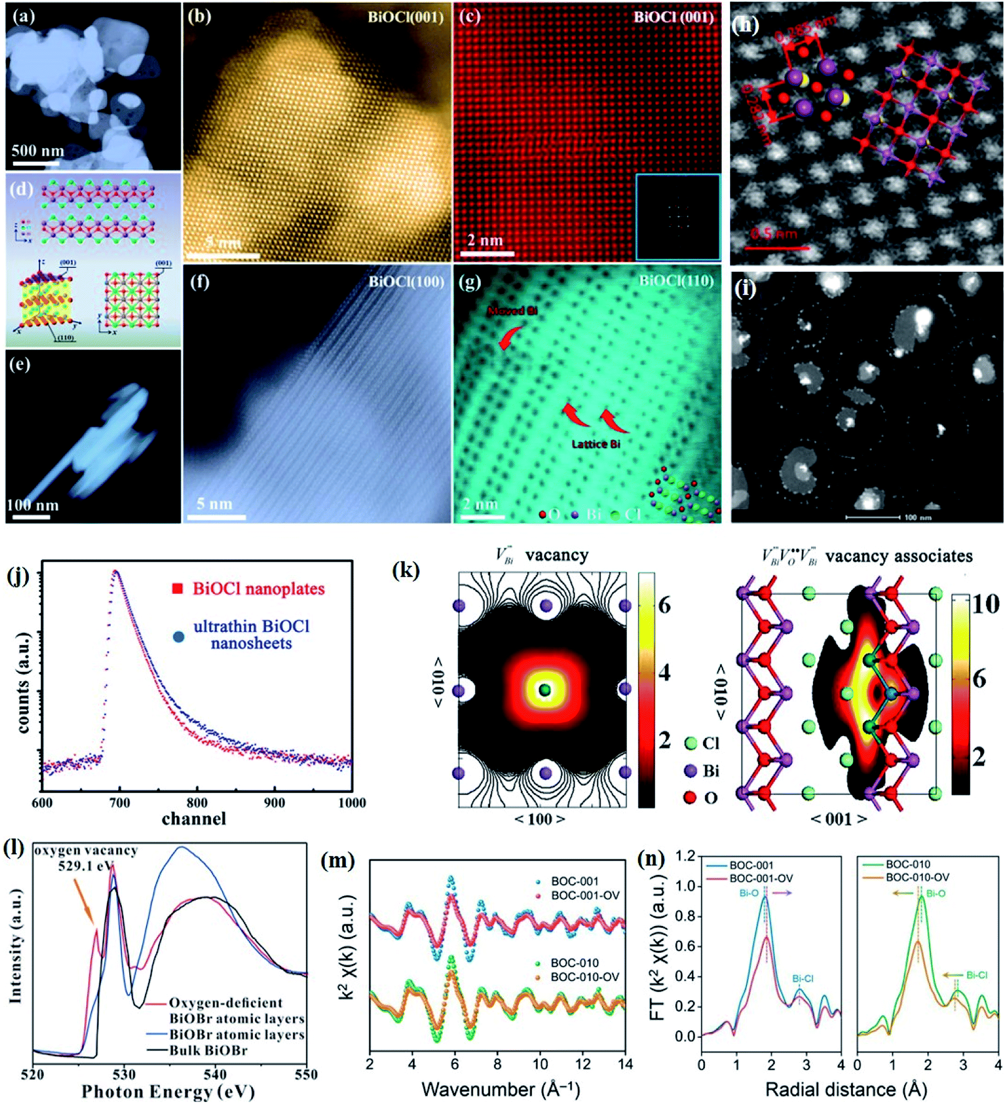 | ||
Fig. 3 HAADF-STEM images of (a) BiOCl (001) facets and the atomic structure images of (b) the outer layer and (c) the grain interior. (d) Schematic diagram of the BiOCl crystal structure. HAADF-STEM images of (e) (100) facets and the atomic structure images of (f) the outer layer and (g) the grain interior.73 Copyright 2018 American Chemical Society. (h) Top view atomic resolution HAADF-STEM image of the Bi2WO6–Bi2O2S nanosheets (the inset shows the crystal structure of the (010) plane of Bi2O2S).89 Copyright 2019 American Chemical Society. (i) HAADF-STEM image (scale bar 100 nm) of the lateral 2D NHS made from Bi2Se3 NSs–CdS NPs.91 Copyright 2015 American Chemical Society. (j) Positron lifetime spectrum of ultrathin BiOCl nanosheets and BiOCl nanoplates, respectively. (k) Schematic representations of trapped positrons of  defect and defect and  vacancy associates, respectively.57 Copyright 2013 American Chemical Society. (l) O K-edge XANES spectra for oxygen-deficient BiOBr atomic layers, BiOBr atomic layers, and bulk BiOBr.96 Copyright 2018 Wiley. (m) Bi L-edge extended XAFS oscillation function k2χ(k) and (n) the corresponding Fourier transforms for BiOCl with and without OVs.97 Copyright 2016 American Chemical Society. vacancy associates, respectively.57 Copyright 2013 American Chemical Society. (l) O K-edge XANES spectra for oxygen-deficient BiOBr atomic layers, BiOBr atomic layers, and bulk BiOBr.96 Copyright 2018 Wiley. (m) Bi L-edge extended XAFS oscillation function k2χ(k) and (n) the corresponding Fourier transforms for BiOCl with and without OVs.97 Copyright 2016 American Chemical Society. | ||
However, the bulk defects cannot be embodied by HAADF-STEM. Positron annihilation, another well-established technique to ascertain the defective structures in solids, can recognize the type and relative concentration of diverse defects/vacancies by measuring the lifetimes of the positron, even at the parts-per-million level.92 For example, Guan et al. employed positron lifetime spectra and corresponding theoretical calculation to identify the defective type of BiOCl nanosheets with different thickness.57 The shortest positron lifetime (τ1) corresponds to the single isolated bismuth vacancies  , while the relatively longer positron lifetime (τ2) is due to the triple vacancy clusters
  (Fig. 3j). Due to the highest relative intensity of τ1 and τ2 for BiOCl nanoplates and BiOCl nanosheets, respectively, the predominant defects are
  instead of
  after the thickness was reduced to the atomic scale (Fig. 3k). Gao and co-workers applied positron annihilation spectroscopy to identify the effect of synthesis temperature on the type and concentration of vacancy in two single-unit-cell BiVO4 nanosheets.92 The shortest positron lifetime validates the presence of vanadium vacancies within two single-unit-cell BiVO4 nanosheets, and a relatively higher positron lifetime indicates that the sample prepared at a higher synthetic temperature has a higher concentration of vanadium vacancies, giving rise to different photocatalytic performance towards CO2 reduction.
Nevertheless, due to the specific structural variations and the lack of long-range order of 2D Bi-based materials, the above-mentioned techniques display significant limitations in characterizing the defined local atomic arrangements involved in ultrathin crystals. By virtue of its deep penetration and extreme sensitivity to the local atomic environment, X-ray absorption spectroscopy is the most commonly employed technique to investigate the structural characteristics at the atomic scale, such as the oxidation state, coordination chemistry, bond length, and atomic species, which has established a series of amazing achievements in the field of photocatalysis.93–95 X-ray absorption spectroscopy includes X-ray absorption near-edge spectroscopy (XANES) and extended X-ray absorption fine-structure spectroscopy (EXAFS). Specifically, XANES is sensitive to the oxidation state and coordination chemistry of the absorbing atom, while EXAFS is used to determine the distances, coordination number, and neighboring species of the absorbing atom. For example, Wu and co-workers verified the impacts of induced VOs in BiOBr atomic layers on photocatalytic processes through XANES technology.96 The O K-edge XANES spectra (Fig. 3l) depict that the extra peak located at 529.1 eV is assigned to VOs resulting from 480 min of UV light irradiation, demonstrating that UV light irradiation leads to the generation of abundant VOs in the BiOBr atomic layers, which is not the case for pristine BiOBr atomic layers and bulk counterparts. Li et al. verified the predicted different atom relaxation behaviors around OVs on the surface of BiOCl-001 and BiOCl-010 by using Bi L-edge EXAFS curves.97 As shown in Fig. 3m, no significant change in frequencies is observed, while an obvious decrease in the amplitude is found after the introduction of surface OVs. The corresponding Fourier transform (FT) of the k2χ(k) functions in R space shows that only a positive shift of the Bi–O peak is detected in BiOCl-001, while a negative shift of both Bi–O and Bi–Cl peaks exists in BiOCl-010, which is in agreement with the DFT predication results (Fig. 3n). Similarly, Dong et al. revealed the coordination numbers and the local atomic arrangements in ultrathin BiVO4 nanosheets via V K-edge EXAFS characterization.98 The BiVO4 nanosheets and their bulk counterpart exhibit similar V K-edge oscillation curves, indicting their same tetrahedral V–O coordination. However, the coordination number of BiVO4 nanosheets is lower than that of the bulk counterpart, suggesting the presence of structural distortion of V cations in BiVO4 nanosheets, which is in line with the generation of abundant VO.
3.2 Electronic structure
The electronic structures directly determine the intrinsic optical and electronic properties of semiconductors, which is associated with the band gap energy, band position and charge carrier behavior, thereby impacting the photoexcitation processes and photocatalytic behaviors involved therein. With this recognition, the investigation on the electronic structure is essential for gaining insight into the photocatalytic mechanism and optimization of the photocatalytic process.In terms of charge carrier dynamics, Kelvin probe force microscopy (KPFM), which is based on the contact potential difference (CPD) between the two contact components, can well reflect the behaviors of charge carriers on the surface and/or at the interface, given by the ultrathin thickness and relatively poor screening effect of 2D materials.99–101 For instance, Zhang et al. disclosed the interplay between Bi2MoO6 and glycol/glycerol/water through KPFM images, as reflected by the change in CPD, denoted as ΔCPD.102 The ΔCPD signal of Bi2MoO6-glycerol is much higher than that of Bi2MoO6-water and Bi2MoO6-glycol, suggesting that more photoinduced holes migrate to the surface driven by the effect of the surface space charge region in Bi2MoO6-glycerol with the smallest thickness. In addition, the surface potential of a photocatalyst can be altered by the interfacial interaction between the 2D materials and is not affected by the thickness of the materials but by the interface structure. In light of this, the detection and control of the potential gradient on the photocatalyst surface are imperative to expose the interface structure and enhance the photocatalytic performance. More importantly, KPFM coupled with irradiation sources enables the direct imaging of photogenerated charge carrier separation within semiconductors. For instance, in situ KPFM is used to image the surface potential change in an ultrathin 2D/2D Bi2WO6–Bi2O2S heterojunction upon light illumination to directly visualize the charge separation behavior at the interface.89 As shown in Fig. 4a and b, both the average potential drop or shift of Bi2WO6–Bi2O2S nanosheets is much higher than that of neat Bi2WO6 nanosheets, indicating a boosted electron buildup on the surface of Bi2WO6–Bi2O2S nanosheets as a result of enhanced charge separation at the interface.
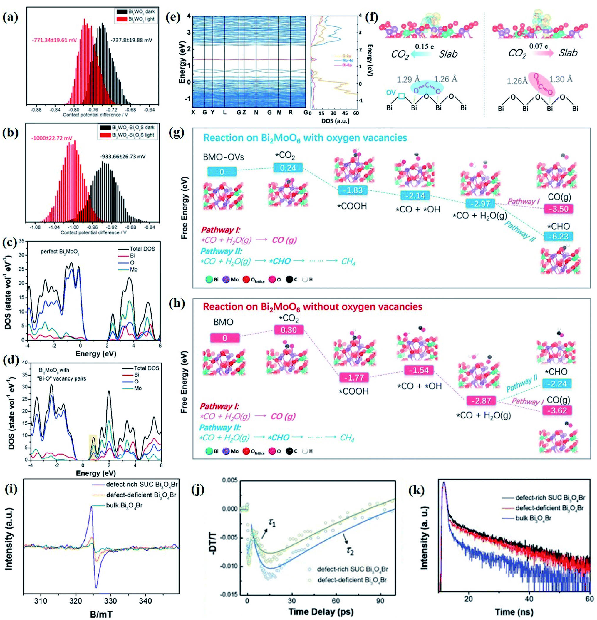 | ||
| Fig. 4 CPD distributions obtained from the sample areas of the KPFM images of (a) monolayered Bi2WO6 and (b) Bi2WO6–Bi2O2S nanosheets.89 Copyright 2019 American Chemical Society. Calculated density of states of (c) perfect Bi2MoO6 and (d) Bi2MoO6 with “Bi–O” vacancy pairs.109 Copyright 2019 Elsevier. (e) Calculated band structures and total DOS of Bi2MoO6-OVs. (f) Absorption of B1-CO2 on Bi2MoO6-OVs and B2-CO2 on Bi2MoO6. Reaction pathways for CO2 reduction on (g) Bi2MoO6-OVs and (h) Bi2MoO6.110 Copyright 2019 Elsevier. (i) Low-temperature EPR of defect-rich and defect-deficient Bi3O4Br. (j) Ultrafast TA spectrum (400 nm pump and probed at 532 nm). (k) Time-resolved transient PL decay.90 Copyright 2019 Wiley. | ||
Moreover, first-principles calculations, especially DFT calculations, are a powerful and intuitive tool to gain insights into the geometric structure and optical and electronic properties of photocatalysts.103 In terms of 2D materials' design, DFT calculations can provide reliable prediction and guidance prior to synthesis under experimental conditions with the development of condensed matter sciences.104,105 At present, many new 2D materials with diverse compositions and structural characteristics are constantly being predicted through accurate structure search techniques based on DFT calculations. Although topological modelling methods can effectively predict new 2D structures via evaluating the energy of a large number of enumerated structures, it is quite cumbersome and limited to small supercell.106 In this regard, a cluster expansion approach that parametrizes the energy of structures as a polynomial in the occupation variables is developed, and can quickly converge and immediately calculate the energy of any configuration.
It is worth noting that the structure prediction is not the end of material design, considering that special electronic and optical properties are required for photocatalytic applications. These properties including the bandgap width, band edge position, optical adsorption, and charge carrier mobility can be accurately calculated by DFT simulations. For instance, Fu et al. applied plane wave DFT calculations to predict the electronic structure of Bi2WO6, and found that the VB of Bi2WO6 is composed of O 2p and Bi 6s hybrid orbitals, while the CB consists of W 5d orbitals, with the band gap determined to be 1.63 eV.107 The relatively narrow band gap allows Bi2WO6 to be excited under visible light irradiation to generate photogenerated charge carriers, and the hybridization of Bi 6s and O 2p makes the VB more dispersed which contributes to high hole mobility. Thanks to the above properties, nanosized Bi2WO6 photocatalysts exhibit outstanding potential in environmental purification and energy conversion.
Nevertheless, the overall photocatalytic performance of single semiconductors is still relatively poor due to fast recombination of photogenerated electron–hole pairs, a limited light absorption region, and weak redox ability. To overcome this problem, various strategies such as heteroatom doping, inducing defects, etc. are developed to optimize the structure and activity of a single semiconduction. Such structural changes related to order–disorder can only be reflected by DFT simulations. As reported by Di et al., based on DFT calculations, it is found that the VBi–BiOBr sample displays a downshifted VB edge with a leveled up CB potential as compared to perfect BiOBr, indicative of a higher charge density near the Fermi level caused by the introduction of Bi vacancies.108 The diverse local atomic structures of VBi–BiOBr and BiOBr result in distinct electronic structures, which further lead to different photocatalytic mechanisms, that is, a large number of 1O2 molecules are generated in the VBi–BiOBr system but are almost negligible in the BiOBr nanosheets. Their group further confirms that the change in the electronic structure of the Bi2MoO6 ultrathin nanosheets is attributed to the “Bi–O” vacancy pairs through DFT calculation, as demonstrated by the increased DOS at the VB edge and newly generated DOS in the forbidden band of defective Bi2MoO6 (Fig. 4c and d).109
Aside from that, DFT simulation is also effective in predicting possible photocatalytic pathways or charge carrier behaviors prior to specific experiments, which not only guides material synthesis, but also facilitates the optimization of photocatalytic processes. For instance, in comparison with perfect Bi2MoO6, a new intermediate band made up of Bi 6p is detected between the CB and VB in OV-decorated Bi2MoO6 (Bi2MoO6-OVs) (Fig. 4e), implying that the generated defect level might promote the electron excitation and charge separation.110 Comparing the CO2 adsorption energies on two different Bi2MoO6 models, it can be predicted that the bending mode rather than the linear mode is more in line with the CO2 adsorption modes on the surface of both perfect Bi2MoO6 and Bi2MoO6-OVs. However, the two self-O atoms of CO2 molecules are prone to bound with two surface Bi centers in Bi2MoO6-OVs with ΔEabs = −0.47 eV, while only one self-O atom of CO2 molecules is bound to the surface single Bi atom, with ΔEabs = −0.39 eV (Fig. 4f). Such different CO2 adsorption modes ultimately result in distinct CO2 activation levels and selective reduction products (Fig. 4g and h). Likewise, Li et al. employed theoretical calculation to predict the possible mechanism of N2 activation on the OVs of (001) facets of BiOBr.111 The N2 adsorption model is predicted to be an end-on bound structure according to the change of Bader charge of the two OV connected Bi atoms, and it can be conjectured that the N2 activation pathway follows the electron back-donation principle based on the difference in charge density.
More importantly, aside from the significant merit of 2D materials, excitons related to the optical and electronic properties of semiconductors should also be considered due to the decreased size in the third dimension, especially the competition between exciton and charge carriers. Toward this end, the kinetic evaluation of the photocatalytic process involving excitons should not be solely the role of carriers. In analogy to carrier-involved photocatalytic reactions, exciton-involved reactions can also be predicted by simulating the CB and VB band-edge states. For instance, the band edges of BiOX (X = Cl, Br, I) are estimated to be much higher than that of most inorganic semiconductors according to DFT calculation, which implies the presence of strong excitonic effects within BiOX semiconductors.112 In conjunction with the results of the influence of halogen elements on the excitonic effects in BiOX, they conjectured that the formation of excitons in confined [Bi2O2] slabs is due to the interaction between photogenerated electrons and holes, and thus the internal electric field plays a negligible role in charge separation. In order to verify the above predications, the molecular oxygen activation behavior on the (001) and (010) facets of BiOBr is evaluated, and the 1O2 yield on the (001) facet is much higher than that on the (010) facets, coinciding with expectations.
From above, DFT simulation is demonstrated to be a powerful and fundamental tool to reveal the intrinsic information of a photocatalyst, with the accuracy ranging from atoms, molecules to unit cells.113 However, as the composition of the photocatalytic reaction system becomes more complex, the limitations of DFT calculation in revealing the photocatalytic mechanism are gradually exposed. To start with, DFT calculation can only reflect the ground state information of the system, and the theoretical simulation can qualitatively predict the behavioral trends of photobiological species including charge carriers and excitons, but cannot provide detailed kinetic analysis. Next, DFT simulations can effectively predict the structure of single-component photocatalysts, but fail to predict 2D heterojunction structures. What's more, as for a composite system, the properties of the selected surface and surface-exposed atoms will greatly influence the lattice matching and interface interaction, but there is still no general standard for this selection. Besides, the real scene of a specific photocatalytic reaction, covering light irradiation and the generation and transfer of charge carriers, cannot be directly simulated. Last but not least, although many 2D material models have been proposed based on DFT calculation, there is little room for exploring eye-catching 2D photocatalysts in practical applications, which is limited to a restricted group of a few possible ones due to high-throughput material screening. The direct adverse result is that those selected materials may display detrimental characteristics, of which the thermodynamic stability related to the materials' properties is a prerequisite in the screening process of 2D material candidates.
Currently, the structural stability of materials is evaluated via DFT formation energy calculation, which results in high costs for exhausting each possible material. In light of this, further research is devoted to determining a set of stable structures for a given atomic combination with a specific stoichiometric ratio, so as to screen out the most stable structures a priori. Fortunately, based on simulation calculations, several advanced methodologies have been developed to predict the stability of 2D material systems, such as a topology-scaling algorithm,114 DFT lattice constant difference,115 creating a computational 2D material database.116 Nevertheless, the exploration of 2D materials is mainly focused on compounds with van der Waals forces, which greatly limits the development space of 2D materials compared with numerous 3D materials. To overcome this obstacle, on the basis of calculating the total energies and convex hull energies, Gabriel et al. employed machine learning techniques to define a global property of 2D materials with thermodynamic stability rather than using a different regression model for each of these properties.117 This method can well identify the stable structures and classify 2D materials as having low, medium, or high stability, which facilitates to evaluate the stability of novel 2D materials for further detailed investigation of promising candidates, showing great potential for specific applications.
3.3 Photoexcitation process investigation
As for the principle of photocatalysis, the initial step of the photocatalytic reaction is a photoexcitation process after the material harvests energy above its band gap. Commonly, energy band theory can well explain the charge-carrier-involved photocatalytic process, whereas the excitonic effects in low-dimensional materials will establish distinct photocatalytic mechanisms outside of conventional, which cannot be accurately descripted via band theory. In this regard, insight into the photoexcitation process is highly desirable in determining the photocatalytic mechanism.Excitons or electron–hole pairs bound by attractive Coulomb interactions are competitors to charge carriers in the photoexcitation process, and the excitonic effect directly affects the dynamic mechanism of a charge-carrier-involved photocatalytic system. In general, the excitonic effect is relatively weak in 2D non-layered Bi-based materials, which is because a large number of unsaturated bonds present on the surface enrich the surface with traps, thus resulting in strong non-radiative decay or rapid exciton dissociation.118 However, the excitonic effect is significantly obvious in layer-structured materials due to reduced electronic screening effects and increased structural confinement, which will interfere with the photoexcitation process. To be specific, the competitive relationship between excitons and carriers in a photoexcitation process will result in a decrease in carrier yields, and excitons are easily annihilated with other excitons at high concentrations, leading to a reduction in light-induced species, both of which are not conducive to an encouraging improvement in photocatalytic performance. However, recent work proposed that exciton conversion between singlet and triplet states is beneficial for the generation of 1O2, which can advance the photocatalytic process.119 In addition, promoting the dissociation of excitons into free electrons and holes can not only overcome the adverse excitonic effects on the charge-carrier-involved photocatalytic process, but can even play a positive role. For this reason, only by understanding the excitonic effects can we accurately evaluate the photoexcitation process of 2D Bi-based materials, which can be achieved by monitoring the behavior of photoinduced species including excitons and charge carriers in the photoexcitation process.
Photoluminescence spectroscopy as a result of radiative decay of photoinduced species has been regarded as an effective technology to detect the relaxation paths and kinetics of photoinduced species. For example, Liu et al. illustrated the positive role of interfacial VOs in Bi2O2CO3/graphene quantum dot composites (N-BOC/GQDs) for photocatalytic NO oxidation by photoluminescence spectroscopy.83 The steady-state photoluminescence spectra show an obvious decrease in the photoluminescence intensity after modifying N-BOC with GQDs, indicative of upgraded charge separation efficiency within N-BOC/GQDs. Further time-resolved photoluminescence measurements under different light irradiation corroborates that the synchronized emissive state depopulation in N-BOC/GQDs under UV light is due to the Z-scheme recombination mechanism between the VB-holes of GQDs and the electrons at the defect states of N-BOC. In addition to interfacial VOs, Li et al. revealed the positive effect of surface VOs in BiOBr on photocatalytic N2 fixation using photoluminescence measurements.111 The significantly decreased photoluminescence intensity under a N2 atmosphere indicates that surface VOs as an electron acceptor are responsible for the electron transfer from BiOBr to the adsorbed N2, thereby ameliorating the adsorption and activation efficiency of N2 on the defect. Moreover, given that the engineered surface metal vacancies will give rise to conspicuous electronic structure variation relative to perfect ones, arising from the diversified electron configuration and orbit of metal cations, Di and his group verified the effect of Bi vacancies on the photocatalytic performance of BiOBr ultrathin nanosheets.108 Time-resolved fluorescence emission decay spectra showed that VBi–BiOBr UNs display a greatly longer average lifetime than that of perfect BiOBr nanosheets, which is attribute to the surface Bi vacancies as separation centers. Therefore, more photogenerated electrons can reach the surface and activate the adsorbed CO2 molecules to trigger the conversion process.
As demonstrated above, photoluminescence measurements present unparalleled advantages in determining the behavior of photoinduced species in a photoexcitation process. Nonetheless, due to the femtosecond-level, nonradiative relaxation processes and the complicated profiles of the light/dark state of the photoinduced species, establishing a comprehensive understanding on the photoexcitation processes is still the bottleneck of current research. Fortunately, with the rapid development of lasers with ultra-high resolution and power, ultrafast transient absorption (TA) measurements have enabled the monitoring of ultrafast photoexcitation processes, and thus, gained deep insights into the photocatalytic process. More importantly, TA technology can realize the real-time tracking of the relaxation kinetics of photogenerated charge carriers in semiconductor systems.120 For instance, Di et al. revealed the effect of surface defect concentration on the separation, transfer, and recombination process of photogenerated charge carriers in Bi3O4Br through femtosecond resolved TA spectroscopy.90 As is well known, the τ2 value reflects the charge separation process induced by defects, as the τ2 value of defect-rich Bi3O4Br (120 ps) is smaller than that of defect-deficient Bi3O4Br (140 ps), which suggests a faster charge separation rate in defect-rich Bi3O4Br (Fig. 4i and j). In other words, the more defect states in the band gap, the better the rapid capture of electrons. At the same time, the photoluminescence decay curves show that defect-rich Bi3O4Br has a longer lifetime than bulk and defect-deficient Bi3O4Br (Fig. 4k), indicating the positive role of surface defects in charge separation, which agrees well with the TA characterization. Also, Wang et al. revealed the distinct excitonic processes between BiOBr(001) and BiOBr(010), as reflected by the pronounced difference in the TA kinetic trace.112 That is, both BiOBr(001) and BiOBr(010) exhibit photo-absorption profiles, while BiOBr(001) displays pronounced pump-fluence-dependent TA kinetics but a faint dependence within BiOBr(010).
In fact, it is commonplace now that photocatalysts are dynamic systems that change as the reaction proceeds, rather than just a static arrangement of atoms. Hence, it is rather difficult for conventional characterization techniques to monitor the transient evolutions of reaction intermediates under realistic reaction conditions. Moreover, the real-time detection of the reaction intermediates and the final products is favorable for accurately revealing the reaction mechanism, which can provide reliable guidance for further improving the performance of photocatalysts.121 In this regard, developing in situ characterization techniques to reflect the dynamic evolution of photocatalysts and detect the intermediate of the photocatalytic system in real time is highly desired.
Currently, a series of in situ characterization techniques are employed to monitor a dynamic process in real time, where in situ FTIR spectroscopy based on detecting the evolution of surface chemical groups is widely used to speculate the reaction intermediates. For instance, Huang and co-worker employed in situ FTIR spectroscopy to detect the functional groups generated on the surface of a Bi2Se3/g-C3N4 composite in the photocatalytic process.122 Several obvious peaks are observed with light on, and their peak intensity strengthens with increasing irradiation time. The peaks located at 1210–1250 cm−1 and 1613–1770 cm−1 are assigned to COOH* groups, bidentate bicarbonate species (b-HCO3−), monodentate carbonate (m-CO32−), bidentate carbonate (b-CO32−), and bent carboxylate (CO2−), and those peaks disappear with the light off, suggesting that all of them are the intermediates of photocatalytic CO2 reduction. Based on the above in situ FTIR analysis, it can be deduced that adsorbed CO2 is firstly activated under light irradiation to form CO2* species, followed by reacting with the surface protons to generate COOH* and then CO* species, with CO as the final product. Therefore, in situ FTIR spectroscopy is widely recognized as a powerful tool for real-time monitoring the dynamic changes of reaction intermediates, which provides reliable information for inferring the reaction pathways and mechanisms. In another example, in situ water contact angle measurements are used to evaluate the effect of defects on the interaction between water and the photocatalyst surface (Fig. 5a).97 As displayed in Fig. 5b, it is found that the water contact angle gradually decreases with the increase of UV light irradiation for both BOC-001 and BOC-010 while no obvious change can be detected over time in the dark, indicating that the photoinduced hydrophilic conversion is due to the introduction of defects under UV irradiation. Besides, the water contact angle on the BOC-010 surface is much smaller than that on BOC-001 before and after UV light illumination for 120 min, suggesting that the water–surface interaction on BOC-010 is much stronger than that on BOC-001, giving rise to a higher water activation level.
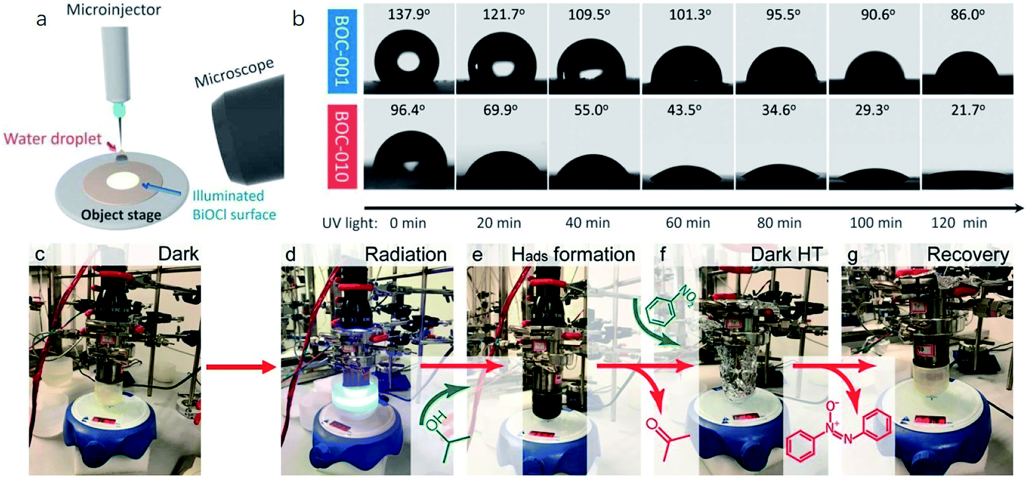 | ||
| Fig. 5 In situ water contact angle measurements on the BiOCl surfaces. (a) Schematic presentation of water contact angle measurement. A UV light source was set above the BiOCl cylindrical pellets, and the water contact angle was monitored in situ via a microscope connected to a computer. (b) Photos of the water droplets on the BiOCl surfaces under UV light illumination.97 Copyright 2016 American Chemical Society. (c–g) Photographs of the stepwise hydrogen transfer process: fresh Bi24O31Br10(OH)δ–isopropanol suspension without irradiation, under irradiation (450 nm), hydrogenated catalyst (black suspension) with the generation of acetone, nitrobenzene addition, nitrobenzene reduction by Habs under dark conditions, and recovery of the photocatalyst.123 Copyright 2018 American Chemical Society. | ||
Moreover, the real-time detection of photocatalytic products is equally important for a specific reaction, especially for evaluating the relationship between reaction conditions and the distribution of photocatalytic products. For example, in order to reveal the contribution of surface basic sites to the stepwise hydrogen transfer process over a Bi24O31Br10(OH)δ photocatalyst, a control experiment is conducted (Fig. 5c–g).123 The pale-yellow suspension of photocatalyst-isopropanol gradually turns black with blue light on, and gas chromatography-mass spectrometry (GC-MS) analysis demonstrates the generation of acetone, indicating that the Bi24O31Br10(OH)δ photocatalyst is hydrogenated by the surface-adsorbed H (Hads). After dosing nitrobenzene into the above suspension in the dark, the pale-yellow color is gradually recovered, which indicates that some or all Hads is consumed, confirming that irradiation is not essential for the consecutive hydrogen transfer step once Hads atoms are formed. More importantly, further in situ mass spectrometry analysis showed that neither H2 nor O2 is generated, demonstrating that the unconsumed Hads combines with oxygen atoms in nitrobenzene to form water. Aside from above, some other advanced in situ characterization techniques are also widely applied to the real-time monitor of photocatalyst evolution. In situ XRD and in situ X-ray absorption fine structure (XAFS) measurements are used to reflect the phase transformation of photocatalysts, the in situ XPS technique is applied to characterize the valence state changes, in situ TEM can real-time detect the morphology evolutions of the photocatalyst, in situ XAS is an ideal technique to monitor the local coordination environment of samples in the reaction process, and so on.124 However, it should be noted that each in situ characterization technique can only real-time monitor the evolution of a certain aspect of the photocatalyst in the reaction process, and thus technical combination is highly desired for in situ studies. Moreover, apart from experimental evidence, a theoretical model is also established to simulate the catalytic reaction with the development of theoretical techniques and advanced algorithms, which provides an in-depth insight into the reaction process at the atomic level. In light of this, combining in situ characterization techniques and theoretical calculations is favorable for deeply probing the reaction mechanism, which provides more detailed information for optimizing the structure and performance of photocatalysts.
4. Engineering protocols for catalyst design
As mentioned in Section 2, there are various parameters associated with the surface and interface properties, such as facets, defects, pore structure, atom structure, and so on. Accordingly, preparing a high-performance 2D Bi-based photocatalyst with favorable surface and interface properties is extremely important for its practical application. In this section, various engineering protocols based on surface and interface parameter optimization in a 2D Bi-based photocatalytic system will be summarized, with the aim to give rise to an ameliorated photocatalytic performance.4.1 Surface engineering
 | ||
| Fig. 6 (a) The scheme of enhanced charge transfer in bulk BiMoO6 and ultrathin C-BiMoO6.126 Copyright 2017 Wiley. (b) Bulk charge separation efficiency (ηbulk) and variation in the internal electric field intensity of C-doped Bi3O4Cl (the inset is the result of assuming that the BOC IEF intensity is “1”). (c) Visible-light photocatalytic oxygen evolution of carbon-doped Bi3O4Cl (Bi3O4Cl doped with 0.92%, 1.86%, and 3.16% carbon concentration, denoted as BOC-C1, BOC-C2, and BOC-C3, respectively).127 Copyright 2016 Wiley. Calculated band structures of (d) Bi2WO6 and (e) Bi2+xWO6. Total density of states of (f) Bi2WO6 and (g) Bi2+xWO6.132 Copyright 2014 American Chemical Society. | ||
Outside of generating doping levels in the band gap structure, the heteroatoms exist in the form of substitutional dopants at the edges or in the basal plane of 2D materials, which will inevitably disrupt the host atom network, leading to the generation of defects that can function as extra active sites to trigger surface reactions.128 For instance, Wang et al. reported that Co doping results in the generation of new defect levels above the Fermi level of BiVO4, and at the same time, Co atoms in the BiVO4 atomic layers serve as active centers for water oxidation.129 In comparison with pure BiVO4 with the top of the VB composed of O 2p orbits, the top of the VB for Co-doped BiVO4 is mainly occupied by Co 3d orbits, and thus the Co atoms provide active sites for excited holes to participate in the surface oxygen evolution reaction. Likewise, Lei et al. reported that Fe(III) doping can introduce unique active sites on the surface of BiOCl ultrathin nanosheets, which facilitates the surface reaction.130
Given that heteroatom doping may result in thermal instability of materials due to the introduction of foreign impurities, the self-doping strategy can well avoid the negative impact of foreign element doping, and can also tune the electronic structures. Inspired by this, Zhang's group reported that the CB bottom of BiOI is depressed and the Bi 6s orbit composition is increased after I 5p orbits were incorporated with iodine dopants as compared to the undoped sample.131 The narrowed band gap promotes the optical absorption region, and the charge separation efficiency is also improved, contributing to the dispersive characteristic of the s orbital, and taking advantage of this, the doped sample exhibits superior photocatalytic performance. Beyond non-metal self-doping, their group further dedicates to metal self-doping, taking the substitution of W in Bi2WO6 by Bi as a model (Fig. 6d and e).132 Computations based on DFT show that the Bader charges of oxygen atoms around the substituted Bi atom are attenuated slightly compared with the undoped sample, indicating the charge redistribution around the dopant of Bi2+xWO6. Moreover, apart from the CB and VB, a new band below CB position, which is composed of an O 2p orbital, is detected in the Bi self-doping sample, which promotes electron excitation within Bi2+xWO6 (Fig. 6f and g). Therefore, Bi2+xWO6 nanosheets can generate more superoxide ions due to the strengthened internal electric field and increased carrier density.
At the atomic level, atomic vacancies can be inherently present or introduced, representing the widely investigated type of defect in heterogeneous photocatalysis. In general, the surface vacancies usually function as the donor and/or acceptor center for certain photoinduced species, which, in turn, promotes the separation of charge carriers. For instance, by fitting the transient photoresponse, Wang et al. unearthed that BiOCl and BiOCl-OVs have the same relaxation time of 0.3 s in the fast decay process, suggesting no difference in the photoinduced electron–hole recombination process between the two samples.134 However, in the slow decay process, the relaxation time of BiOCl-OVs is much higher than that of perfect BiOCl, which indicates a larger local potential fluctuation in BiOCl-OVs, showing that VOs can capture the excited electrons to accelerate the dissociation of photogenerated charge carriers (Fig. 7a and b). Meanwhile, the introduction of VOs can also optimize the light absorption capacity of the sample, as evidenced by an additional decaying absorption tail extended to 600 nm in the UV-vis spectrum of BiOCl-OVs. Moreover, given the special geometric features of 2D materials, surface atoms are more likely to escape from the surface lattice as the size of the third-dimension decreases, which will cause the type of surface defect to change accordingly, as confirmed by Li and co-worker.135 After the thickness of BiO2−x was reduced from nanoplates to a monolayer, the dominant vacancy type changes from single VOs to dual vacancies  (Fig. 7c and d). The monolayer thickness results in partial Bi atoms exposed outside, which much more easily escape from the lattice, leading to the formation of dual vacancies. Therefore, the
  vacancy present in the band gap of BiO2−x monolayers can even capture the low photonic energy, resulting in a higher photocatalytic performance for BiO2−x monolayers in a wide light region from UV to near-infrared light.
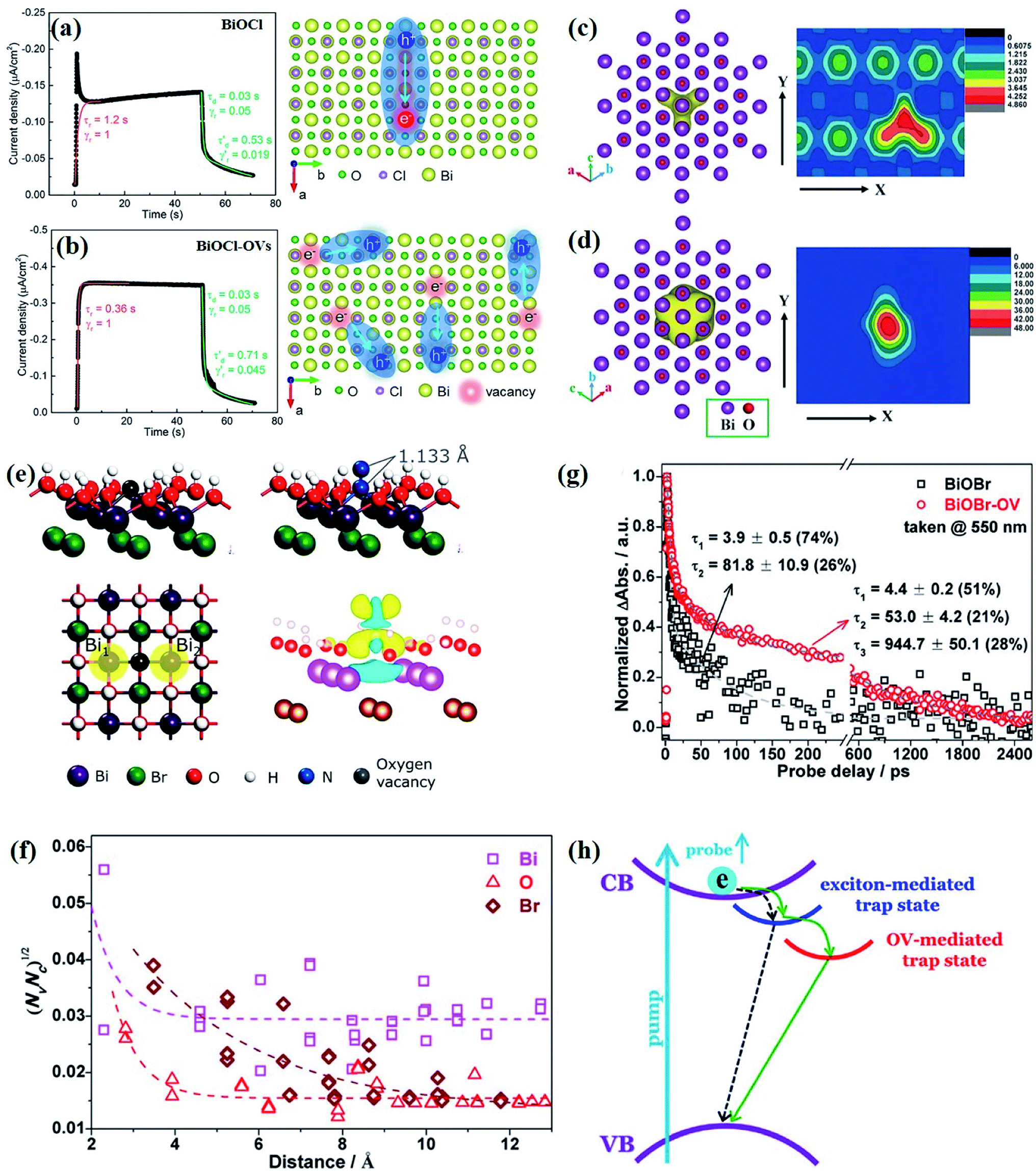 | ||
Fig. 7 Acquired rise and decay times of (a) BiOCl and (b) BiOCl-OVs by fitting the on/off curve and corresponding crystal structure with the proposed photoexcited charge carriers.134 Copyright 2019 American Chemical Society. Positron density distribution (yellow) in BiO2−x with (c)  defects and (d) defects and (d)  defects, respectively.135 Copyright 2018 Wiley. (e) Theoretical prediction of N2 adsorption and activation on the OV of the BiOBr (001) surface.111 Copyright 2015 American Chemical Society. (f) (NcNv)1/2 value of atomic sites at different distances around the oxygen vacancy. (g) TA kinetic traces probed at 550 nm for both samples. (h) Schematic illustration of the photophysical processes involving exciton- and oxygen-vacancy-mediated trap states.136 Copyright 2018 American Chemical Society. defects, respectively.135 Copyright 2018 Wiley. (e) Theoretical prediction of N2 adsorption and activation on the OV of the BiOBr (001) surface.111 Copyright 2015 American Chemical Society. (f) (NcNv)1/2 value of atomic sites at different distances around the oxygen vacancy. (g) TA kinetic traces probed at 550 nm for both samples. (h) Schematic illustration of the photophysical processes involving exciton- and oxygen-vacancy-mediated trap states.136 Copyright 2018 American Chemical Society. | ||
In addition to the aforementioned positive effects of defects on expanding the light absorption region and promoting the charge transfer separation within a semiconductor, unremitting efforts have been devoted to investigating the role of defects in various chemical reactions. For instance, OVs can provide a Lewis-base for electron accumulation and unsaturated–unsaturated sites for catalytic reactivity, which guides chemical reactions to overcome the obstacles that require high thermodynamic activation energy on the ideal crystal surface to excite the reaction. As for surface photocatalytic reactions, adsorption and activation processes often take place on the coordinately unsaturated sites that are thermodynamically instable. The dangling bonds in the sites are prone to capture both charge carriers and reactants, and thus the types and numbers of surface defects or vacancies will affect photocatalytic activity and selectivity. With OV-rich BiOBr nanosheets exposed by (001) facets as an example, Li et al. theoretically revealed that the OVs with abundant localized electrons can promote the adsorption of N2 molecules, and act as a charge carrier acceptor to facilitate the separation of photogenerated electron–hole pairs.111 More importantly, the surface OVs can effectively activate the adsorbed N2via N–N triple bond, as demonstrated by the increase of the N–N bond length up to 1.133 Å (Fig. 7e). This activation behavior is due to the presence of Lewis-base and unsaturated–unsaturated sites on the OVs of BiOBr, which leads to the transfer of excited electrons from the CB of BiOBr to the adsorbed N2, and thus achieves higher N2 reduction efficiency in OV-rich BiOBr compared with perfect BiOBr nanosheets.
As previously discussed, the exciton effect of 2D materials should be considered when evaluating the photocatalytic activity involving photogenerated charge carriers. Since the distribution of electronic states within the photocatalyst is greatly distorted when defects are introduced, gaining insight into its effects on the exciton dissociation is helpful to accurately reveal the photocatalytic carrier dynamics of semiconductors. Taken BiOBr as an example, by calculating the numbers of localized valence and conduction states near band edges for different atoms, it is expected to find the extended band-edge states around the vacancy site, indicating that the excitons will become less compact and unstable (Fig. 7f).136 That is to say, the photo-induced excitons will relax to the VO-mediated trap state and meanwhile be dissociated into free charge carriers around the VOs within defective BiOBr, which can be verified by fitting the TA kinetics to a triexponential decay function in BiOBr-OV with a biexponential decay function in perfect BiOBr (Fig. 7g and h). As a result, the activation of O2 in defective BiOBr is achieved by electron delivery, with ˙O2− as the dominant active species, while in the case of perfect BiOBr, the activation of O2 is driven by the photo-induced excitonic effects, activating O2 into 1O2via energy transfer. Therefore, as for photocatalytic reactions involving excitonic effects, the effect of defects on the exciton dissociation should be taken into consideration, which provides a chance to manipulate O2 activation.
Additionally, vacancies can induce the chemical coordination of different atoms, which provides unprecedented opportunities to integrate individuals into composite nanostructures, and the generated interface is more stable compared with those formed by electrostatic force, van der Waals force, etc. The work by Li and co-worker reported that MoS2 monolayers can be selectively assembled onto [Bi12O17−x] end-faces with the assistance of chemical reactivity of OVs.137 Specifically, OVs can mediate the chemical coordination of unsaturated Bi atoms near the OV sites with the S atoms terminated on the MoS2 surface to form Bi–S bonds. The Bi–S bonds can function as highways for the interfacial electron transfer from [Bi12O17−x] end-faces to MoS2 monolayers, achieving an efficient charge separation at the atomic level, which gives rise to improved photocatalytic performance for hydrogen evolution over Bi12O17Cl2/MoS2 composites.
Taken together, several crucial functions of defect engineering contributing to boosted photocatalytic performance can be concluded as follows. To begin with, they may diametrically participate in the photocatalytic reaction by building intensive interplay between target molecules and defect sites, thereby breaking the bond and decomposing the molecule. Moreover, introducing favorable defects can regulate the electronic structure of the photocatalyst, resulting in an optimized light absorption ability, carrier concentration and electrical conductivity, so as to improve the overall photocatalytic performance. Afterwards, the defect-mediated trapping state can capture photogenerated electrons, enabling more long-lived, trapped electrons to participate in surface reactions. Eventually, part of the defect sites are conducive to the adsorption and activation of specific small molecules, facilitating the photocatalytic conversion process.
Generally, the reactive sites on the surface of the catalyst are mainly determined by the surface state, and thus state regulation can optimize the characteristics of light absorption, charge transfer and separation of the semiconductor. For example, Zhou and co-workers demonstrated the pivotal role of Br− ions in the fabrication of Bi2WO6 monolayers with the assistance of CTAB.138 Theoretical simulations show that the adsorbed Br− ions on the highly exposed, coordinatively unsaturated Bi atoms significantly affect the electronic structure of Bi2WO6 monolayers, suggesting the dominant contribution of the hybridized orbital of Bi 6s, O 2p and Br 4p to the VB (Fig. 8a), giving rise to a narrower band gap (Fig. 8b), as compared to the unmodified monolayers and the nanocrystals. Interestingly, based on DFT calculation, Wang et al. reported that the introduction of Br− promotes the generation of OVs on the (001) facets of Bi2MoO6, while hardly affecting that on (010) facets, which is due to lower energy barriers for the generation of an intermediate state of OVs on (001) facets (Fig. 8c).139 Meanwhile, compared with Bi-OVs and Mo-OVs, the barrier energy of Bi-OVs-Br and Mo-OVs-Br is greatly reduced, indicating that Br− can stabilize the OVs on the (001) facets of Bi2MoO6. Due to those boosted and stabilized OVs, Bi2MoO6-001 samples exhibit improved photocatalytic activity and selectivity towards NO removal (Fig. 8d).
 | ||
| Fig. 8 (a) Calculated DOS of bulk Bi2WO6, the pristine monolayer and the Br-modified monolayer. The Fermi level is taken as the energy zero. (b) Band energy diagrams of Bi2WO6 nanocrystals and monolayers.138 Copyright 2015 Nature Publishing Group. (c) EPR spectra of BMO-001, BMO-001-Br, BMO-010 and BMO-010-Br. Copyright 2020 Elsevier. (d) The reactant steps of Bi-OV formation on (001) facets and (010) facets, respectively.139 Copyright 2020 Elsevier. | ||
Furthermore, owing to the difference in the surface state, surface functionalization will result in surface atom reformation due to the chemical bonding between surface terminal atoms and functional groups, which imparts unexpected photocatalytic performance. For instance, compared to BiOI prepared with H2O as the solvent, the surface atom ratios of Bi to I in BiOI obtained with glycerol exhibit an obvious increase from 1:1.02 to 1:0.97, which is attributed to the chemical bond binding between lone pair electrons in I ions and empty orbitals in O atoms of hydroxyls.140 Such selective chemisorption makes I atoms prone to expose on the surface, integrated with the surface structure reconstruction, resulting in a positive shift of the VB maximum from 1.32 eV to 1.50 eV. As a consequent, the surface bonded hydroxyl can serve as the binding site for free hydroxyl groups in the system, which, in turn, increases the production rate and yield of active oxygen species. Moreover, Wu and co-workers proposed that the formation mechanism of photoinduced OVs in BiOCl is due to the surficial hydroxyl groups.141 Theoretical calculations indicate that the introduction of the hydroxyl group leads to an increase in the bond length of Bi–O and a decrease in its bonding energy, which makes the Bi–O bond easily broken under high-energy UV light irradiation to generate OVs. The formed OVs are energetically beneficial for the dissociation of H2O into hydroxyl groups via proton transfer from H2O to a neighboring bridging O atom, leading to the regeneration of the BiOCl photocatalyst. Aside from these findings, Dai et al. reported that the detrimental factor of low quantum efficiency of Bi24O31Br10 towards hydrogen transfer can be overcome by surface basic site decoration.123 The basic sites with low-coordinated OH and O atoms can initiate the surface alcohol oxidation to get protons, followed by accepting the CB electrons to generate adsorbed hydrogen, which can be efficiently trapped by hydrogen acceptors instead of being released as H2 gas. More surprisingly, Weng et al. reported that the photocatalytic degradation of 2-naphthol over BiOCl nanosheets under visible light irradiation is due to the surface complex between the Bi atom at the surface terminal of BiOCl and the carbon atom of 2-naphthol, with the formation of a Bi–O–C10H7 complex on the surface of BiOCl.142 This surface complex induces a novel charge-transfer-complex pathway that is different from the reported photosensitization or excitonic effect, that is, the excited electrons generated by the Bi–O–C10H7 complex are transferred to the CB of BiOCl, which confers excellent visible light response performance to BiOCl.
As the first step of the catalytic reaction is the adsorption of reactant molecules, the variation in the adsorption of different facets might drive different reaction routes. For instance, BiOCl nanosheets with different facet exposure, (001) and (010) facets, were prepared, and was applied to investigate the facet-dependent photocatalytic performance.42 With MO as a model pollutant, it is found that the adsorption capacity towards MO of BiOCl-001 is much higher than that of the BiOCl-010 sample, as the (001) facets with oxygen atoms as terminations are more negatively charged. This difference results in two distinct facet-dependent mechanisms for photocatalytic dye degradation, that is, direct degradation by the photoexcited charge carriers under UV light and indirect degradation through dye photosensitization under visible light are feasible in (001) and (010) facet-exposed samples, respectively (Fig. 9a and b). Aside from pollutant adsorption, the facet-dependent adsorption behavior is also reflected in the generation of radicals. With OV-rich BiOCl nanosheets as an example, distinct molecular oxygen activation behavior is found on the OV sites of (001) and (010) facets, due to the different surface atomic structure of these two facets (Fig. 9c–g).66 As shown in Fig. 9h, molecular oxygen combines with the two nearest sublayer Bi atoms near the OV sites through end-on bridging on (001) facets, followed by extracting one electron from redistributed surface charges to generate ˙O2−, whereas for (010) facets, molecular oxygen combines with three neighboring Bi atoms and generates a bridge-on configuration, which is favorable for two electron transfer to reduce molecular oxygen into ˙O22− species.
 | ||
| Fig. 9 (a) Comparison of the apparent reaction rate constants for photocatalytic degradation of MO over BiOCl. (b) The proposed facet-dependent mechanisms for photocatalytic dye degradation in (001) and (010) facet-exposed BiOCl photocatalysts.42 Copyright 2012 American Chemical Society. The structure of (c) (001) and (d) (010) surfaces. (e) The comparison of the calculated surface energy. (f and g) DOS for clean surfaces and surfaces with VOs and O2 adsorption. (h) Proposed molecular oxygen activation processes on BiOCl-001 and BiOCl-010 surfaces.66 Copyright 2013 American Chemical Society. | ||
Furthermore, the facet-dependent photocatalytic reaction is also determined by the divergence in the trapping of charge carriers on different facets. For example Bai et al. reported that the (100) facets of Bi5O7I nanosheets (Bi5O7I-100) exhibited higher charge separation efficiency than the (001) facets (Bi5O7I-001), as demonstrated by the smaller arc radius in the EIS Nyquist plots of the Bi5O7I-100 sample.44 Given the facet-dependent photocatalytic performance, selecting a highly active facet as the dominant surface not only provides a larger surface for favorable reduction and/or oxidation reactions, but also increases the number of available charge carriers. For example, two BiOBr nanosheets, B001 with (001) facets as the dominant surface and B010 with (010) facets as the dominant surface, were used to evaluate the effect of the percentage of dominant facets on the photocatalytic performance.143 It is found that B001 with 86% (001) facet exposure displays higher photocatalytic performance than B010 with less than 40% (010) facet exposure, which is attributed to the fact that the internal electric field is perpendicular to the (001) facets while being parallel to the (010) facets. Consequently, the internal electric field in (001) facets can efficiently drive the photogenerated charge carrier to be separated on different facets, while the case is opposite in (010) facets, and thus a higher percentage of (001) facets leads to better photocatalytic performance. In another example, Xu et al. reported that the photocatalytic performance of BiVO4 nanosheets for OTC removal decreased from 62.33% to 10.39% when the exposure ratio of (001) facets decreased from 89.28% to 84.21%,144 as a result of the existence of a suitable internal electric field in (001) facets.
What's more, the exposed facets may affect the excitonic effects in photocatalysts outside of photogenerated charge carriers. For example, given the great impact of Bi atoms and structural confinement on the involved excitonic effect, Wang and co-workers proposed that the photoexcitation process of BiOBr could be manipulated through facet engineering.112 Definitively, as the [Bi2O2] slab-induced confinement effect of (001) facets is much higher than that of (010) facets, the molecular oxygen activation on (001) facets is dominated by an exciton-involved photocatalytic process, while the (010) facets exhibit a hot-carrier-dominant photoexcitation process. These distinct oxygen activation behaviors result in the major reactive oxygen species of 1O2 and H2O2 for BiOBr(001) and BiOBr(010), respectively.
Beyond that, the atomic defects are inevitably introduced into the nanosheets since there are more interior atoms being exposed after the thickness is reduced to the atomic level. In particular, the atomic defect can trigger unexpected changes in electronic states, consequently affording higher charge mobility. With atomically thin Bi2MoO6 nanosheets, for example, Huang et al. observed some structural disorders around the exposed surface from the HRTEM image, which is demonstrated to be VOs by X-ray photoelectron spectroscopy (XPS) and electron paramagnetic resonance (EPR) spectroscopy.147 The ultrathin thickness with a large specific area can provide quite a lot of active sites, and the atomic vacancy can induce a built-in electric field to accelerate charge transfer, and benefiting from the above advantages, the atomically thin Bi2MoO6 nanosheets display higher photocatalytic performance compared with bulk samples. Noticeably, the influence of thickness on defects is not only reflected the effect of thickness on defects is not only reflected in the generation of defects but also in the type or concentration of defects. For instance, Guan et al. experimentally disclosed the effect of thickness on the vacancy type, and then evaluated this defect-dependent photocatalytic performance.57 According to positron annihilation spectra, it can be identified and quantified that the predominant defects in BiOCl nanoplates with a thickness of 30 nm are isolated Bi vacancies (Fig. 10a and b), while the defects change to triple vacancy associates after decreasing the thickness to 2.7 nm to construct ultrathin BiOCl nanosheets (Fig. 10c and d). A reasonable theoretical explanation is that the buried internal oxygen atoms more easily escape from the lattice after reducing the thickness to the atomic scale, thereby generating triple vacancy associates, and the positive role of this triple vacancy is validated by photocatalytic activity experiments (Fig. 10e and f).
 | ||
| Fig. 10 SEM images of (a) ultrathin BiOCl nanosheets and (c) BiOCl nanoplates with almost fully exposed active (001) facets, and (b and d) corresponding generated defects. (e) Comparison of photodecomposition of RhB with ultrathin BiOCl nanosheets and BiOCl nanoplates under simulated solar irradiation. (f) Cycling curve of photocatalytic degradation of RhB for ultrathin BiOCl nanosheets with near fully exposed (001) facets.57 Copyright 2013 American Chemical Society. | ||
In the end, as compared to bulk or thick nanoplates, 2D materials with mono- or multi-layer thickness have several distinct advantages as follows. Firstly, the exposed uncoordinated surface atoms more easily escape from the lattice to generate vacancies in the 2D sample. Secondly, adjusting the thickness of 2D materials will cause changes in the electronic structure and ultimately affect the photocatalytic performance. Thirdly, reducing the thickness to the atomic level may lead to structural disorder, along with the generation of in-plan defects, which facilitates the improvement of photocatalytic performance. Next, monolayered 2D nanomaterials with the highest theoretical surface area can provide the supreme theoretical specific density of active sites for surface photocatalytic reactions. Finally, the open surface potentially provides additional shortened paths for electron transfer, which, in turn, obtains higher charge separation efficiency. Given the significant relationship between thickness and performance, it is rational to tailor the thickness of 2D nanomaterials to promote the photocatalytic performance and stability.
4.2 Interface engineering
Despite the potential merits of 2D nanostructures, there are several fatal hurdles that limit the photocatalytic performance with respect to energy conversion, such as: (i) compared with bulk samples, 2D nanomaterials with smaller electron screening will result in the increase of exciton binding energy, which plays a negative role in the photocatalytic performance. (ii) The feasibility of the recombination of photogenerated electron–hole pairs cannot be ruled out. (iii) The CB and/or VB potential of a single 2D nanomaterial is still relatively insufficient to initiate certain photocatalytic reactions. To address these limitations, various strategies have been explored to optimize the photocatalytic performance of single 2D nanomaterials, such as heteroatom doping, coupling with metals or semiconductors, inducing defects, and so on. Among them, integrating well-defined nanosized objects into composite nanostructures has proven to be one of the most effective methods to achieve high photocatalytic performance.148–150 In the composite system, the overall photocatalytic performance depends not only on the properties of individual components, but also on the interface between two contact components.74 To this end, constructing a high-quality interface is of great importance, which can provide a well-established platform to manipulate complex sequential reactions in pursuit of superior photocatalytic performance.Depending on the dimensionality and size of the nanosized objects, the interface can be categorized into 0D–2D, 1D–2D and 2D–2D interfaces. As compared to 0D–2D and 1D–2D nanostructures, the intimate contact area of 2D–2D nanostructures is much larger, which not only supplies sufficient channels for the separation and transfer of photogenerated charge carriers, but also exposes abundant active sites to initiate photocatalytic reactions, and even the light absorption ability is promoted.151–153 Other than that, 2D–2D interfaces also exhibit excellent stability as a result of alleviated photocorrosion and agglomeration.154,155 With these merits, the focus of interface engineering is to integrate well-defined individual 2D nanomaterials into 2D/2D hybrid nanostructures to evaluate structure–performance relationships, with emphasis on revealing the behavior of charge carriers at the interface. Herein, the interface of 2D/2D heterojunctions includes a basal interface and lateral interface according to different construction models, both of which involve complex chemical bonding between two different materials.
Inspired by the fundamental investigations on the behavior of photogenerated charge carriers at interfaces, tremendous efforts are focused on designing and constructing high-quality interfaces for boosting the photocatalytic performance to an unprecedented height. For instance, Zhang et al. prepared bilayer Bi12O17Cl2/MoS2 junctions with MoS2 monolayers selectively and chemically assembled on the end-faces of Bi12O17Cl2 monolayers with the assistance of oxygen-vacancy chemistry.137 In this 2D/2D system, the photogenerated electrons and holes of Bi12O17Cl2 can be transferred to (Bi12O17) end-faces and (Cl2) end-faces, assisted by the internal electric field between (Cl2) and (Bi12O17) layers. Subsequently, the electrons in (Bi12O17) end-faces are transferred to MoS2via internal Bi–S bonds between Bi12O17Cl2 and MoS2 (Fig. 11a). Benefiting from such atomic-level steering of charge separation, Bi12O17Cl2/MoS2 composites realize an unprecedented photocatalytic hydrogen evolution rate, superior to any reported MoS2 and/or Bi12O17Cl2 photocatalytic systems. In another example, 2D/2D Bi2Se3/g-C3N4 heterojunction composites were prepared by a simple ultrasonic method, which exhibited excellent performance for the selective reduction of CO2 to CO under UV light irradiation.122 The electronic location function images confirm the covalent interaction between the C atom of g-C3N4 triazine and Bi–Se layers, which provides a channel for electron transfer from g-C3N4 to Bi2Se3 nanosheets, and thus results in improved charge separation and transfer efficiency as compared to that of solely counterparts. Moreover, the light absorption region of g-C3N4 extends from the visible light range to near infrared after coupling with Bi2Se3, and part of the absorbed full spectrum light is converted into heat on the photocatalyst surface. Consequently, the synergetic effect of improved charge separation and photo-to-heat conversion efficiency gives heterojunction samples excellent photocatalytic performance for CO2 reduction.
 | ||
| Fig. 11 (a) Schematic illustration of the charge-flow processes between Bi12O17Cl2/MoS2 Janus bilayers.137 Copyright 2016 Springer Nature. Crystal structures of (b) bulk Bi2WO6 and (c) Bi2O2S. (d) Schematics of the hydrothermal synthesis process and the transformation process from the monolayered Bi2WO6 nanosheet into the Bi2WO6–Bi2O2S 2D–2D heterojunction nanosheet. (e) Photocurrent versus time measured under chopped illumination at 0.3 V vs. Ag/AgCl.89 Copyright 2019 American Chemical Society. | ||
Apart from above mentioned interface binding model, some other binding models can also provide strong interaction to form an intimate 2D/2D basal heterojunction. For example, Wang et al. proposed that a 2D–2D interface in a BiOCl/g-C3N4 heterojunction was formed via the interaction between BiOCl and the π-excitations of g-C3N4 heterocycles.78 The time-resolved fluorescence emission decay spectral analysis shows that the charge carrier lifetime of BiOCl/g-C3N4 is higher than that of any single component, indicative of favored electron transfer and charge separation efficiency at the interface, consequently, leading to the highest photocatalytic performance of BiOCl/g-C3N4. Furthermore, given that most of the reported 2D–2D heterojunctions are prepared by wet chemical methods, whose interfacial bonding is relatively weak and the synthetic protocols is complex, Xing and colleagues synthesized Bi2WO6–Bi2O2S 2D–2D heterojunctions by sharing similar [Bi2O2]2+ slicing units (Fig. 11b–d), which have a compatible and tight interface.89 The strong interfacial bonding and five-alternating-layer sandwich structure in the 2D–2D heterojunction greatly promote the interfacial charge carrier separation and transfer, and direct evidence is the higher photocurrent intensity (Fig. 11e) and the smaller arc radius in the EIS Nyquist plots compared to heterojunction samples. Such ameliorated charge separation in the heterojunction makes both photogenerated electrons and holes readily accessible for the surface photocatalytic reactions, thereby achieving over seven times higher hydrogen yield in the first hour than that of pure Bi2WO6 nanosheets.
 | ||
| Fig. 12 (a and b) Schematic diagram of the interface between Bi2Se3 and CdS, along the (001) direction. (c) TEM, (d) HAADF-STEM and (e) HRTEM images of the lateral Bi2Se3–CdS NHS. (f) Scheme of the charge transfer in the lateral Bi2Se3–CdS interface and the band structure of Bi2Se3 and CdS based on DFT calculations.91 Copyright 2015 American Chemical Society. (g) SEM images of BiOCl (001) and (h) T-BiOCl (001). (i) Light paths within the teethlike structure of T-BiOCl (001) (right up) and the possible charge separation process between thick and ultrathin nanosheets.158 Copyright 2014 American Chemical Society. | ||
Although heterojunction photocatalysts have shown great potential in improving photoconversion efficiency, it is still a challenge to fabricate an efficient heterojunction for specific photocatalytic reactions, because the quality of the heterojunction to some extent depends on the properties of the two components, including the crystal structure, electronic structure, band position, work function, and so on. Bearing this in mind, homojunctions with identical lattice constants exhibit more advantages, which not only achieve highly efficient charge separation similar to heterojunctions, but also do not introduce impurity elements. For example, a 0D/2D homojunction with Bi2MoO6 quantum dots (QDs-BM) decorated on the surface of Bi2MoO6 nanosheets (N-BM) was prepared and used for the synergistic removal of heavy metal Cr(VI) and Reactive Brilliant Yellow (RBY).156 The energy level difference between QDs-BM and N-BM facilitates the separation and transfer of charge carriers at the interface, resulting in the electron transfer from the CB of QDs-BM to the CB of N-BM, while holes transfer in the opposite direction. Finally, these available electrons and holes participate in Cr(VI) reduction and RBY oxidation, respectively. Similarity, a homojunction composed of BiOCl with different morphologies, microflowers (MFs) and large nanosheets (LNs), was prepared via a solvent-free low-temperature reaction, where the MF content was controlled by adjusting the reaction temperature, which exhibited an improved photocatalytic performance for salicylic acid degradation compared to single BiOCl.157 Aside from adjusting the morphology, the crystal facets with different surface atoms exposed also provide a well-established platform for in situ construction of a homojunction. For instance, the fringe planes of BiOCl (001) with terminal Bi(III) exposed can provide sites for triethanolamine (TEA) combination through a complexation reaction to generate teethlike layered BiOCl (001) nanosheets, resulting in the in situ growth of BiOCl ultrathin nanosheets on the fringe planes of BiOCl (T-BiOCl (001)).158 However, the surface of BiOCl (001) atomic planes is retained well due to the electrostatic repulsive interaction between TEA ions and terminal oxygen atoms on the (001) planes (Fig. 12g and h). The band alignment between ultrathin- and relatively thicker BiOCl nanosheets results in the generation of an internal electric field, which increases the accessible channel and reduces the barrier for charge carrier migration, thereby inhibiting the recombination of photogenerated electron–hole pairs (Fig. 12i). This enhanced charge separation efficiency can also be reflected by electrochemical measurements. Obviously, the photocurrent intensity of T-BiOCl (001) is much higher than that of single BiOCl (001), suggesting more efficient charge separation. According to the EIS and corresponding semicircular Nyquist plots, it is found that the arc radius of T-BiOCl (001) is much smaller than that of single BiOCl (001), indicating improved charge carrier transfer in T-BiOCl (001).
On balance, the outstanding contributions of interface engineering in promoting the dynamics of photogenerated charge carriers are summarized as follows: (i) the well-established interface with a large contact area in 2D/2D photocatalysts is favourable for the separation and transfer of charge carriers. (ii) The exciton dissociation can be accelerated by forming an intimate interface, giving rise to enhanced charge carrier generation. (iii) Regardless of whether the 2D semiconductors are lattice mismatched or not, an intimate interface can be easily constructed through interface engineering. (iv) Interface engineering can maintain strong reduction and/or oxidation ability on two individual components for photocatalytic reactions. Nevertheless, in comparison with lateral interfaces, the basal plane with a larger surface area can not only maintain structural stability and provide a large number of catalytic active sites, but also facilitate light absorption. Also, the basal heterointerface with a large contact area can strength the interplay between two components, which promotes the stability of the basal stacked structure. More importantly, the resistivity of the basal plane is much lower than that of the intra-layer, indicating that the charge carrier is prone to flow along the basal plane, followed by spreading to surface active sites. On account of this, constructing a basal interface is more conducive to promoting the separation and transfer of charge carriers at the interface and the structural stability of the entire system.
5. Surface and interface mediated ambient molecule activation
Efficient energy conversion and storage based on photocatalysis technology is recognized as the Holy Grail in the chemistry field, in which the photocatalyst is the protagonist. Regarding heterogeneous photocatalysis, the photocatalytic reaction occurs on the surface or interfaces where the reactants are adsorbed and subsequently converted to products that are eventually desorbed from the surface. In light of this, the surface and/or interface properties determined by the atomic space arrangement and electronic structure predominantly govern the path and progress of the photocatalytic reaction. In the prior sections, surface/interface associated parameters, characterization and engineering protocols have been intensely discussed one by one, which provides guidelines towards photocatalyst design. However, the design of photocatalysts is not the end of surface and interface engineering, and the forward-looking of photocatalysts should be reflected in practical applications. In this section, the critical role of the surface and interface in species adsorption and activation in photocatalytic reactions will be elaborated, with emphasis on photocatalytic water splitting, CO2 reduction, N2 fixation and molecular oxygen activation.5.1 Photocatalytic water splitting
To some extent, environmental pollution is a linked effect of energy shortage, because so far energy has been mainly obtained through the combustion of fossil fuels. Therefore, the development of renewable clean energy to replace fossil fuels can not only make up for the shortage of energy supply, but also generate considerable environmental benefits. Inspired by natural photosynthesis, photocatalytic water splitting with solar light as the sole energy input exhibits infinite prospects.159 Theoretically, the most expected photocatalytic water splitting is an overall splitting model, in which water molecules are simultaneously reduced (oxidized) by photogenerated electrons (holes) to produce molecular hydrogen and oxygen with a stoichiometric ratio of 2:1.160 However, at the present stage, most of the work is mainly limited to two individual half reactions, that is, the hydrogen evolution reaction or oxygen evolution reaction, as a result of poor generation, mobility and/or consumption of photogenerated charge carriers.
Considering that the surface is not only the adsorption site of reactant molecules, but also the photocatalytic reaction center, and even the light receiver, the investigation on the interaction between the surface and specific molecules facilitates clarifying the thermodynamics, kinetics, and mechanisms of photocatalytic processes. For instance, Zhang et al. revealed the positive role of surface VOs of ultrathin BiOCl nanosheets in the adsorption and activation of water molecules.161 DFT analysis of the interaction between H2O molecules and the surface shows that the H2O molecule adsorption energies for pure surface bismuth sites and OV sites are 1.08 and 1.18 eV, respectively, indicating that H2O molecules are prone to adsorb on oxygen vacancy sites (Fig. 13a and b). Benefiting from such improved adsorption capacity, the OH group dissociated from H2O can be filled into OV sites, and the H atom bonds to surface oxygen atoms. Since the cleavage of the O–H bond is an exothermic process, the two H atoms can be dissociated in the form of H2 with the assistance of entropy increase, while the case is diametrically opposite on the perfect surface. By virtue of VO-mediated adsorption and activation of H2O molecules, defective BiOCl samples displayed optimal photocatalytic activity and stability towards hydrogen evolution, with a supreme hydrogen amount of 33.4 μmol after 96 h.
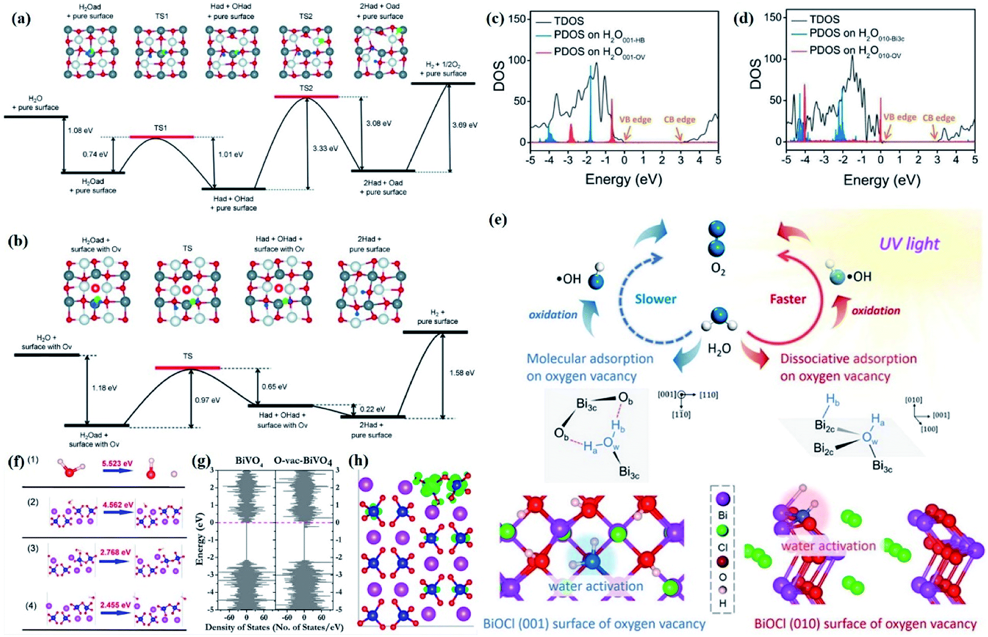 | ||
Fig. 13 Overall total-energy profile of the  reaction on a (a) pure BiOCl(001) surface and (b) BiOCl(001) surface with surface oxygen vacancies. Surface Bi, subsurface Bi, surface O, H atom of water and O atom of water are in white, grey, red, blue, and green, respectively. Red ring represents the surface oxygen vacancy.161 Copyright 2015 Wiley. PDOS of H2O on the (c) (001) and (d) (010) surfaces of BiOCl with different adsorption structures. (e) Theoretical study of water adsorption on the BiOCl (001) and BiOCl (010) surfaces with an OV and corresponding activation process.97 Copyright 2016 American Chemical Society. (f) Dissociation energies of a H2O molecule: (1) dissociation of a free H2O molecule; (2) dissociation of a H2O molecule on the BiVO4 surface of the (010) plane; (3 and 4) dissociation of a H2O molecule on the BiVO4 surface of the (010) plane with VO. (g) Calculated DOS of BiVO4 without and with VO on the surface of the (010) plane. The Fermi energy level was adjusted to 0 and is marked as a pink dashed line. (h) Charge density distribution at the Fermi level of BiVO4 with VO on the surface of the (010) plane.98 Copyright 2018 American Chemical Society. reaction on a (a) pure BiOCl(001) surface and (b) BiOCl(001) surface with surface oxygen vacancies. Surface Bi, subsurface Bi, surface O, H atom of water and O atom of water are in white, grey, red, blue, and green, respectively. Red ring represents the surface oxygen vacancy.161 Copyright 2015 Wiley. PDOS of H2O on the (c) (001) and (d) (010) surfaces of BiOCl with different adsorption structures. (e) Theoretical study of water adsorption on the BiOCl (001) and BiOCl (010) surfaces with an OV and corresponding activation process.97 Copyright 2016 American Chemical Society. (f) Dissociation energies of a H2O molecule: (1) dissociation of a free H2O molecule; (2) dissociation of a H2O molecule on the BiVO4 surface of the (010) plane; (3 and 4) dissociation of a H2O molecule on the BiVO4 surface of the (010) plane with VO. (g) Calculated DOS of BiVO4 without and with VO on the surface of the (010) plane. The Fermi energy level was adjusted to 0 and is marked as a pink dashed line. (h) Charge density distribution at the Fermi level of BiVO4 with VO on the surface of the (010) plane.98 Copyright 2018 American Chemical Society. | ||
Similarly, surface defect-induced adsorption and activation is also suitable for the oxygen evolution reaction, as demonstrated by bismuth vacancy mediated ultrathin Bi2WO6 nanosheets.162 Intriguingly, the work by Li et al. proposed that the H2O molecule activation was strongly determined by the structure of surface OVs.97 The upshifted PDOS of dissociatively adsorbed H2O on the (010) facet of BiOCl indicates that the activated H2O molecules are more prone to be oxidized on the OV of (010) facets than that of (001) facets, which can be further demonstrated by EPR analysis (Fig. 13c and d). In addition, the barrier breaking for the O–H bond in the OVs of (010) facets is smaller than that of (001) facets, and more electrons in OVs can be transferred to dissociatively adsorbed water on the (010) facets, giving rise to a higher level of OV-induced H2O molecule activation on the (010) facet of BiOCl (Fig. 13e).
Notably, in addition to the positive role of defects in the adsorption and activation of H2O molecules, the exciton behavior in defective semiconductors should also be evaluated after reducing the thickness to the atomic scale. With ultrathin BiVO4 nanosheets as a model semiconductor, for example, Dong et al. demonstrated the synergy of exposed active facets and oxygen vacancies on exciton dissociation.98 Theoretical analysis shows that not only the CB edge is extended to the Fermi level, but also the electronic densities of states at the CB minimum and VB maximum are increased after confining OVs onto the (010) facets of BiVO4 (Fig. 13g and h). Moreover, introducing OVs can also reduce the dissociation energies of H2O molecules, which improves the efficiency of H2O splitting into H and O atoms (Fig. 13f). Due to these positive alterations, the ultrathin BiVO4 nanosheets display the highest photocatalytic performance for oxygen evolution without cocatalysts, which can also be effectively used for overall water splitting upon further combination with a hydrogen-evolving photocatalyst and redox mediator.
Currently, the most commonly used method to improve the photocatalytic performance of two separate half reactions (hydrogen evolution and oxygen evolution) is to add sacrificial agents to suppress the opposite half-reaction or use a cocatalyst to transfer the photoinduced species required for the opposite half reaction. Worse still, the sacrificial agent inevitably expedites the separation of the intrinsic photogenerated charge carriers in the photocatalyst, which undoubtedly increases the difficulty of evaluating the mechanism of the actual photocatalytic water splitting process. That is to say, the obtained hydrogen and/or oxygen yield can only reflect the photocatalytic performance rather than the intrinsic properties of photocatalysts, and thus further research should focus on the overall water splitting without a sacrificial agent. Moreover, in order to improve the overall quantum efficiencies, one bottleneck to be overcome is balancing the photogenerated electron transfer between the two half reactions, so that two electrons participate in the hydrogen evolution reaction and four electrons participate in the oxygen evolution reaction.
5.2 Molecular oxygen activation
Molecular oxygen is the most eco-friendly and lowest cost natural oxidant, yet cannot directly participate in chemical reactions and oxidize other molecules under environmental conditions due to spin forbidden reactions.163 Fortunately, theory and experiments have uncovered that the relatively inert oxygen molecules in the ground state can be activated to highly reactive oxygen-involved species with the assistance of photoexcited electrons. These reactive oxygen-involved species, including singlet oxygen (1O2), superoxide anion radicals (˙O2−), hydrogen peroxide (H2O2), and hydroxyl radicals (˙OH), exhibit great potential for organic pollutant degradation.164 In fact, all photoinduced photocatalytic processes associated with the generation of reactive oxygen species can be classified as photocatalytic molecular oxygen activation. However, the molecular oxygen activation efficiency in actual reactions is often much lower than theoretical expectations, as a result of the kinetically persistent or spin-forbidden nature of triplet ground state molecular oxygen.165,166 Given the complication of molecular oxygen activation, which involves photons, hot carriers (electrons and holes) and neutral excitons (electron–hole pairs), the generation of reactive oxygen species is strongly determined by charge carrier mobility. To this end, the behavior of charge carriers on the surface and interface in a certain photocatalytic system should be clarified for manipulating the molecular oxygen activation reaction in a better manner.Normally, surface OVs with abundant localized electrons and dangling bonds are widely recognized to modulate the atomic coordination mode and electronic structure between the adsorbates and the surface.167 For instance, the interaction between fully oxidized surface and molecular oxygen is rather poor under ambient conditions, while the localized electrons near the surface OVs are able to charge molecular oxygen with a different number of electrons, with diverse activated oxygen products.168,169 Those activated oxygen molecules with strong oxidized capacity can participate in various oxidation reactions. However, little attention has been paid to the interaction between coordinately unsaturated metal atoms and molecules in the photocatalytic process. The coordinately unsaturated metal atoms with excess electrons can provide sites for oxygen molecular chemisorption, which builds a bridge for electron transfer from metal atoms to adsorbed oxygen molecules, resulting in the formation of various reactive oxygen-involved species. For instance, Di et al. proposed that the boosted reactive oxygen species within defect-rich BiOCl is not only due to the enhanced charge separation efficiency caused by surface pit defects (Fig. 14a), but also attributed to the positive role of low coordinated edge atoms along the defects that can promote the light absorption ability.52 More importantly, coordination-unsaturated Bi atoms can provide active sites for adsorbed oxygen molecule activation, which accelerates the generation of reactive oxygen species, resulting in improved photocatalytic performance (Fig. 14b and c).
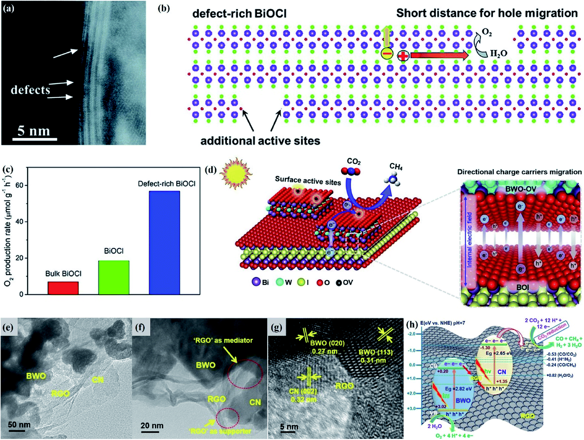 | ||
| Fig. 14 (a) TEM images of the defect-rich BiOCl ultrathin nanosheets. (b) Front view of atomically thin defect-rich BiOCl. (c) Photocatalytic oxygen evolution from water under 300 W Xe lamp irradiation for BiOCl and defect-rich BiOCl.52 Copyright 2017 Royal Society of Chemistry. (d) Schematic illustration for the proposed mechanism of photocatalytic CO2 reduction over the as-developed Bi2WO6-OV/BOI nanocomposite.175 Copyright 2019 Elsevier. (e) TEM and (f and g) HRTEM images of Bi2WO6/RGO/g-C3N4 with 15 wt% of Bi2WO6 with respect to g-C3N4. (h) Schematic of the Z-scheme charge transfer route in a Bi2WO6/RGO/g-C3N4 hybrid heterojunction.178 Copyright 2018 Elsevier. | ||
In analogy to the photoexcitation process, the molecular oxygen activation pathway is highly dependent on the involved photocatalytic process. To be specific, the generation mechanism of 1O2 in a photosensitization system is attributed to the exciton-involved resonance energy transfer process to alleviate the spin-flip restrictions of spin-triplet excitons. In the case of a carrier-dominated photocatalytic process, molecular oxygen is reduced to ˙O2−, O22−, or O42−, of which ˙O2− can be oxidized to 1O2 by holes. Given such a distinct mechanism towards 1O2 generation, the investigation on the influence of excitonic effects concerning molecular oxygen activation is indispensable. For example, Wang et al. proposed facet-related molecular oxygen activation behaviors within BiOBr, and found that the dominant reactive oxygen species on (001) and (010) facets are 1O2 and H2O2, respectively.112 This distinct mechanism is attributed to the fact that the excitons yield on (001) facets is much higher than that of (010) facets, resulting in a faint hot-carrier process in the sample with (001) facet exposure given by the competitive generation of excitons and hot carriers. Benefiting from the boosted 1O2 production, the BiOBr(001) sample displayed a higher selectivity and efficiency towards the sulfoxidation reaction compared with its counterpart BiOBr(010). Motivated by this, the reactive oxygen-involved photocatalytic pathway can be regulated by adjusting the photoexcitation process of semiconductors.
5.3 Carbon dioxide reduction
The direct impact of fossil fuels combustion on the environment is the fast-growing CO2 emission. Accumulative reports uncovered that photocatalytic CO2 reduction has great potential in alleviating negative effects, with carbon monoxide (CO) or high-value-added hydrocarbon compounds (e.g., CH4, C2H6, CH3OH, HCHO, HCOOH, C2H5OH, etc.) as reduction products. Thermodynamically, a proton-assisted multi-electron reduction process is more favorable than that of one-electron from CO2 to ˙CO2−, because the one-electron reduction reaction requires a very negative reduction potential (−1.9 eV).170,171 However, different from previous H2O molecules, the C![[double bond, length as m-dash]](https://www.rsc.org/images/entities/char_e001.gif) O double bond with high binding energy imparts excellent stability to CO2, which poses a formidable challenge to the activation of CO2. For a given CO2 reduction reaction, the adsorption ability of CO2 on the photocatalyst surface determines the retention time of CO2 on the surface, which will ultimately affect the activation efficiency of CO2 molecules. In view of this, the surface properties of the photocatalyst, such as surface atom arrangement, coordination mode and charge potential, greatly determine the active sites of CO2 adsorption and activation.
O double bond with high binding energy imparts excellent stability to CO2, which poses a formidable challenge to the activation of CO2. For a given CO2 reduction reaction, the adsorption ability of CO2 on the photocatalyst surface determines the retention time of CO2 on the surface, which will ultimately affect the activation efficiency of CO2 molecules. In view of this, the surface properties of the photocatalyst, such as surface atom arrangement, coordination mode and charge potential, greatly determine the active sites of CO2 adsorption and activation.
Due to the structural sensitivity of OVs, the introduction of surface OVs will result in localized atom relaxations, leading to surface atomic rearrangement and band structure regulation. This change is demonstrated to be favorable for inert CO2 chemisorption, thereby facilitating the subsequent activation process. For instance, Liu et al. reported that the surface state and electronic structure of Bi4Ti3O12 ultrathin nanosheets are greatly optimized after embedding OVs onto the surface, which promotes the adsorption of CO2.172 In view of the diversity of CO2 reduction products, the relationship between surface OVs and product selectivity should also be illustrated. By analyzing the solid–gas interface reaction, only CO is detected in perfect Bi2MoO6, while a fairly high yield of CH4 is generated in defective Bi2MoO6, and all defective Bi2MoO6 with different OV concentrations exhibits a higher CH4 selectivity than perfect samples.110 Such OV-induced CH4 selectivity towards CO2 reduction is attributed to the fact that OVs can act as active sites for CO2 adsorption in a bidentate carbonate mode, which thermodynamically supports the conversion from intermediate CO* to *CHO, and then to CH4 through a series of hydrogenation processes. Similar improved CO2 adsorption induced by surface defects also exists in ultrathin Bi2MoO6 nanosheets with “Bi–O” vacancy pairs.109 Besides, the diversity of crystal facets caused by different atomic configurations will result in diverse surface properties, such as polarity and Lewis basicity, which are also a predominant factor to be considered when evaluating the adsorption and activation of CO2 on the photocatalyst surface.173 For instance, BiOI nanosheets with different dominant facets, (001) and (100) facets, were prepared via adjusting the reaction time of the hydrothermal process.174 As compared to BiOI-001, the BiOI-100 sample displays much improved photocatalytic CO2 reduction performance. Such facet-dependent performance is attributed to the improved carrier separation efficiency, as a result of internal electric fields perpendicular to the dominant (100) facets in the BiOI-100 sample. Besides, the relatively higher CB position of the BiOI-100 sample is also favorable for the improvement of photocatalytic CO2 reduction.
Moreover, considering that the activation of CO2 is a proton-assisted multi-electron process, the charge separation efficiency also determines the conversion rates. For this reason, a common strategy is to construct heterojunctions by coupling two semiconductors with suitable a forbidden band width and band potentials. For instance, 2D–2D Bi2WO6/BiOI heterojunctions were constructed by assembling oxygen-deficient Bi2WO6 nanosheets onto BiOI nanosheets, which exhibited more outstanding photocatalytic performance for CO2 reduction than a single semiconductor.175 The improved photocatalytic performance is attributed to the synergistic effect of the p–n heterojunction and surface oxygen vacancies. The internal electric field close to the p–n heterointerface induces ultrafast directional transfer and spatial separation of photogenerated charge carriers, as indicated by the stronger transient photocurrent responses and smaller electron transfer resistance of the heterojunction sample than that of single semiconductors. Besides, the imperative roles of oxygen vacancies of Bi2WO6 cannot be ignored, which not only induce a second electron transfer from the CB of Bi2WO6 to the its oxygen vacancy-defect state, but also function as adsorption and activation sites for initiating the surface CO2 reduction reaction (Fig. 14d). Consequently, these propitious properties endow the heterojunction samples with superior photocatalytic performance compared to the individual components. Nevertheless, the improved charge separation efficiency in these traditional heterojunctions is usually achieved by sacrificing the high-energy electrons of semiconductors with strong reduction potentials, which not only weakens the reduction ability of photogenerated electrons, but also inevitably leads to the loss of electrons during the interface transfer, thereby resulting in a relatively poor photocatalytic CO2 reduction efficiency.
To overcome these bottlenecks, Z-scheme heterojunctions composed of one reduction semiconductor with high reduction potential and one oxidation semiconductor with high oxidation potential have attracted much attention, where the transfer route of photogenerated charge carriers is similar to the letter “Z”, which can efficiently preserve the superior redox abilities of photogenerated charge carriers. In general, according to whether there is an electron mediator involved in the carrier transfer process, Z-scheme heterojunctions can be divided into two types: direct and indirect. In addition, depending on the species of the electron mediator, indirect Z-scheme heterojunctions are further subdivided into conventional liquid-phase and all-solid-state Z-scheme photocatalytic systems. With [Co(tpy)2]2+/3+ as an electron mediation, a liquid-phase Z-scheme system composed of [Ru(dpbpy)]/(CuGa)1−xZn2xS2 and BiVO4 was constructed to achieve the selective reduction of CO2 under visible light irradiation. Due to the efficient electron transfer from BiVO4 to [Ru(dpbpy)]/(CuGa)1−xZn2xS2 with the assistance of electron mediation, the CO2 reduction activity in the hybrid system is significantly higher than that of a single semiconductor.176 Also, the common I3−/I− redox mediator is also employed to construct a liquid-phase Z-scheme heterojunction to obtain excellent photocatalytic performance for CO2 conversion.177 Nevertheless, the overall photocatalytic activity is still limited by several factors, such as the backward reactions between redox mediators and reaction sites, a strong light shielding effect and relatively poor photostability. Bearing this in mind, all-solid-state Z-scheme photocatalysts with conductive materials as an electron bridge are developed to achieve fast interfacial charge transfer, where noble metals, carbon materials, etc. are employed as electron bridges. For example Jo and coworkers reported an all-solid-state Z-scheme Bi2WO6/RGO/g-C3N4 heterojunction for photocatalytic CO2 reduction, in which RGO works as an electron bridge to facilitate the recombination of the CB electrons of Bi2WO6 with the VB holes of g-C3N4 (Fig. 14e–h).178 As a result, the photogenerated electrons of g-C3N4 with a high reduction potential are retained to participate in the CO2 reduction reaction, with an optimal AQY of 0.75% at 400 nm. Similarly, some other all-solid-state Z-scheme photocatalysts, such as Bi2WO6/Au/CdS,179 BiVO4/C/Cu2O,180etc., also exhibit excellent photocatalytic performance with respect to photocatalytic CO2 reduction under visible light irradiation.
More recently, in order to further optimize the indirect Z-scheme photocatalytic system to obtain superior photocatalytic activity, direct Z-scheme heterojunctions with two semiconductors in intimate contact with each other are designed and applied to the field of photocatalytic CO2 reduction. Those direct Z-scheme systems not only inherit the advantages of indirect Z-scheme systems, but also greatly reduce the construction cost. Particularly, the internal electric filed generated from the staggered band alignment of two components can play the same role as the electron mediator to promote the recombination of charge carriers with a relatively poor redox ability, leaving strong individual redox abilities of two components. Combining all these merits, the direct Z-scheme system exhibits greater potential for photocatalytic CO2 reduction compared with those indirect systems. For instance, Wang et al. prepared a direct Z-scheme heterojunction composed of CsPbBr3 quantum dots (QDs) and Bi2WO6 nanosheets, which showed improved performance towards photocatalytic CO2 reduction as compared to single components.181 Such enhanced activity is attributed to the efficient charge separation and retention of high-energy electrons at the CsPbBr3 side, as a result of the Z-scheme charge carrier transfer mechanism. Taking another example, a direct Z-scheme CdS/BiVO4 heterojunction was prepared and used for photocatalytic CO2 reduction.182 Due to the fast recombination of weaker reductive electrons and oxidative holes, the photogenerated electrons with a more negative potential can be accumulated in the CB of CdS to initiate the surface CO2 reduction reaction, giving rise to an improved photocatalytic performance in heterojunction samples.
Overall, constructing a direct Z-scheme heterojunction can accelerate the charge transfer and separation, and preserve the strong redox ability of photogenerated charge carriers, which is favorable for the activation of CO2 molecules. Notably, the desorption of CO2 reduction products on the surface of photocatalysts is also a critical factor in determining the photocatalytic performance of CO2 reduction outside of CO2 adsorption and charge carrier separation efficiency, because the timely desorption of the product from the photocatalyst surface can guarantee that there are enough active sites for continuous photocatalytic reactions.183 To this end, the profound investigation on the structure–activity relationship between surface properties and corresponding photocatalytic performance is a prerequisite for designing and preparing photocatalysts with high photocatalytic activity for CO2 reduction.
5.4 Nitrogen fixation
Nitrogen fixation refers to the process of converting molecular nitrogen into nitrogen-containing compounds such as ammonia, hydrazine and nitrate, which can produce materials essential for agriculture and industry. As compared to the traditional Haber–Bosch nitrogen fixation process, which requires harsh conditions (high pressure and high temperature) to overcome the energy barriers, the solar-driven nitrogen fixation process displays unlimited potential for alternative artificial nitrogen fixation.184 Nevertheless, the state-of-the-art reduction rate is still limited by intrinsically sluggish N![[triple bond, length as m-dash]](https://www.rsc.org/images/entities/char_e002.gif) N bond activation kinetics, and insufficient charge carriers for NN bond broking and water oxidation. With these properties in mind, in order to obtain high quantum yields, the surface should provide as many as possible active sites for N2 adsorption, and the generated electrons should be negative enough to initiate the N2 reduction reaction on the photocatalyst surface.
N bond activation kinetics, and insufficient charge carriers for NN bond broking and water oxidation. With these properties in mind, in order to obtain high quantum yields, the surface should provide as many as possible active sites for N2 adsorption, and the generated electrons should be negative enough to initiate the N2 reduction reaction on the photocatalyst surface.
Modern material characterization techniques and theoretical calculation simulations demonstrate that the overall activity of heterogeneous photocatalysts is predominantly determined by the surface structures, especially defects.25 In general, the surface defects, mainly referring to the introduction of vacancies and/or heteroatom doping, have demonstrated to be an effective strategy for the adsorption and activation of nitrogen molecules. Similar to the case of CO2 reduction, the introduction of OVs is also beneficial to the adsorption of inert N2 molecules, and the surrounded electron-rich cations can transfer electrons to adsorbed N2 to initiate the reduction reaction. To corroborate this point, Zhang et al. prepared BiOBr nanosheets through a solvothermal method, and confined OVs on their (001) facets through releasing terminated oxygen atoms.111 Theoretical calculations validate that the adsorption of N2 on the OVs follows an end-on bound model with N2 molecules connected to two OV-connected and partially reduced Bi atoms, while the activation of N2 is attributed to the electron back-donation behavior of OVs. As demonstrated by steady-state and time-resolved photoluminescence spectroscopy, the photogenerated electrons are firstly captured by OVs, followed by interfacial electron transfer to the adsorbed N2 through the π-back-donation behavior induced by the localized electrons of OVs. Due to the efficient adsorption and interfacial electron back-donation phenomenon induced by surface oxygen vacancies, BiOBr-001-OV displays a higher photocatalytic N2 fixation rate than any other reported catalysts. However, another study proposed that the distinct N2 activation pathway is due to the different vacancy types of different facets, with BiOCl exposed by (010) and (001) facets as an example.184 More interestingly, an interfacial charging–discharging mechanism is proposed to explain the pathway of N2 activation (Fig. 15a). During the charging process, the oxygen vacancies on the (010) facets can activate the adsorbed O2 to O22− by localizing two electrons, while only one electron can be localized on the (001) surface to generate ˙O2−. Accordingly, due to the totally divergent geometric structures of
  and
and  , the oxygen-vacancy-mediated discharging process and oxidation products on (010) and (001) facets are significantly distinct (Fig. 15b–e). That is, during the discharging process, one of the two electrons of O22− of (010) facets is back-donated to VO to generate a new
  , accompanied by the first round of NO oxidation, followed by a second round of NO oxidation initiated by
  . While
  -induced NO oxidation on the (001) facets is monodentate rather than bidentate nitrate emerged as the product (Fig. 15f).
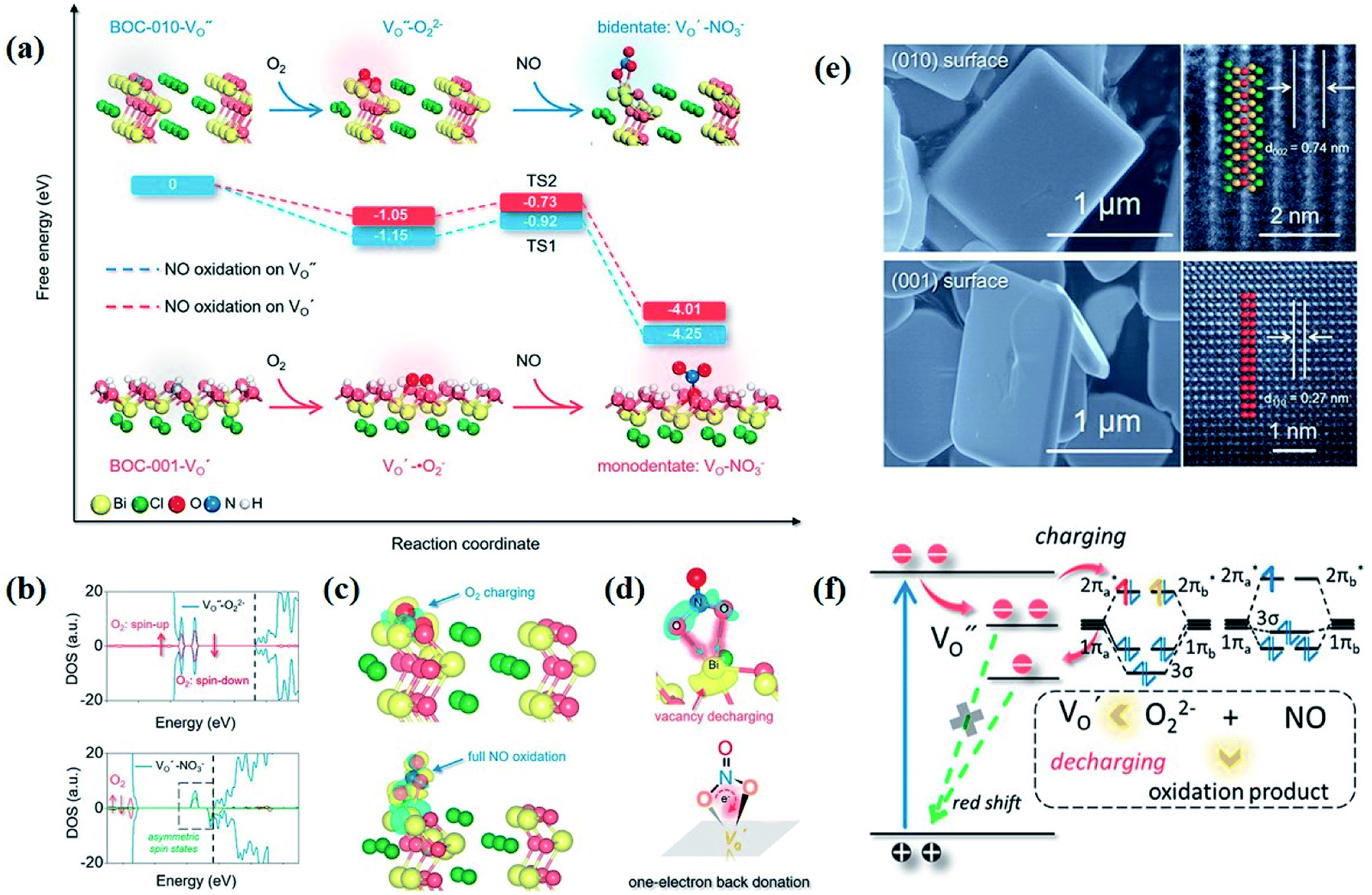 | ||
Fig. 15 (a) Free energy change during O22−- and ˙O2−-mediated NO oxidation on the VO of BOC-010 and BOC-001, respectively. TS represents the transition state. (b) DOS of O22−-adsorbed and NO3−-adsorbed BOC-010 with VO. Vertical dashed line in the DOS shows the CBM. (c) Charge density difference of O22−-adsorbed and NO3−-adsorbed BOC-010 with VO. (d) Regional charge density difference between O22− and VO on BOC-010. (e) SEM and atomic-resolution HAADF-STEM images of BOC-010 and BOC-001. (f) Schematic illustration of the charging–discharging scheme on the  of BOC-010.184 Copyright 2019 American Chemical Society. of BOC-010.184 Copyright 2019 American Chemical Society. | ||
Aside from the above facet-associated divergence in the properties of surface oxygen vacancies, heteroatom doping also influences the electric structure of the host crystal, thereby determining the adsorption and activation behaviors of N2. For instance, Zhang et al. reported that the N2 fixation efficiency was a function of Fe doping content rather than solely related to oxygen vacancies, showing a volcano-type activity.185 Although the potential of CB electrons of BiOCl is not negative enough to directly reduce N2, the surface OVs promote the chemisorption of N2 and weakened NN by injecting electrons into the antibonding π-orbitals. Particularly, the photocatalytic performance is greatly improved after the introduction of Fe dopants, which is due to the fact that Fe doping strengthened the interaction between the adsorbate and catalysts, as evidenced by the smaller d-band center of BiOCl NSs-Fe-5% than the undoped sample. The strengthened binding strength is also validated by higher desorption temperatures of BiOCl NSs-Fe-5% than pure BiOCl. However, the Fe content should be strictly controlled, as an excessive Fe content may introduce undesired lattice disorder acting as a charge recombination center, thereby resulting in a decreased N2 fixation efficiency. Similarly, Meng et al. reported that Fe doping can reduce the surface work function of Bi2MoO6, which is favorable for the charge carrier transfer to the surface. More interestingly, they also find that the introduced Fe3+/Fe2+ redox pathway can serve as the surface center for N2 reduction, and thus the Fe-doped Bi2MoO6 photocatalyst displayed excellent photocatalytic N2 fixation performance under visible light irradiation.186
It should be noted that, beyond available electrons for N2 reduction reactions, the overall N2 fixation efficiency is also determined by proton transfer that greatly affects the interfacial electron transfer. Moreover, the investigation on the thermodynamic effect of OVs towards photocatalytic N2 fixation is critical for unfolding how OVs overcome the kinetic inertia of N2 fixation. In light of this, Li and co-workers evaluated the facet-dependent influence of OVs on the surface-N2 interactions and the thermodynamic reaction pathways of N2 fixation, using BiOCl nanosheets with (001) and (010) facet exposure as the prototypical catalyst.187 DFT calculations show that the N2 adsorption model on the (001) and (010) facets follows terminal end-on and side-on bridging adsorption models, respectively, of which side-on binding mode with a decreased bond order and longer bond length exhibits a larger extent of N2 activation. Based on thermodynamic reaction pathway analysis, it is demonstrated that OV-mediated N2 reduction on the (001) facet is initiated by an asymmetric distal mode, with NH3 as the only products. Inversely, the N2 fixation on the (010) facet proceeds in a symmetric alternating pathway, with N2H4 as the main intermediate.
6. Summary and outlook
With moderate band gap structures and unique electronic structures, exploring the potential of Bi-based materials is increasing to an unprecedented height and will remain a critical research direction for photocatalytic molecules activation. Moreover, given the special geometry of 2D nanomaterials, the construction ofz2D Bi-based photocatalysts usually involves delicate engineering at the atomic level. As a special structural feature of 2D Bi-based photocatalysts, the decreased size in the third dimension, provides unique engineering protocols with respect to regulating the surface or interface properties. In this focus review, various surface and interface parameters related to the generation, mobility, and consumption of photoinduced charge carriers in a photocatalytic system as well as their interplay relationships are thoroughly stated in the first place, which can provide guidance for the design and optimization of 2D Bi-based photocatalysts with engineered surfaces and interfaces. According to surface and interface parameters, the prepared 2D Bi-based photocatalyst with varying structural features, such as defects, thickness, facets, doping, and surface pores, will result in distinct photocatalytic performance. In order to gain insight into the structure-dependent performance, various advanced characterization techniques are used to clearly visualize the fine structure of photocatalysts at the atomic level. In the following section, various engineering protocols with surface and interface parameters taken into account are summarized, with the aim to give rise to an improved photocatalytic performance. By virtue of the optimized surface and interface properties, 2D Bi-based photocatalysts have been widely employed to active various molecules, such as CO2, N2, O2 and H2O, under visible light irradiation to alleviate energy shortages and alleviate pollution. Different from other reported applications, this section sheds light on illustrating the indispensable role of surfaces and interfaces in the activation of ambient molecules in the photocatalytic process, and demonstrates that the performance of materials is a function of their precisely engineered structural characteristics.2D Bi-based photocatalysts with an appealing electric structure and large surface area provide a promising platform for gaining efficient solar energy utilization, and encouraging progress has been made. Nevertheless, there are also formidable challenges in specific photocatalytic reactions over these 2D Bi-based photocatalysts that deserve focus.
To begin with, although various methods for the synthesis of 2D Bi-based photocatalysts have been reviewed in many reported studies, no more detailed information is provided here, which does not mean that the state-of-the-art synthesis methods are mature. The major breakthroughs will come at the hands of exploring low-cost, highly effective and universal methods to prepare high-yield and massive 2D Bi-based photocatalysts for practical applications. Such a dilemma stems from the fact that current technologies and methods cannot accurately control the synthesized materials with desirable structures, because it is difficult to monitor the crystal growth process in real time. Accordingly, an urgent task is to carry out advanced in situ and operando monitoring at high spatial, spectral and temporal resolutions, so as to fundamentally reveal the evolution of 2D Bi-based photocatalysts on the atomic scale during environmental purification and energy conversion. Nowadays, several in situ high-technologies are developed, such as in situ IR, in situ XAFS, in situ TEM, in situ XAS and so on. Among them, in situ IR spectroscopy is the most widely applied approach to monitor the dynamic evolution of reaction intermediates, so as to reveal the reaction pathway and mechanism. However, it is still a technical challenge to carrier out in situ IR spectroscopic studies in aqueous systems, owing to the strong IR absorption by water molecules. In addition, the information obtained from experiments is extremely limited since a photocatalytic reaction is so rapid and complicated that it is difficult to detect various intermediate products produced during the reaction in a short time. More recently, big data based on experiments and calculations have promoted the development of mechanical learning methodologies, making them show unlimited potential in discovering various functional materials. Inspired by this, further efforts should focus on feeding the data obtained from in situ studies into mechanical learning methodologies to predict potential photocatalysts and effective photocatalytic systems.
Next, in terms of charge kinetics, some special situation should be taken into account, such as the excitonic effects in 2D Bi-based photocatalysts. Fundamentally, the photoexcitation process can be explained by energy band theory, that is, the photocatalyst adsorbs photons with energy larger than its band gap to generate excited electrons and holes, followed by transferring to the surface for surface reactions or recombination with each other in the bulk. However, in some case, the behavior of charge carriers fails to explain the photoexcitation process. As for 2D Bi-based photocatalysts, the Coulomb interactions between electrons and holes are significantly stronger than that of bulk counterparts, which may induce the generation of excitons. In this case, the excitonic effects should be considered when identifying the mechanism of the photoexcitation process, especially for those 2D Bi-based materials with strong excitonic effects. In addition, as for exciton-involved photocatalytic reactions, the effective methods should be explored to regulate the exciton behavior to eliminate the excitonic effects on the photocatalytic performance in 2D Bi-based photocatalysts.
Then, given the fast recombination of photogenerated electrons and holes, strenuous efforts are devoted to constructing 2D–2D heterojunctions. As compared with the lateral interface, the basal interface exhibits more significant advantages, such as a larger surface area, strengthened interaction, and lower resistivity, which makes it an eye-catching candidate for ameliorating charge separation efficiency through interface engineering. However, one challenge is maintaining the stability of this stacked structure. As compared to electrostatic interaction, van der Waals interaction and chemical bond interaction are relatively more stable, and thus further development in this aspect should be devoted to the design and construction of basal plane 2D–2D heterojunctions with strong interface interaction.
Afterwards, as demonstrated above, surface and/or interface engineering show great potential for manipulating the design, synthesis and reaction kinetics of a specific photocatalytic system. It is noteworthy that the optimized photocatalyst design is accompanied by multiple modifications of the physicochemical properties of photocatalysts. For instance, the introduction of oxygen vacancies not only promotes the adsorption and activation of N2, but also improves the light absorption ability, both of which contribute to the enhancement of the overall photocatalytic performance, which has been widely accepted. However, this cooperative contribution of multifarious factors to the activity improvement makes it difficult to identify the specific bottleneck of the photocatalytic reaction kinetics. In light of this, the ingenious design of a photocatalyst with spatially decoupled activity-contribution factors is beneficial to deconvolute the contribution of various factors to the overall photocatalytic performance.
What's more, since the overall photocatalytic performance is evaluated by the multiplication of various parameters involved on different time scales and spatial resolutions, the quantitative description of these parameter-related physicochemical properties to determine the contribution of each parameter to the enhancement of the overall photocatalytic performance can provide technical support for the design of highly active photocatalysts. As for a specific photocatalytic reaction, the overall photocatalytic performance is determined by photon absorption, exciton separation, carrier transfer, photocatalytic reaction efficiency, and mass transfer of reactants/products. DFT calculations still display remarkable merits in quantifying the effect of these parameters to the overall photocatalytic performance, which facilitates the design and screening of ideal semiconductors for photocatalytic applications. For instance, in terms of photon absorption that is dependent on the electronic structure of the semiconductor, the DOS based on the Franck–Condon principle can accurately dictate the optoelectronic properties of semiconductors by incorporating spin–orbit coupling into the accurate determination of the local crystal structure. As for exciton separation, the key point is to determine whether the exciton binding energy is lower than the benchmark energy value, and in this aspect, DFT calculation has proven to be a high-precision method for estimating the exciton binding energy and effective masses. Moreover, based on classical semiconductor device equations, simplified 2D numerical modeling can quantitatively describe the potential gradient of the semiconductor, which provides reliable estimation of quantum efficiency as a function of wavelength. Overall, simulation can predict maximum photocatalytic quantum efficiencies by identifying these quantified parameters involved in the photocatalytic process, which provides reliable guidance in altering material itself, optimizing the synthesis protocol or regulating other aspects to overcome the kinetic bottleneck.
Last but not least, in terms of practicality, the current Bi-based photocatalysts are in powder form, which makes the separation and recovery of the photocatalyst from the reaction system more tedious and sophisticated, thus limiting its practical application. In this regard, immobilizing a Bi-based film photocatalyst onto an arbitrary substrate is regarded a sustainable choice. In this circumstance, several aspects should be rationally designed: (i) the interfacial interaction between the film photocatalysts and the substrates to guarantee the durability for continuous applications; (ii) the hydrophilicity and surface structure of the film photocatalysts to promote the adsorption of reactants and the desorption of products. In addition to the material itself, the actual reaction conditions, such as temperature, pressure, solution and so on, may also influence the activity and durability of photocatalysts, which should be considered in the practical photoreactor design.
Conflicts of interest
There are no conflicts to declare.Acknowledgements
This study was financially supported by the Program for the National Natural Science Foundation of China (51879101, 51579098, 51779090, 51709101, 51521006, 51809090, 51278176, and 51378190), the National Program for Support of Top-Notch Young Professionals of China (2014), the Program for Changjiang Scholars and Innovative Research Team in University (IRT-13R17), the Hunan Provincial Science and Technology Plan Project (2018SK20410, 2017SK2243, and 2016RS3026), and the Fundamental Research Funds for the Central Universities (531109200027, 531107051080, 531107050978, and 531107051205).References
- T. Ma, S. Dai and S. Qiao, Mater. Today, 2016, 19, 265 CrossRef CAS.
- C. Gao, J. Wang, H. Xu and Y. Xiong, Chem. Soc. Rev., 2017, 46, 2799 RSC.
- D. Huang, S. Chen, G. Zeng, X. Gong, C. Zhou, M. Cheng, W. Xue, X. Yan and J. Li, Coord. Chem. Rev., 2019, 385, 44 CrossRef CAS.
- A. Fujishima and K. Honda, Nature, 1972, 238, 37 CrossRef CAS.
- W. Zhou, J. Guo, S. Shen, J. Pan, J. Tang, L. Chen, C. Au and S. Yin, Acta Phys.-Chim. Sin., 2020, 36, 1906048 Search PubMed.
- L. Lei, D. Huang, G. Zeng, M. Cheng, D. Jiang, C. Zhou, S. Chen and W. Wang, Coord. Chem. Rev., 2019, 399, 213020 CrossRef CAS.
- S. Sun, X. Zhang, X. Liu, L. Pan, X. Zhang and J. Zou, Acta Phys.-Chim. Sin., 2020, 36, 1905007 Search PubMed.
- S. Chen, D. Huang, G. Zeng, X. Gong, W. Xue, J. Li, Y. Yang, C. Zhou, Z. Li, X. Yan, T. Li and Q. Zhang, Chem. Eng. J., 2019, 370, 1087 CrossRef CAS.
- K. Novoselov, A. Geim, S. Morozov, D. Jiang, Y. Zhang, S. Dubonos, I. Grigorieva and A. Firsov, Science, 2004, 306, 666 CrossRef CAS.
- H. Zhang, ACS Nano, 2015, 9, 9451 CrossRef CAS.
- A. Geim and K. Novoselov, Nat. Mater., 2007, 6, 183 CrossRef CAS.
- M. Chhowalla, D. Jena and H. Zhang, Nat. Rev. Mater., 2016, 1, 16052 CrossRef CAS.
- F. Bonaccorso, L. Colombo, G. Yu, M. Stoller, V. Tozzini, A. Ferrari, R. Ruoff and V. Pellegrini, Science, 2015, 347, 41 CrossRef CAS.
- S. Chen, D. Huang, P. Xu, W. Xue, L. Lei, M. Cheng, R. Wang, X. Liu and R. Deng, J. Mater. Chem. A, 2020, 8, 2286 RSC.
- D. Voiry, J. Yang and M. Chhowalla, Adv. Mater., 2016, 28, 6197 CrossRef CAS.
- Y. Dai, P. Ren, Y. Li, D. Lv, Y. Shen, Y. Li, H. Niemantsverdriet, F. Besenbacher, H. Xiang, W. Hao, N. Lock, X. Wen, J. Lewis and R. Su, Angew. Chem., Int. Ed., 2019, 58, 6265 CrossRef CAS.
- S. Chen, D. Huang, G. Zeng, W. Xue, L. Lei, P. Xu, R. Deng, J. Li and M. Cheng, Chem. Eng. J., 2020, 382, 122840 CrossRef CAS.
- R. He, D. Xu, B. Cheng, J. Yu and W. Ho, Nanoscale Horiz., 2018, 3, 464 RSC.
- K. Xu, L. Wang, X. Xu, S. Dou, W. Hao and Y. Du, Energy Storage Materials, 2019, 19, 446 CrossRef.
- H. Feng, Y. Du, C. Wang and W. Hao, Curr. Opin. Green Sustain. Chem., 2017, 6, 93 CrossRef.
- Z. Xu, K. Xu, H. Feng, Y. Du and W. Hao, Sci. Bull., 2018, 63, 465 CrossRef CAS.
- S. Zhang, M. Xie, F. Li, Z. Yan, Y. Li, E. Kan, W. Liu, Z. Chen and H. Zeng, Angew. Chem., Int. Ed., 2016, 55, 1666 CrossRef CAS.
- S. Cao, B. Shen, T. Tong, J. Fu and J. Yu, Adv. Funct. Mater., 2018, 28, 1800136 CrossRef.
- S. Zhao, Z. Dai, W. Guo, F. Chen, Y. Liu and R. Chen, Appl. Catal., B, 2019, 244, 206 CrossRef CAS.
- Y. Huang, N. Zhang, Z. Wu and X. Xie, J. Mater. Chem. A, 2020, 8, 4978 RSC.
- H. Yu, L. Jiang, H. Wang, B. Huang, X. Yuan, J. Huang, J. Zhang and G. Zeng, Small, 2019, 15, 1901008 CrossRef.
- L. Ye, Y. Deng, L. Wang, H. Xie and F. Su, ChemSusChem, 2019, 12, 3671 CrossRef CAS.
- J. Xiong, P. Song, J. Di, H. Li and Z. Liu, J. Mater. Chem. A, 2019, 7, 25203 RSC.
- J. Di, J. Xia, H. Li, S. Guo and S. Dai, Nano Energy, 2017, 41, 172 CrossRef CAS.
- X. Jin, L. Ye, H. Xie and G. Chen, Coord. Chem. Rev., 2017, 349, 84 CrossRef CAS.
- C. Xie, Z. Niu, D. Kim, M. Li and P. Yang, Chem. Rev., 2020, 120, 1184 CrossRef CAS.
- S. Chen, D. Huang, P. Xu, X. Gong, W. Xue, L. Lei, R. Deng, J. Li and Z. Li, ACS Catal., 2020, 10, 1024 CrossRef CAS.
- S. Bai, J. Jiang, Q. Zhang and Y. Xiong, Chem. Soc. Rev., 2015, 44, 2893 RSC.
- H. Tong, S. Ouyang, Y. Bi, N. Umezawa, M. Oshikiri and J. Ye, Adv. Mater., 2012, 24, 229 CrossRef CAS.
- M. Batzill, Energy Environ. Sci., 2011, 4, 3275 RSC.
- A. Cherevan, P. Gebhardt, C. Shearer, M. Matsukawa, K. Domen and D. Eder, Energy Environ. Sci., 2014, 7, 791 RSC.
- H. Zhang, L. Yang, Z. Liu, M. Ge, Z. Zhou, W. Chen, Q. Li and L. Liu, J. Mater. Chem., 2012, 22, 18572 RSC.
- M. Pan, H. Zhang, G. Gao, L. Liu and W. Chen, Environ. Sci. Technol., 2015, 49, 6240 CrossRef CAS.
- H. Zhang, L. Liu and Z. Zhou, RSC Adv., 2012, 2, 9224 RSC.
- L. Ye, L. Zan, L. Tian, T. Peng and J. Zhang, Chem. Commun., 2011, 47, 6951 RSC.
- H. Yang, C. Sun, S. Qiao, J. Zou, G. Liu, S. Smith, H. Cheng and G. Lu, Nature, 2008, 453, 638 CrossRef CAS.
- J. Jiang, K. Zhao, X. Xiao and L. Zhang, J. Am. Chem. Soc., 2012, 134, 4473 CrossRef CAS.
- H. Zhang, Y. Yang, Z. Zhou, Y. Zhao and L. Liu, J. Phys. Chem. C, 2014, 118, 14662 CrossRef CAS.
- Y. Bai, L. Ye, T. Chen, L. Wang, X. Shi, X. Zhang and D. Chen, ACS Appl. Mater. Interfaces, 2016, 8, 27661 CrossRef CAS.
- J. Li, L. Zhang, Y. Li and Y. Yu, Nanoscale, 2014, 6, 167 RSC.
- H. Zheng, J. Ou, M. Strano, R. Kaner, A. Mitchell and K. Kalantar-Zadeh, Adv. Funct. Mater., 2011, 21, 2175 CrossRef CAS.
- G. Li, G. Blake and T. Palstra, Chem. Soc. Rev., 2017, 46, 1693 RSC.
- J. Li, H. Li, G. Zhan and L. Zhang, Acc. Chem. Res., 2017, 50, 112 CrossRef CAS.
- H. Huang, S. Tu, C. Zeng, T. Zhang, A. Reshak and Y. Zhang, Angew. Chem., Int. Ed., 2017, 56, 11860 CrossRef CAS.
- C. Xu, P. Qiu, L. Li, H. Chen, F. Jiang and X. Wang, ACS Appl. Mater. Interfaces, 2018, 10, 25321 CrossRef CAS.
- B. Xu, Y. Gao, Y. Li, S. Liu, D. Lv, S. Zhao, H. Gao, G. Yang, N. Li and L. Ge, Appl. Surf. Sci., 2020, 507, 144806 CrossRef CAS.
- M. Li, Y. Zhang, X. Li, Y. Wang, F. Dong, L. Ye, S. Yu and H. Huang, ACS Sustainable Chem. Eng., 2018, 6, 2395 CrossRef CAS.
- X. Li, W. Zhang, J. Li, G. Jiang, Y. Zhou, S. Lee and F. Dong, Appl. Catal., B, 2019, 241, 187 CrossRef CAS.
- S. Wendt, P. Sprunger, E. Lira, G. Madsen, Z. Li, J. Hansen, J. Matthiesen, A. Blekinge-Rasmussen, E. Laegsgaard, B. Hammer and F. Besenbacher, Science, 2008, 320, 1755 CrossRef CAS.
- N. Zhang, X. Li, H. Ye, S. Chen, H. Ju, D. Liu, Y. Lin, Y. Wei, C. Wang, X. Qian, J. Zhu, L. Song, J. Jiang and Y. Xiong, J. Am. Chem. Soc., 2016, 138, 8928 CrossRef CAS.
- Z. Song, X. Dong, J. Fang, C. Xiong, N. Wang and X. Tang, J. Hazard. Mater., 2019, 377, 371 CrossRef CAS.
- M. Guan, C. Xiao, J. Zhang, S. Fan, R. An, Q. Cheng, J. Xie, M. Zhou, B. Ye and Y. Xie, J. Am. Chem. Soc., 2013, 135, 10411 CrossRef CAS.
- J. Cai, A. Cao, J. Huang, W. Jin, J. Zhang and Z. Jiang, Appl. Catal., B, 2020, 267, 118378 CrossRef CAS.
- Y. He, O. Dulub, H. Cheng, A. Selloni and U. Diebold, Phys. Rev. Lett., 2009, 102, 106105 CrossRef.
- H. Huang, C. Zhou, X. Jiao, H. Yuan, J. Zhao, C. He, J. Hofkens, M. Roeffaers, J. Long and J. Steele, ACS Catal., 2020, 10, 1439 CrossRef CAS.
- S. Guo, X. Zhu, H. Zhang, B. Gu, W. Chen, L. Liu and P. Alvarez, Environ. Sci. Technol., 2018, 52, 6872 CrossRef CAS.
- L. Zhang, Y. Shi, Z. Wang, C. Hu, B. Shi and X. Cao, Appl. Catal., B, 2020, 265, 118563 CrossRef.
- J. Tian, P. Hao, N. Wei, H. Cui and H. Liu, ACS Catal., 2015, 5, 4530 CrossRef CAS.
- Y. Shi, X. Xiong, S. Ding, X. Liu, Q. Jiang and J. Hu, Appl. Catal., B, 2018, 220, 570 CrossRef CAS.
- H. Li, J. Li, Z. Ai, F. Jia and L. Zhang, Angew. Chem., Int. Ed., 2018, 57, 122 CrossRef CAS.
- K. Zhao, L. Zhang, J. Wang, Q. Li, W. He and J. Yin, J. Am. Chem. Soc., 2013, 135, 15750 CrossRef CAS.
- H. Li, J. Shi, K. Zhao and L. Zhang, Nanoscale, 2014, 6, 14168 RSC.
- C. Mao, H. Cheng, H. Tian, H. Li, W. Xiao, H. Xu, J. Zhao and L. Zhang, Appl. Catal., B, 2018, 228, 87 CrossRef CAS.
- J. Li, X. Wu, W. Pan, G. Zhang and H. Chen, Angew. Chem., 2018, 130, 500 CrossRef.
- Z. Xu, W. Hao, Q. Zhang, Z. Fu, H. Feng, Y. Du and S. Dou, J. Phys. Chem. C, 2016, 120, 8589 CrossRef CAS.
- D. Cui, L. Wang, K. Xu, L. Ren, L. Wang, Y. Yu, Y. Du and W. Hao, J. Mater. Chem. A, 2018, 6, 2193 RSC.
- A. Ganose, M. Cuff, K. Butler, A. Walsh and D. Scanlon, Chem. Mater., 2016, 28, 1980 CrossRef CAS.
- S. Wu, W. Sun, J. Sun, Z. Hood, S. Yang, L. Sun, P. Ken and M. Chisholm, Chem. Mater., 2018, 30, 5128 CrossRef CAS.
- T. Su, Q. Shao, Z. Qin, Z. Guo and Z. Wu, ACS Catal., 2018, 8, 2253 CrossRef CAS.
- H. Wang, L. Zhang, Z. Chen, J. Hu, S. Li, Z. Wang, J. Liu and X. Wang, Chem. Soc. Rev., 2014, 43, 5234 RSC.
- C. Nethravathi, A. Manganahalli and M. Rajamathi, ACS Appl. Nano Mater., 2019, 2, 2005 CrossRef CAS.
- M. Zhu, Z. Sun, M. Fujitsuka and T. Majima, Angew. Chem., Int. Ed., 2018, 57, 2160 CrossRef CAS.
- Q. Wang, W. Wang, L. Zhong, D. Liu, X. Cao and F. Cui, Appl. Catal., B, 2018, 220, 290 CrossRef CAS.
- Y. Ao, K. Wang, P. Wang, C. Wang and J. Hou, Appl. Catal., B, 2016, 194, 157 CrossRef CAS.
- Y. Chen, G. Tian, Y. Shi, Y. Xiao and H. Fu, Appl. Catal., B, 2015, 164, 40 CrossRef CAS.
- S. Bai, J. Ge, L. Wang, M. Gong, M. Deng, Q. Kong, L. Song, J. Jiang, Q. Zhang, Y. Luo, Y. Xie and Y. Xiong, Adv. Mater., 2014, 26, 5689 CrossRef CAS.
- Z. Zhao, Y. Zhou, F. Wang, K. Zhang, S. Yu and K. Cao, ACS Appl. Mater. Interfaces, 2015, 7, 730 CrossRef CAS.
- Y. Liu, Y. Zhou, S. Yu, Z. Xie, Y. Chen, K. Zheng, S. Mossin, W. Lin, J. Meng, T. Pullerits and K. Zheng, ACS Appl. Nano Mater., 2020, 3, 772 CrossRef CAS.
- H. Huang, K. Xiao, Y. He, T. Zhang, F. Dong, X. Du and Y. Zhang, Appl. Catal., B, 2016, 199, 75 CrossRef CAS.
- L. Sun, L. Xiang, X. Zhao, C. Jia, J. Yang, Z. Jin, X. Cheng and W. Fan, ACS Catal., 2015, 5, 3540 CrossRef CAS.
- N. Tian, H. Huang, S. Wang, T. Zhang, X. Du and Y. Zhang, Appl. Catal., B, 2020, 267, 118697 CrossRef CAS.
- Z. Zhang and J. Yates, Chem. Rev., 2012, 112, 5520 CrossRef CAS.
- X. Ma, J. Hu, H. He, S. Dong, C. Huang and X. Chen, ACS Appl. Nano Mater., 2018, 1, 5507 CrossRef CAS.
- Z. Xing, J. Hu, M. Ma, H. Lin, Y. An, Z. Liu, Y. Zhang, J. Li and S. Yang, J. Am. Chem. Soc., 2019, 141, 19715 CrossRef CAS.
- J. Di, J. Xia, M. Chisholm, J. Zhong, C. Chen, X. Cao, F. Dong, Z. Chi, H. Chen, Y. Weng, J. Xiong, S. Yang, H. Li, Z. Liu and S. Dai, Adv. Mater., 2019, 31, 1807576 CrossRef.
- B. Xu, H. Li, H. Yang, W. Xiang, G. Zhou, Y. Wu and X. Wang, Nano Lett., 2015, 15, 4200 CrossRef CAS.
- S. Gao, B. Gu, X. Jiao, Y. Sun, X. Zu, F. Yang, W. Zhu, C. Wang, Z. Feng, B. Ye and Y. Xie, J. Am. Chem. Soc., 2017, 139, 3438 CrossRef CAS.
- Y. Zhao, G. Chen, T. Bian, C. Zhou, G. Waterhouse, L. Wu, C. Tung, L. Smith, D. O'Hare and T. Zhang, Adv. Mater., 2015, 27, 7824 CrossRef CAS.
- W. Liu, L. Cao, W. Cheng, Y. Cao, X. Liu, W. Zhang, X. Mou, L. Jin, X. Zheng, W. Che, Q. Liu, T. Yao and S. Wei, Angew. Chem., Int. Ed., 2017, 56, 9312 CrossRef CAS.
- Y. Song, H. Wang, J. Xiong, B. Guo, S. Liang and L. Wu, Appl. Catal., B, 2018, 221, 473 CrossRef CAS.
- J. Wu, X. Li, W. Shi, P. Ling, Y. Sun, X. Jiao, S. Gao, L. Liang, J. Xu, W. Yan, C. Wang and Y. Xie, Angew. Chem., Int. Ed., 2018, 57, 8719 CrossRef CAS.
- H. Li, J. Shang, H. Zhu, Z. Yang, Z. Ai and L. Zhang, ACS Catal., 2016, 6, 8276 CrossRef CAS.
- C. Dong, S. Lu, S. Yao, R. Ge, Z. Wang, Z. Wang, P. An, Y. Liu, B. Yang and H. Zhang, ACS Catal., 2018, 8(9), 8649 CrossRef CAS.
- R. Chen, F. Fan, T. Dittrich and C. Li, Chem. Soc. Rev., 2018, 47, 8238 RSC.
- J. Zhu, F. Fan, R. Chen, H. An, Z. Feng and C. Li, Angew. Chem., Int. Ed., 2015, 54, 9111 CrossRef CAS.
- W. Melitz, J. Shen, A. Kummel and S. Lee, Surf. Sci. Rep., 2011, 66, 1 CrossRef CAS.
- B. Zhang, J. Li, Y. Gao, R. Chong, Z. Wang, L. Guo, X. Zhang and C. Li, J. Catal., 2017, 345, 96 CrossRef CAS.
- A. Migani and L. Blancafort, J. Am. Chem. Soc., 2017, 139, 11845 CrossRef CAS.
- S. Woodley and R. Catlow, Nat. Mater., 2008, 7, 937 CrossRef CAS.
- K. Lejaeghere, G. Bihlmayer, T. Björkman, P. Blaha, S. Blügel, V. Blum, D. Caliste, I. Castelli, S. Clark and A. Dal Corso, Science, 2016, 351, 3000 CrossRef.
- Y. Li, C. Lousada, I. Soroka and P. Korzhavyi, Inorg. Chem., 2015, 54, 8969 CrossRef CAS.
- H. Fu, L. Zhang, W. Yao and Y. Zhu, Appl. Catal., B, 2006, 66, 100 CrossRef CAS.
- J. Di, C. Chen, C. Zhu, P. Song, J. Xiong, M. Ji, J. Zhou, Q. Fu, M. Xu, W. Hao, J. Xia, S. Li, H. Li and Z. Liu, ACS Appl. Mater. Interfaces, 2019, 11, 30786 CrossRef CAS.
- J. Di, X. Zhao, C. Lian, M. Ji, J. Xia, J. Xiong, W. Zhou, X. Cao, Y. She, H. Liu, K. Loh, S. Pennycook, H. Li and Z. Liu, Nano Energy, 2019, 61, 54 CrossRef CAS.
- X. Yang, S. Wang, N. Yang, W. Zhou, P. Wang, K. Jiang, S. Li, H. Song, X. Ding, H. Chen and J. Ye, Appl. Catal., B, 2019, 259, 118088 CrossRef CAS.
- H. Li, J. Shang, Z. Ai and L. Zhang, J. Am. Chem. Soc., 2015, 137, 6393 CrossRef CAS.
- H. Wang, S. Chen, D. Yong, X. Zhang, S. Li, W. Shao, X. Sun, B. Pan and Y. Xie, J. Am. Chem. Soc., 2017, 139, 4737 CrossRef CAS.
- B. Zhu, B. Cheng, L. Zhang and J. Yu, Carbon Energy, 2019, 1, 32 CrossRef CAS.
- M. Ashton, J. Paul, S. Sinnott and R. Hennig, Phys. Rev. Lett., 2017, 118, 106101 CrossRef.
- N. Mounet, M. Gibertini, P. Schwaller, D. Campi, A. Merkys, A. Marrazzo, T. Sohier, I. Castelli, A. Cepellotti, G. Pizzi and N. Marzari, Nat. Nanotechnol., 2018, 13, 246 CrossRef CAS.
- S. Curtarolo, G. Hart, M. Nardelli, N. Mingo, S. Sanvito and O. Levy, Nat. Mater., 2013, 12, 191 CrossRef CAS.
- G. Schleder, C. Acosta and A. Fazzio, ACS Appl. Mater. Interfaces, 2020, 12, 20149 CrossRef CAS.
- D. Beljonne, Z. Shuai, G. Pourtois and J. Brédas, J. Phys. Chem. A, 2001, 105, 3899 CrossRef CAS.
- Y. Cao, D. Parker, G. Yu, C. Zhang and A. Heeger, Nature, 1999, 397, 414 CrossRef CAS.
- H. Zhu, Y. Yang, K. Wu and T. Lian, Annu. Rev. Phys. Chem., 2016, 67, 259 CrossRef CAS.
- J. Cen, Q. Wu, M. Liu and A. Orlov, Green Energy Environ., 2017, 2, 100 CrossRef.
- Y. Huang, K. Wang, T. Guo, J. Li, X. Wu and G. Zhang, Appl. Catal., B, 2020, 277, 119232 CrossRef CAS.
- Y. Dai, C. Li, Y. Shen, S. Zhu, M. Hvid, L. Wu, J. Skibsted, Y. Li, J. Niemantsverdriet, F. Besenbacher, N. Lock and R. Su, J. Am. Chem. Soc., 2018, 140, 16711 CrossRef CAS.
- X. Li, S. Wang, L. Li, Y. Sun and Y. Xie, J. Am. Chem. Soc., 2020, 142, 9567 CAS.
- C. Wang, Y. Zhang, W. Wang, D. Pei, G. Huang, J. Chen, X. Zhang and H. Yu, Appl. Catal., B, 2018, 221, 320 CrossRef CAS.
- S. Wang, X. Ding, X. Zhang, H. Pang, X. Hai, G. Zhan, W. Zhou, H. Song, L. Zhang, H. Chen and J. Ye, Adv. Funct. Mater., 2017, 27, 1703923 CrossRef.
- J. Li, L. Cai, J. Shang, Y. Yu and L. Zhang, Adv. Mater., 2016, 28, 4059 CrossRef CAS.
- H. Fei, J. Dong, M. Arellano-Jiménez, G. Ye, N. Dong Kim, E. Samuel, Z. Peng, Z. Zhu, F. Qin and J. Bao, Nat. Commun., 2015, 6, 8668 CrossRef CAS.
- K. Wang, L. Zhang, Y. Su, S. Sun, Q. Wang, H. Wang and W. Wang, Catal. Sci. Technol., 2018, 8, 3115 RSC.
- Y. Mi, L. Wen, Z. Wang, D. Cao, R. Xu, Y. Fang, Y. Zhou and Y. Lei, Nano Energy, 2016, 30, 109 CrossRef CAS.
- X. Zhang and L. Zhang, J. Phys. Chem. C, 2010, 114, 18198 CrossRef CAS.
- X. Ding, K. Zhao and L. Zhang, Environ. Sci. Technol., 2014, 48, 5823 CrossRef CAS.
- Y. Liu, C. Xiao, Z. Li and Y. Xie, Adv. Energy Mater., 2016, 6, 1600436 CrossRef.
- L. Wang, D. Lv, F. Dong, X. Wu, N. Cheng, J. Scott, X. Xu, W. Hao and Y. Du, ACS Sustainable Chem. Eng., 2019, 7, 3010 CrossRef CAS.
- J. Li, X. Wu, W. Pan, G. Zhang and H. Chen, Angew. Chem., Int. Ed., 2018, 57, 491 CrossRef CAS.
- H. Wang, D. Yong, S. Chen, S. Jiang, X. Zhang, W. Shao, Q. Zhang, W. Yan, B. Pan and Y. Xie, J. Am. Chem. Soc., 2018, 140, 1760 CrossRef CAS.
- J. Li, G. Zhan, Y. Yu and L. Zhang, Nat. Commun., 2016, 7, 11480 CrossRef CAS.
- Y. Zhou, Y. Zhang, M. Lin, J. Long, Z. Zhang, H. Lin, J. Wu and X. Wang, Nat. Commun., 2015, 6, 8340 CrossRef.
- S. Wang, X. Ding, N. Yang, G. Zhan, X. Zhang, G. Dong, L. Zhang and H. Chen, Appl. Catal., B, 2020, 265, 118585 CrossRef.
- X. Wang, Y. Zhang, C. Zhou, D. Huo, R. Zhang and L. Wang, Appl. Catal., B, 2020, 268, 118390 CrossRef CAS.
- S. Wu, J. Xiong, J. Sun, Z. Hood, W. Zeng, Z. Yang, L. Gu, X. Zhang and S. Yang, ACS Appl. Mater. Interfaces, 2017, 9, 16620 CrossRef CAS.
- S. Weng, Z. Pei, Z. Zheng, J. Hu and P. Liu, ACS Appl. Mater. Interfaces, 2013, 5, 12380 CrossRef CAS.
- H. Li, T. Hu, N. Du, R. Zhang, J. Liu and W. Hou, Appl. Catal., B, 2016, 187, 342 CrossRef CAS.
- J. Xu, Z. Bian, X. Xin, A. Chen and H. Wang, Chem. Eng. J., 2018, 337, 684 CrossRef CAS.
- Y. Xie, X. Shang, D. Liu, H. Zhao, Y. Gu, Z. Zhang and X. Wang, Appl. Catal., B, 2019, 259, 118087 CrossRef CAS.
- T. Ghosh, M. Samanta, A. Vasdev, K. Dolui, J. Ghatak, T. Das, G. Sheet and K. Biswas, Nano Lett., 2019, 19, 5703 CrossRef CAS.
- Y. Huang, K. Li, S. Li, Y. Lin, H. Liu and Y. Tong, ChemistrySelect, 2018, 3, 1 CrossRef.
- Y. Ren, D. Zeng and W. Ong, Chin. J. Catal., 2019, 40, 289 CrossRef CAS.
- X. Dong and F. Cheng, J. Mater. Chem. A, 2015, 3, 23642 RSC.
- K. Ren, K. Wang, Y. Cheng, W. Tang and G. Zhang, Nano Futures, 2020, 4, 032006 CrossRef CAS.
- B. He, M. Feng, X. Chen and J. Sun, Green Energy Environ., 2020 DOI:10.1016/j.gee.2020.07.011.
- J. Low, S. Cao, J. Yu and S. Wageh, Chem. Commun., 2014, 50, 10768 RSC.
- E. Rahmanian, R. Malekfar and M. Pumera, Chem.–Eur. J., 2018, 24, 18 CrossRef CAS.
- W. Ong, L. Putri and A. Mohamed, Chem.–Eur. J., 2020, 26, 9710 CrossRef CAS.
- W. Ong and K. Shak, Sol. RRL, 2020, 4, 2000132 CrossRef CAS.
- J. Xu, J. Yue, J. Niu and M. Chen, Appl. Surf. Sci., 2019, 484, 1080 CrossRef CAS.
- H. Yao, H. Li, T. Hu and W. Hou, ChemCatChem, 2018, 10, 3726 CrossRef CAS.
- S. Weng, Z. Fang, Z. Wang, Z. Zheng, W. Feng and P. Liu, ACS Appl. Mater. Interfaces, 2014, 6, 18423 CrossRef CAS.
- A. Miyoshi, S. Nishioka and K. Maeda, Chem.–Eur. J., 2018, 24, 18204 CrossRef CAS.
- Z. Wang, J. Fan, B. Cheng, J. Yu and J. Xu, Mater. Today Phys., 2020, 15, 100279 CrossRef.
- L. Zhang, Z. Han, W. Wang, X. Li, Y. Su, D. Jiang, X. Lei and S. Sun, Chem.–Eur. J., 2015, 21, 18089 CrossRef CAS.
- J. Di, C. Chen, C. Zhu, M. Ji, J. Xia, C. Yan, W. Hao, S. Li, H. Li and Z. Liu, Appl. Catal., B, 2018, 238, 119 CrossRef CAS.
- M. Metz and E. Solomon, J. Am. Chem. Soc., 2001, 123, 4938 CrossRef CAS.
- M. Henderson and I. Lyubinetsky, Chem. Rev., 2013, 113, 4428 CrossRef CAS.
- W. Borden, R. Hoffmann, T. Stuyver and B. Chen, J. Am. Chem. Soc., 2017, 139, 9010 CrossRef CAS.
- R. Long, H. Huang, Y. Li, L. Song and Y. Xiong, Adv. Mater., 2015, 27, 7025 CrossRef CAS.
- Y. Sun, S. Gao, F. Lei and Y. Xie, Chem. Soc. Rev., 2015, 44, 623 RSC.
- Y. Li, U. Aschauer, J. Chen and A. Selloni, Acc. Chem. Res., 2014, 47, 3361 CrossRef CAS.
- Y. Zhao, W. Ma, Y. Li, H. Ji, C. Chen, H. Zhu and J. Zhao, Angew. Chem., Int. Ed., 2012, 51, 3188 CrossRef CAS.
- H. Yang, Y. Wu, Q. Lin, L. Fan, X. Chai, Q. Zhang, J. Liu, C. He and Z. Lin, Angew. Chem., 2018, 130, 15702 CrossRef.
- S. N. Habisreutinger, L. Schmidt-Mende and J. Stolarczyk, Angew. Chem., Int. Ed., 2013, 52, 7372 CrossRef CAS.
- L. Liu, H. Huang, F. Chen, H. Yu, N. Tian, Y. Zhang and T. Zhang, Sci. Bull., 2020, 65, 934 CrossRef CAS.
- Z. Sun, N. Talreja, H. Tao, J. Texter, M. Muhler, J. Strunk and J. Chen, Angew. Chem., Int. Ed., 2018, 57, 7610 CrossRef CAS.
- L. Ye, X. Jin, X. Ji, C. Liu, Y. Su, H. Xie and C. Liu, Chem. Eng. J., 2016, 291, 39 CrossRef CAS.
- X. Kong, W. Lee, A. Mohamed and S. Chai, Chem. Eng. J., 2019, 372, 1183 CrossRef CAS.
- T. M. Suzuki, S. Yoshino, T. Takayama, A. Iwase, A. Kudo and T. Morikawa, Chem. Commun., 2018, 54, 10199 RSC.
- Y. Bai, L. Ye, L. Wang, X. Shi, P. Wang, W. Bai and P. Wong, Appl. Catal., B, 2016, 194, 98 CrossRef CAS.
- W. Jo, S. Kumar, S. Eslava and S. Tonda, Appl. Catal., B, 2018, 239, 586 CrossRef CAS.
- M. Wang, Q. Han, L. Li, L. Tang, H. Li, Y. Zhou and Z. Zou, Nanotechnology, 2017, 28, 274002 CrossRef.
- C. Kim, K. Cho, A. Al-Saggaf, I. Gereige and H. Jung, ACS Catal., 2018, 8, 4170 CrossRef CAS.
- J. Wang, J. Wang, N. Li, X. Du, J. Ma, C. He and Z. Li, ACS Appl. Mater. Interfaces, 2020, 12, 31477 CrossRef CAS.
- Z. Wei, Y. Wang, Y. Li, L. Zhang, H. Yao and Z. Li, J. CO2 Util., 2018, 28, 15 CrossRef CAS.
- S. Cao, Y. Li, B. Zhu, M. Jaroniec and J. Yu, J. Catal., 2017, 349, 208 CrossRef CAS.
- H. Li, H. Shang, Y. Li, X. Cao, Z. Yang, Z. Ai and L. Zhang, Environ. Sci. Technol., 2019, 53, 6964 CrossRef CAS.
- N. Zhang, L. Li, Q. Shao, T. Zhu, X. Huang and X. Xiao, ACS Appl. Energy Mater., 2019, 2, 8394 CrossRef CAS.
- Q. Meng, C. Lv, J. Sun, W. Hong, W. Xing, L. Qiang, G. Chen and X. Jin, Appl. Catal., B, 2019, 256, 117781 CrossRef.
- H. Li, J. Shang, J. Shi, K. Zhao and L. Zhang, Nanoscale, 2016, 8, 1986 RSC.
| This journal is © The Royal Society of Chemistry 2021 |