
 Open Access Article
 This Open Access Article is licensed under a Creative Commons Attribution-Non Commercial 3.0 Unported Licence
High thermoelectric efficiency in electrodeposited silver selenide films: from Pourbaix diagram to a flexible thermoelectric module†
Cristina V.
Manzano
 *,
Cristina
Llorente del Olmo
,
Olga
Caballero-Calero
and
Marisol
Martín-González
*
*,
Cristina
Llorente del Olmo
,
Olga
Caballero-Calero
and
Marisol
Martín-González
*
Instituto de Micro y Nanotecnología, IMN-CNM, CSIC (CEI UAM+CSIC), Isaac Newton, 8, E-28760, Tres Cantos, Madrid, Spain. E-mail: cristina.vicente@csic.es; marisol.martin@csic.es
First published on 30th July 2021
Abstract
In the last few years, the exploration of new thermoelectric materials with low-toxicity, earth-abundance, and high-efficiency has become essential. Following this trend, sustainable, easily scalable, and cost-effective fabrication methods, such as electrochemical deposition, are also desirable. In this work, the Pourbaix diagram of silver–selenium–water was developed to find an adequate pH and reduction potential for the electrodeposition of stable silver selenide. Based on this diagram, a solution without the incorporation of additives was developed. Silver selenide films were electrodeposited at different reduction potentials, and after the deposition, the compositional, morphological, and structural characterizations of the silver selenide thin films were analyzed. The thermoelectric properties of the electrodeposited silver selenide films were measured at room temperature. The maximum power factor was found for the films grown at 0.071 V with a value of 3421 ± 705 μW m−1 K−2 and a thermal conductivity of 0.56 ± 0.06 W m−1 K−1. Even better, when it can be done by employing a technique that is easily scalable to an industrial level and allows large areas to be obtained, such as electrodeposition. Finally, films with similar properties were deposited on a flexible Kapton substrate. A unileg thermoelectric power generator was produced with maximum output powers of 14.7, 29.4, and 37 μW under temperature differences of 10, 15, and 19 K, respectively; and maximum power densities of 55.1, 110.1, and 138.6 mW m−2 under temperature differences of 10, 15, and 19 K, respectively.
Introduction
Recently, flexible thermoelectric power generators1 have received great attention for use in wearable devices, such as in medical applications,2 the internet of things (IoT),3 and electronic devices.4 These wearable devices need powering. In this context, flexible thermoelectric power generators (TEG),5 which can convert waste heat from the human body into electrical power, appear to be a desirable way (sustainable, reliable, etc.) of powering these wearable devices. The output power comes from the temperature difference between the human body (∼37 °C) and the ambient temperature.In the last two decades, different strategies have been applied to improve the efficiency of thermoelectric materials, which is related to the figure of merit (zT). This is defined as zT = (σS2/k)T, where σ is the electrical conductivity, S is the Seebeck coefficient, k is the thermal conductivity, and T is the absolute temperature.6 These strategies consist either of enhancing the thermoelectric properties of conventional materials or in the development of new materials. Intensive work was undertaken in the development of novel techniques and approaches to uncoupling the electrical conductivity, Seebeck coefficient, and thermal conductivity, to increase the figure of merit. One of the most studied approaches, which has given good results, is nanostructuration.7–9 Moreover, great efforts have also been applied to understanding the thermal and electrical transport mechanisms to enhance the thermoelectric properties of conventional thermoelectric materials, such as Bi2Te3![[thin space (1/6-em)]](https://www.rsc.org/images/entities/char_2009.gif) 10,11 and PbTe.12 However, these materials, which are widely used in industry, must be replaced with new materials due to their scarcity and high toxicity. In recent years, the development of new materials that can substitute telluride compounds with high-efficiency, low-toxicity, and earth-abundant elements has become fundamental.13,14 In this sense, selenides are perfect candidates for such a purpose, due to their high-power factor and low thermal conductivity. In addition, selenides are cheaper and more abundant on earth than tellurides.15 In the last few years, world-record thermoelectric figures of merit were reported for SnSe,16,17 Cu2Se,18 and Ag2Se,19 and these values were 2.6 at 923 K along the b-axis, 1.5 at 1000 K, and 1.2 at room temperature, respectively.
10,11 and PbTe.12 However, these materials, which are widely used in industry, must be replaced with new materials due to their scarcity and high toxicity. In recent years, the development of new materials that can substitute telluride compounds with high-efficiency, low-toxicity, and earth-abundant elements has become fundamental.13,14 In this sense, selenides are perfect candidates for such a purpose, due to their high-power factor and low thermal conductivity. In addition, selenides are cheaper and more abundant on earth than tellurides.15 In the last few years, world-record thermoelectric figures of merit were reported for SnSe,16,17 Cu2Se,18 and Ag2Se,19 and these values were 2.6 at 923 K along the b-axis, 1.5 at 1000 K, and 1.2 at room temperature, respectively.
In the last decade, different studies on silver selenide bulk materials20–23 have been reported. However, two years ago, silver selenide thin films were developed.19,24,25 These materials were obtained using spark plasma sintering (SPS),22,26 a ball-milling process,27 microwave-assisted solution,28 hot pressing,21 pulsed hybrid reactive magnetron sputtering (PHRMS),19 or vacuum-assisted infiltration.24,25 The thermoelectric properties of silver selenide grown by these techniques were studied. Silver selenide has the highest electrical conductivity in bulk, with values of approximately 2000–3000 S cm−1,20,21,23 while in films the values are between 750 and 1000 S cm−1.19,24,25 The Seebeck coefficient of silver selenide is slightly higher for films, with values of between −180 and −120 μV K−1 for thin films19 and bulk materials,21 respectively. In addition, the thermal conductivity is very low in both cases, with values of between 1.521 and 0.64 W m−1 K−1.19 These thermoelectric properties result in a figure of merit of between 0.626 and 1.219) at room temperature. These high values of zT at room temperature make this material of interest for room-temperature applications. Table 1 shows the growth method and the thermoelectric properties of silver selenide in studies where zT was estimated.
| Growth method | Electrical conductivity (S cm−1), measurement technique | Seebeck coefficient (μV K−1), measurement technique | Power factor (μW m−1 K−2), measurement technique | Thermal conductivity (W m−1 K−1), measurement technique | zT | References |
|---|---|---|---|---|---|---|
| Quartz tubes (melt cooled), bulk | 1988, Van der Pauw (in-plane) | −133, differential steady state (in-plane) | 3520 (in-plane) | 1.1, Laser flash (out-of-plane) | 0.96 | 20 |
| Ball-milling process, bulk | 1000, Van der Pauw (in-plane) | −150, Van der Pauw (in-plane) | 186–1693 (in-plane) | 0.65–1.1, Laser flash (out-of-plane) | 2.016 × 10⁻³ K−1 | 27 |
| Hydrothermal reaction. SPS, bulk | 1000, four-probe (in-plane) | −120, PMMS, Phys. Prop. Meas. system (out-of-plane) | — | 1, PMMS, Phys. Prop. Meas. system (out-of-plane) | 0.6 (at RT) | 26 |
| Ball-milling process, bulk | 3333, ULVAC ZEM-2 (in-plane) | −120, ULVAC ZEM-2(in-plane) | 4900ULVAC ZEM-2(in-plane) | 1.5, Laser flash (out-of-plane) | 1 (at RT) | 21 |
| Spark plasma sintering, bulk | 1290, modified thermal expansion equipment (Netzsch, DIL402 C) (in-plane) | −153, modified thermal expansion equipment (Netzsch, DIL402 C) (in-plane) | 3010, modified thermal expansion equipment (Netzsch, DIL402 C) (in-plane) | 1.08, Laser flash (out-of-plane) | 0.84 | 22 |
| Sputtering, films | 750, Linseis, LSR-3 (in-plane) | −180, Linseis, LSR-3(in-plane) | 2440 at RT, Linseis, LSR-3 (in-plane) | 0.643, ω-SThM (out-of-plane) | 1.2 at 100 °C | 19 |
For such a purpose, it is essential to produce high-quality silver selenide by inexpensive and industrially scalable techniques. In this sense, electrodeposition is a good candidate. It is also performed at room temperature, so it is compatible with polymeric substrates, it does not require vacuum conditions, and it allows perfect control over the composition, morphology, and crystallographic structure. To date, the thermoelectric properties of electrodeposited silver selenide have not been reported. The few studies found in the literature are focused on the growth and crystallographic structure, and morphological and optical characterization of thin films29–32 or nanostructures,33,34 but not on their thermoelectric properties. In the mentioned studies, to avoid precipitation of the elements, either aqueous solutions with a complexing agent such as EDTA,30,32 SCN−,29 TEA, or TSC34 or organic solvents such as DMSO33 were employed. These additives affect the grain size, purity, and, therefore, the thermoelectric properties.
This study is focused on the electrodeposition of silver selenide films and their thermoelectric properties from aqueous solutions without the use of complexing agents. To find an adequate pH and reduction potential for the electrodeposition, the Pourbaix diagram of silver and selenium was obtained. Then, the compositional, morphological, and structural characterizations of the silver selenide films were analyzed. The thermoelectric properties, electrical conductivity, Seebeck coefficient, and thermal conductivity, of electrodeposited silver selenide films, have been studied for the first time. Moreover, a flexible thermoelectric power generator composed of five single legs of silver selenide was developed, obtaining its maximum output power and maximum power density.
Methods
Electrodeposition of silver selenide films
Silver selenide films were electrodeposited in a vertical electrochemical cell of three electrodes, 150 nm Au/5 nm Cr/silicon, Pt mesh, and Ag/AgCl as the working, counter, and reference electrodes, respectively. The electrodeposition process was carried out with a potentiostat–galvanostat (Eco Chemie, Model AUT302N) at room temperature. To fabricate the films, a new solution was developed to avoid supporting electrolyte or any additive, which can affect the final electrical conductivity of the films. The electrolyte consists of 5 mM H2SeO3 (99.999%, Sigma Aldrich) + 5 mM AgNO3 (99%, Sigma Aldrich) + 0.2 M H2SO4 (95–97%, L.T. Baker) in distilled water. In addition, to obtain a flexible thermoelectric power generator, the electrodeposition conditions were optimized to obtain a compact deposit on a Kapton substrate with similar properties.Compositional, morphological, and structural characterization of silver selenide films
The chemical composition of silver selenide films was studied by energy dispersive X-ray (EDX) spectroscopy using an S-3000 N EDX spectrometer with 20 kV accelerating voltage. The thickness of the films was analyzed using a stylus profiler system (VECCO® Dektak). The morphology of the silver selenide films was characterized using field emission-scanning electron microscopy (FE-SEM, FEI VEIRON 460) with 2 kV accelerating voltage. The crystallographic structure of the films was studied using high-resolution X-ray diffractometry (XRD). These measurements were performed on a Philips X'Pert four-circle diffractometer system in Bragg–Brentano configuration using CuKα radiation.Thermoelectric characterization of silver selenide films and flexible thermoelectric power generator
To measure the electrical conductivity, σ, and Seebeck coefficient, S, and consequently the power factor, PF = σS2, of the studied films, it is necessary to transfer the films to a non-conductive substrate following a similar procedure to that applied for bismuth telluride films.35,36 These two magnitudes, electrical conductivity and Seebeck coefficient, were measured in-plane at room temperature. The values of the carrier concentration, mobility, and electrical conductivity were obtained using a commercial Hall Ecopia HMS-5500 system; while the Seebeck coefficient was measured using a home-made system described in ref. 10. The experimental errors associated with these measurements are 5%, 5%, and 10% for the electrical conductivity, carrier concentration, and Seebeck coefficient, respectively.The thermal conductivity was measured out-of-plane using the photoacoustic (PA) method in the silver selenide films deposited on a conductive substrate. To perform the measurements, 80 nm titanium film was deposited as a transductor. The photoacoustic method consists of incident radiation from a modulated fiber-coupled laser (Alphalas) of 980 nm wavelength with an optical power of 260 mW periodically, which heats the Ti film and then the silver selenide alloy. The air in contact with the film's surface expands and contracts in response to the periodic heating, and acts as a thermal piston that generates acoustic waves. The acoustic waves are detected by a microphone (40 BL 1/4′′ CCP pressure type, with a 26 CB, 1/4′′ preamplifier, both from G.R.A.S. Sound & Vibration) and they are compared to the incident modulated signal by a lock-in amplifier. From the phase shift between the signals, the thermal properties can be delineated by applying the multilayer model developed by Hu et al.37 The error of the thermal conductivity measurements from the PA technique is ∼10%.10,38 This technique has previously been used to obtain the thermal conductivity of other films and reference materials.7,38–43
The maximum output power and the maximum power density obtained for the fabricated device have been measured from the open circuit voltage and the short circuit current (Pmax = VOIO/4) using a Keithley 2000 multimeter under temperature differences of 10, 15, and 19 K. The temperature difference was established using a controlled heating source applied to one side of the device, and a container with iced water on the other, and then the same thermal gradient was applied along the five legs of the device.
Results and discussion
Fabrication of silver selenide films
A Pourbaix diagram of a silver–selenium–water system vs. an NHE reference electrode at 25 °C was generated using experimentally measured free energies of the different aqueous ions and the experimental and calculated energies for solid phases from ref. 44–46 to obtain the stable silver selenide species, similar to what was done in the past for bismuth telluride.46As shown in Fig. 1, Ag2Se (the Ag–Se region) is stable between pH = 0 and pH = 14, and when an electrode potential of around 0 V vs. NHE is applied. It is important to note that 0 V vs. NHE corresponds to −0.21 V at room temperature for Ag/AgCl. According to the Pourbaix diagram and the selenium stability diagram,47 the general reaction that will occur at low pH is:
| 2Ag+ + H2SeO3 + 4H3O+ + 6e− → Ag2Se + 7H2O | (1) |
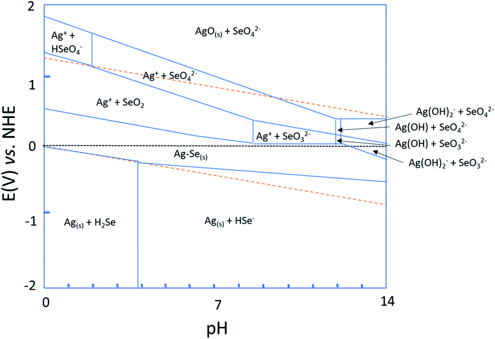 | ||
| Fig. 1 Pourbaix diagram of 50% silver, 50% selenium in water vs. NHE reference electrode at 25 °C. The Ag–Se region corresponds to Ag2Se, although different relative concentrations of Ag/Se will be obtained depending on the pH and the voltage. | ||
To determine whether Ag2Se can be experimentally obtained without any additive added to the solution, as seems to be indicated by the Pourbaix diagram, cyclic voltammetry was performed in an aqueous solution of 5 Mm H2SeO3 + 5 mM AgNO3 + 0.2 M H2SO4 over the OCP (open circuit potential) = 0.468 V to −0.8 V, 0.8 V, to OCP vs. Ag/AgCl (see Fig. 2a). The scan rate was 10 mV s−1 and the electrochemical experiments were carried out at room temperature.
 | ||
| Fig. 2 (a) Cyclic voltammetry of an aqueous solution of 5 Mm H2SeO3 + 5 mM AgNO3 + 0.2 M H2SO4 over the OCP (open circuit potential) = 0.468 V to −0.8 V to 0.8 V vs. Ag/AgCl. Scan rate 10 mV s−1, room temperature. (b) Cyclic voltammetry around the reduction peak of Se2− (5 mM) and Ag+ (5 mM) in 0.2 M H2SO4. | ||
As Fig. 2a shows, there are three reduction peaks and two oxidation peaks in the cyclic voltammetry. The reduction potential located at 0.4 V corresponds to the reduction of Ag+ to Ag. This was confirmed by depositing at that potential and analyzing the resulting deposit. The reduction peak at around 0.1 V is due to the reduction of Ag+ and H2SeO3 to Ag2Se according to reaction (1). And the last reduction peak around −0.6 V corresponds to the reduction of Ag2Se to elemental silver and H2Se anions. This was confirmed by depositing at that potential, where no deposit was obtained after 2 h. Fig. 2b shows the silver selenide reduction peak in detail. Since the purpose of this study is to obtain silver selenide films, the electrodeposition was performed at different reduction potentials located around the silver selenide reduction peak, as shown in Fig. 2b. The electrodeposition time was 2 h for all the grown films.
Compositional, morphological, and structural characterization of silver selenide films
Once the silver selenide films were electrodeposited at different reduction potentials for 2 h, the compositions of such films were analyzed by EDX (see Table 2).| Films | Atomic% Se | Atomic% Ag | Formula | Thickness |
|---|---|---|---|---|
| 0.084 V | 35.1 ± 2 | 63.0 ± 2 | Ag1.8Se | 1043 nm |
| 0.078 V | 32.2 ± 2 | 60.7 ± 2 | Ag1.9Se | 964 nm |
| 0.071 V | 31.5 ± 2 | 68.2 ± 2 | Ag2.2Se | 860 nm |
| 0.044 V | 32.8 ± 2 | 67.0 ± 2 | Ag2.1Se | 1035 nm |
| −0.015 V | 34.7 ± 2 | 64.1 ± 2 | Ag1.9Se | 1054 nm |
The compositions are Ag1.8Se, Ag1.9Se, Ag2.2Se, Ag2.1Se, and Ag1.9Se for 0.084, 0.078, 0.071, 0.044, and −0.015 V, respectively. All the films presented in this study exhibit a composition close to Ag2Se. The thickness of the films is collected in Table 1, showing values between 860 and 1043 nm.
The morphology of silver selenide films was analyzed using FE-SEM images (see Fig. 3). The morphology of the silver selenide films presents large grains for all cases, but depending on the reduction potential applied, the grain size is different. The grain size was in the ranges 80–650 nm, 110–900 nm, 110–640 nm, 140–500 nm, and 140–525 nm for 0.084, 0.078, 0.071, 0.044, and −0.015 V, respectively. Moreover, the small and bright grains correspond to a higher Ag content, as corroborated by EDX measurements. The films which present these grains were grown at 0.084 and −0.015 V.
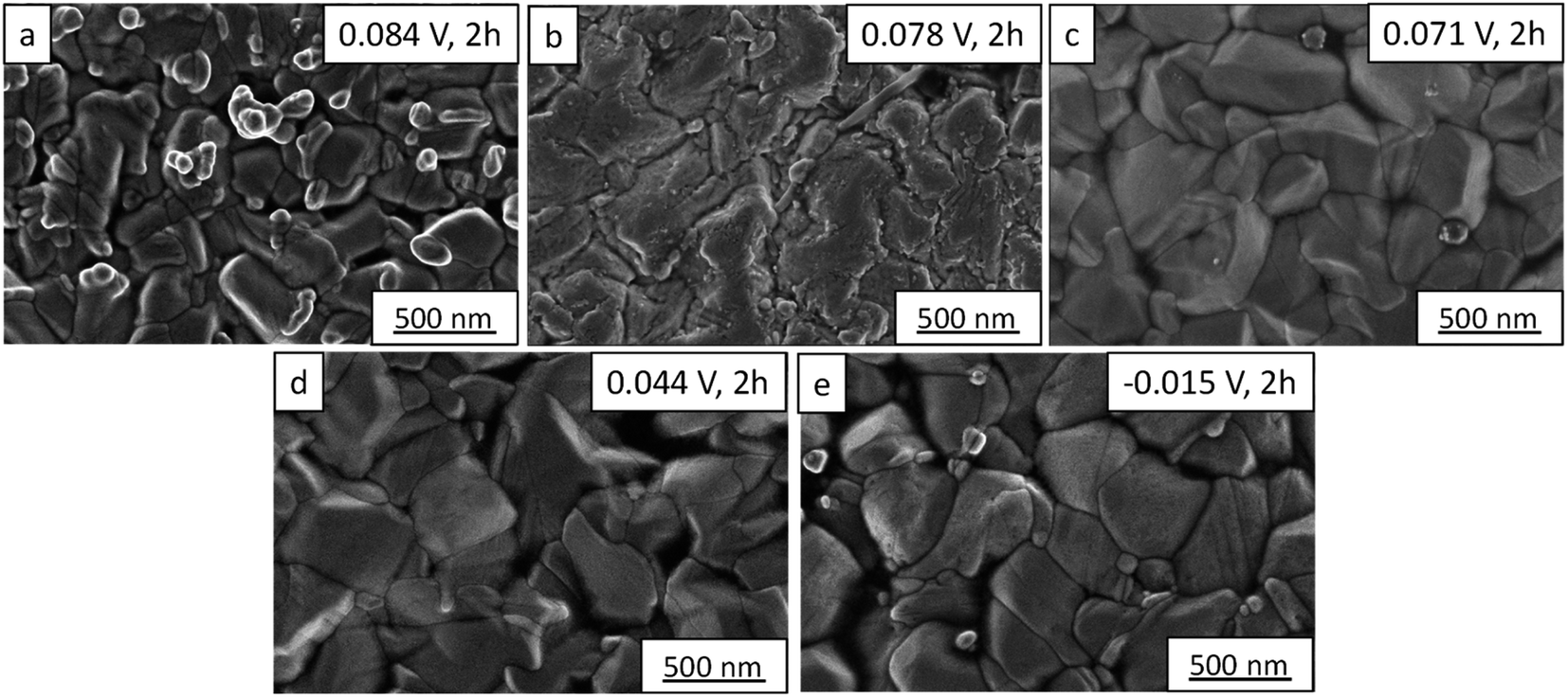 | ||
| Fig. 3 FE-SEM images of silver selenide films grown at different reduction potentials: (a) 0.084 V, (b) 0.078, (c) 0.071, (d) 0.044, and (e) −0.015 V. | ||
In the studies reported in the literature for electrodeposited Ag2Se films,29–32 the morphology observed is very different from that observed in this work, probably due to the electrodeposition solution. In this study, a solution without any additives was applied. The additives normally change the grain size and then the electrical and thermal conductivities. However, silver selenide thin films grown by sputtering exhibit a similar morphology, but with larger grains of 1–2 μm.19
To study the crystallographic structure of the silver selenide films, XRD measurements were performed. Fig. 4 shows the X-ray diffractograms of the films grown at different reduction potentials. Different peaks can be seen, which can be associated with the components of the substrate: Au (JCPDS 040784) and Si (JCPDS 27-1402), along with others that correspond to orthorhombic β-Ag2Se (JCPDS 01-071-2410) with a space group P212121.
 | ||
| Fig. 4 X-ray diffractograms of silver selenide films grown at different reduction potentials. The orthorhombic β-Ag2Se phase seems to be present in all the films (JCPDS: 01-071-2410). | ||
Harris texture analysis48 was performed to obtain the degree of preferred orientation quantitatively. The texture coefficient (TC) and the standard deviation (σ), which indicates the deviation intensity of the experimental XRD from published values of JCPDS, equations can be written as:
 | (2) |
 | (3) |
Thermoelectric properties of silver selenide films and a flexible thermoelectric power generator
The carrier concentration and mobility were obtained for the silver selenide films grown at different reduction potentials (see Table 3). The carrier concentration presents a negative value due to the n-type nature of the semiconductor. A semiconductor is a good thermoelectric material if the material has a carrier concentration in the order of 1019 cm−3;49 in this case, the silver selenide films grown in this study present values of carrier concentration in the order of 1019 cm−3. The mobility is around 2.33 × 10² to 9.65 × 102 cm2 V−1 s−1.| Films | Formula | Carrier concentration (cm−3) | Mobility (cm2 V−1 s−1) | Electrical conductivity (S cm−1) | Seebeck coefficient (μV K−1) | Power factor (μW m−1 K−2) |
|---|---|---|---|---|---|---|
| 0.084 V | Ag1.8Se | −1.1 × 10¹⁹ ± 0.5 × 10¹⁸ | 8.1 × 10² | 1380 ± 69 | −136 ± 14 | 2537 ± 523 |
| 0.078 V | Ag1.9Se | −1.1 × 10¹⁹ ± 0.5 × 10¹⁸ | 8.9 × 10² | 1550 ± 78 | −94 ± 9 | 1376 ± 76 |
| 0.071 V | Ag2.2Se | −2.5 × 10¹⁹ ± 0.1 × 10¹⁹ | 7.5 × 10² | 3010 ± 15 | −107 ± 11 | 3421 ± 705 |
| 0.044 V | Ag2.1Se | −1.9 × 10¹⁹ ± 0.1 × 10¹⁹ | 4.4 × 10² | 1280 ± 69 | −112 ± 11 | 1612 ± 332 |
| −0.015 V | Ag1.9Se | −8.7 × 10¹⁸ ± 0.4 × 10¹⁸ | 9.7 × 10² | 1380 ± 69 | −118 ± 12 | 1916 ± 395 |
The thermoelectric properties, electrical conductivity, Seebeck coefficient, and power factor of selenide films, are shown in Fig. 5 as a function of the reduction potential.
 | ||
| Fig. 5 (a) Electrical conductivity (black circles), (b) Seebeck coefficient (red triangles), and (c) power factor (blue stars) as a function of the reduction potential of silver selenide films at room temperature. Error bars come from the experimental errors of the measurements. | ||
The maximum value of the electrical conductivity, 3010 ± 15 S cm−1, was observed for the film grown at 0.071 V, which has a composition of Ag2.2Se and a thickness of 860 nm, that is, the thinnest film in this study. Moreover, the morphology of this film is the smoothest. The electrical conductivity values are of the same order as those for bulk Ag2Se found in the literature.20–23,26,27 However, for films, the electrical conductivity was found to be lower with values of 750,19 1000,24 and 920 S cm−125 for films grown by sputtering and vacuum-assisted infiltration on nylon substrate. The value of the electrical conductivity obtained in this study is 3 times higher than the highest values measured in films grown by other techniques.
The Seebeck coefficients (see red triangles in Fig. 5) were found to be −136 ± 14, −94 ± 9, −107 ± 11, −112 ± 11, and −118 ± 12 μV K−1 for 0.084, 0.078, 0.071, 0.044, and −0.015 V, respectively. The maximum Seebeck coefficient of −136 ± 14 was observed for the film grown at 0.084 V. The Seebeck coefficient values obtained in this study are similar to the values found in the literature for bulk silver selenide20–23,26 and films.24,25 The maximum value at this magnitude (−180 μV K−1 at RT) found in the literature was obtained in thin films grown by sputtering.19
The power factor is shown by blue stars, presenting a value of 2537 ± 523, 1376 ± 76, 3421 ± 705, 1612 ± 332, and 1916 ± 395 μW m−1 K−2 for 0.084, 0.078, 0.071, 0.044, and −0.015 V, respectively. The maximum value, 3421 ± 705 μW m−1 K−2, is observed for the film grown at 0.071 V, which is again the thinnest film (860 nm) with the composition Ag2.2Se. The maximum power factor reported in the literature was 3520 μW m−1 K−2 at RT for bulk silver selenide bulk material grown using quartz tubes followed by melting,20 this value being similar to the best value obtained in this study. And it was 1.5 times higher than the values for silver selenide films.19,24,25
Regarding the thermal conductivity of the film grown at 0.071 V, it is 0.56 ± 0.06 W m−1 K−1. This thermal conductivity value is a bit lower than the values found in the literature: 0.64 and 1.5 W m−1 K−1, for thin films19 and bulk material,21 respectively. The values of thermal conductivity are similar to the values obtained in other films, taking into account the measurement error, but are much lower than in bulk. This can be explained by the small crystallite size observed in our film, which is in the range of 80–190 nm according to the XRD calculations.
It is important to note that this material can only be used for thermoelectric devices working at room temperature. The presence of silver mobile ions has been observed previously at temperatures higher than 125 °C.19,50
Finally, to study the performance of the electrodeposited Ag2.2Se film as a flexible thermoelectric power generator, Ag2.2Se films were grown on a Kapton substrate to serve as n-type legs. For such a purpose, the electrodeposition conditions were optimized at the reduction potential which presents the highest thermoelectric properties and compact films were obtained. This thermoelectric power generator is composed of five single legs of silver selenide film (see Fig. 6). The legs were interconnected by a gold film deposited by e-beam evaporation using a shadow mask.
 | ||
| Fig. 6 Photograph of the flexible unileg thermoelectric power generator device composed of five electrodeposited silver selenide films connected by e-beam evaporated gold films. | ||
The maximum powers for the flexible thermoelectric power generator formed of five silver selenide unilegs were approximately 14.7, 29.4, and 37 μW under temperature differences of 10, 15, and 19 K, respectively. Therefore, maximum power densities of 55.1, 110.1, and 138.6 mW m−2 under temperature differences of 10, 15, and 19 K, respectively, were achieved. In our case, a temperature difference of 10–20 K was considered because it is a realistic value for wearable applications. By comparing these results with previous thermoelectric devices based on Ag2Se film fabricated by a screen printing technique in which 13 thermocouples were measured at 30 K of temperature difference,51 it can be seen that our results are very promising. To compare that value with our results, we divided the maximum power density reported by the total number of pairs of legs, obtaining ∼5 mW m−251versus ∼138.6 mW m−2, in our case. This is a very interesting result, even more so, taking into account that a third of the temperature gradient was used in our study.
Conclusions
In conclusion, silver selenide films were grown by electrodeposition at different reduction potentials. To obtain these films, the Pourbaix diagram of silver selenide was firstly calculated to identify an adequate pH and reduction potential for the electrodeposition of stable silver selenide without the need for chelating agents. The compositional, morphological, and structural characterization of the silver selenide thin films were optimized to find a denser planar film when it was deposited at 0.071 V. The thermoelectric properties of these films were measured at room temperature. The maximum power factor was measured for the films grown at 0.071 V with a value of 3421 ± 705 μW m−1 K−2 and a thermal conductivity of 0.56 ± 0.06 W m−1 K−1. A flexible thermoelectric power generator of five silver selenide films interconnected by gold was performed on Kapton substrate, and a maximum output power of approximately 4.6 μW at a temperature difference of 19 K and a maximum power density of 138.6 mW m−2 were observed.Conflicts of interest
The authors declare no competing financial interests.Acknowledgements
The authors would like to acknowledge financial support from MAT2017-86450-C4-3-R and CSIC PIF 2D-MESES. Cristina V. Manzano would like to acknowledge funding from “Atracción de Talento Investigador” de la Comunidad de Madrid, contract 2019-T1/IND-13541. We acknowledge support of the publication fee by the CSIC Open Access Publication Support Initiative through its Unit of Information Resources for Research (URICI). We acknowledge the service from the MiNa Laboratory at IMN, and funding from CM (project SpaceTec, S2013/ICE2822), MINECO (project CSIC13-4E-1794), and the EU (FEDER, FSE).References
- Y. Wang, L. Yang, X.-L. Shi, X. Shi, L. Chen, M. S. Dargusch, J. Zou and Z.-G. Chen, Adv. Mater., 2019, 31, 1807916 CrossRef PubMed.
- J.-H. Bahk, H. Fang, K. Yazawa and A. Shakouri, J. Mater. Chem. C, 2015, 3, 10362–10374 RSC.
- A. Nozariasbmarz, H. Collins, K. Dsouza, M. H. Polash, M. Hosseini, M. Hyland, J. Liu, A. Malhotra, F. M. Ortiz, F. Mohaddes, V. P. Ramesh, Y. Sargolzaeiaval, N. Snouwaert, M. C. Özturk and D. Vashaee, Appl. Energy, 2020, 258, 114069 CrossRef.
- R. Freer and A. V. Powell, J. Mater. Chem. C, 2020, 8, 441–463 RSC.
- A. R. M. Siddique, S. Mahmud and B. V. Heyst, Renewable Sustainable Energy Rev., 2017, 73, 730–744 CrossRef.
- M. Martín-González, O. Caballero-Calero and P. Díaz-Chao, Renewable Sustainable Energy Rev., 2013, 24, 288–305 CrossRef.
- M. Muñoz Rojo, B. Abad, C. V. Manzano, P. Torres, X. Cartoixà, F. X. Alvarez and M. Martín Gonzalez, Nanoscale, 2017, 9, 6741–6747 RSC.
- M. Muñoz Rojo, Y. Zhang, C. V. Manzano, R. Alvaro, J. Gooth, M. Salmeron and M. Martin-Gonzalez, Sci. Rep., 2016, 6, 19014–19018 CrossRef.
- A. I. Hochbaum, R. Chen, R. D. Delgado, W. Liang, E. C. Garnett, M. Najarian, A. Majumdar and P. Yang, Nature, 2008, 451, 163–167 CrossRef CAS.
- C. V. Manzano, B. Abad, M. Muñoz Rojo, Y. R. Koh, S. L. Hodson, A. M. Lopez Martinez, X. Xu, A. Shakouri, T. D. Sands, T. Borca-Tasciuc and M. Martin-Gonzalez, Sci. Rep., 2016, 6, 19129 CrossRef CAS PubMed.
- C. V. Manzano and M. Martín-González, Front. Chem., 2019, 7, 516 CrossRef CAS PubMed.
- G. Tan, F. Shi, S. Hao, L.-D. Zhao, H. Chi, X. Zhang, C. Uher, C. Wolverton, V. P. Dravid and M. G. Kanatzidis, Nat. Commun., 2016, 7, 12167 CrossRef CAS PubMed.
- T.-R. Wei, C.-F. Wu, F. Li and J.-F. Li, J. Materiomics, 2018, 4, 304–320 CrossRef.
- D. Beretta, N. Neophytou, J. M. Hodges, M. G. Kanatzidis, D. Narducci, M. Martin-Gonzalez, M. Beekman, B. Balke, G. Cerretti, W. Tremel, A. Zevalkink, A. I. Hofmann, C. Müller, B. Dörling, M. Campoy-Quiles and M. Caironi, Mater. Sci. Eng., R, 2019, 138, 100501 CrossRef.
- U.S. Geological Survey, Mineral Commodity Summaries 2020, Reston, VA, 2020 Search PubMed.
- L.-D. Zhao, S.-H. Lo, Y. Zhang, H. Sun, G. Tan, C. Uher, C. Wolverton, V. P. Dravid and M. G. Kanatzidis, Nature, 2014, 508, 373 CrossRef CAS.
- C. Chang, G. Tan, J. He, M. G. Kanatzidis and L.-D. Zhao, Chem. Mater., 2018, 30, 7355–7367 CrossRef CAS.
- H. Liu, X. Shi, F. Xu, L. Zhang, W. Zhang, L. Chen, Q. Li, C. Uher, T. Day and G. J. Snyder, Nat. Mater., 2012, 11, 422–425 CrossRef CAS PubMed.
- J. A. Perez-Taborda, O. Caballero-Calero, L. Vera-Londono, F. Briones and M. Martin-Gonzalez, Adv. Energy Mater., 2018, 8, 1702024 CrossRef.
- M. Ferhat and J. Nagao, J. Appl. Phys., 2000, 88, 813–816 CrossRef CAS.
- T. Day, F. Drymiotis, T. Zhang, D. Rhodes, X. Shi, L. Chen and G. J. Snyder, J. Mater. Chem. C, 2013, 1, 7568–7573 RSC.
- W. Mi, P. Qiu, T. Zhang, Y. Lv, X. Shi and L. Chen, Appl. Phys. Lett., 2014, 104, 133903 CrossRef.
- D. Yang, X. Su, F. Meng, S. Wang, Y. Yan, J. Yang, J. He, Q. Zhang, C. Uher, M. G. Kanatzidis and X. Tang, J. Mater. Chem. A, 2017, 5, 23243–23251 RSC.
- Y. Ding, Y. Qiu, K. Cai, Q. Yao, S. Chen, L. Chen and J. He, Nat. Commun., 2019, 10, 841 CrossRef PubMed.
- C. Jiang, Y. Ding, K. Cai, L. Tong, Y. Lu, W. Zhao and P. Wei, ACS Appl. Mater. Interfaces, 2020, 12, 9646–9655 CrossRef CAS.
- H. Wang, W. Chu, D. Wang, W. Mao, W. Pan, Y. Guo, Y. Xiong and H. Jin, J. Electron. Mater., 2011, 40, 624–628 CrossRef CAS.
- C. Lee, Y.-H. Park and H. Hashimoto, J. Appl. Phys., 2007, 101, 024920 CrossRef.
- J. Pei, G. Chen, D. Jia, R. Jin, H. Xu and D. Chen, New J. Chem., 2013, 37, 323–328 RSC.
- R. Chen, D. Xu, G. Guo and Y. Tang, J. Mater. Chem., 2002, 12, 1437–1441 RSC.
- S. J. Pawar, P. P. Chikode, V. J. Fulari and M. B. Dongare, Mater. Sci. Eng. B, 2007, 137, 232–236 CrossRef CAS.
- B. H. An, H. M. Ji, J. H. Wu, M. K. Cho, K. Y. Yang, H. Lee and Y. K. Kim, Curr. Appl. Phys., 2009, 9, 1338–1340 CrossRef.
- U. Chougale, S.-H. Han, M. Rath and V. Fulari, Mater. Phys. Mech., 2013, 17, 47–58 CAS.
- R. Chen, D. Xu, G. Guo and L. Gui, Electrochem. Commun., 2003, 5, 579–583 CrossRef CAS.
- L. Genovese, C. Cocchiara, S. Piazza, C. Sunseri and R. Inguanta, Mater. Res. Bull., 2017, 86, 10–18 CrossRef CAS.
- C. V. Manzano, A. A. Rojas, M. Decepida, B. Abad, Y. Feliz, O. Caballero-Calero, D. A. Borca-Tasciuc and M. Martin-Gonzalez, J. Solid State Electrochem., 2013, 17, 2071–2078 CrossRef CAS.
- O. Caballero-Calero, P. Díaz-Chao, B. Abad, C. V. Manzano, M. D. Ynsa, J. J. Romero, M. M. Rojo and M. S. Martín-González, Electrochim. Acta, 2014, 123, 117–126 CrossRef CAS.
- H. Hu, X. Wang and X. Xu, J. Appl. Phys., 1999, 86, 3953–3958 CrossRef CAS.
- B. Abad, J. Maiz and M. Martin-Gonzalez, J. Phys. Chem. C, 2016, 120, 5361–5370 CrossRef CAS.
- B. Abad, M. Rull-Bravo, S. L. Hodson, X. Xu and M. Martin-Gonzalez, Electrochim. Acta, 2015, 169, 37–45 CrossRef CAS.
- J. Maiz, M. Rojo, B. Abad, A. Wilson, A. Nogales, D.-A. Borca-Tasciuc, T. Borca-Tasciuc and M. Martín-González, RSC Adv., 2015, 5, 66687 RSC.
- J. A. P. Taborda, J. J. Romero, B. Abad, M. Muñoz-Rojo, A. Mello, F. Briones and M. S. M. Gonzalez, Nanotechnology, 2016, 27, 175401 CrossRef PubMed.
- B. Abad, J. Maiz, A. Ruiz-Clavijo, O. Caballero-Calero and M. Martin-Gonzalez, Sci. Rep., 2016, 6, 38595 CrossRef CAS PubMed.
- C. V. Manzano, B. Abad and M. Martín-González, J. Electrochem. Soc., 2018, 165, D768–D773 CrossRef CAS.
- K. A. Persson, B. Waldwick, P. Lazic and G. Ceder, Phys. Rev. B: Condens. Matter Mater. Phys., 2012, 85, 235438 CrossRef.
- W. T. Thompson, M. H. Kaye, C. W. Bale and A. D. Pelton, Uhlig's Corrosion Handbook, 2011, pp. 103–109 Search PubMed.
- M. S. Martín-González, A. L. Prieto, R. Gronsky, T. Sands and A. M. Stacy, J. Electrochem. Soc., 2002, 149, C546–C554 CrossRef.
- J. Kretzschmar, N. Jordan, E. Brendler, S. Tsushima, C. Franzen, H. Foerstendorf, M. Stockmann, K. Heim and V. Brendler, Dalton Trans., 2015, 44, 10508–10515 RSC.
- G. B. Harris, Philos. Mag., 1952, 43, 113–123 Search PubMed.
- M. Bittner, N. Kanas, R. Hinterding, F. Steinbach, J. Räthel, M. Schrade, K. Wiik, M.-A. Einarsrud and A. Feldhoff, J. Power Sources, 2019, 410–411, 143–151 CrossRef CAS.
- M. Schwarz, A. Mews and A. Dorn, Nanoscale, 2021, 13, 8017–8023 RSC.
- M. M. Mallick, A. G. Rösch, L. Franke, S. Ahmed, A. Gall, H. Geßwein, J. Aghassi and U. Lemmer, ACS Appl. Mater. Interfaces, 2020, 12, 19655–19663 CrossRef CAS.
Footnote |
| † Electronic supplementary information (ESI) available. See DOI: 10.1039/d1se01061a |
| This journal is © The Royal Society of Chemistry 2021 |