MXenes: promising donor and acceptor materials for high-efficiency heterostructure solar cells†
Received
25th September 2020
, Accepted 22nd October 2020
First published on 22nd October 2020
Abstract
Constructing heterostructure solar cells using donor and acceptor semiconductors has attracted global interest owing to their high power conversion efficiency. In this paper, based on density functional theory calculations, we comprehensively evaluated 64 two-dimensional transition metal carbides (MXenes) to explore them as appropriate semiconductors for solar cells by material screening. The results highlight that Zr2CO2 (Hf2CO2) and Ti2CO2 are promising donor and acceptor materials, respectively. Interestingly, the heterostructures have a moderate band gap of 1.22 eV and exhibit a noticeable absorbance coefficient of 105 cm−1 in the visible light region. Moreover, the type-II nature of the heterostructures could induce effective electron–hole separation. Furthermore, the photocurrents of Ti2CO2/Zr2CO2 and Ti2CO2/Hf2CO2 heterostructure solar cell devices are competitive with those of silicon devices. In particular, Ti2CO2/Zr2CO2 and Ti2CO2/Hf2CO2 heterostructure solar cells deliver a very high power conversion efficiency of 22.74% and 19.56%, respectively. Our present study paves the way for facilitating the potential application of MXenes as photovoltaic materials.
1. Introduction
Solar cells converting sunlight directly into electricity provide a new approach for the sustainable application of green and clean solar energy. Different two-dimensional (2D) semiconductors combining van der Waals (vdW) via the vdW interaction have been reported as an efficient method for designing high-quality solar cells.1–6 A primary requirement for a high-quality heterostructure solar cell is that the band gaps of both donor and acceptor materials should be in the range of roughly 1.2–1.6 eV.1 The migration of free electron–hole pairs in solar cells plays a vital role in the efficiency performance. Hence, carrier transfer is also a critical factor that cannot be ignored in constructing heterostructure solar cell devices. However, few 2D materials can meet all the requirements for heterostructure solar cells, and the selection of appropriate donor and acceptor materials for high-efficiency solar cells is of great importance and urgency.2
MXenes7–14 are 2D transition metal carbides/nitrides produced from their corresponding MAX phases, where M represents early transition metals, A stands for group IIIA or IVA elements and X corresponds to a C or N atom.9 MXenes have garnered increasing interest because of their various potential applications such as photocatalytic water splitting,15–17 Li-ion and Na-ion battery anodes,18,19 metal-ion capacitors,20 heavy metal removal21etc. In previous ingenious studies,3,22 both 2D TiNX (X = F, Cl, and Br) and edge-modified phosphorene have been demonstrated as suitable semiconductors for forming heterostructure solar cells. Coincidently, the outer layers of MXenes are saturated with F, O, and/or OH groups when exfoliating from their bulk MAX phases.23,24 Motivated by this, we wonder if MXenes are endowed with an outstanding feature for the design of 2D heterostructure solar cells.
Considering the large number of compounds in the MXene family, we employed a computational method instead of the traditional trial-and-error approach to extensively investigate the optoelectronic properties of MXenes. In this work, by first-principles calculations, we studied the photoelectronic properties of 64 MXenes for seeking feasible photovoltaic materials. Accordingly, Zr2CO2 (Hf2CO2) and Ti2CO2 were chosen as donor and acceptor materials to form heterostructure solar cells, respectively. We then constructed Ti2CO2/Zr2CO2 and Ti2CO2/Hf2CO2 heterostructures to explore their potential application as photovoltaic devices. The high stability, ideal band gaps, and highly effective separation of photo-induced free carriers of Ti2CO2/Zr2CO2 and Ti2CO2/Hf2CO2 heterostructures have been confirmed, making them promising candidates for high-quality solar cell devices. Significantly, the estimated maximum power conversion efficiency (PCE) of Ti2CO2/Zr2CO2 and Ti2CO2/Hf2CO2 heterostructures can be as high as 22.74% and 19.56%, respectively, which are absolutely competitive with other existing 2D heterostructures.
2. Theoretical methods
Our calculations were based on density functional theory (DFT) as implemented in the Vienna ab initio simulation package (VASP).25,26 For the exchange-correlation functional, the projector augmented-wave (PAW)27 of generalized gradient approximation (GGA) with Perdew–Burke–Ernzerhof (PBE) formalism28 was used. The DFT-D3 (ref. 29) method was employed due to its good description in long-range vdW interactions. Considering the correlation effects of d electrons of the Ti atom, the GGA+U26,30,31 approach was used for Ti-related MXenes, of which the correction parameter U of Ti was set to 3 eV by referring to previous studies.32–34 The Heyd–Scuseria–Ernzerhof (HSE06)35 hybrid density functional combined with DFT-D3 was used to calculate the band gaps. To include the excitonic effects, time-dependent Hartree–Fock calculations (TDHF)36 were adopted to calculate optical properties. The PHONOPY code was used to obtain the phonon dispersion curves37,38 using a 3 × 3 × 1 supercell with a k-point mesh of 3 × 3 × 1. The Born–Oppenheimer ab initio molecular dynamics (AIMD) simulations were adopted to assess the stability of MXenes from 300 K to 2400 K for 9 ps. A 4 × 4 × 1 supercell has been constructed for AIMD calculations. Some additional calculation details for formation and binding energy, carrier mobility, and device photocurrent by using a QuantumWise Atomistix ToolKit (QuantumATK) Q2019.12 package39 are summarized in the ESI.†
3. Results and discussion
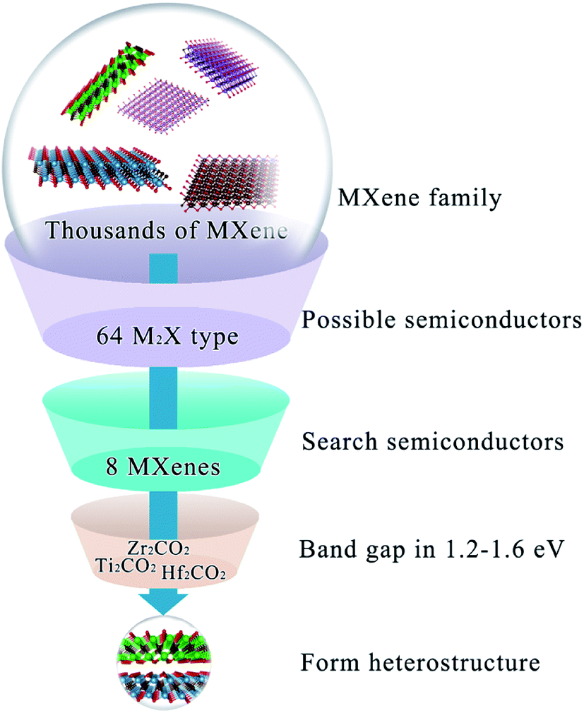
So far, semiconducting MXenes have been only found in M2X-type ones10 where M stands for early transition metals listed in Fig. S1a† and X represents C or N. Therefore, to extensively investigate the possibility of MXenes as the donor and acceptor for solar cells, our calculations considered experimental and theoretical M2X-type MXenes referred to in a review article published very recently14 in Fig. S1b.† MXenes exhibit metal to semiconductor transformation modulated by terminal functional groups;23,24 hence both pristine and functionalized MXenes (O, OH or F groups) were explored in this work (including 64 MXenes in total). Initial screening for MXenes as promising photovoltaic materials is dependent on their electronic structures; hence the band structure of semiconducting or semi-metallic MXenes by the HSE06 method ispresented in Fig. S2.† The results suggest that Mo2CO2 and W2CO2 show a gapless semi-metallic electronic structure feature, while Sc2CF2, Sc2CO2, Sc2C(OH)2, Ti2CO2, Zr2CO2, Hf2CO2, Mo2CF2 and W2CF2 are semiconductors having band gaps from 0.51 to 2.96 eV. However, the band gaps of Sc2CF2 (1.86 eV), Sc2CO2 (2.96 eV), Sc2C(OH)2 (0.77 eV), Mo2CF2 (0.88 eV), and W2CF2 (0.51 eV) are either too large or too small to meet the primary requirement for active materials with a band gap in roughly 1.2–1.6 eV. Therefore, we focused on Ti2CO2, Zr2CO2 and Hf2CO2 as donor or acceptor materials to form heterostructure solar cells in the next step. The overall screening process is summed up in Fig. 1.
 |
| | Fig. 1 The overall screening process of candidate MXenes for heterostructure solar cells. | |
It is worth noting that the matched band alignment of the donor and acceptor is a crucial requirement to the formation of a type-II heterostructure solar cell. In a type-II heterostructure, as displayed in the inset of Fig. S3,† both the conduction band minimum (CBM) and valence band maximum (VBM) of semiconductor A must be lower than those of semiconductor B. Since electrons and holes gain energy by moving down and up respectively, after the contact between conductor A and B, photo-excited electrons can transfer from the CBM (B) to CBM (A), and vice versa and the holes can be transferred from the VBM (A) to VBM (B) simultaneously.40 Following this principle, we illustrated the electronic band alignment of MXenes referring to the vacuum level in Fig. S3.† It is clear that both Zr2CO2 and Hf2CO2 are potential donor semiconductors to form heterostructure solar cells with Ti2CO2 as the acceptor material for designing type-II solar cells.
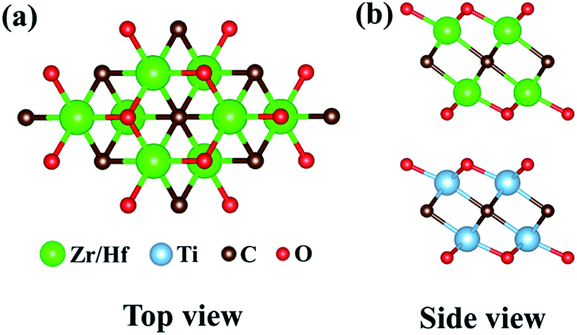
The optimized lattice constants of Ti2CO2, Zr2CO2, and Hf2CO2 are 3.065, 3.292, and 3.25 Å, respectively, agreeing well with previous studies.15,41 Herein, the lattice mismatch between Zr2CO2 (Hf2CO2) and Ti2CO2 is 7.4% (6.0%), which is larger than that for well-known heterostructures.7,42,43 However, the creation of Ti2CO2/Zr2CO2 (Ti2CO2/Hf2CO2) is still expected because MXenes can sustain very large tensile strains.44 For the combined heterostructures, six selective stacking patterns with six special rotation angles between the adjacent layers were explored, as shown in Fig. S4.† The rotation angles of Zr2CO2 (Hf2CO2) with respect to Ti2CO2 are 0°, 60°, 120°, 180°, 240° and 300°, respectively. All the configurations were geometry optimized for achieving stable atomic systems. Table S1† lists the difference of the calculated energy between the six configurations, the interlayer distances between Ti2CO2 and Zr2CO2 (Hf2CO2) layers, lattice constant a (Å) and bond lengths for monolayers and heterostructures. The energy difference ΔE can be defined as:
where
Ei is the total energy of each configuration and
E0 is the total energy of the most stable one. As is seen in Table S1,
† the bond length changes less, exhibiting small atomic rearrangements. Moreover, the calculated total energies of different stackings are proportional to the interlayer distances, so the most stable structures are configuration (a) possessing the smallest interlayer distance, as illustrated in
Fig. 2. This is because the components in this stacking are embedded in each other slightly, which is beneficial for maintaining the structural stability. Such a phenomenon is consistent with the fact that configuration (a) also exhibits the lowest total energy compared with other bilayer stacking configurations in Ti
2CO
2, Zr
2CO
2, and Hf
2CO
2 as proved by previous studies.
16,33 On the other hand, the estimated interface formation energies according to eqn (S1) of the ESI
† of Ti
2CO
2/Zr
2CO
2 and Ti
2CO
2/Hf
2CO
2 heterostructures are 163 meV and 30 meV, respectively. These small positive values indicate that the formation of these two heterostructures is energetically favorable. In addition, the binding energy between Ti
2CO
2 and Zr
2CO
2 (Hf
2CO
2) layers in the heterostructures according to eqn (S2) of the ESI
† is calculated to be 39.05 (36.43) meV Å
−2, similar to the vdW binding energy calculated by the DFT method. Thus, the Ti
2CO
2/Zr
2CO
2 and Ti
2CO
2/Hf
2CO
2 heterostructures belong to vdW heterostructures.
45,46
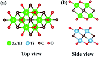 |
| | Fig. 2 (a) Top and (b) side views of Ti2CO2/Zr2CO2 and Ti2CO2/Hf2CO2 heterostructures with the most stable configuration. | |
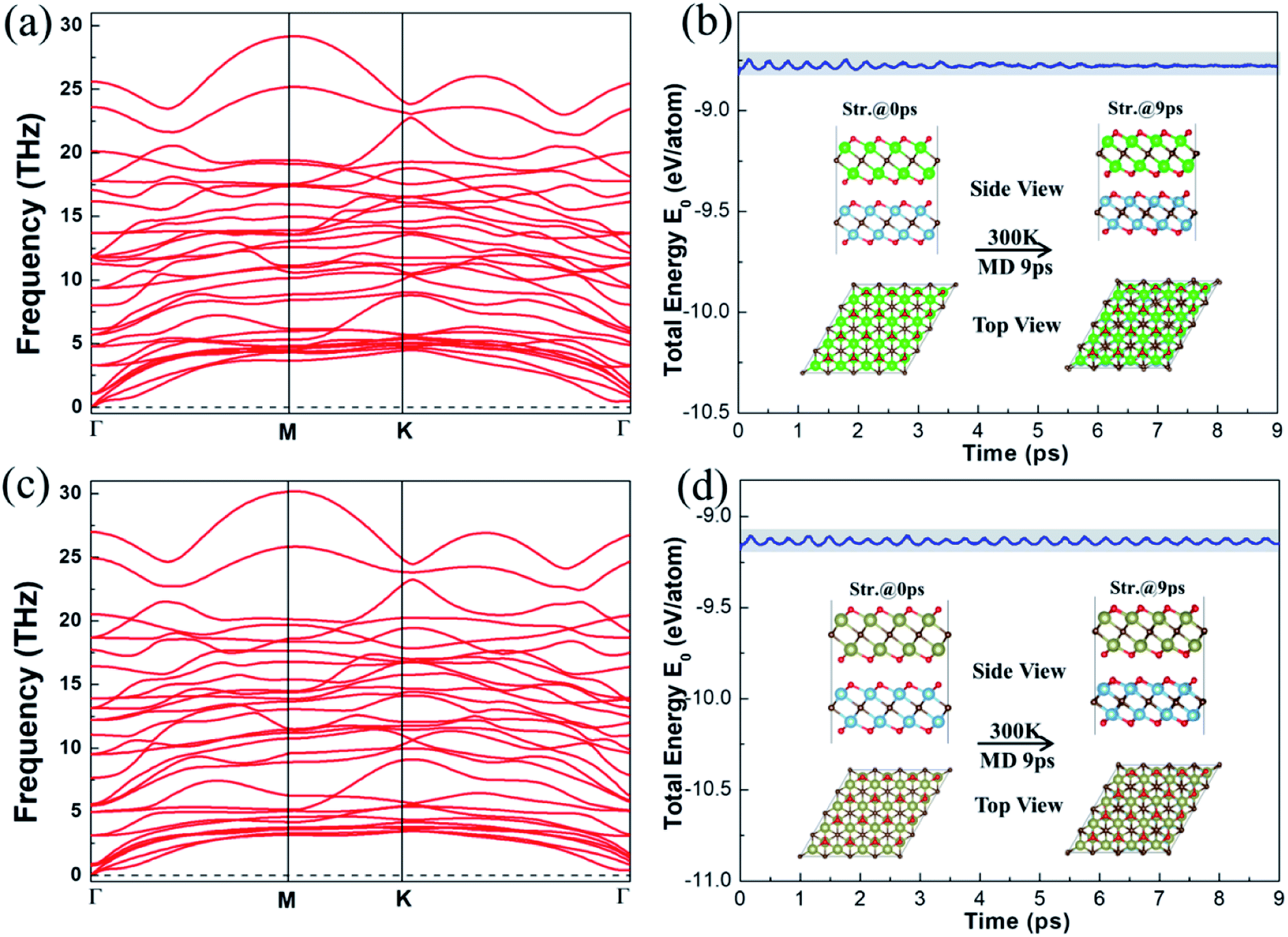
We then performed phonon and AIMD calculations to assess the stability of the vdW heterostructures, respectively. Fig. 3 displays the dispersion curves and energy evolution at 300 K for 9 ps of the vdW heterostructures. Clearly, negative frequency has not been found in Fig. 3a and c, indicating that the Ti2CO2/Zr2CO2 and Ti2CO2/Hf2CO2 vdW heterostructures are lattice dynamically stable. As shown in Fig. 3b and d, it is obvious that the changes of the total energy are very small during the simulations, implying that the Ti2CO2/Zr2CO2 and Ti2CO2/Hf2CO2 vdW heterostructures are thermally stable at room temperature. Furthermore, from the results of annealing the Ti2CO2/Zr2CO2 and Ti2CO2/Hf2CO2 vdW heterostructures at higher temperature in Fig. S5 and S6,† respectively, we can conclude that the atoms in the vdW heterostructures are well maintained around their equilibrium positions with slight vibration until the temperature reaches 2100 K. The results suggest that the Ti2CO2/Zr2CO2 and Ti2CO2/Hf2CO2 vdW heterostructures can hold steady at high temperature up to 2100 K. Hence the stability of the vdW heterostructures has been attested, and coincides with that of our previous energetically favorable analysis.
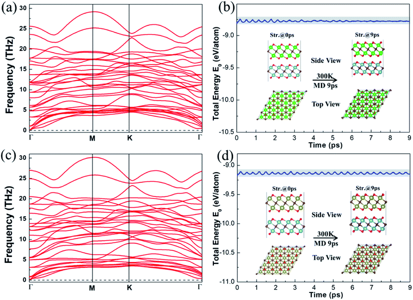 |
| | Fig. 3 Phonon dispersion curves of (a) Ti2CO2/Zr2CO2 and (c) Ti2CO2/Hf2CO2 heterostructures. Total energy changes and snapshots from AIMD calculations at 0 and 9 ps of (b) Ti2CO2/Zr2CO2 and (d) Ti2CO2/Hf2CO2 heterostructures, respectively. | |
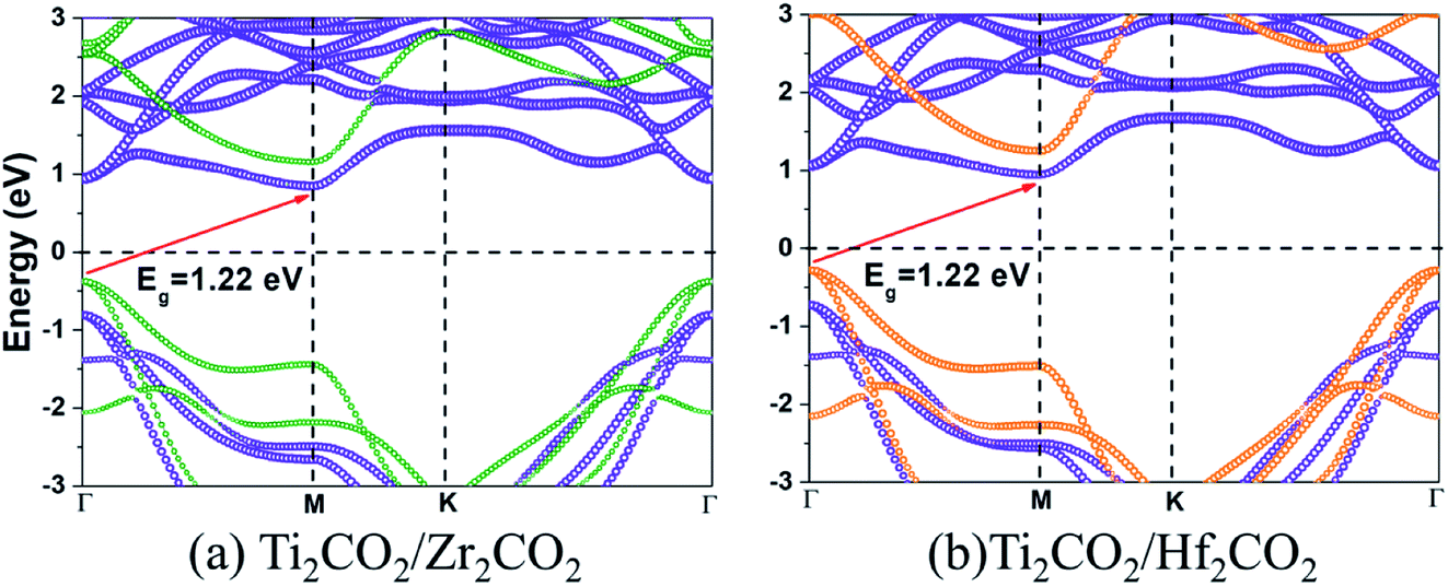
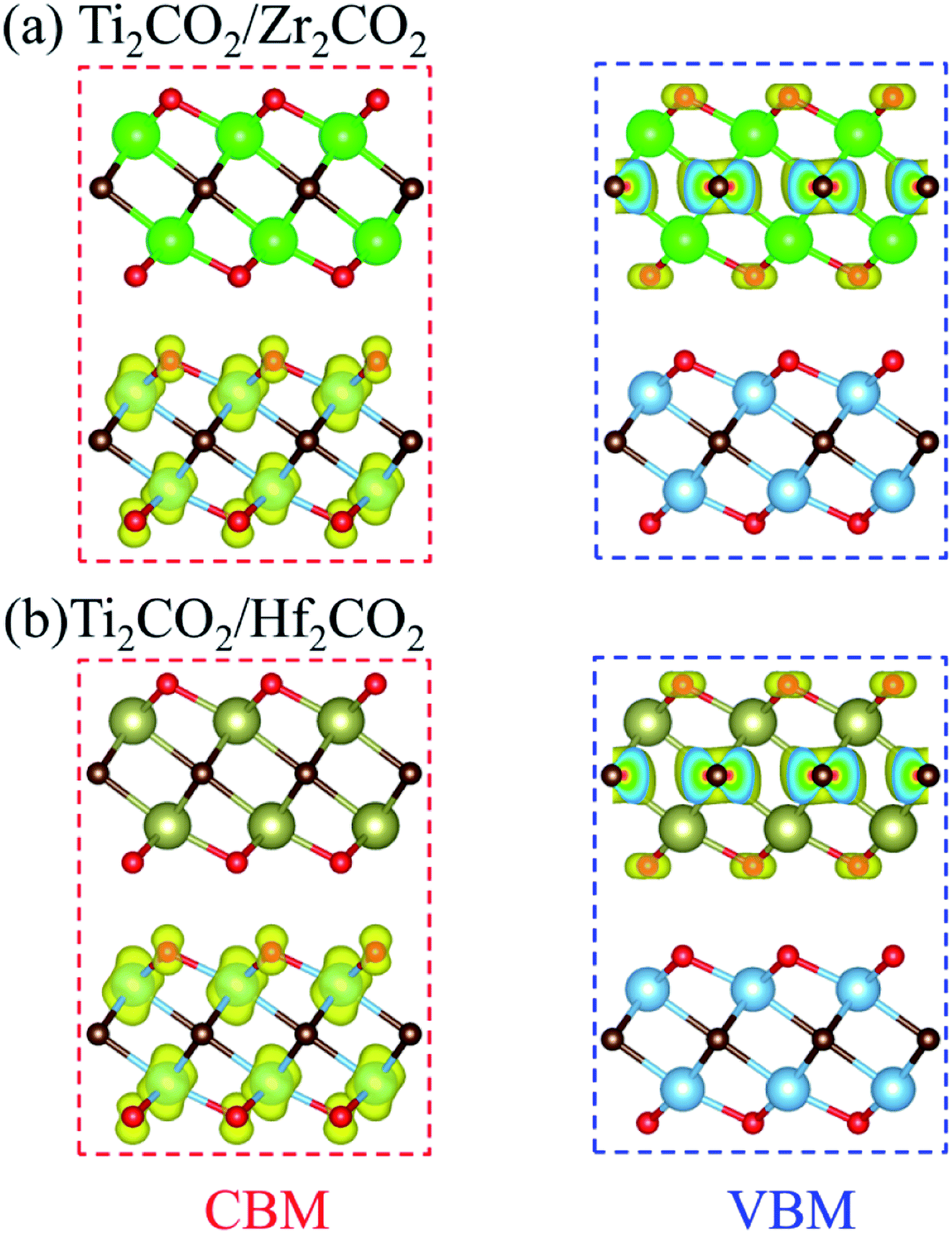
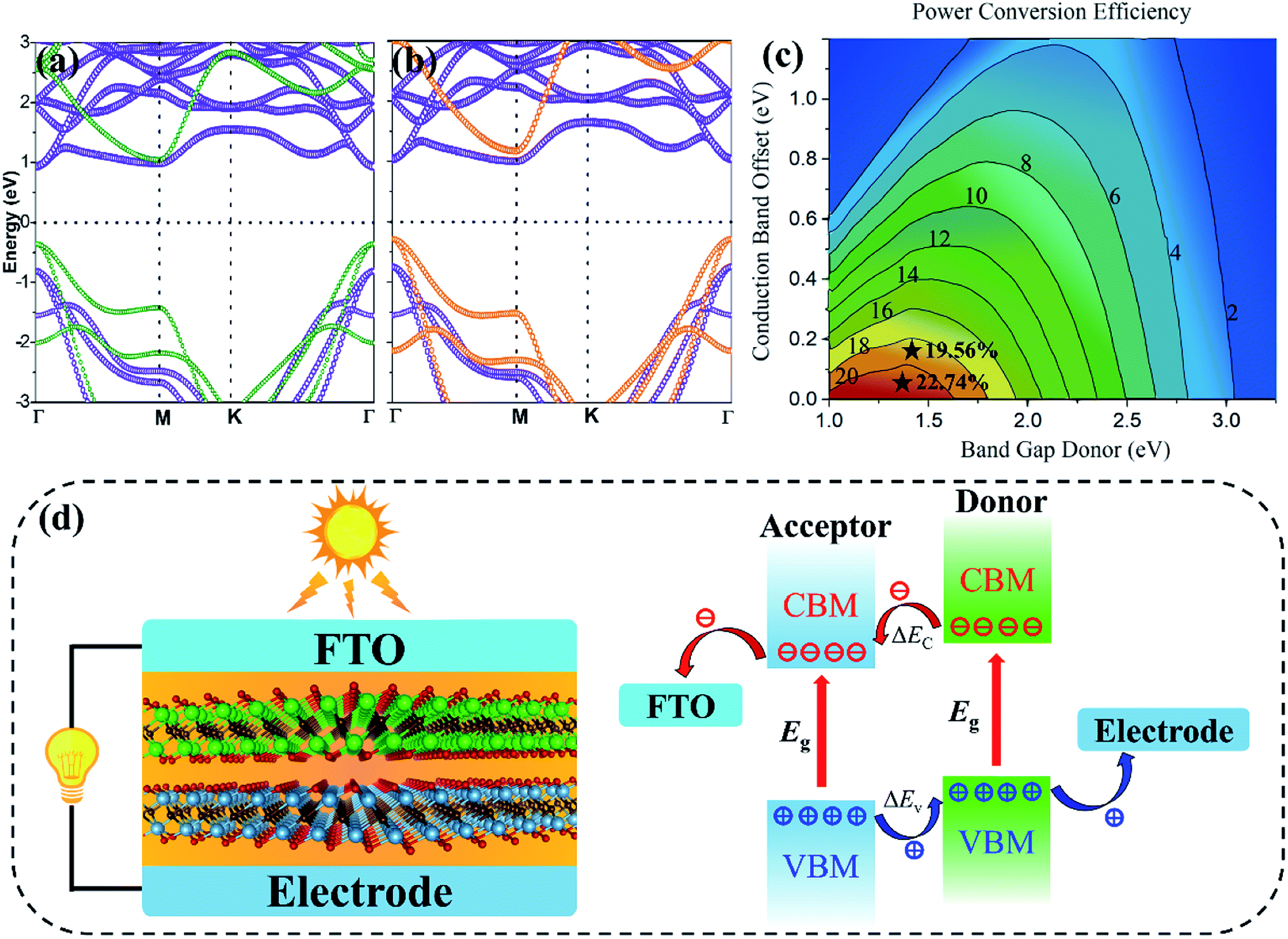
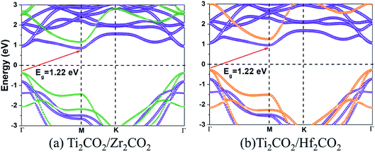
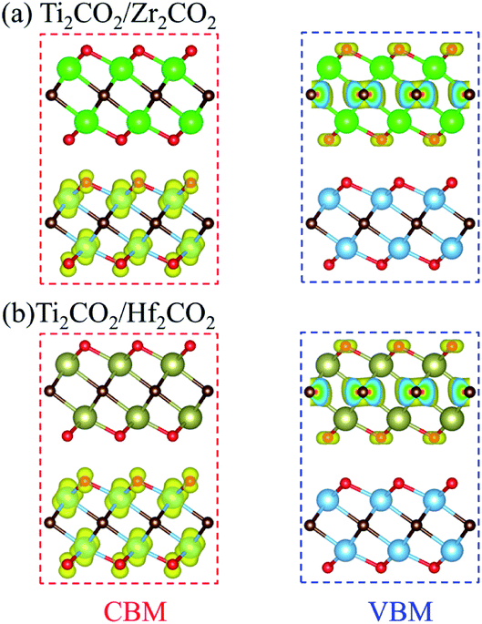
The band gaps of both Ti2CO2/Zr2CO2 and Ti2CO2/Hf2CO2 vdW heterostructures calculated by the HSE06 method are 1.22 eV, similar to the experimental silicon gap. It is worth noting that the band structure characteristics of monolayers have passed to the vdW heterostructures because of the weak vdW interactions. As seen in Fig. 4, both Ti2CO2/Zr2CO2 and Ti2CO2/Hf2CO2 vdW heterostructures show an indirect band gap feature, due to the CBM and VBM at the M and Γ points, respectively. Nevertheless, the energy difference between the indirect and direct band gap is very small (less than 90 meV). Such a small difference might be advantageous for carrier lifetimes in potential perovskites as the requirement of a phonon in an indirect band gap can slow down the recombination rate of photo-induced electrons and holes.47 On the other hand, the small indirect to direct band gap difference does not have a big impact on the optical absorption.48,49 Moreover, the CBM of the vdW heterostructure is entirely dominated by the Ti2CO2 layer, while the VBM is completely occupied by the Zr2CO2 (Hf2CO2) layer, showing a staggered type-II gap feature.50 We then illustrated the band-decomposed charge density in Fig. 5 for a deep understanding of the effect of the constituent layer in the vdW heterostructures. As can be seen, for both vdW heterostructures, the CBM is occupied by d electrons of the Ti atom and p orbitals of the O atom from the Ti2CO2 layer, and the VBM is occupied by the p states of the C atom and O atom from the Zr2CO2 (Hf2CO2) layer. Therefore, it can be concluded that the Ti2CO2/Zr2CO2 and Ti2CO2/Hf2CO2 vdW heterostructures are typical type-II heterostructures. Thus, the photo-excited electrons and holes transfer and gather in different layers as mentioned before, which is beneficial for photoenergy detection and harvesting.7,42
 |
| | Fig. 4 The HSE06 band structures for (a) Ti2CO2/Zr2CO2 and (b) Ti2CO2/Hf2CO2 heterostructures. The size of violet, olive, and orange circles indicated the projected weight of contribution from Ti2CO2, Zr2CO2, and Hf2CO2, respectively. | |
 |
| | Fig. 5 Band-decomposed charge density of the CBM and VBM for (a) Ti2CO2/Zr2CO2 and (b) Ti2CO2/Hf2CO2 heterostructures. | |
We have further calculated the carrier mobility of the Ti2CO2/Zr2CO2 and Ti2CO2/Hf2CO2 vdW heterostructures according to Fig. S7 and S8,† respectively. Taking the Ti2CO2/Zr2CO2 vdW heterostructure as an example, the orthorhombic lattice used in the method is displayed in Fig. S7a.† The calculated band structure is presented in Fig. S7b,† where the band structure characteristics of the CBM and VBM indicate the effective mass of electrons and holes, respectively. Fig. S7c and d† respectively display the change of the total energy and band alignment of the Ti2CO2/Zr2CO2 vdW heterostructure with respect to the applied strain. All the calculated values are summarized in Table 1. Interestingly, the electron mobility in the y direction (46![[thin space (1/6-em)]](https://www.rsc.org/images/entities/char_2009.gif) 740.451 cm2 V−1 s−1) is an order of magnitude higher than that of Si (∼1400 cm2 V−1 s−1).51 More importantly, the electron mobility in the y direction is fifteen times larger than that in the x direction for the Ti2CO2 layer. While for the Zr2CO2 layer, the hole mobility in the x direction is about five times larger than that in the y direction. That is to say, the electrons show a dominant tendency to migrate along the y direction on one side of the interface, and the holes completely tend to migrate along the x direction on the other side. We have also plotted the 2D charge density in the xy-plane (marked by a red dashed line from the band-decomposed charge density) to visualize the carrier mobility anisotropies in the Ti2CO2/Zr2CO2 and Ti2CO2/Hf2CO2 vdW heterostructures, as displayed in Fig. S9 and S10,† respectively. Apparently, the charge densities for both the CBM and VBM are more delocalized in the x direction than those in the y direction. Due to the fact that higher delocalization of charge density implies more (less) migration channels for electrons (holes),52 the vdW heterostructures exhibit a much larger electron (smaller hole) mobility in the y direction. It can be concluded that the high and directionally anisotropic carrier mobilities of these two vdW heterostructures can reduce the recombination rate of electron–hole pairs dramatically, which is beneficial for creating a high-performance solar cell.2
740.451 cm2 V−1 s−1) is an order of magnitude higher than that of Si (∼1400 cm2 V−1 s−1).51 More importantly, the electron mobility in the y direction is fifteen times larger than that in the x direction for the Ti2CO2 layer. While for the Zr2CO2 layer, the hole mobility in the x direction is about five times larger than that in the y direction. That is to say, the electrons show a dominant tendency to migrate along the y direction on one side of the interface, and the holes completely tend to migrate along the x direction on the other side. We have also plotted the 2D charge density in the xy-plane (marked by a red dashed line from the band-decomposed charge density) to visualize the carrier mobility anisotropies in the Ti2CO2/Zr2CO2 and Ti2CO2/Hf2CO2 vdW heterostructures, as displayed in Fig. S9 and S10,† respectively. Apparently, the charge densities for both the CBM and VBM are more delocalized in the x direction than those in the y direction. Due to the fact that higher delocalization of charge density implies more (less) migration channels for electrons (holes),52 the vdW heterostructures exhibit a much larger electron (smaller hole) mobility in the y direction. It can be concluded that the high and directionally anisotropic carrier mobilities of these two vdW heterostructures can reduce the recombination rate of electron–hole pairs dramatically, which is beneficial for creating a high-performance solar cell.2
Table 1 Calculated effective mass (m*), 2D elastic modulus C (N m−1), deformation potential constant Ei (eV) and carrier mobility μ (cm2 V−1 s−1) for the electrons and holes along the x (armchair) and y (zigzag) directions
| System |
Carrier type |
m*/m0 |
C
|
E
i
|
μ
|
| Ti2CO2/Zr2CO2 |
Electrons (x) |
2.448 |
484 |
3.120 |
118.147 |
| Holes (x) |
0.192 |
484 |
2.000 |
46740.451 |
| Electrons (y) |
0.387 |
484 |
4.700 |
2083.232 |
| Holes (y) |
0.367 |
484 |
2.220 |
10382.867 |
| Ti2CO2/Hf2CO2 |
Electrons (x) |
2.483 |
528 |
2.780 |
157.798 |
| Holes (x) |
0.181 |
528 |
1.980 |
58540.494 |
| Electrons (y) |
0.473 |
533 |
4.340 |
1801.090 |
| Holes (y) |
0.445 |
533 |
1.940 |
10183.890 |
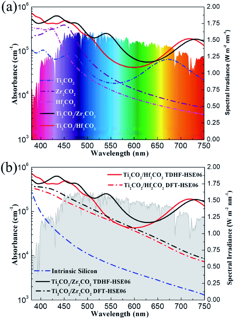
In order to utilize the solar energy efficiently, a wide adsorption range especially in the visible-light region of solar radiation is another critical factor that a high-quality solar cell should fulfill. In order to include the excitonic effect, the optical absorption properties of the Ti2CO2/Zr2CO2 and Ti2CO2/Hf2CO2 vdW heterostructures and the isolated monolayers calculated by the TDHF-HSE06 method are plotted in Fig. 6a. As is seen, the Ti2CO2/Zr2CO2 and Ti2CO2/Hf2CO2 vdW heterostructures exhibit broad optical absorptions, where the absorption coefficients can reach 6 × 105 cm−1 and 7 × 105 cm−1, respectively. In addition, the optical adsorptions of vdW heterostructures are more noticeable than those of the corresponding isolated monolayers. This is due to the expanded overlap between the absorption edge and the solar spectrum caused by the reduced band gaps of the vdW heterostructures, which can also be observed in many other 2D heterostructures.54–56 Moreover, the absorption intensity in hybrid systems can also be enhanced by the increased optical transitions induced by the interaction between the two heterostructures.5 We have also calculated the absorption coefficients of vdW heterostructures by the DFT-HSE06 (excluding the excitonic effect) approach displayed in Fig. 6b for reference. The measured bulk silicon absorbance is plotted for comparison as well.57 As compared to the standard DFT-HSE06 result, the absorption estimated by the TDHF-HSE06 method is absolutely higher, demonstrating a large excitonic effect in all visible-light ranges, which can enhance the absorption coefficients. Unlike silicon and many other 2D materials,58 the light absorbance of which descends dramatically at visible-light wavelengths, the Ti2CO2/Zr2CO2 and Ti2CO2/Hf2CO2 vdW heterostructures show remarkable light absorption in the whole visible-light region. The outstanding optical performance implies that these two vdW heterostructures are very promising high-efficiency solar cells.
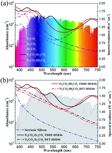 |
| | Fig. 6 Calculated TDHF-HSE06 optical absorption coefficients of Ti2CO2/Zr2CO2 and Ti2CO2/Hf2CO2 heterostructures (a) compared with those of pristine Ti2CO2, Zr2CO2, and Hf2CO2 monolayers, and (b) compared with the absorption coefficients obtained by the DFT-HSE06 method and the experimental spectrum of intrinsic silicon. The colorful and gray background indicates the reference solar spectral irradiance.53 | |
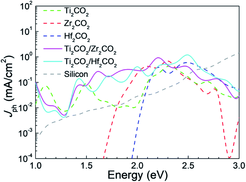
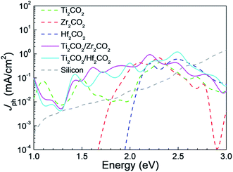
Furthermore, we have explored the photocurrents of the vdW heterostructures and corresponding isolated monolayers in device form in Fig. 7, where the photocurrents of silicon solar cell devices59 are shown for comparison as well. It is seen that the photocurrents generated in the vdW heterostructures are stronger than those of the MXene monolayers. There are two photocurrent peaks at about 1.6 eV and 2.2 eV for the Ti2CO2/Zr2CO2 vdW heterostructure device, while four peaks at about 1.5 eV, 1.7 eV, 2 eV, and 2.5 eV for the Ti2CO2/Hf2CO2 vdW heterostructure device. Additionally, the photocurrents of both the vdW heterostructure devices exceed that of the thin-film silicon device59 below 2.6 eV. The local density of states along the transport direction of solar cell devices used in our calculations is illustrated in Fig. S11,† which indicates that the device size applied in our calculations is long enough.
 |
| | Fig. 7 The calculated photocurrents of Ti2CO2/Zr2CO2 and Ti2CO2/Hf2CO2 and isolated monolayer devices, and the photocurrents of silicon solar cell devices are shown for comparison as well. | |
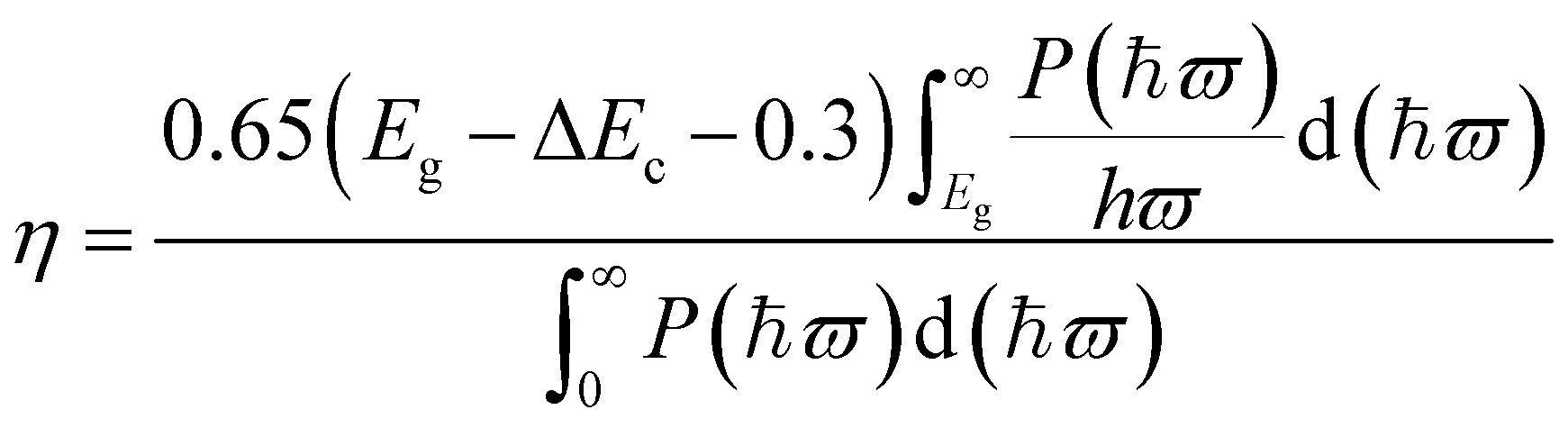
From above, the Ti2CO2/Zr2CO2 and Ti2CO2/Hf2CO2 vdW heterostructures are seen to be very promising photovoltaic solar cells with suitable band gaps and high separation efficiencies of phonon-induced carriers. Herein, to evaluate the quality of these two vdW heterostructures, we estimated the power conversion efficiency (PCE) η by an approach proposed by Scharber et al.2,63 The maximum PCE for such devices can be defined as the following equation:
| |  | (2) |
where 0.65 is the band-fill factor,
P(
ħϖ) is the AM1.5 solar energy flux at the value of
ħϖ for photon energy, and
Eg is the band gap of the donor. The integral of the numerator and denominator represents the short circuit current assuming an external quantum efficiency (EQE) of 100% and the incident solar radiation, respectively. Δ
Ec is the conduction band offset between the donor and acceptor, and the (
Eg − Δ
Ec − 0.3) term is an estimation of the maximum open circuit voltage.
Fig. 8a and b illustrate the band edge data of independent monolayers fixed in the Ti
2CO
2/Zr
2CO
2 and Ti
2CO
2/Hf
2CO
2 vdW heterostructures, respectively. Remarkably, the maximum PCEs of the Ti
2CO
2/Zr
2CO
2 and Ti
2CO
2/Hf
2CO
2 vdW heterostructures are calculated to be as high as 22.74% and 19.56%, respectively, which are highlighted as black stars in
Fig. 8c. This can be explained by the combined effects of the matched donor–acceptor band alignments and moderate band gaps of vdW heterostructures. For a more intuitive comparison, the PCEs of the vdW heterostructures and other recently 2D heterostructure solar cells are listed in
Table 2. It is concluded that the PCEs of the Ti
2CO
2/Zr
2CO
2 and Ti
2CO
2/Hf
2CO
2 vdW heterostructures will be advantageous. We have drawn the heterostructure solar cell with fluoride-doped tin oxide (FTO) transparent conductive glass electrodes in
Fig. 8d. Photon absorptions in a type-II heterostructure generate excited free carriers. Free carriers separate into electrons and holes at the donor and acceptor at an ultrafast time scale. Thus, photocurrent will be produced from electrodes during the free carrier dissociation process.
 |
| | Fig. 8 The HSE06 band structures of mutually independent monolayers fixed in the (a) Ti2CO2/Zr2CO2 and (b) Ti2CO2/Hf2CO2 heterostructure lattices. (c) Simulated solar cell power conversion efficiency contour as a function of the donor band gap and conduction band offset. (d) Schematic illustration of the Ti2CO2/Zr2CO2 heterostructure solar cell and the internal free charge carrier transfer route. | |
Table 2 Calculated maximum power conversion efficiency PCE (%) of recently designed 2D heterostructure solar cells
| System |
PCE |
References |
| Ti2CO2/Zr2CO2 |
22.74 |
This work |
| Ti2CO2/Hf2CO2 |
19.56 |
This work |
| HfTeSe4/Bi2WO6 |
20.8 |
60
|
| Te/WTe2, Te/MoTe2 |
22.5, 20.1 |
5
|
| GaTe/InS, GaTe/GaSe |
11.52, 18.39 |
50
|
| TiNF/TiNCl, TiNCl/TiNBr |
22, 19 |
22
|
| ZrS3/HfS3 |
16–18 |
61
|
| MoSe2/ψ-phosphorene |
20.26 |
62
|
| α-AsP/GaN |
22.1 |
51
|
| Edge-modified phosphorene nanoflakes |
20 |
3
|
| MoS2/bilayer phosphorene |
16–18 |
63
|
| Phosphorene/MoS2 heterobilayer |
17.5 |
64
|
4. Conclusions
In summary, by first-principles hybrid functional calculations, we have comprehensively screened the electronic structures of 2D MXenes for application as solar cell donor and acceptor materials, among which the band gaps of Ti2CO2, Zr2CO2, and Hf2CO2 meet the requirement for combining thin film solar cells. Taking the band edge positions into account, the Ti2CO2/Zr2CO2 and Ti2CO2/Hf2CO2 vdW heterostructures were proposed to study their optoelectronic characteristics. Firstly, the dynamic and thermal stabilities of these two vdW heterostructures have been confirmed by phonon dispersion and AIMD simulations, respectively. The type-II donor–acceptor interface band alignment dissociates electron–hole pairs into free charge carriers in different layers, while the high and directionally anisotropic carrier mobility further reduces carrier recombination rates. The combined systems exhibit very good optical absorptions at visible-light wavelengths due to the moderate band gaps. Moreover, the designed Ti2CO2/Zr2CO2 and Ti2CO2/Hf2CO2 vdW heterostructures can achieve very high superior PCEs of up to 22.74% and 19.56%, respectively, the photocurrents of which are competitive with those of silicon solar cell devices. Our present study highlights MXenes for application as both a donor and acceptor for thin film solar cells and further guides the design of more 2D semiconductors for photovoltaic materials.
Conflicts of interest
The authors declare no competing financial interest.
Acknowledgements
This work was supported by the National Key Research and Development Program of China (No. 2017YFB0701701), the National Natural Science Foundation of China (No. 21973012, 51872017 and 51871009), the Natural Science Foundation of Fujian Province (No. 2020J01351) and the ‘‘Qishan Scholar’’ Scientific Research Project of Fuzhou University.
References
- W. Shockley and H. J. Queisser, J. Appl. Phys., 1961, 32, 510–519 CrossRef CAS.
- M. C. Scharber, D. Mühlbacher, M. Koppe, P. Denk, C. Waldauf, A. J. Heeger and C. J. Brabec, Adv. Mater., 2006, 18, 789–794 CrossRef CAS.
- W. Hu, L. Lin, C. Yang, J. Dai and J. Yang, Nano Lett., 2016, 16, 1675–1682 CrossRef CAS.
- K. Cheng, Y. Guo, N. Han, Y. Su, J. Zhang and J. Zhao, J. Mater. Chem. C, 2017, 5, 3788–3795 RSC.
- K. Wu, H. Ma, Y. Gao, W. Hu and J. Yang, J. Mater. Chem. A, 2019, 7, 7430–7436 RSC.
- H. Y. Wu, K. Yang, Y. Si, W. Q. Huang, W. Y. Hu and G. F. Huang, Phys. Status Solidi RRL, 2019, 13, 8 Search PubMed.
- Z. Guo, N. Miao, J. Zhou, B. Sa and Z. Sun, J. Mater. Chem. C, 2017, 5, 978–984 RSC.
- H. Wang, R. Peng, Z. D. Hood, M. Naguib, S. P. Adhikari and Z. Wu, ChemSusChem, 2016, 9, 1490–1497 CrossRef CAS.
- J.-C. Lei, X. Zhang and Z. Zhou, Front. Phys., 2015, 10, 276–286 CrossRef.
- X. Zhan, C. Si, J. Zhou and Z. Sun, Nanoscale Horiz., 2020, 5, 235–258 RSC.
- B. Anasori, M. R. Lukatskaya and Y. Gogotsi, Nat. Rev. Mater., 2017, 2, 1–17 RSC.
- P. Xiong, B. Sun, N. Sakai, R. Ma, T. Sasaki, S. Wang, J. Zhang and G. Wang, Adv. Mater., 2019, 32, 1902654 CrossRef.
- M. Naguib, V. N. Mochalin, M. W. Barsoum and Y. Gogotsi, Adv. Mater., 2014, 26, 992–1005 CrossRef CAS.
- A. D. Handoko, S. N. Steinmann and Z. W. Seh, Nanoscale Horiz., 2019, 4, 809–827 RSC.
- Z. Guo, J. Zhou, L. Zhu and Z. Sun, J. Mater. Chem. A, 2016, 4, 11446–11452 RSC.
- C.-F. Fu, X. Li, Q. Luo and J. Yang, J. Mater. Chem. A, 2017, 5, 24972–24980 RSC.
- H. Zhang, G. Yang, X. Zuo, H. Tang, Q. Yang and G. Li, J. Mater. Chem. A, 2016, 4, 12913–12920 RSC.
- M. R. Lukatskaya, O. Mashtalir, C. E. Ren, Y. Dall'Agnese, P. Rozier, P. L. Taberna, M. Naguib, P. Simon, M. W. Barsoum and Y. Gogotsi, Science, 2013, 341, 1502–1505 CrossRef CAS.
- Y. Wang, X. Yu, S. Xu, J. Bai, R. Xiao, Y.-S. Hu, H. Li, X.-Q. Yang, L. Chen and X. Huang, Nat. Commun., 2013, 4, 2365 CrossRef.
- M. Ghidiu, M. R. Lukatskaya, M.-Q. Zhao, Y. Gogotsi and M. W. Barsoum, Nature, 2014, 516, 78–81 CrossRef CAS.
- Q. Peng, J. Guo, Q. Zhang, J. Xiang, B. Liu, A. Zhou, R. Liu and Y. Tian, J. Am. Chem. Soc., 2014, 136, 4113–4116 CrossRef CAS.
- Y. Liang, Y. Dai, Y. Ma, L. Ju, W. Wei and B. Huang, J. Mater. Chem. A, 2018, 6, 2073–2080 RSC.
- M. Khazaei, M. Arai, T. Sasaki, C. Y. Chung, N. S. Venkataramanan, M. Estili, Y. Sakka and Y. Kawazoe, Adv. Funct. Mater., 2013, 23, 2185–2192 CrossRef CAS.
- M. Khazaei, A. Ranjbar, M. Arai, T. Sasaki and S. Yunoki, J. Mater. Chem. C, 2017, 5, 2488–2503 RSC.
- G. Kresse and J. Furthmüller, Phys. Rev. B, 1996, 54, 11169 CrossRef CAS.
- G. Kresse and D. Joubert, Phys. Rev. B, 1999, 59, 1758 CrossRef CAS.
- P. E. Blöchl, Phys. Rev. B, 1994, 50, 17953 CrossRef.
- J. P. Perdew, K. Burke and M. Ernzerhof, Phys. Rev. Lett., 1996, 77, 3865 CrossRef CAS.
- S. Grimme, J. Antony, S. Ehrlich and H. Krieg, J. Chem. Phys., 2010, 132, 154104 CrossRef.
- V. I. Anisimov, F. Aryasetiawan and A. Lichtenstein, J. Phys.: Condens. Matter, 1997, 9, 767 CrossRef CAS.
- S. Dudarev, G. Botton, S. Savrasov, C. Humphreys and A. Sutton, Phys. Rev. B, 1998, 57, 1505 CrossRef CAS.
- Z. Hu and H. Metiu, J. Phys. Chem. C, 2011, 115, 5841–5845 CrossRef CAS.
- Y. Zhang, X.-H. Zha, K. Luo, N. Qiu, Y. Zhou, J. He, Z. Chai, Z. Huang, Q. Huang and Y. Liang, J. Phys. Chem. C, 2019, 123, 6802–6811 CrossRef CAS.
- Q. Peng, J. Zhou, J. Chen, T. Zhang and Z. Sun, J. Mater. Chem. A, 2019, 7, 26062–26070 RSC.
- M. Marsman, J. Paier, A. Stroppa and G. Kresse, J. Phys.: Condens. Matter, 2008, 20, 064201 CrossRef CAS.
- F. Furche and R. Ahlrichs, J. Chem. Phys., 2002, 117, 7433–7447 CrossRef CAS.
- A. Togo, F. Oba and I. Tanaka, Phys. Rev. B, 2008, 78, 134106 CrossRef.
- X. Gonze and C. Lee, Phys. Rev. B, 1997, 55, 10355 CrossRef CAS.
- S. Smidstrup, T. Markussen, P. Vancraeyveld, J. Wellendorff, J. Schneider, T. Gunst, B. Verstichel, D. Stradi, P. A. Khomyakov, U. G. Vej-Hansen, M.-E. Lee, S. T. Chill, F. Rasmussen, G. Penazzi, F. Corsetti, A. Ojanperä, K. Jensen, M. L. N. Palsgaard, U. Martinez, A. Blom, M. Brandbyge and K. Stokbro, J. Phys.: Condens. Matter, 2019, 32, 015901 CrossRef.
- R. Marschall, Adv. Funct. Mater., 2014, 24, 2421–2440 CrossRef CAS.
- X. Zhang, X. Zhao, D. Wu, Y. Jing and Z. Zhou, Nanoscale, 2015, 7, 16020–16025 RSC.
- G. Rehman, S. Khan, B. Amin, I. Ahmad, L.-Y. Gan and M. Maqbool, J. Mater. Chem. C, 2018, 6, 2830–2839 RSC.
- X. Li, Y. Dai, Y. Ma, Q. Liu and B. Huang, Nanotechnology, 2015, 26, 135703 CrossRef.
- Z. Guo, J. Zhou, C. Si and Z. Sun, Phys. Chem. Chem. Phys., 2015, 17, 15348–15354 RSC.
- J. Liao, B. Sa, J. Zhou, R. Ahuja and Z. Sun, J. Phys. Chem. C, 2014, 118, 17594–17599 CrossRef CAS.
- T. Björkman, A. Gulans, A. V. Krasheninnikov and R. M. Nieminen, Phys. Rev. Lett., 2012, 108, 235502 CrossRef.
- F. Zheng, L. Z. Tan, S. Liu and A. M. Rappe, Nano Lett., 2015, 15, 7794–7800 CrossRef CAS.
- N. Miao, B. Xu, N. C. Bristowe, J. Zhou and Z. Sun, J. Am. Chem. Soc., 2017, 139, 11125–11131 CrossRef CAS.
- J. Wang, H. Chen, S. H. Wei and W. J. Yin, Adv. Mater., 2019, 31, 1806593 CrossRef.
- J. Chen, X. He, B. Sa, J. Zhou, C. Xu, C. Wen and Z. Sun, Nanoscale, 2019, 11, 6431–6444 RSC.
- M. Xie, S. Zhang, B. Cai, Y. Huang, Y. Zou, B. Guo, Y. Gu and H. Zeng, Nano Energy, 2016, 28, 433–439 CrossRef CAS.
- X.-H. Zha, J. Zhou, Y. Zhou, Q. Huang, J. He, J. S. Francisco, K. Luo and S. Du, Nanoscale, 2016, 8, 6110–6117 RSC.
-
A. G173-03, ASTM International, West Conshohocken, PA, 2012, www.astm.org Search PubMed.
- Q. Peng, Z. Wang, B. Sa, B. Wu and Z. Sun, Sci. Rep., 2016, 6, 31994 CrossRef CAS.
- C. Xia, J. Du, W. Xiong, Y. Jia, Z. Wei and J. Li, J. Mater. Chem. A, 2017, 5, 13400–13410 RSC.
- H. Jin, Y. Dai, X.-C. Ma, L. Yu, W. Wei and B.-B. Huang, RSC Adv., 2015, 5, 52264–52268 RSC.
- M. A. Green and M. J. Keevers, Prog. Photovoltaics Res. Appl., 1995, 3, 189–192 CrossRef CAS.
- Q. H. Wang, K. Kalantar-Zadeh, A. Kis, J. N. Coleman and M. S. Strano, Nat. Nanotechnol., 2012, 7, 699 CrossRef CAS.
- M. Palsgaard, T. Markussen, T. Gunst, M. Brandbyge and K. Stokbro, Phys. Rev. Appl., 2018, 10, 014026 CrossRef CAS.
- H. Yang, Y. Ma, Y. Liang, B. Huang and Y. Dai, ACS Appl. Mater. Interfaces, 2019, 11, 37901–37907 CrossRef CAS.
- Q. Zhao, Y. Guo, Y. Zhou, Z. Yao, Z. Ren, J. Bai and X. Xu, Nanoscale, 2018, 10, 3547–3555 RSC.
- H. Wang, X. Li, Z. Liu and J. Yang, Phys. Chem. Chem. Phys., 2017, 19, 2402–2408 RSC.
- J. Dai and X. C. Zeng, J. Phys. Chem. Lett., 2014, 5, 1289–1293 CrossRef CAS.
- H. Guo, N. Lu, J. Dai, X. Wu and X. C. Zeng, J. Phys. Chem. C, 2014, 118, 14051–14059 CrossRef CAS.
Footnote |
| † Electronic supplementary information (ESI) available. See DOI: 10.1039/d0se01443e |
|
| This journal is © The Royal Society of Chemistry 2021 |
Click here to see how this site uses Cookies. View our privacy policy here. 
 *b,
Jian
Zhou
*b,
Jian
Zhou