
 Open Access Article
 This Open Access Article is licensed under a Creative Commons Attribution-Non Commercial 3.0 Unported Licence
Perovskite indoor photovoltaics: opportunity and challenges
Kai-Li
Wang
a,
Yu-Hang
Zhou
a,
Yan-Hui
Lou
b and
Zhao-Kui
Wang
 *a
*a
aInstitute of Functional Nano & Soft Materials (FUNSOM), Jiangsu Key Laboratory for Carbon-Based Functional Materials & Devices, Soochow University, Suzhou, Jiangsu 215123, China. E-mail: zkwang@suda.edu.cn
bCollege of Energy, Soochow Institute for Energy and Materials Innovations, Soochow University, Suzhou 215006, China
First published on 2nd September 2021
Abstract
With the rapid development of the Internet of Things (IoTs), photovoltaics (PVs) has a vast market supply gap of billion dollars. Moreover, it also puts forward new requirements for the development of indoor photovoltaic devices (IPVs). In recent years, PVs represented by organic photovoltaic cells (OPVs), silicon solar cells, dye-sensitized solar cells (DSSCs), etc. considered for use in IoTs mechanisms have also been extensively investigated. However, there are few reports on the indoor applications of perovskite devices, even though it has the advantages of better performance. In fact, perovskite has the advantages of better bandgap adjustability, lower cost, and easier preparation of large-area on flexible substrates, compared with other types of IPVs. This review starts from the development status of IoTs and investigates the cost, technology, and future trends of IPVs. We believe that perovskite photovoltaics is more suitable for indoor applications and review some strategies for fabricating high-performance perovskite indoor photovoltaic devices (IPVs). Finally, we also put forward a perspective for the long-term development of perovskite IPVs.
1. Introduction
In high speed under the background of modernization, indoor photovoltaics (IPVs) has attracted much attention with the emergence of Big Data and the Internet of Things (IoTs), owing to the billions of product demand gap for the self-powered devices.1 The IoTs refer to things that automatically communicate wirelessly between various electronic devices through the Internet. The digital information and real-time data can be collected or exchanged by sensors, terminal devices, health monitoring, etc., which are widely used in intelligent buildings, radio-frequency identification (RFID) sensors, retail industries, and wearable devices.2–4 In the new era of IoTs, radio has raised new requirements regarding size, weight, energy consumption, and cost reduction.5 These applications are independent and off-the-grid, and it is wise and necessary to replace non-self-rechargeable batteries through power supplement via indoor photovoltaics.6 In recent years, IPV as a device to convert indoor light to electric energy has been a powerful technology in the IoTs system.7–9 For example, chalcogenide (i.e., GaSe2 and CuInGaSe2) solar cells,10,11 dye-sensitized (DSSCs),12–14 organic photovoltaic (OPVs),15,16 and perovskite solar cells (PSCs)17,18 have received significant attention in the IPVs field, owing to their advantages of simple fabrication technology, adjustable bandgap, and high performance. For optimizing IPVs, the suitable absorption spectra, large open-circuit with low energy loss, minimized trap-mediated charge recombination and leakage currents, and excellent stability of indoor photovoltaic materials and devices are the key issues.19 Furthermore, there always have been contradictions between the heavy, complex, and unsustainable portable power source and the portability of the IoTs system. The cumbersome power source becomes a burden for daily use and shortens the lifetime of mobile devices.20,21 Hence, the development of simple, lightweight, low-cost, and self-powered devices is urgent for the IoTs system.Notably, the PVs that are used to convert sunlight are not necessarily suitable for indoor applications due to the Sun's emission spectra and indoor light source. The emission spectra of indoor light sources (fluorescent lamps (FL) and light-emitting diodes (LED)) are located in the range of 200–700 nm and for solar AM1.5 spectrum is about 300–1100 nm. Meanwhile, the intensity of FL and LED are also three orders of magnitude lower than AM1.5.22,23 Therefore, choosing a light-absorbing material with a suitable bandgap to absorb the indoor light source effectively is necessary. According to the theoretical simulations, the absorber materials with a 1.8–1.95 eV bandgap are ideal for high-performance IPVs.24–26 This is the main reason that the high-performance solar cells with a bandgap from 1.1 to 1.6 eV (e.g., crystalline silicon solar cells) designed for the one solar illumination intensity are unsuitable for indoor applications.27,28 In addition, IPVs have higher requirements for defects and interface contact due to the too low indoor light source intensity that can only generate very few carriers. Park et al. demonstrated that doping chlorine into perovskite decreased the bulk defects of perovskite, which can suppress the ion migration and non-radiative recombination and improve the power density to 3.525 (231.78) μW cm−2 under 400 lux.29 Brown et al. also reported the role of interface defects on indoor flexible PSCs based on the TiO2 compact layer and the mesoporous layer, evidencing that the interface defects are crucial for the indoor performance of devices.30
In recent years, researchers have also tried to use various PV materials to absorb indoor light sources for fabricating IPVs. For example, DSSCs have been reported to perform well in indoor low-light sources. However, the high cost of this type of device limits the further development of its commercialization.31 In contrast, PSCs have the advantages of efficient processing, lightweight, and low cost, making them have great potential in the IPVs field. Considering the different emission spectra of the light source, the absorber layer material of IPVs should have a medium bandgap and a narrow absorption spectrum in the visible light range to obtain good spectral matching.32,33 Perovskite can freely adjust the bandgap without complicated synthetic routes and expensive preparation costs.34,35 Furthermore, the bandgap of perovskite materials can freely change from 1.18 to 2.6 eV by a simple solution-processed component engineering, and its excellent light absorption ability and long carrier diffusion distance are also more suitable for low light conditions.36–38
This review summarizes the market demand, cost, application field, and market trend of IPVs. We also discuss the existing issues and predict the research direction of IPVs. The device performance of various types of IPVs will be compared. We believe that perovskite indoor photovoltaics (PIPVs) have the potential to lead the IPVs industry after solving the critical issues of stability and toxicity. Finally, we will be introducing the strategies for fabricating high-performance PIPVs.
2. Perspective of indoor photovoltaics
2.1 Application potential of IPVs
The IoTs system is referred to the automatic wireless communication between various electronic devices via the Internet, i.e., real-time data collection and exchange of digital information by the electronic devices, and applied to smart home, aerospace, alarm systems, and indoor wearable technology. IPV as a mobile self-power device required in the IoTs system has diversification on the specifications, power, morphology, cost, and lighting environment to adapt to the different working environments. Therefore, IPVs have enormous potential to be used on various miniature mobile platforms, such as wearable electronic devices, wireless antennas, sensors, and biomedical treatments, as exhibited in Fig. 1a.39–41 In addition, the influence of indoor light sources must also be considered. Normally, a simulated solar source AM1.5 (100 mW cm−2) is commonly used to evaluate the performance of PVs in the laboratory.42,43 However, adequate sunlight may not always be met due to the reference of weather, environment, time, etc. Thus, the performance of PVs under artificial indoor lighting sources, such as LED, CFL, halogen lamps, and incandescent bulbs with special color appearance and different intensities (Fig. 1b) also needs to be considered.44 In the near future, light energy from the environment through IPVs for continuous power supply is necessary.45,46Fig. 1c shows an example of indoor wireless interconnection equipment with the power provided by IPVs (1 cm2). For example, organic based IPVs can achieve a good PCE of about 30% (corresponding input power of 0.521 mW cm−2 and output power of 15 μW), which is enough to drive many electronic applications (RTID tags, wristwatches, calculators and standby devices).39,47 It is worth noting that the PCE of PSCs under indoor conditions is mostly above 35%.48–50 That means the same area of PIPVs can drive more electronic devices, and it will also become an excellent candidate in the IPV field.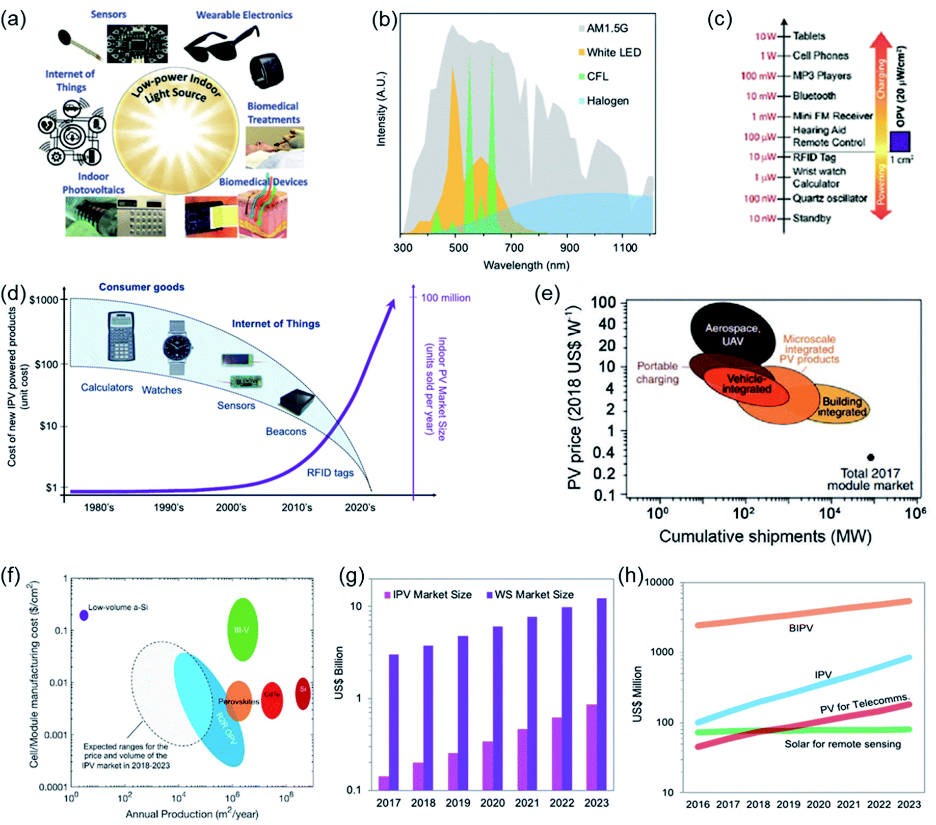 | ||
| Fig. 1 (a) The equipment obtains energy through IPVs power generation under indoor lighting conditions. Reproduced from ref. 39 with permission from the [Wiley-VCH], copyright [2018]. (b) Emission spectra of different light sources. Reproduced from ref. 45 with permission from the [Elsevier], copyright [2019]. (c) Powered by IPVs of 1 square centimeter under indoor lighting and the corresponding drivable electronic equipment. Reproduced from ref. 39 with permission from the [Wiley-VCH], copyright [2018]. (d) The cost and market size of IPVs as a function of time (years). (e) Expected market size of different photovoltaic applications (2018–2027). (f) Manufacturing cost and annual production scale and indoor usage of different types of IPVs, (g) forecast of IPVs and WS market size, and (h) market demand for photovoltaic cells/modules in different energy demand fields (2016–2023). Reproduced from ref. 45 with permission from the [Elsevier], copyright [2019]. | ||
PVs have been combined with watches, calculators, and sensors for many years (Fig. 1d), owing to the stable power output and the excellent performance under low-light sources.45,51 In addition, IPVs show great potential to create a huge market for indoor renewable energy. For example, some companies such as WSL Solar,52 Powerfilm,53 and Soelms54 are commercializing amorphous Si modules as IPVs. GCel55 and Ricoh56 are also using DSSCs as IPVs for commercialization. Particularly, amorphous Si and dye-based PVs can even drive simple devices, such as watches, calculators, and sensors at a light intensity of 20 lux.54 According to forecasts, hundreds of millions of wireless sensors will be installed indoors in the next ten years.55 It can be said that IPVs have a good development prospect even if there are still many difficulties. Among them, the greatest difficulty is the long-term stability of devices and the toxicity of materials (such as cadmium (Cd), lead (Pb), and arsenide (As)). Over the years, the manufacture of photovoltaic devices in the research and manufacturing sector has received great attention, although it has been banned in some areas because of its toxicity.57–60 In fact, Alta company recently closed its IPVs production due to the lack of suitable investors.61 This suggests that IPVs manufacturing technology must be developed rapidly in order to meet the requirements of long-term human development. In addition, it is also crucial that the IPVs can be fabricated on a flexible and large-area substrate to meet the different market needs. Photovoltaic panels can be installed directly into these types of equipment or simply installed on panels on walls, floors, or other surfaces, to nearby power equipment or return power to the building's power supply system.
In today's fast modernization, IPVs have also been rapidly developed. However, the commercialization of IPVs is still laggard compared with the development of solar modules. For example, reports show that the global market value of IPVs is only $140 million,45 which is far below the $100 billion of solar energy modules.62 We all know that in order for something new to replace something that already exists, it must have advantages that the body (human) cannot refuse, such as cost and performance. Typically, the cost of the production model is dependent on the production scale of the PV system.46,63 However, in order to fabricate low-cost IPVs, using inexpensive materials and an excellent technique process is far-sighted. This strategy is beneficial to the growth of the expected market size of different types of IPVs, which is the function of the price per watt of different equipment, as shown in Fig. 1e.45,64 Each sphere shows the forecast of the market size (horizontal span) and price per watt (vertical span) from 2018 to 2027. In the next ten years (2018–2027), PVs will be mainly used in integrated buildings (approximately two orders of magnitude increase), and its price per watt will also have a great price advantage in the possible equipment. To realize the vision of the IoTs ecosystem, i.e. billions of sensor nodes and wireless antenna connected to the network, relying on a single node to reduce power usage is the most effective method. In recent years, the research trend of energy efficiency and low power hardware protocols is to solve this problem, improve energy efficiency to reduce latency, and improve data reliability.65,66Fig. 1f shows the comparison of the production of system units based on low-volume amorphous Si, III–V, PSCs, CdTe, and Si compounds with the annual production volume. Among them, OPV, PSCs, and CdTe based cells have lower cost.45,66 In addition, within the range of 5 years, the OPV devices show lower costs if using the R2R method.
PV cells used as indoor wireless node power supply systems can promote the growth of the IPV market. The current global market for IPV cells is $140 million.45,67 The estimated size of the wireless sensor (WS) and IPVs market in the next ten years (2017–2023) is billions of dollars (Fig. 1g).45 The IPV market will experience a spurt of development in the next ten years, reaching $850 million in 2023 and hopefully exceed a billion dollars in the following years. By 2023, the market demand for photovoltaic energy is expected to reach 60 million units per year.67 In addition, Fig. 1h shows the forecast for the next 8 years (2018–2023). IPVs not only form a part of the building integration PVs (BIPV) to obtain a higher market value ratio, but also continue to exhibit a higher market ratio relative to PVs used for remote sensing and telecommunications.45 This means that IPVS will become an integral part of the power ecosystem for the Internet of Things. In addition, the global IPV market is expected to grow to $5.1 billion in 2023, representing an annual growth rate of 33.6 percent.68
2.2 Research progress of IPVs
When there is no solar radiation, IPVs mainly collect the energy emitted by the artificial light source (CFL, LED, incandescent, halogen). The illumination intensity is usually three orders of magnitude lower than the sunlight. The difference in the light source directly leads to the difference in the spectral range and the bandgap of the matching absorber. Fig. 2a shows the maximum limit PCEs of PVs under different indoor light sources, according to the detailed equilibrium limit theory and Shockley and Queisser.24,69 This calculation is performed based on the assumption that the above bandgap energy of all absorbed under different lighting conditions, and the carrier was completely extracted. We can find that the optimal bandgap for AM1.5 is ca. 1.34 eV, and for the indoor light source (LED and CFL) is ca. 1.9 eV. Surprisingly, the maximum theoretical efficiency of 1.9 eV bandgap material can be close to 60% when IPVs are under the 3-color LED condition. However, under the condition of AM1.5, the calculated efficiency limit of PVs with a bandgap of 1.1 eV does not exceed 40%. This is due to the light absorption range of the absorber with a bandgap of 1.9 eV almost perfectly covering the indoor light source spectrum (200–700 nm), making the photons be fully utilized by active materials under indoor light sources with a narrow spectrum. Meanwhile, compared with sunlight, indoor light sources can achieve higher efficiency due to the narrower spectral band reducing the transparency loss and thermal loss associated with the broadband solar spectrum.70 This is the reason for silicon-based solar cells having lower PCE under the indoor lighting conditions compared with OPVs or PSCs.71–74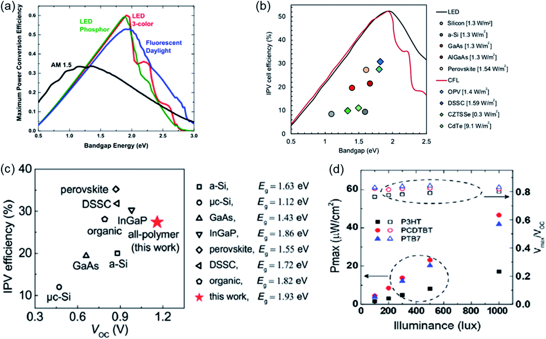 | ||
| Fig. 2 (a) The bandgap of the light-absorbing layer material under different light sources and the maximum photoelectric conversion efficiency of the corresponding IPV. Reproduced from ref. 24 with permission from the [Institute of Electrical and Electronics Engineers Inc], copyright [2015]. (b) The statistics of maximum efficiency (under CFL and LED illumination) and bandgap for IPVs, so far. Reproduced from ref. 45 with permission from the [Elsevier], copyright [2018]. (c) The PCE and Voc distribution of various types IPVs under the indoor light source. Reproduced from ref. 96 with permission from the [Royal Society of Chemistry], copyright [2019]. (d) OPVs maximum power output density and Vmax/Voc ratio under indoor light source. Reproduced from ref. 77 with permission from the [American Institute of Physics], copyright [2016]. | ||
In addition, it is challenging to accurately estimate indoor performance since there is no recognized standard for indoor spectral quality and irradiance (e.g., AM1.5 for the outdoor standard). Lin et al. summarized the existing indoor light intensity measurement defects by lux meter, which essentially explained the irregularity of the existing test standards.75 Thus, a universal, standard, and accurate indoor spectroscopy method and equipment are necessary. In recent years, OPVs, DSSCs, and GaAs based IPVs have been developed rapidly. CFL and LED are commonly used as indoor light sources to evaluate the performance of IPVs. As shown in Fig. 2b, Peters et al. used a detailed efficiency balance limit method to calculate the theoretical maximum efficiency of IPVs (i.e., Si, GaAs, OPV, and perovskite based IPV) under 1 W m−2 of CFL and LED lighting.45 The PCE of perovskite-based IPVs is higher than the others. Notably, the maximum PCE values of IPVs can reach an astonishing 52% under the indoor light source of CFL and LED illuminations. Currently, the efficiency of IPVs is around 40%. Notably, it cannot obtain a higher Voc due to the mismatch of the optical bandgap (<2 eV).
Silicon, a dominant cell material, and the Si-based solar cells with record solar PCE is over 26% under AM1.5. However, this type of PVs demonstrates an incompatible PCE of 8% under the indoor light source.76–80 To overcome the limitation of the bandgap of crystalline silicon in IPVs, amorphous silicon (a-Si, the bandgap is wider, 1.6 eV) has become one of the leading technologies in indoor photovoltaics. Shieh et al. reported a p-a-SiC:H window layer that was used to enhance the efficiency of amorphous Si-based solar cells to 25.56 μW cm−2 under 500 lux.81 In addition, CdTe and CIGS are the most successful photovoltaic materials than silicon. However, CIGS has a low shunt resistance under low light conditions, resulting in a significant decrease in the efficiency of devices as the light intensity decreases.82 In contrast, CdTe (with a bandgap of 1.5 eV) based IPVs can maintain high performance under diffuse radiation and indoor light sources, which could have promoted its establishment of a strong commercial advantage in the photovoltaic market.83 However, a relatively small amount of public data indicates that CdTe-based IPVs are only 10.9% efficient under CFL lighting conditions, which is not enough to advance the CdTe-based IPVs.84 Analogously, Cu2ZnSn(S,Se)4 (CZTSSe) thin film cells also have efficiencies approaching 10% under CFL and AM1.5G spectra.85 Among the existing IPVs, GaAs based solar cells are extremely competitive, and their efficiency exceeds 20% on the flexible substrates under low light indoor sources.86,87 Initially, some materials were used to optimize the bandgap close to 2 eV, such as GaxIn1−xP and AlxGaAs (1.8–1.9 eV) to obtain a higher efficiency under LF or LDE. However, the experimental results showed similar efficiency as GaAs, GaInP, and AlGaAs-based IPVs under an indoor light source.86,88,89 OPVs, a high-performance PV with adjustable bandgap and high absorption for visible light region spectrum, has been developed rapidly in recent years. The best efficiency of OPVs has reached 17.8% with AM1.5 illimitations,90 and more than 28% efficiency was obtained under an indoor light source (1000 lux) using materials with a bandgap of 1.8 eV.91 Furthermore, dye-sensitized IPVs also shows excellent performance under low light conditions, and optimal efficiency of 31.8% was demonstrated under CFL illuminance (1000 lux).92,93 Recently, Freitag et al. reported more than 34% efficiency under 1000 lux for DSSCs based on a copper(II/I) electrolyte, and the large-area (16 cm2) devices were used to power machine learning on wireless nodes.94 Very recently, Grätzel et al. reported the highest efficiency of 34.5% under 1000 lux for DSSCs with copper(II/I)-based electrolyte, indicating that this type of photovoltaics still occupies a leading position in the field of IPVs.95
In 2019, Liu et al. summarized the PCE, Voc, and bandgap of various types of IPVs, such as Si thin-film, perovskite, GaAs, InGaP, DSSCs, and OPVs based IPVs (Fig. 2c).96–102 As the optical bandgap increases (1.15–2 eV), corresponding IPVs often show higher Voc and PCE under indoor light source illumination. It is worth mentioning that PSCs have an indoor PCE of close to 40% (corresponding to an optical bandgap of only 1.55 eV) due to their excellent light absorption and defect tolerance. Regarding the performance of IPVs under different indoor light sources, it is necessary to consider the effects of different materials on Jsc, Voc, and FF (Fig. 2d).77,96 Taking OPVs as an example, Jsc can be related to the absorption of the donor material, which depends on the energy gap. Normally, in most PVs, Jsc is approximately linearly proportional to the intensity of the incident light.103–105 The Voc is a parameter related to light intensity 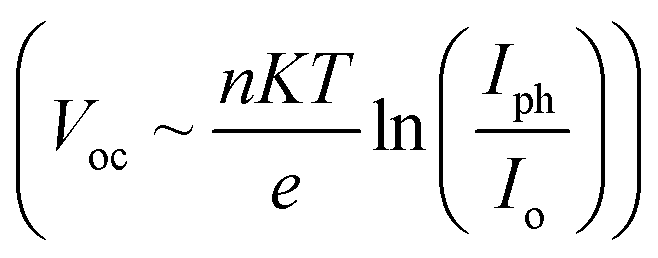 .106–108 Then, the ΔV between indoor and outdoor illumination can be estimated as
 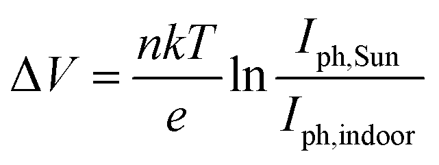 . Thus, Voc will increase with the increasing light intensity, which explains the additional loss (∼0.2 eV) of PVs under indoor light conditions.109,110 In addition, for all systems, FF increases as the light intensity decreases. Under indoor lighting conditions, the FF of each system will be significantly higher than that under the AM1.5 condition.111,112
2.3 The accurate measurement of indoor photovoltaic
There is a clear difference between the indoor and outdoor photovoltaic performance of PVs. It is essential to evaluate the photovoltaic performance of IPVs accurately. Various indoor light sources are used in daily life, including indirect sunlight, fluorescent lamp, incandescent lamp, halogen lamp, LED bulbs, and other light sources with low light intensity (200–1000 lux). Normally, the indoor light intensity is described as illumination (lux) because the human eye is sensitive to the light spectrum. So, the illumination of the indoor light source can be converted using the corresponding incident power as equation:113where the V(λ) is CIE spectral luminosity factor for human photopic vision and Km is equal to 683 lm W−1.
In addition, accurate light source calibration and test conditions are the keys to measure the performance of IPVs accurately. Wong et al. proposed calibrating indoor light sources using a general LED lux meter with NIST-traceable calibration (e.g., Extech LT40 NIST) and recommended that the maximum power point Pmax and PCE values be used to measure the device performance accurately.113 Very recently, Hou et al. proposed that the accurate test of IPVs should include the following parts. (1) The time instability of the light source for indoor PV measurement should be less than 2%. PV test should be carried out in the illumination area where the spatial distribution of light intensity is less than 2%. (2) Use a mask with the same or larger size than the transparent substrate of the cells to test the photoelectric conversion efficiency. (3) The spectrometer is more suitable for indoor light source calibration than the lux meter. Meanwhile, they also suggested that the comparison difference between Jsc (EQE) and Jsc (I–V) < 5% is suitable for verifying the accuracy of the test.114 In general, in order to accurately measure the indoor photovoltaic performance, it is necessary to use a spectrometer to calibrate the light source and select the appropriate light source. Meanwhile, the light source parameters (such as light intensity, lux, etc.) and power parameters should also be included in the device performance description.
3. Research direction of IPVs
Like outdoor photovoltaics, the efficiency, life (stability), and cost of IPVs are the key to measuring the technical feasibility of the commercialization of photovoltaic devices (Fig. 3a).35,115 In addition, large-area, flexible and modular IPVs play a particularly important role in the industrialization of IPVs. This section will summarize the development direction of IPVs from these parts.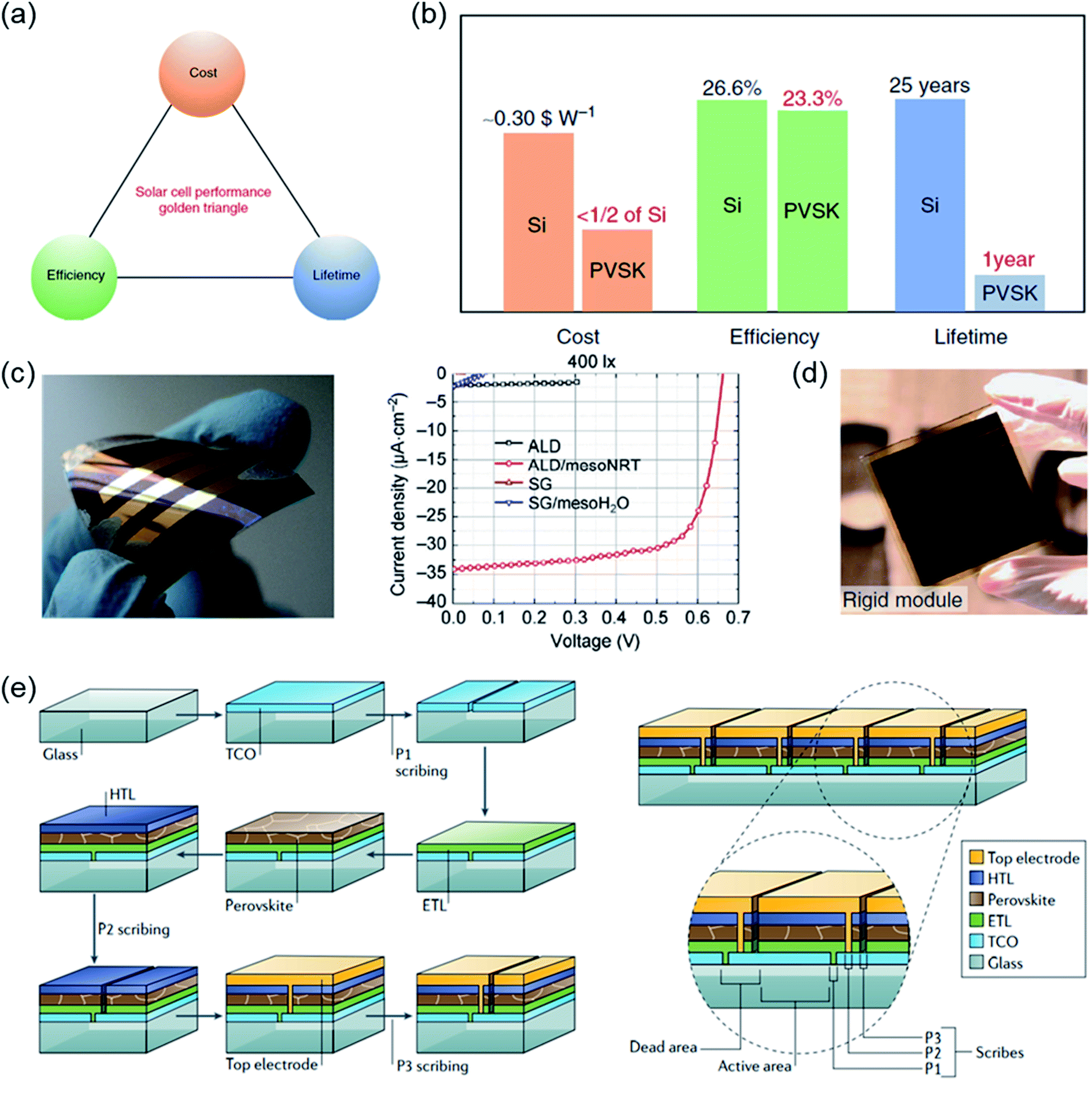 | ||
| Fig. 3 (a) The golden triangle of solar cell development and (b) comparison of perovskite solar cells and silicon solar cells. Reproduced from ref. 35 with permission from the [Nature Publishing Group], copyright [2018]. (c) The picture of a flexible solar cell and the J–V curves of the best-performing devices under 400 lux under the LED light. Reproduced from ref. 30 with permission from the [Tsinghua University Press], copyright [2018]. (d) Rigid PSCs module. Reproduced from ref. 76 with permission from the [Nature Publishing Group], copyright [2018]. (e) The schematic diagram of perovskite large-area modules. Reproduced from ref. 136 with permission from the [Nature Publishing Group], copyright [2018]. | ||
3.1 Low-cost and stable IPVs
The comprehensive level of IPVs, i.e., cost, efficiency, and stability, determines whether it can occupy a prominent position in today's competitive market of emerging photovoltaic technology.116 Furthermore, the overall cost of IPVs is determined by individual costs and lifetime, reducing the individual costs, enhancing the lifetime of single devices, increasing the effective output time, and reducing the maintenance costs. At present, the new generation thin film PVS represented by single perovskite cells has high PCE (more than 40% under 1000 lux) and low manufacturing cost (reach half of crystalline Si).117,118 However, the longest life (stability) of perovskite PV is estimated to be only one year (Fig. 3b).35 It is not enough to change the fact that the inherent lifetime of thin-film IPVs is much lower than silicon-based cells (∼25 years), even if considering the indoor working environment has relatively stable temperature and humidity. Further investigation reveals that most life expectancy is reported only for PV samples, and these samples do not meet the current industry standards.119 Thus, further improvement of the lifetime of thin film-based IPVs is necessary for their industrialization. Meanwhile, we also notice that the most reported lifetime-related investigation is conducted on un-encapsulated samples, which do not meet current industry standards.120–122 Furthermore, the encapsulation technique can effectively improve the lifetime while maintaining the performance of PVs. In fact, the encapsulation of PVs must be considered for real applications, even if its cost is estimated to exceed 60% of the total cost of PVs.123 Therefore, reducing the packaging cost is a necessary condition for the industrialization of IPVs, and in-depth research on cheap materials and packaging technology is of great importance. In addition, different levels of water vapor transmittance are considered, i.e., glass (zero) and flexible barriers (10−1 to 10−6 g per m2 per day), an excellent encapsulation technology, and packing materials are critical to the lifetime of IPVs.3.2 Flexible IPVs
For the IoTs system, it is better for IPVs to be flexible to match the multi-scene applications. Flexible IPVs can be combined on mobile platforms, i.e., buildings, watches, backpacks, and portable power supplies. Currently, indium tin oxide (ITO) film is widely used in the PV industry. However, the high processing temperature, brittleness, and manufacturing cost of ITO films limit their applications in wear-resistant, durable, and flexible IPVs.124 Therefore, the development of flexible substrates or electrode materials with high conductivity, high transmittance, durability, and lightness has a great effect on the IPVs industrialization. Furthermore, the mechanical flexibility of electrodes must be considered because IPVs usually have curved shapes or flexible features. Considering the lower light intensity of the indoor light source, the substrate or transparent conducting electrode (TCE) must be highly transparent and have a smooth surface, which allows the maximum number of photons to pass through and minimizes the recombination center to avoid current leakage. Currently, flexible electronics, i.e., graphene, conductive polymers, and silver nanowires, have been widely introduced into IPVs.125–127 Notably, as one of the most commonly used flexible substrate materials, PET is widely used in flexible PIPVs. Until now, the vast majority of flexible PVs are fabricated on this substrate. In 2016, Brown et al. reported that the flexible PIPVs based on CH3NH3PbI3−xClx reached 10.8% and 12.1% efficiencies under 200 lux and 400 lux lighting conditions, respectively (Fig. 3c).30 Park et al. demonstrated that butyl acetate (BA) replaces the CB-treated perovskite films during spin coating, which can improve the gradual nucleation and the growth of grains. The optimal devices exhibit a remarkable maximum power density of 0.063 mW cm−2 and efficiency of 23.33% under 400 lux.128 Brown et al. fabricated flexible perovskite modules and cells based on a combination of SnO2 and mesoporous-TiO2. The devices of a mesoporous TiO2 scaffold layer over SnO2 exhibited better indoor performance. For example, the cells have maximum power densities of 9.77 and 19.2 μW cm−2 under 200 and 400 lux illuminations, respectively.129 In 2020, Brown et al. reported flexible perovskite solar cells based on the roll-to-roll ITO-coated ultra-thin flexible glass (FG) substrates. The optimized devices based on FG incorporated a mesoporous scaffold over SnO2 compact layers and obtained a record efficiency of 20.6% (16.7 μW cm−2) and 22.6% (35.0 μW cm−2) under 200 and 400 lux LED illumination, respectively.48 It is believed that in the near future, there will be more and more researches and reports on flexible PIPVs. In addition, some reports on ITO-free flexible PVs can promote the further development of flexible PIPVs due to their good stretchability and flexibility.130–1333.3 Large-area IPVs
Since the light intensity of the indoor light source is ten times lower than AM1.5, the production of large-area IPVS can effectively meet the requirement of various power equipment by increasing the output power of a single cell. The output power of single-cell PVs depends on the device type (e.g., OPVs, DSSCs, and CuInGaAe). The output power of single-cell PVs with a small area (<1 cm2) has also been significantly improved in recent years. Meanwhile, many techniques like laser scribing and screen printing for the fabrication of the functional layer have been developed.134,135 As shown in Fig. 3d, the large-area fabrication of PV modules is inseparable from the application of these techniques.76 At the same time, in order to meet the requirements of more application platforms, it is necessary for IPVs to develop a higher output voltage or current by connecting individual cells in series with other techniques (such as laser etching). As shown in Fig. 3e, the fabrication of IPV modules requires multiple etching (at least three times), and the accuracy, width, and position of the slit will directly determine the overall output of the module.1364. Challenges and opportunities of PIPVs
4.1 Overview of PIPVs
Perovskite is a magical photovoltaic material in the photovoltaic field in recent years. PSCs have many advantages, such as low cost, efficiency, and large easy area fabrications, which are expected to become the mainstay of the photovoltaic industry in the future. The certified efficiency in the laboratory has approached 25.5% under AM1.5 radiation.137–143 Recently, these types of cells have shown high indoor PCE exceeding 35%.144–147 It is worth mentioning that perovskite benefits from its excellent properties by repeatedly exhibiting higher PCE under the same bandgap conditions. Furthermore, the advantages of the easy solution process, large area, and flexibility are very important to drive PIPVs on the road to industrialization. Meanwhile, perovskite materials (CsSnI3, MAPbI3, MAFAPbI3, CsPbI3, and CsPbBrI2, etc.) show variable bandgap (1.18–2.6 eV), enabling them to be fabricated as high-performance PIPVs for the specific indoor light source. Undeniably, there are still many difficulties on the road to the commercialization of PIPVs. Although the leakage of lead can be effectively reduced through physical encapsulating, it cannot essentially reduce the use of lead.148–150 Number of PSCs based companies have recently focused on developing related products but have still not applied these in the IoTs market. Fortunately, the recent rise of tin-based perovskite solar cells has completely replaced the use of the toxic element lead with tin.151–153 This may be the new hope for PIPV to move towards industrialization.4.2 Wide range of bandgap
Perovskite materials have a wide range of adjustable forbidden bandwidths, making them particularly attractive in multijunction tandem solar cells and IPVs. Many reviews have summarized the perovskite materials and developments of single cells and tandem PSCs.154–159 In this section, we aim to overview the adjustable bandgap of perovskite materials and their application in PIPVs. Metal halides perovskite crystal is described as an ABX3 structure, where A is a monovalent cation (MA, FA, Cs, and Rb), B is a kind of divalent metal cation (Pb, Sn, and Ge), and X is a halide anion (I, Br, and Cl).160 The application of PSCs began with methylammonium lead iodide (MAPbI3) with a bandgap of 1.55 eV,161,162 developed to replace cations and anions and expanded to other perovskite compositions.163 As shown in Fig. 4a, the bandgap of the perovskite film can be continuously adjusted from infrared (1.15 eV) to ultraviolet (up to 3 eV) by the composition engineering of mixed cations or anions.164 Perovskite material has a wide range of continuous bandgap adjustment ability, so it is an ideal candidate for IPVs, and can also be used for the preparation of PVs in special environments (e.g., microwaves and infrared).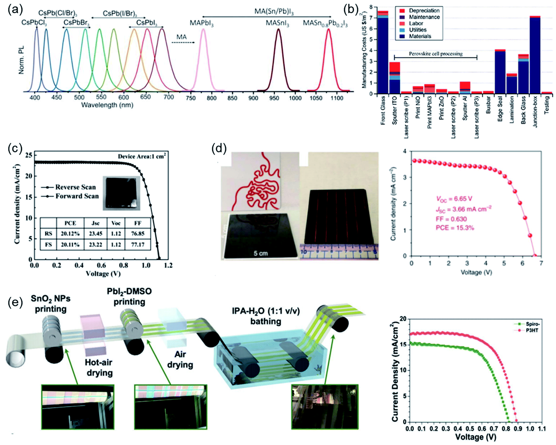 | ||
| Fig. 4 (a) Different component perovskite materials and corresponding PL peaks. Reproduced from ref. 164 with permission from the [John Wiley and Sons Ltd], copyright [2019]. (b) Statistics on the cost of perovskite photovoltaic modules. Reproduced from ref. 115 with permission from the [Royal Society of Chemistry], copyright [2017]. (c) The photo and J–V curve of PSCs (area is 1 cm2). Reproduced from ref. 177 with permission from the [Nature Publishing Group], copyright [2017].177 (d) The photograph of 5 × 5 cm MAPbI3 films and J–V curves of PSCs (active area is 12.0 cm2). Reproduced from ref. 182 with permission from the [Nature Publishing Group], copyright [2018]. (e) Schematic diagram of PSCs fabricated by the R2R process and the corresponding J–V curve. Reproduced from ref. 185 with permission from the [Wiley-VCH], copyright [2014].185 | ||
The device performance of PVs is the basis for the fabrication of high-performance PIPVs, which determines the output power of single-cell and multi-cell PIPVs. For example, the highest theoretical PCE limit of perovskite is 31%, which is far higher than the laboratory record efficiency (∼25%).165 Therefore, selecting perovskite materials with a matching bandgap from the existing mature PSCs to fabrication of PIPVs can avoid the performance degradation caused by the technology level. At present, the high-performance perovskite materials CsPbBrI2 (1.89 eV) and CsPbI3 (1.7 eV) can be used to fabricate high-performance PIPVs, considering the matching of bandgap and the indoor light source spectra (200–700 nm).166,167 To be sure, more and more perovskite materials (replace cations and anions) can be used to fabricate high-performance PIPVs with the development of PV technology.
4.3 Low-cost PIPV module
To achieve a low-level energy cost compared with traditional energy, PIPVs must have the comprehensive advantages of low cost, high performance, and long-term stability.168 We can estimate the cost of PIPVs from the cost of PSCs because the cells or modules show an almost identical structure. In recent years, PSCs have not only demonstrated high-performance under AM1.5 (PCE ∼ 25%), but also provided effective strategies to reduce the manufacturing cost by solution process based on low-temperature deposition process and roll-to-roll manufacturing on flexible substrates.167–169 Huang et al. placed the perovskite precursor solution (ink) on the preheated substrate (70–145 °C), crystallizing it into a black solid perovskite film during the solvent evaporation.168 The successful application of large-area manufacturing strategies has reduced the fabrication cost. Moreover, according to the preliminary life-cycle assessment result, perovskite solar modules are expected to have a lower environmental impact and shorter energy return time (EPBT) indicators.170–173 The production cost of perovskite-based photovoltaics is expected to be further reduced in the future, owing to the increase in the continuous operating time of PVs, which can effectively reduce the replacement and maintenance cost of PVs modules.The cost of perovskite modules and accessories must also be considered for commercial production. Some groups have evaluated the manufacturing cost of perovskite modules with different geometries and have proposed related estimates of LCOE.118,174,175 Han et al. concluded that perovskite photovoltaic modules could be produced with simplified module geometry at an ultra-cost of $30–41 per square meter (excluding back-sealing glass, junction boxes, or wires). According to their assumptions, the LCOE value can be as low as 3.5–4.9 cents per kilowatt per hour, which is much lower than the cost of fossil fuel.174 Subsequently, Egan et al. conducted a complete evaluation, including the use of expensive metals (e.g., Ag and Au) and vacuum deposition technology (e.g., thermal evaporation), and estimated that the PSC manufacturing cost and LCOE value range from $87–140 per m2 and 9.0–18.6 cents per kilowatt per hour, respectively.175 In 2017, Heben et al. re-evaluated the economic potential of PSCs by developing a bottom-up cost model of perovskite photovoltaic modules (feasible low-cost materials and manufacturing processes) (Fig. 4b).115 They believed that PSCs could play a role as a cost leader in the PV field if the key remaining issues can be resolved.118 Furthermore, this estimated cost will be further reduced with large-area processes (e.g., roll-to-roll (R2R) and screen printing), low-cost transport layers, or electrode materials that are widely used in PIPV.
4.4 Large-area and flexible PIPVs
The large-area preparation process of PIPV cells or modules can refer to the large-area PSCs. At present, large-area technologies (e.g., slot-die coating, roll-to-roll, and inkjet printing) have widely been used to manufacture flexible and rigid PSCs or modules. Spin-coating is mainly used to fabricate small cells (about 0.1 cm2) and larger devices with an area of 1 cm2 because this method can easily control the chemical composition and thickness of the film. The spin-coating method of the perovskite film includes one-step and two-step spin-coating processes.176 Two-step spin-coating method, that is, first spin-coating lead iodide, then spin-coating MAI dissolved in a solvent such as IPA, and finally annealing to form a large-area perovskite film is widely used to fabricate large-area perovskite films. As shown in Fig. 4c, You et al. demonstrated a perovskite film with an area of 1 cm2 by a two-step spin coating method and obtained a PCE of 20.1% after controlling the residual PbI2 on the perovskite surface.177 However, the material utilization rate of the spin coating process is too low and difficult to form a pinhole-free, uniform perovskite film on a large area of the substrate (>1 cm2). Thus, it is imperative to apply large-area techniques (e.g., blade coating,162 slot-die coatings,178 spray coating,179 inkjet printing,180 and roll-to-roll181) to fabricate large-area perovskite films. Qi et al. used MACl to let the reaction of lead hydrogen triiodide (HPbI3(Cl)) and CH3NH2 gas occur by a quick gas–solid reaction, obtaining a high-quality perovskite film with a thickness of more than one μm (5 × 5 cm), which delivered a PCE up to 15% for solar modules (Fig. 4d).182 For PIPVs, low-intensity indoor light conditions require that the perovskite film could be fabricated in a large area to increase the output current and module production.Furthermore, considering the characteristics of portability, wearability, and durability of IoTs system, a flexible manufacturing process based on a large area is also necessary for PIPVs. Compared with other perovskite films fabrication techniques, the continuous R2R process has the advantages of fast fabrication speed and low cost. Gao et al. demonstrated the blow-assisted pouring method (BADC) and NH4Cl additive to assist the preparation of MACH3NH3PbI3 film in the air on a flexible substrate with an area of 6.25 cm2 by R2R, yielding a PCE of 11.16%.183 In 2019, Kim et al. demonstrated the R2R process to fabricate PSCs in the air and achieved a PCE of 11.7%.184 In the same year, Seo et al. applied gravure printing to fabricate flexible devices for the first time. The perovskite layer was prepared by the two-step method with partial R2R processing, and the corresponding devices exhibited a PCE of 9.7% (Fig. 4e).185 The application of the R2R method in the fabrication of perovskite films can effectively reduce the production cost. However, the shortcomings of low PCE limit its development in the future. Furthermore, the flexible large-area PIPVs also require the development of advanced techniques, such as interface engineering, component engineering, and solvent atmosphere engineering, to improve the PCE of the devices.
4.5 The challenge of PIPV
Although PSCs have advantages in synthesis route and cost, their poor stability under humidity, heat, ultraviolet radiation, and oxygen conditions limit their real application.186 Normally, the stability of perovskite depends on its structure configuration, such as the MX64+ octahedral structure and the connection between the A cation and the adjacent octahedron. Hence, adjusting the elements and ingredients can greatly improve the intrinsic stability of the perovskite structure.187 Karunadasa et al. synthesized a 2D (PEA)2(CH3NH3)2[Pb3I10] perovskite, which demonstrates a significantly better humid stability than MAPbI3 perovskite.188 In addition, interfacial modification or the use of a stable transport layer is another effective strategy to improve the air stability. Yang et al. demonstrated a different self-assembly monolayer (SAM) on the SnO2 transport layer to effectively improve carrier transport and air stability of the device.189 Notably, all-inorganic (CsPbX3) perovskite has excellent humid and thermal stability due to the use of Cs2+ instead of MA+ to avoid irreversible decomposition of organic functional groups under light and heat conditions. In fact, although the stability of perovskite photovoltaic devices has been greatly improved, it is still far from reaching commercial requirements. It is worth noting that IPVs have a more moderate working environment than outdoor photovoltaics, which will greatly extend the stability of indoor photovoltaic devices. Undisputedly, it is necessary to further improve the lifetime of perovskite photovoltaics.The use of lead, a heavy metal element in perovskite materials, has always been a concern. On the one hand, in order to eliminate the toxicity of perovskite materials, the use of tin, silver, bismuth, indium, copper, etc., instead of lead for fabricating PSCs has also been well developed in recent years.190–194 Chu et al. used a Lewis base indacenodithiophene-based organic acceptor (ITIC) to improve the morphology and optoelectronic properties of Cs3Sb2I9-based solar cells. The optimal Cs3Sb2I9/ITIC heterostructure-based devices obtained a PCE of 9.2% under 1000 lux illumination.192 Furthermore, tin-based PIPVs have also been prepared and achieved excellent efficiency. Wang et al. demonstrated that incorporation of catechin into the FA0.75MA0.25SnI2Br perovskite film suppresses oxidation. It is the first report on the indoor photovoltaic efficiency of tin-based perovskite solar cells, reaching 12.81% (1000 lux).195 On the other hand, lead can be recycled to improve the sustainability of perovskite photovoltaics. Jung et al. reported the lead management process of iron-containing hydroxyapatite, which improved the electrostatic interaction induced Pb adsorption through surface charge delocalization. The researchers purified the non-aqueous solvent containing Pb to meet the standards of the U.S. Environmental Protection Agency and recovered 99.97% of Pb ions through the formation of lead iodide.196 However, although the research of lead recovery is still relatively few, it is at least an effective auxiliary measure to solve the problem of perovskite industrialization. Furthermore, with the application of encapsulation technology of photovoltaics becoming more and more mature, the toxicity of perovskite will be solved in the foreseeable future.
5. Technology of PIPV
Among the devices that collect a variety of energy (e.g., light, heat, radio-frequency signals, and motion) to power IoTs systems, PVs are considered the ideal candidate, owing to their consistent availability, high output voltage, and power density.197 Generally, the intensity of indoor light sources (CFL and LED) is about three orders of magnitude lower than the outdoor AM1.5G solar irradiation. The illuminance of the common indoor light source (FL and LED) is located in the range of 200–700 lux (corresponding irradiance is approximately 50–300 μW cm−2).198–200 The strategies of component engineering, interface engineering, and effective transporting materials are considered to be developed for fabricating high-performance PIPVs. In this section, we will summarize the high-performance PIPVs fabricated based on these strategies.5.1 Composition engineering for PIPVs
Wide bandgap perovskite materials are considered for fabricating high-performance PIPVs due to the narrow spectral range (200–700 nm) of the indoor light source. However, the working environment of high-performance PSCs under AM1.5 (300–1000 nm) requires the bandgap of perovskite to be as small as possible to expand the light absorption range. Thus, the fabrication of high-performance PIPVs must be considered to adjust the bandgap of perovskite materials by composition engineering. For example, for the perovskites with ABX3 cubic crystal structure, the doping or replacement of the B and X sites is considered to change their bandgaps.201 Furthermore, composition engineering can also improve the quality of perovskite film and reduce or eliminate the use of the toxic element Pb.In recent years, composition engineering strategies have been widely used to fabricate high-performance PIPVs. For example, Wang's group doped lead oxalate (PbC2O4) into perovskite precursor solution and realized the replacement of anions during the film annealing process (Fig. 5a).201 This strategy improved the quality of the perovskite film by delaying the crystallization rate and then obtained a PIPV with a PCE of 34.86% under 1000 lux illumination. According to a previous report, the doping or replacement of the X site is considered to be the most effective method of bandgap adjustment. Feng et al. specifically designed triple-anion based CH3NH3PbI2−xBrClx perovskite for indoor light collection. The PIPVs based on this kind of perovskite presented PCEs of 36.2% (0.1 cm2, 1000 lux) and 30% (2.25 cm2, 1000 lux), respectively (Fig. 5b).202 In 2019, Chen et al. used a similar strategy to fabricate MA0.85Cs0.15Pb(I1−xBrx)3-based PIPVs. They found that the PIPVs with 15% Br− ions exhibited higher indoor PCE of 26.4% under 1000 lux.203 Analogously, Shim et al. reported that the 10% Br− doping could realize perovskite films with better crystallization, and the corresponding PIPVs showed a higher indoor PCE of 34.5 ± 1.2% (LED @ 1000 lux).204 Particularly, lead-free perovskites-inspired materials (PIMs) have similar electronic structures as lead halide perovskites, but do not have the limitation of toxicity. Considering the environmental issues of IPVs, lead-free PIPVs must be developed in the future. In 2020, BiOl and Cs3Sb2ClxI9−x based PIPVs were investigated by Pecunia et al. (Fig. 5c). They found that the BiOI and Cs3Sb2ClxI9−x devices only presented a PCE of 1% under AM1.5. However, this PCE can be increased to 4–5% under indoor light.205 In addition, the rapid development of tin-based PSCs in recent years also provides new candidates for eco-friendly lead-free IPVs.206,207
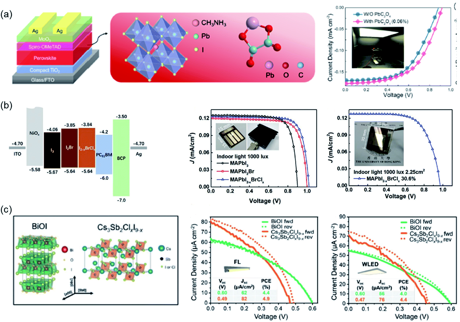 | ||
| Fig. 5 (a) Schematic diagram of PSCs fabricated with PbC2O4 doping and the J–V curves of with/without PbC2O4-based devices. Reproduced from ref. 201 with permission from the [American Chemical Society], copyright [2020]. (b) The bandgap of MAPbI3, MAPbI2Br, and MAPbI2−xBrClx perovskite and J–V curves of PSCs under indoor conditions. Reproduced from ref. 202 with permission from the [Wiley-VCH], copyright [2019]. (c) The crystal structure of BiOI and Cs3Sb2ClxI9−x and the J–V curves of the corresponding device under FL and WLED illuminations. Reproduced from ref. 205 with permission from the [Wiley-VCH], copyright [2020]. | ||
5.2 Interface engineering for PIPVs
In recent years, planar structure PSCs have attracted much attention owing to the simple fabrication process and low cost.208 However, interface conditions, such as interface contact, interface morphology, and interface defect, significantly affect the device performance of planar PSCs since these planar structure devices are very sensitive to the interfaces.209,210 Interfaces in PSCs (i.e., electron-transporting layer (ETL) or hole-transporting layer (HTL)/perovskite layer interface, front and back contact interfaces) strongly affect the charge extraction, recombination, and collection process.211 For high-performance PIPVs, the Shockley–Read–Hall (SRH) trap assisted recombination at the interface limits the improvement of the device performance. The non-radiative energy loss, energy-level mismatch, and optical losses at the interfaces are fatal to the performance of PIPVs under low light intensity indoor sources. Interface engineering is an effective strategy to improve the interface and interlayer properties to overcome interface loss. Notably, interface engineering can also largely improve cell stability.212In addition, interface engineering can effectively passivate defects on the perovskite film, modify the interface contact, and improve the carrier extraction/transport process with the goal of fabricating high-performance PIPVs. In 2018, Wang's group demonstrated high-performance MAPbI3-based IPVs with ionic liquid of (BMIM)BF4 as a modification layer, which can pave the interface contact (PCBM/perovskite layer) and passivate the trap states in the inverted, improving the electron transporting and extracting processes. The corresponding devices exhibit a recorded PCE of 35.20% under FL (1000 lux) (Fig. 6a).213 Recently, Wang's group reported a lycopene modification layer to fabricate (CsFAMA)Pb(I1−xBrx)3 films with fewer defects and better environmental stability, yielding an indoor PCE of 40.24% under LED (2700 K @ 1000 lux), which is the highest indoor efficiency among all PV systems till date.214 Considering the narrow spectrum of indoor light sources (200–700 nm), suitable bandgap (∼1.8 eV) of perovskite materials is more conducive to the fabrication of PIPVs with high performance and high Voc. Thus, a series of wide bandgap perovskite materials (e.g., CsPbBrI2 and (FA0.6MA0.4)0.9Cs0.1Pb(I0.6Br0.4)3) are considered for the fabrication of high-performance PIPVs. For example, Wang's group used (NH4)2C2O4·H2O to treat CsPbBrI2 (1.89 eV) film to make high quality perovskite film with micrometer-scale and low trap density (Fig. 6b). The optimal devices presented a best indoor PCE of 28.48% under an FL of 1000 lux.215 In 2020, Jen et al. also reported a simple strategy by applying PEACl, PEAI, and PEABr to reduce the energy loss and suppress the phase segregation of (FA0.6MA0.4)0.9Cs0.1Pb(I0.6Br0.4)3-based (1.75 eV) PIPVs (Fig. 6c). The optimized PIPVs by PEACl presented a PCE of 35.6% with Voc of 1.08 V under 1000 lux.216
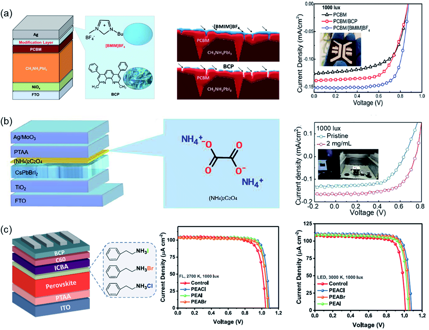 | ||
| Fig. 6 (a) Inverted structure PSCs, molecular structure of [BMIM]BF4 and BCP and the J–V curves. Reproduced from ref. 213 with permission from the [Wiley-VCH], copyright [2018]. (b) Device structure of CsPbBrI2 based PSCs, molecular structure of (NH4)2C2O4, and the J–V curves of devices with/without treatment. Reproduced from ref. 215 with permission from the [Elsevier], copyright [2020]. (c) Schematic diagram of PVCs, the chemical structures of PEACl, PEABr, PEAI, and the J–V curves of the device with/without treatment under CFL and LED irradiation. Reproduced from ref. 216 with permission from the [Elsevier], copyright [2020]. | ||
Similar to PSCs, PIPVs also consists of a perovskite layer sandwiched between two transporting layers (HTL and ETL) to form a multilayer structure. Considering the low light intensity of the indoor light source, the transporting layer with excellent properties can effectively reduce the charge non-radiative recombination loss at the interface and improve the extraction and transport process of carriers. On the one hand, the transporting materials for PSCs can also be considered for the fabrication of high-performance PIPVs. On the other hand, the different working environments of PIPVs and PSCs may also lead to the fact that charge transporting layers are not necessarily universal. For example, Tsoi et al. simulated different hole-transporting layers, such as mesoporous PPV (mPPV), carbon-based PPV (cPPV), and inverted PPV (iPPV) for PIPVs under an indoor environment (Fig. 7a). They found that the performance of mPPV-based indoor photovoltaic devices fabricated by Spiro-OMeTAD as the HTL were significantly better than other HTLs (PTAA, PEDOT:PSS and Poly-TPD), and the optimal device presented a maximum power exceeding 111 μW cm−2.217 In 2019, Samuel et al. demonstrated NiO nanoparticle based film (∼6 nm) as the HTL for MAPbI3-based PIPVs. The device presented a higher indoor PCE of 23% under FL illumination.218
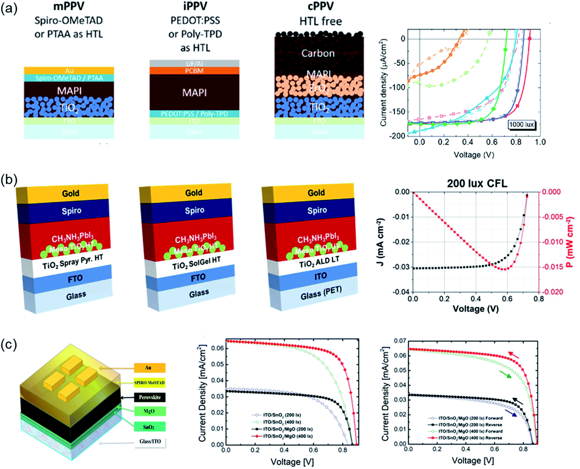 | ||
| Fig. 7 (a) The structural diagram of the three perovskite devices, and the J–V curve of the corresponding devices are at 1000 lux illumination. Reproduced from ref. 217 with permission from the [Wiley-VCH], copyright [2018]. (b) Schematic diagram of the structure of mesoporous TiO2 prepared by different methods and the J–V curve of the optimal device. Reproduced from ref. 223 with permission from the [Elsevier], copyright [2016]. (c) Schematic diagram of the device structure fabricated by SnO2 with MgO treatment and the J–V curves of the corresponding devices under different light conditions. Reproduced from ref. 227 with permission from the [Elsevier], copyright [2018]. | ||
In recent years, metal oxides (TiO2, InO3, ZnO, SnO2, etc.) have also been developed as ETL to fabricate high-performance inverted PSCs.219 Brown et al. explored the effect of TiO2 prepared by spray pyrolysis technique (SP), sol–gel process (SG) and atomic layer deposition (ALD) on the performance of MAPbI3-based PIPVs under FL illumination (Fig. 7b).220–223 The PIPVs fabricated by ALD TiO2 exhibited outstanding performance (PCE = 24%) under indoor light illumination (200 lux).223 Very recently, SnO2 with higher electron mobility, higher optical transparency, and wider bandgap has been developed to fabricate high-performance PIPVs.224–226 Brown et al. introduced a thin layer of MgO over the SnO2 to reduce the charge recombination at the interface (SnO2/perovskite layer) and improve the performance of PIPVs (Fig. 7c). The SnO2/MgO based PIPVs showed better power density values of 20.2 μW cm−2 (200 lux) and 41.6 μW cm−2 (400 lux).227 With the rapid development of material technology, we believe that more excellent charge-transporting materials will be designed and developed for the preparation of high-performance PIPVs.
6. Conclusion and perspectives
Under the background of the rapid development of IoTs and the gap in the demand for IPVs with hundreds of millions of markets, OPVs, DSSCs, and PIPVs have ushered in developing opportunities. Notably, the IPVs/PIPVs can not only be used in small devices such as wearable electronics, but also can be used as the main energy supply in some special situations (as BIPV) or under conditions of extensive coverage. Its maintenance cost will also be much lower than that of outdoor photovoltaics due to its milder operating environment. Furthermore, thin-film PVs represented by OPVs and DSSCs will occupy a dominant position in the current market due to their excellent performance and low cost. Nevertheless, PIPVs will dominate the market in the near future owing to their advantages of high efficiency, low cost, large area, and high defect tolerance. The development trend of PIPVs is also like other IPVs, tending to be a large area, low cost, high stability, and flexible fabrication. Thus, this review summarizes the cost, performance, merits, and future development trends of various types IPVs, especially programing the development trend of PIPVs, and summarizes the strategies for high-performance PIPV. We believe that the fabrication and development of high-performance PIPVs should follow the following parts:(A) Using composition engineering to adjust the bandgap and quality of perovskite films by optimizing the bandgap to 1.8–1.95 eV that fits the indoor light source.
(B) Using interface engineering to optimize crystallinity and passivate defects of perovskite films to reduce carrier non-recombination loss. Meanwhile, it is also important to optimize the transport layer material and minimize the recombination of the interfaces and the electrodes.
(C) Using high mobility, high flatness, and low-cost transporting materials to improve the extraction and transport process of carriers.
(D) Using ITO-free flexible substrates to fabricate high-performance PIPVs is more conducive to the advancement of their commercialization process due to their good stretch and flexibility.
(E) Using mature encapsulation techniques to improve the device lifetime.
Notably, considering the use of PIPVs devices in IoTs, the reduction in the use of the toxic element Pb (replaced by Sn, Rb, etc.) is often accompanied by a reduction in device performance. In addition, even considering the relatively mild indoor environment, the device lifetime of PIPV is still not enough to support its industrial development. It is undeniable that PIPV still has the potential to guide the IPVs in the future, owing to their excellent indoor performance.
Author contributions
K. L. W. collect reference, organize images and write manuscripts; Y. H. Z. modify the manuscript and participate in discussions; all the authors discussed the results and commented on the manuscript. Y. H. L. and Z.-K. W. supervised the project.Conflicts of interest
There are no conflicts to declare.Acknowledgements
The authors acknowledge financial support from the National Natural Science Foundation of China (No. 62075148, 52073197) and the Natural Science Foundation of Jiangsu Province (No. BK20201413). This project was also funded by the Collaborative Innovation Center of Suzhou Nano Science and Technology, and by the “111” Project of the State Administration of Foreign Experts Affairs of China.Notes and references
- The Internet of Things, ed. D. Giusto, A. Iera, G. Morabito and L. Atzori, Springer, 2010, ISBN: 978-1-4419-1673-0 Search PubMed.
- H. Jin, T.-P. Huynh and H. Haick, Nano Lett., 2016, 16, 4194–4202 CrossRef CAS PubMed.
- M. Xie, K. Hisano, M. Zhu, T. Toyoshi, M. Pan, S. Okada, O. Tsutsumi, S. Kawamura and C. Bowen, Adv. Mater. Technol., 2019, 4, 1800626 CrossRef.
- E. Ahmed, I. Yaqoob, I. A. T. Hashem, I. Khan, A. I. A. Ahmed, M. Imran and A. V. Vasilakos, Computer Networks, 2017, 129, 459–471 CrossRef.
- S. Li, L. Da Xu and S. Zhao, Information Systems Frontiers, 2015, 17, 243–259 CrossRef.
- I. Mathews, S. N. Kantareddy, T. Buonassisi and I. M. Peters, Joule, 2019, 3, 1415–1426 CrossRef CAS.
- Y. Cui, Y. Wang, J. Bergqvist, H. Yao, Y. Xu, B. Gao and J. Hou, Nat. Energy, 2019, 4, 768–775 CrossRef CAS.
- M. Freitag, J. Teuscher, Y. Saygili, X. Zhang, F. Giordano, P. Liska and A. Hagfeldt, Nat. Photonics, 2017, 11, 372–378 CrossRef CAS.
- J. K. W. Ho, H. Yin and S. K. So, J. Mater. Chem. A, 2020, 8, 1717–1723 RSC.
- I. Repins, M. A. Contreras, B. Egaas, C. DeHart, J. Scharf, C. L. Perkins, B. To and R. Noufi, Photovoltaics, 2008, 16, 235–239 CrossRef CAS.
- K. L. Chopra, P. D. Paulson and V. Dutta, Prog. Photovoltaics Res. Appl., 2004, 12, 69–92 CrossRef CAS.
- D. Song, M. Li, Y. Li, X. Zhao, B. Jiang and Y. Jiang, ACS Appl. Mater. Interfaces, 2014, 6, 10 Search PubMed.
- M. Freitag, J. Teuscher, Y. Saygili, X. Zhang, F. Giordano, P. Liska, J. Hua, S. M. Zakeeruddin, J.-E. Moser, M. Gratzel and A. Hagfeldt, Nat. Photonics, 2017, 11, 372 CrossRef CAS.
- S. Mathew, A. Yella, P. Gao, R. Humphry-Baker, B. F. E. Curchod, N. Ashari-Astani, I. Tavernelli, U. Rothlisberger, M. K. Nazeeruddein and M. Gratzel, Nat. Chem., 2014, 6, 242 CrossRef CAS PubMed.
- N. Gasparini, A. Salleo, I. McCulloch and D. Bara, Nat. Rev. Mater., 2019, 4, 229 CrossRef.
- J. Zhao, Y. Li, G. Yang, K. Jiang, H. Lin, H. Ade, W. Ma and H. Yan, Nat. Energy, 2016, 1, 15027 CrossRef CAS.
- J. Bisquert and E. J. Juarez-Perez, J. Phys. Chem. Lett., 2019, 10, 5889 CrossRef CAS PubMed.
- M. Saliba, T. Matsui, K. Domanski, J.-Y. Seo, A. Ummadisingu, S. M. Zakeeruddin, J.-P. Correa-Baena, W. R. Tress, A. Abate, A. Hagfeldt and M. Grätzel, Science, 2016, 354, 206 CrossRef CAS PubMed.
- H. S. Ryu, S. Y. Park, T. H. Lee, J. Y. Kim and H. Y. Woo, Nanoscale, 2020, 12, 5792–5804 RSC.
- Z. L. Wang, Adv. Mater., 2012, 24, 279 CrossRef.
- Z. L. Wang and W. Wu, Angew. Chem., Int. Ed., 2012, 51, 11700–11721 CrossRef CAS PubMed.
- B. Minnaert and P. Veelaert, Thin Solid Films, 2011, 519, 7537–7540 CrossRef CAS.
- P. Yongqiang, B. Tao and H. Lingxia, Infrared and Laser Engineering, 2012, 41, 2484–2488 Search PubMed.
- A. S. Teran, J. Wong, W. Lim, G. Kim, Y. Lee, D. Blaauw and J. D. Phillips, IEEE Trans. Electron Devices, 2015, 62, 2170–2175 CAS.
- A. Abbas, A. Abdollahinia, A. G. Aberle, S. Adachi, J. Adams, J. G. J. Adams and D. Aiken, IEEE J. Photovoltaics, 2013, 3, 1465 Search PubMed.
- M. Li, F. Igbari, Z. K. Wang and L. S. Liao, Adv. Energy Mater., 2020, 10, 2000641 CrossRef CAS.
- G. Létay and A. Bett, Spectrum, 2001, 20, 25 Search PubMed.
- T. C. J. Yang, P. Fiala, Q. Jeangros and C. Ballif, Joule, 2018, 2, 1421–1436 CrossRef CAS.
- J. Kim, J. H. Jang, E. Choi, S. J. Shin, J. H. Kim, G. G. Jeon and N. Park, Cell Rep. Phys. Sci., 2020, 1, 100273 CrossRef.
- G. Lucarelli, F. Di Giacomo, V. Zardetto, M. Creatore and T. M. Brown, Nano Res., 2017, 10, 2130–2145 CrossRef CAS.
- K. Sharma, V. Sharma and S. S. Sharma, Nanoscale Res. Lett., 2018, 13, 1–46 CrossRef CAS PubMed.
- M. Freunek and L. M. Reindl, IEEE J. Photovoltaics, 2013, 3, 1464 Search PubMed.
- I. Mathews, P. J. King, F. Stafford and R. Frizzell, IEEE J. Photovoltaics, 2015, 6, 230–235 Search PubMed.
- H. S. Jung and N. G. Park, Small, 2015, 11, 10–25 CrossRef CAS PubMed.
- L. Meng, J. You and Y. Yang, Nat. Commun., 2018, 9, 1–4 CrossRef CAS PubMed.
- C. Zhao, W. Tian, Q. Sun, Z. Yin, J. Leng, S. Wang and S. Jin, J. Am. Chem. Soc., 2020, 142, 15091–15097 CrossRef CAS PubMed.
- A. Karmakar, M. S. Dodd, S. Agnihotri, E. Ravera and V. K. Michaelis, Chem. Mater., 2018, 30, 8280–8290 CrossRef CAS.
- N. J. Jeon, J. H. Noh, W. S. Yang, Y. C. Kim, S. Ryu, J. Seo and S. I. Seok, Nature, 2015, 517, 476–480 CrossRef CAS PubMed.
- F. C. Chen, Adv. Opt. Mater., 2019, 7, 1800662 CrossRef.
- J. L. Wu, F. C. Chen, M. K. Chuang and K. S. Tan, Energy Environ. Sci., 2011, 4, 3374–3378 RSC.
- G. Dennler, S. Bereznev, D. Fichou, K. Holl, D. Ilic, R. Koeppe and T. Wöhrle, Sol. Energy, 2007, 81, 947–957 CrossRef CAS.
- J. F. Randall and J. Jacot, Renewable Energy, 2003, 28, 1851–1864 CrossRef CAS.
- R. Santbergen, J. M. Goud, M. Zeman, J. A. M. van Roosmalen and R. J. C. van Zolingen, Sol. Energy Mater. Sol. Cells, 2010, 94, 715–723 CrossRef CAS.
- X. Ma, S. Bader and B. Oelmann, IEEE Sens. J., 2017, 17, 3884–3891 Search PubMed.
- I. Mathews, S. N. Kantareddy, T. Buonassisi and I. M. Peters, Joule, 2019, 3, 1415–1426 CrossRef CAS.
- G. Apostolou, Procedia Environ. Sci., 2017, 38, 905–912 CrossRef.
- L. K. Ma, Y. Chen, P. C. Y. Chow, G. Zhang, J. Huang, C. Ma, J. Zhang, H. Yin, A. M. Hong Cheung, K. S. Wong, S. K. So and H. Yan, Joule, 2020, 4, 1486–1500 CrossRef CAS.
- S. Castro-Hermosa, G. Lucarelli, M. Top, M. Fahland, J. Fahlteich and T. M. Brown, Cell Rep. Phys. Sci., 2020, 1, 100045 CrossRef.
- V. C. Y. Chen, W. H. Lee, S. Y. Hsiao, W. L. Tsai, L. Yang, H. L. Lin, H. J. Chou and H. W. Lin, J. Mater. Chem. A, 2019, 7, 3612–3617 RSC.
- K. Kawata, K. Tamaki and M. Kawaraya, J. Photopolym. Sci. Technol., 2015, 28, 415–417 CrossRef CAS.
- M. Fath, A. Mefoued, A. Messaoud and Y. Boukennous, Phys. Procedia, 2009, 2, 751 CrossRef.
- Amorphous Solar Panel, https://www.wsl-solar.com/Amorphous_Solar_Panel/, accessed April 2020.
- Thin-Film Solar Cells for Low and High Illumination, https://www.com/en/indoor-solar-cells, accessed April 2020.
- Indoor Solar Panels, https://www.powerfilmsolar.com/specialty-markets/indoor-solar-panels/, accessed April 2020.
- Ricoh Launches the World's First Solid-State Dye-Sensitized Solar Cell Modules, https://www.ricoh.com/release/2020/0204_1/, accessed April 2020.
- Indoor Dye Sensitized Solar Cells, https://gcell.com/dye-sensi-tized-solar-cells/advantages-of-dscc/indoor-dye-sensitize-solar-cells, accessed April 2020.
- BCC Research, Wireless sensors: technologies and global markets, BCC Research, 2016, https://www.bccresearch.com/market-research/instrumentation-and-sensors/wireless-sensors-technologies-report-ias019c.html Search PubMed.
- P. D. Moskowitz and V. M. Fthenakis, Sol. Cells, 1990, 29, 63–71 CrossRef CAS.
- A. Babayigit, A. Ethirajan, M. Muller and B. Conings, Nat. Mater., 2016, 15, 247–251 CrossRef CAS PubMed.
- A. Babayigit, D. Duy Thanh, A. Ethirajan, J. Manca, M. Muller, H. G. Boyen and B. Conings, Sci. Rep., 2016, 6, 1–11 CrossRef PubMed.
- J. d. C. Silva, J. J. P. C. Rodrigues, A. M. Alberti, P. Solic and A. L. L. Aquino, presented at 2nd Int. Multidisciplinary Conf. on Computer and Energy Science (SpliTech), XXXX, Split, Croatia, July 2017 Search PubMed.
- BCC Research, Global Markets, Technologies and Devices for Energy Harvesting: EGY097C, https://www.prnewswire.com/news-releases/global-markets-technologies-and-devices-for-energy-har-vesting-300677825.html, accessed December 2019 Search PubMed.
- D. M. Powell, R. Fu, K. Horowitz, P. A. Basore, M. Woodhouse and T. Buonassisi, Energy Environ. Sci., 2015, 8, 3395–3408 RSC.
- M. O. Reese, S. Glynn, M. D. Kempe, D. L. McGott, M. S. Dabney, T. M. Barnes, S. Booth, D. Feldman and N. M. Haegel, Nat. Energy, 2018, 3, 1002–1012 CrossRef CAS.
- L. Lin, S. Jain and M. AlIoTso, in 2018 IEEE International Solid-State Circuits Conference-(ISSCC), IEEE, 2018, pp. 44–46 Search PubMed.
- M. Schuß, C. A. Boano, M. Weber and K. Römer, in EWSN, 2017, pp. 54–65 Search PubMed.
- BCC Research, Global Markets, Technologies and Devices for Energy Harvesting: EGY097C, 2018, https://www.bccresearch.com/market-research/energy-and-resources/global-markets-technologies-and-devices-for-energy-harvesting-egy097c.html Search PubMed.
- Technology Platforms for the Internet of Things (IoTs), https://www.bccresearch.com/market-research/information-technology/technology-platforms-for-the-internet-of-things-IoTs.html, accessed April 2020.
- W. Shockley and H. J. Queisser, J. Appl. Phys., 1961, 32, 510–519 CrossRef CAS.
- A. S. Teran, J. Wong, W. Lim, G. Kim, Y. Lee, D. Blaauw and J. D. Phillips, IEEE Trans. Electron Devices, 2015, 62, 2170–2175 CAS.
- Y. Cui, H. Yao, T. Zhang, L. Hong, B. Gao, K. Xian, J. Qin and J. Hou, Adv. Mater., 2019, 31, 1904512 CrossRef CAS PubMed.
- J. Peng, L. Lu, H. Yang and T. Ma, Renewable Energy, 2015, 80, 316–323 CrossRef CAS.
- Y. Li, N. J. Grabham, S. P. Beeby and M. J. Tudor, Sol. Energy, 2015, 111, 21–29 CrossRef CAS.
- N. H. Reich, W. G. J. H. M. Van Sark, E. A. Alsema, R. W. Lof, R. E. I. Schropp, W. C. Sinke and W. C. Turkenburg, Sol. Energy Mater. Sol. Cells, 2009, 93, 1471–1481 CrossRef CAS.
- C. Y. Chen, Z. H. Jian, S. H. Huang, K. M. Lee, M. H. Kao, C. H. Shen, J. M. Shieh, C. L. Wang, C. W. Chang and B. Z. Lin, J. Phys. Chem. Lett., 2017, 8, 1824–1830 CrossRef CAS PubMed.
- Y. Hu, S. Si, A. Mei, Y. Rong, H. Liu, X. Li and H. Han, Sol. RRL, 2017, 1, 1600019 CrossRef.
- H. K. Lee, Z. Li, J. R. Durrant and W. C. Tsoi, Appl. Phys. Lett., 2016, 108, 253301 CrossRef.
- K. Yoshikawa, H. Kawasaki, W. Yoshida, T. Irie, K. Konishi, K. Nakano and K. Yamamoto, Nat. Energy, 2017, 2, 1–8 Search PubMed.
- M. Freunek, M. Freunek and L. M. Reindl, IEEE J. Photovoltaics, 2012, 3, 59–64 Search PubMed.
- V. Bahrami-Yekta and T. Tiedje, Opt. Express, 2018, 26, 28238–28248 CrossRef CAS PubMed.
- M. H. Kao, C. H. Shen, P. C. Yu, W. H. Huang, Y. L. Chueh and J. M. Shieh, Sci. Rep., 2017, 7, 1–8 CrossRef CAS PubMed.
- M. Kasemann, K. Rühle, K. M. Gad and S. W. Glunz, Photovoltaic energy harvesting for smart sensor systems, International Society for Optics and Photonics, 2013 Search PubMed.
- Q. Li, K. Shen, R. Yang, Y. Zhao, S. Lu, R. Wang, J. Dong and D. Wang, Sol. Energy, 2017, 157, 216–226 CrossRef CAS.
- V. Ramanathan, L. A. Russell, C. H. Liu and P. V. Meyers, Sol. Cells, 1990, 28, 129–133 CrossRef CAS.
- P. D. Antunez, D. M. Bishop, Y. Luo and R. Haight, Nat. Energy, 2017, 2, 884–890 CrossRef CAS.
- C. Yang, J. Qu and Z. Wu, Sol. Energy, 2021, 214, 542–550 CrossRef CAS.
- M. A. Green, Y. Hishikawa, E. D. Dunlop, D. H. Levi, J. Hohl-Ebinger and A. W. Y. Ho-Baillie, Prog. Photovoltaics Res. Appl., 2018, 26, 427–436 CrossRef.
- I. Mathews, P. J. King, F. Stafford and R. Frizzell, IEEE J. Photovoltaics, 2016, 6, 230–235 Search PubMed.
- I. Mathews, G. Kelly, P. J. King and R. Frizzell, 2014 IEEE 40th Photovoltaic Specialist Conference (PVSC), IEEE, 2014, vol. 40, pp. 0510–0513 Search PubMed.
- M. Zhang, L. Zhu, T. Hao, G. Zhou, C. Qiu, Z. Zhao and F. Liu, Adv. Mater., 2021, 2007177 CrossRef CAS PubMed.
- H. K. H. Lee, J. Wu, J. Barbé, S. M. Jain, S. Wood, E. M. Speller, Z. Li, F. A. Castro, J. R. Durrant and W. C. Tsoi, J. Mater. Chem. A, 2018, 6, 5618–5626 RSC.
- Y. Cao, Y. Liu, S. M. Zakeeruddin, A. Hagfeldt and M. Grätzel, Joule, 2018, 2, 1108–1117 CrossRef CAS.
- M. Freitag, J. Teuscher, Y. Saygili, X. Zhang, F. Giordano, P. Liska, J. Hua, S. M. Zakeeruddin, J. E. Moser and M. Grätzel, Nat. Photonics, 2017, 11, 372–378 CrossRef CAS.
- H. Michaels, M. Rinderle, R. Freitag, I. Benesperi, T. Edvinsson, R. Socher and M. Freitag, Chem. Sci., 2020, 11, 2895–2906 RSC.
- D. Zhang, M. Stojanovic, Y. Ren, Y. Cao, F. T. Eickemeyer, E. Socie and M. Grätzel, Nat. Commun., 2021, 12, 1–10 CAS.
- Z. Ding, R. Zhao, Y. Yu and J. Liu, J. Mater. Chem. A, 2019, 7, 26533–26539 RSC.
- S. N. Agbo, T. Merdzhanova, U. Rau and O. Astakhov, Sol. Energy Mater. Sol. Cells, 2017, 159, 427–434 CrossRef CAS.
- A. S. Teran, E. Moon, W. Lim, G. Kim, I. Lee, D. Blaauw and J. D. Phillips, IEEE Trans. Electron Devices, 2016, 63, 2820–2825 CAS.
- Y. Dai, H. Kum, M. A. Slocum, G. T. Nelson and S. M. Hubbard, presented in part at the IEEE 44th Photovoltaic Specialist Conference (PVSC) 2017 Search PubMed.
- M. H. Ann, J. Kim, M. Kim, G. Alosaimi, D. Kim, N. Y. Ha and J. H. Kim, Nano Energy, 2020, 68, 104321 CrossRef CAS.
- Y. Cao, Y. Liu, S. M. Zakeeruddin, A. Hagfeldt and M. Grätzel, Joule, 2018, 2, 1108–1117 CrossRef CAS.
- H. Yin, S. Chen, S. H. Cheung, H. W. Li, Y. Xie, S. W. Tsang and S. K. So, J. Mater. Chem. C, 2018, 6, 9111–9118 RSC.
- L. J. A. Koster, V. D. Mihailetchi, H. Xie and P. W. M. Blom, Appl. Phys. Lett., 2005, 87, 203502 CrossRef.
- Z. Li, G. Lakhwani, N. C. Greenham and C. R. McNeill, J. Appl. Phys., 2013, 114, 034502 CrossRef.
- A. K. K. Kyaw, D. H. Wang, V. Gupta, W. L. Leong, L. Ke, G. C. Bazan and A. J. Heeger, ACS Nano, 2013, 7, 4569 CrossRef CAS PubMed.
- L. J. A. Koster, V. D. Mihailetchi, R. Ramaker and P. W. M. Blom, Appl. Phys. Lett., 2005, 86, 123509 CrossRef.
- S. R. Cowan, A. Roy and A. J. Heeger, Phys. Rev. B: Condens. Matter Mater. Phys., 2010, 82, 245207 CrossRef.
- T. Kirchartz, F. Deledalle, P. S. Tuladhar, J. R. Durrant and J. Nelson, J. Phys. Chem. Lett., 2013, 4, 2371–2376 CrossRef CAS.
- Y. J. You, C. E. Song, Q. V. Hoang, Y. Kang, J. S. Goo, D. H. Ko, J. J. Lee, W. S. Shin and J. W. Shim, Adv. Funct. Mater., 2019, 29, 1901171 CrossRef.
- Y. Cui, Y. Wang, J. Bergqvist, H. Yao, Y. Xu, B. Gao, C. Yang, S. Zhang, O. Inganäs, F. Gao and J. Hou, Nat. Energy, 2019, 4, 768–775 CrossRef CAS.
- R. Steim, T. Ameri, P. Schilinsky, C. Waldauf, G. Dennler, M. Scharber and C. J. Brabec, Sol. Energy Mater. Sol. Cells, 2011, 95, 3256 CrossRef CAS.
- S. Mori, T. Gotanda, Y. Nakano, M. Saito, K. Todori and M. Hosoya, Jpn. J. Appl. Phys., 2015, 54, 071602 CrossRef.
- A. Venkateswararao, J. K. W. Ho, S. K. So, S. W. Liu and K. T. Wong, Mater. Sci. Eng., R, 2020, 139, 100517 CrossRef.
- Y. Cui, L. Hong, T. Zhang, H. Meng, H. Yan, F. Gao and J. Hou, Joule, 2021, 5, 1016–1023 CrossRef.
- Z. Song, C. L. McElvany, A. B. Phillips, I. Celik, P. W. Krantz, S. C. Watthage and M. J. Heben, Energy Environ. Sci., 2017, 10, 1297–1305 RSC.
- O. Haillant, Sol. Energy Mater. Sol. Cells, 2011, 95, 1284 CrossRef CAS.
- G. Grancini, C. Roldán-Carmona, I. Zimmermann, E. Mosconi, X. Lee, D. Martineau and M. K. Nazeeruddin, Nat. Commun., 2017, 8, 1–8 CrossRef PubMed.
- X. He, J. Chen, X. Ren, L. Zhang, Y. Liu, J. Feng and S. Liu, Adv. Mater., 2021, 2100770 CrossRef CAS PubMed.
- S. A. Gevorgyan, M. V. Madsen, B. Roth, M. Corazza, M. Hösel, R. R. Søndergaard and F. C. Krebs, Adv. Energy Mater., 2016, 6, 1501208 CrossRef.
- S. S. Shin, E. J. Yeom, W. S. Yang, S. Hur, M. G. Kim, J. Im and S. I. Seok, Science, 2017, 356, 167–171 CrossRef CAS PubMed.
- W. Li, W. Zhang, S. Van Reenen, R. J. Sutton, J. Fan, A. A. Haghighirad and H. J. Snaith, Energy Environ. Sci., 2016, 9, 490–498 RSC.
- S. Ito, S. Tanaka, K. Manabe and H. Nishino, J. Phys. Chem. C, 2014, 118, 16995–17000 CrossRef CAS.
- C. J. Mulligan, M. Wilson, G. Bryant, B. Vaughan, X. Zhou, W. J. Belcher and P. C. Dastoor, Sol. Energy Mater. Sol. Cells, 2014, 120, 9 CrossRef CAS.
- C. J. Mulligan, M. Wilson, G. Bryant, B. Vaughan, X. Zhou, W. J. Belcher and P. C. Dastoor, Sol. Energy Mater. Sol. Cells, 2014, 120, 9–17 CrossRef CAS.
- C. Mayousse, C. Celle, A. Fraczkiewicz and J.-P. Simonato, Nanoscale, 2015, 7, 2107–2115 RSC.
- D. S. Hecht, L. Hu and G. Irvin, Adv. Mater., 2011, 23, 1482–1513 CrossRef CAS PubMed.
- B. T. Camic, H. J. Shin, M. H. Aslan, F. Basarir and H. Choi, J. Colloid Interface Sci., 2018, 512, 158–164 CrossRef PubMed.
- S. Kim, H. Oh, G. Kang, I. K. Han, I. Jeong and M. Park, ACS Appl. Energy Mater., 2020, 3, 6995–7003 CrossRef CAS.
- J. Dagar, S. Castro-Hermosa, M. Gasbarri, A. L. Palma, L. Cina, F. Matteocci and T. M. Brown, Nano Res., 2018, 11, 2669–2681 CrossRef CAS.
- F. Qin, J. Tong, R. Ge, B. Luo, F. Jiang, T. Liu and Y. Zhou, J. Mater. Chem. A, 2016, 4, 14017–14024 RSC.
- K. K. Sears, M. Fievez, M. Gao, H. C. Weerasinghe, C. D. Easton and D. Vak, Sol. RRL, 2017, 1, 1700059 CrossRef.
- X. L. Ou, M. Xu, J. Feng and H. B. Sun, Sol. Energy Mater. Sol. Cells, 2016, 157, 660–665 CrossRef CAS.
- S. P. Cho, S. L. Na and S. S. Kim, Sol. Energy Mater. Sol. Cells, 2019, 196, 1–8 CrossRef CAS.
- T. Aernouts, P. Vanlaeke, W. Geens, J. Poortmans, P. Heremans, S. Borghs, R. Mertens, R. Andriessen and L. Leenders, Thin Solid Films, 2004, 22, 451–452 Search PubMed.
- G. Dennler, C. Lungenschmied, H. Neugebauer, N. S. Sariciftci and A. Labouret, J. Mater. Res., 2005, 20, 3224 CrossRef CAS.
- N. G. Park and K. Zhu, Nat. Rev. Mater., 2020, 5, 333–350 CrossRef CAS.
- NREL Chart, in, June 2019..
- H. J. Snaith, J. Phys. Chem. Lett., 2013, 4, 3623–3630 CrossRef CAS.
- B. A. Nejand, P. Nazari, S. Gharibzadeh, V. Ahmadi and A. Moshaii, Chem. Commun., 2017, 53, 747–750 RSC.
- H. Tang, S. He and C. Peng, Nanoscale Res. Lett., 2017, 12, 1–8 CrossRef CAS PubMed.
- L. Cai, L. Liang, J. Wu, B. Ding, L. Gao and B. Fan, J. Semicond., 2020, 38, 014006 CrossRef.
- S. Razza, S. Castro-Hermosa, A. Di Carlo and T. M. Brown, APL Mater., 2016, 4, 091508 CrossRef.
- J. Burschka, N. Pellet, S. J. Moon, R. Humphry-Baker, P. Gao, M. K. Nazeeruddin and M. Grätzel, Nature, 2013, 499, 316–319 CrossRef CAS PubMed.
- F. De Rossi, T. Pontecorvo and T. M. Brown, Appl. Energy, 2015, 156, 413–422 CrossRef.
- K. Sun, J. Chang, F. H. Isikgor, P. Li and J. Ouyang, Nanoscale, 2015, 7, 896–900 RSC.
- H. D. Pham, S. M. Jain, M. Li, Z. K. Wang, S. Manzhos, K. Feron and P. Sonar, Adv. Electron. Mater., 2020, 6, 1900884 CrossRef CAS.
- Y. W. Noh, I. S. Jin, K. S. Kim, S. H. Park and J. W. Jung, J. Mater. Chem. A, 2020, 8, 17163–17173 RSC.
- R. Cheacharoen, C. C. Boyd, G. F. Burkhard, T. Leijtens, J. A. Raiford, K. A. Bush and M. D. McGehee, Sustainable Energy Fuels, 2018, 2, 2398–2406 RSC.
- H. C. Weerasinghe, Y. Dkhissi, A. D. Scully, R. A. Caruso and Y. B. Cheng, Nano Energy, 2015, 18, 118–125 CrossRef CAS.
- A. Uddin, M. B. Upama, H. Yi and L. Duan, Coatings, 2019, 9, 65 CrossRef.
- C. B. Wang, F. D. Gu, Z. R. Zhao, H. X. Rao, Y. M. Qiu, Z. L. Cai, G. Zhan, X. Y. Li, B. X. Sun, X. Yu, B. Q. Zhao, Z. W. Liu, Z. Q. Bian and C. H. Huang, Adv. Mater., 2020, 32, 1907623 CrossRef CAS PubMed.
- J. P. Cao and Y. Feng, Energy Environ. Sci., 2021, 14, 1286–1325 RSC.
- H. Yao, F. Zhou, Z. Li, Z. Ci, L. Ding and Z. Jin, Adv. Sci., 2020, 7, 1903540 CrossRef CAS PubMed.
- B. Chen, X. Zheng, Y. Bai, N. P. Padture and J. Huang, Adv. Energy Mater., 2017, 7, 1602400 CrossRef.
- M. Anaya, G. Lozano, M. E. Calvo and H. Míguez, Joule, 2017, 1, 769–793 CrossRef CAS.
- T. C.-J. Yang, P. Fiala, Q. Jeangros and C. Ballif, Joule, 2018, 2, 1421–1436 CrossRef CAS.
- N. N. Lal, Y. Dkhissi, W. Li, Q. Hou, Y.-B. Cheng and U. Bach, Adv. Energy Mater., 2017, 7, 1602761 CrossRef.
- E. L. Unger, L. Kegelmann, K. Suchan, D. Sörell, L. Korte and S. Albrecht, J. Mater. Chem. A, 2017, 5, 11401–11409 RSC.
- Z. Wang, Z. Song, Y. Yan, S. Liu and D. Yang, Adv. Sci., 2019, 6, 1801704 CrossRef PubMed.
- Z. Song, C. Chen, C. Li, R. A. Awni, D. Zhao and Y. Yan, Semicond. Sci. Technol., 2019, 34, 093001 CrossRef CAS.
- A. Kojima, K. Teshima, Y. Shirai and T. Miyasaka, J. Am. Chem. Soc., 2009, 131, 6050–6051 CrossRef CAS PubMed.
- M. M. Lee, J. Teuscher, T. Miyasaka, T. N. Murakami and H. J. Snaith, Science, 2012, 338, 643–647 CrossRef CAS PubMed.
- G. Kieslich, S. Sun and A. K. Cheetham, Chem. Sci., 2015, 6, 3430–3433 RSC.
- M. Saliba, J. P. Correa-Baena, M. Grätzel, A. Hagfeldt and A. Abate, Angew. Chem., Int. Ed., 2018, 57, 2554–2569 CrossRef CAS PubMed.
- https://www.nrel.gov/pv/assets/pdfs/best-research-cell-efficiencies.20200218.pdf .
- M. A. Green, Nat. Energy, 2016, 1, 15015 CrossRef.
- C. C. Chueh, C. Z. Li and A. K. Y. Jen, Energy Environ. Sci., 2015, 8, 1160–1189 RSC.
- Y. Deng, X. Zheng, Y. Bai, Q. Wang, J. Zhao and J. Huang, Nat. Energy, 2018, 3, 560–566 CrossRef CAS.
- J. P. Correa-Baena, A. Abate, M. Saliba, W. Tress, T. J. Jacobsson, M. Gratzel and A. Hagfeldt, Energy Environ. Sci., 2017, 10, 710–727 RSC.
- J. Gong, S. B. Darling and F. You, Energy Environ. Sci., 2015, 8, 1953–1968 RSC.
- N. Espinosa, L. Serrano-Luján, A. Urbina and F. C. Krebs, Sol. Energy Mater. Sol. Cells, 2015, 137, 303–310 CrossRef CAS.
- I. Celik, Z. Song, A. J. Cimaroli, Y. Yan, M. J. Heben and D. Apul, Sol. Energy Mater. Sol. Cells, 2016, 156, 157–169 CrossRef CAS.
- K. P. Bhandari, J. M. Collier, R. J. Ellingson and D. S. Apul, Renewable Sustainable Energy Rev., 2015, 47, 133–141 CrossRef.
- M. Cai, Y. Wu, H. Chen, X. Yang, Y. Qiang and L. Han, Adv. Sci., 2017, 4, 1600269 CrossRef PubMed.
- N. L. Chang, A. W. Yi Ho-Baillie, P. A. Basore, T. L. Young, R. Evans and R. J. Egan, Prog. Photovoltaics, 2017, 25, 390–405 Search PubMed.
- Y. Chen, L. Zhang, Y. Zhang, H. Gao and H. Yan, RSC Adv., 2018, 8, 10489–10508 RSC.
- Q. Jiang, Z. Chu, P. Wang, X. Yang, H. Liu, Y. Wang, Z. Yin, J. Wu, X. Zhang and J. You, Adv. Mater., 2017, 29, 1703852 CrossRef PubMed.
- K. Hwang, Y. S. Jung, Y. J. Heo, F. H. Scholes, S. E. Watkins, J. Subbiah, D. J. Jones, D. Y. Kim and D. Vak, Adv. Mater., 2015, 27, 1241–1247 CrossRef CAS PubMed.
- J. G. Tait, S. Manghooli, W. Qiu, L. Rakocevic, L. Kootstra, M. Jaysankar, C. A. Massede la Huerta, U. W. Paetzold, R. Gehlhaar, D. Cheyns, P. Heremans and J. Poortmans, J. Mater. Chem. A, 2016, 4, 3792–3797 RSC.
- O. A. Basaran, H. Gao and P. P. Bhat, Annu. Rev. Fluid Mech., 2013, 45, 85–113 CrossRef.
- F. D. Giacomo, S. Shanmugam, H. Fledderus, B. J. Bruijnaers, W. J. Verhees, M. S. Dorenkamper, S. C. Veenstra, W. Qiu, R. Gehlhaar and T. Merckx, Sol. Energy Mater. Sol. Cells, 2018, 181, 53–59 CrossRef.
- Z. Liu, L. Qiu, E. J. J. Perez, Z. Hawash, T. Kim, Y. Jiang, Z. Wu, S. R. Raga, L. K. Ono, S. F. Liu and Y. Qi, Nat. Commun., 2018, 9, 3880 CrossRef PubMed.
- C. Zuo, D. Vak, D. Angmo, L. Ding and M. Gao, Nano Energy, 2018, 46, 185–192 CrossRef CAS.
- J. E. Kim, S. S. Kim, C. Zuo, M. Gao, D. Vak and D. Y. Kim, Adv. Funct. Mater., 2019, 29, 1809194 CrossRef.
- Y. Y. Kim, T. Y. Yang, R. Suhonen, M. Välimäki, T. Maaninen, A. Kemppainen, N. J. Jeon and J. Seo, Adv. Sci., 2019, 6, 1802094 CrossRef PubMed.
- W. W. Liu, T. H. Wu, M. C. Liu, W. J. Niu and Y. L. Chueh, Adv. Mater. Interfaces, 2019, 6, 1801758 CrossRef.
- Z. Cheng and J. Lin, CrystEngComm, 2010, 12, 2646 RSC.
- I. C. Smith, E. T. Hoke, D. Solis-Ibarra, M. D. McGehee and H. I. Karunadasa, Angew. Chem., Int. Ed., 2014, 53, 1 CrossRef.
- L. J. Zuo, Q. Chen, N. D. Marco, Y. T. Hsieh, H. J. Chen, P. Y. Sun, S. Y. Chang, H. X. Zhao, S. Q. Dong and Y. Yang, Nano Lett., 2017, 17, 269 CrossRef CAS PubMed.
- T. Miyasaka, A. Kulkarni, G. M. Kim, S. Öz and A. K. Jena, Adv. Energy Mater., 2020, 10, 1902500 CrossRef CAS.
- A. Abate, Joule, 2017, 1, 659–664 CrossRef CAS.
- A. Singh, P. T. Lai, A. Mohapatra, C. Y. Chen, H. W. Lin, Y. J. Lu and C. W. Chu, Chem. Eng. J., 2021, 419, 129424 CrossRef CAS.
- G. Kapil, T. Bessho, T. Maekawa, A. K. Baranwal, Y. Zhang, M. A. Kamarudin and S. Hayase, Adv. Energy Mater., 2021, 2101069 CrossRef CAS.
- C. Wang, Y. Zhang, F. Gu, Z. Zhao, H. Li, H. Jiang and Z. Liu, Matter, 2021, 4, 709–721 CrossRef CAS.
- W. F. Yang, J. J. Cao, C. Dong, M. Li, Q. S. Tian, Z. K. Wang and L. S. Liao, Appl. Phys. Lett., 2021, 118, 023501 CrossRef CAS.
- S. Y. Park, J. S. Park, B. J. Kim, H. Lee, A. Walsh, K. Zhu and H. S. Jung, Nature Sustainability, 2020, 3, 1044–1051 CrossRef.
- F. Terroso-Saenz, A. González-Vidal, A. P. Ramallo-González and A. F. Skarmeta, Future Gener. Comput. Syst., 2019, 92, 1066–1079 CrossRef.
- D. L. DiLaura, K. Houser, R. Mistrick and G. R. Steffy, The lighting handbook: reference and application, 2011 Search PubMed.
- B. Minnaert and P. Veelaert, Energies, 2014, 7, 1500 CrossRef.
- W. J. Yin, T. Shi and Y. Yan, Appl. Phys. Lett., 2014, 104, 063903 CrossRef.
- C. Dong, M. Li, Y. Zhang, K. L. Wang, S. Yuan, F. Igbari, Y. G. Yang, X. Y. Gao, Z. K. Wang and L. S. Liao, ACS Appl. Mater. Interfaces, 2019, 12, 836–843 CrossRef PubMed.
- R. Cheng, C. C. Chung, H. Zhang, F. Liu, W. T. Wang, Z. Zhou, S. Wang, A. B. Djurišić and S. P. Feng, Adv. Energy Mater., 2019, 9, 1901980 CrossRef CAS.
- M. J. Wu, C. C. Kuo, L. S. Jhuang, P. H. Chen, Y. F. Lai and F. C. Chen, Adv. Energy Mater., 2019, 9, 1901863 CrossRef CAS.
- J. W. Lim, H. Kwon, S. H. Kim, Y. J. You, J. S. Goo, D. H. Ko, H. J. Lee, D. Kim, I. Chung, T. G. Kim, D. H. Kim and J. W. Shim, Nano Energy, 2020, 75, 104984 CrossRef CAS.
- Y. Peng, T. N. Huq, J. Mei, L. Portilla, R. A. Jagt, L. G. Occhipinti, J. L. MacManus-Driscoll, R. L. Z. Hoye and V. Pecunia, Adv. Energy Mater., 2021, 11, 2002761 CrossRef CAS.
- E. Jokar, C. H. Chien, C. M. Tsai, A. Fathi and E. W. G. Diau, Adv. Mater., 2019, 31, 1804835 CrossRef PubMed.
- L. Serrano-Lujan, N. Espinosa, T. T. Larsen-Olsen, J. Abad, A. Urbina and F. C. Krebs, Adv. Energy Mater., 2015, 5, 1501119 CrossRef.
- Q. Hu, J. Wu, C. Jiang, T. Liu, X. Que, R. Zhu and Q. Gong, ACS Nano, 2014, 8, 10161 CrossRef CAS PubMed.
- P. Schulz, E. Edri, S. Kirmayer, G. Hodes, D. Cahen and A. Kahn, Energy Environ. Sci., 2014, 7, 1377 RSC.
- G. Yang, H. Tao, P. Qin, W. Ke and G. Fang, J. Mater. Chem. A, 2016, 4, 3970–3990 RSC.
- J. Shi, X. Xu, D. Li and Q. Meng, Small, 2015, 11, 2472 CrossRef CAS PubMed.
- C. C. Boyd, R. Cheacharoen, T. Leijtens and M. D. McGehee, Chem. Rev., 2018, 119, 3418 CrossRef PubMed.
- M. Li, C. Zhao, Z. K. Wang, C. C. Zhang, H. K. H. Lee, A. Pockett, J. Barbé, W. C. Tsoi, Y. G. Yang, M. J. Carnie, X. Y. Gao, W. X. Yang, J. R. Durrant, L. S. Liao and S. M. Jain, Adv. Energy Mater., 2018, 8, 1801509 CrossRef.
- C. Dong, X. M. Li, C. Ma, W. F. Yang, J. J. Cao, F. Igbari, Z. K. Wang and L. S. Liao, Adv. Funct. Mater., 2021, 31, 2011242 CrossRef CAS.
- K. L. Wang, X. M. Li, Y. H. Lou, M. Li and Z. K. Wang, Sci. Bull., 2021, 66, 347–353 CrossRef CAS.
- Z. Li, J. Zhang, S. F. Wu, X. Deng, F. Z. Li, D. J. Liu, C. C. Lee, F. Lin, D. Y. Lei, C. C. Chueh, Z. L. Zhu and A. K. Y. Jen, Nano Energy, 2020, 78, 105377 CrossRef CAS.
- H. K. H. Lee, J. Barbé, S. M. Meroni, T. Du, C. T. Lin, A. Pockett, J. Troughton, S. M. Jain, F. D. Rossi, J. Baker, M. J. Carnie, M. A. McLachlan, T. M. Watson, J. R. Durrant and W. C. Tsoi, Sol. RRL, 2019, 3, 1800207 CrossRef.
- L. K. Jagadamma, O. Blaszczyk, M. T. Sajjad, A. Ruseckas and I. D. Samuel, Sol. Energy Mater. Sol. Cells, 2019, 201, 110071 CrossRef CAS.
- W. Ke, G. Fang, Q. Liu, L. Xiong, P. Qin, H. Tao, J. Wang, H. Lei, B. Li, J. Wan, G. Yang and Y. Yan, J. Am. Chem. Soc., 2015, 137, 6730–6733 CrossRef CAS PubMed.
- J. Burschka, N. Pellet, S. J. Moon, R. Humphry-Baker, P. Gao, M. K. Nazeeruddin and M. Grätzel, Nature, 2013, 499, 316–319 CrossRef CAS PubMed.
- S. Razza, F. Di Giacomo, F. Matteocci, L. Cinà, A. L. Palma, S. Casaluci, P. Cameron, A. D'Epifanio, S. Licoccia, A. Reale, T. M. Brown and A. Di Carlo, J. Power Sources, 2015, 277, 286–291 CrossRef CAS.
- B. Conings, L. Baeten, T. Jacobs, R. Dera, J. D'Haen, J. Manca and H. G. Boyen, APL Mater., 2014, 2, 081505 CrossRef.
- F. Di Giacomo, V. Zardetto, G. Lucarelli, L. Cinà, A. Di Carlo, M. Creatore and T. M. Brown, Nano Energy, 2016, 30, 460–469 CrossRef CAS.
- P. Tiwana, P. Docampo, M. B. Johnston, H. J. Snaith and L. M. Herz, ACS Nano, 2011, 5, 5158–5166 CrossRef CAS PubMed.
- H. J. Snaith and C. Ducati, Nano Lett., 2010, 10, 1259–1265 CrossRef CAS PubMed.
- F. Di Giacomo, A. Fakharuddin, R. Jose and T. M. Brown, Energy Environ. Sci., 2016, 9, 3007–3035 RSC.
- J. Dagar, S. Castro-Hermosa, G. Lucarelli, F. Cacialli and T. M. Brown, Nano Energy, 2018, 49, 290–299 CrossRef CAS.
| This journal is © The Royal Society of Chemistry 2021 |