
 Open Access Article
 This Open Access Article is licensed under a Creative Commons Attribution-Non Commercial 3.0 Unported Licence
Interplay of structural dynamics and electronic effects in an engineered assembly of pentacene in a metal–organic framework†
Ritesh
Haldar
 a,
Mariana
Kozlowska
b,
Michael
Ganschow
c,
Samrat
Ghosh
d,
Marius
Jakoby
e,
Hongye
Chen
af,
Farhad
Ghalami
g,
Weiwei
Xie
g,
Shahriar
Heidrich
b,
Yusuke
Tsutsui
d,
Jan
Freudenberg
c,
Shu
Seki
d,
Ian A.
Howard
eh,
Bryce S.
Richards
eh,
Uwe H. F.
Bunz
*c,
Marcus
Elstner
g,
Wolfgang
Wenzel
b and
Christof
Wöll
*a
a,
Mariana
Kozlowska
b,
Michael
Ganschow
c,
Samrat
Ghosh
d,
Marius
Jakoby
e,
Hongye
Chen
af,
Farhad
Ghalami
g,
Weiwei
Xie
g,
Shahriar
Heidrich
b,
Yusuke
Tsutsui
d,
Jan
Freudenberg
c,
Shu
Seki
d,
Ian A.
Howard
eh,
Bryce S.
Richards
eh,
Uwe H. F.
Bunz
*c,
Marcus
Elstner
g,
Wolfgang
Wenzel
b and
Christof
Wöll
*a
aKarlsruhe Institute of Technology (KIT), Institute of Functional Interfaces (IFG), Hermann-von Helmholtz Platz-1, 76344, Eggenstein-Leopoldshafen, Germany. E-mail: christof.woell@kit.edu
bKarlsruhe Institute of Technology (KIT), Institute of Nanotechnology (INT), Hermann-von-Helmholtz Platz-1, 76344, Eggenstein-Leopoldshafen, Germany
cOrganisch-Chemisches Institut, Ruprecht-Karls-Universität, Im Neuenheimer Feld 270, 69120 Heidelberg, Germany. E-mail: uwe.bunz@uni-heidelberg.de
dDepartment of Molecular Engineering, Graduate School of Engineering, Kyoto University, Nishikyo-ku, Kyoto 615-8510, Japan
eKarlsruhe Institute of Technology (KIT), Institute of Microstructure Technology (IMT), Hermann von-Helmholtz Platz-1, 76344, Eggenstein-Leopoldshafen, Germany
fState Key Laboratory of Mechanics and Control of Mechanical Structures, Key Laboratory for Intelligent Nano Materials and Devices of Ministry of Education, Institute of Nano Science, Nanjing, China
gKarlsruhe Institute of Technology, Institute of Physical Chemistry (IPC), Institute of Biological Interfaces (IBG2), 76131, Karlsruhe, Germany
hKarlsruhe Institute of Technology (KIT), Light Technology Institute (LTI), Engesserstrasse 13, 76131, Karlsruhe, Germany
First published on 8th February 2021
Abstract
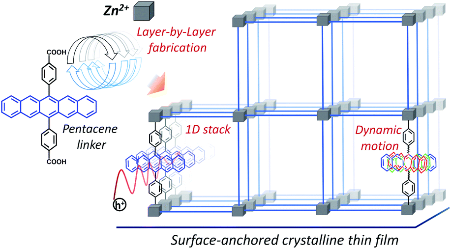
Charge carrier mobility is an important figure of merit to evaluate organic semiconductor (OSC) materials. In aggregated OSCs, this quantity is determined by inter-chromophoric electronic and vibrational coupling. These key parameters sensitively depend on structural properties, including the density of defects. We have employed a new type of crystalline assembly strategy to engineer the arrangement of the OSC pentacene in a structure not realized as crystals to date. Our approach is based on metal–organic frameworks (MOFs), in which suitably substituted pentacenes act as ditopic linkers and assemble into highly ordered π-stacks with long-range order. Layer-by-layer fabrication of the MOF yields arrays of electronically coupled pentacene chains, running parallel to the substrate surface. Detailed photophysical studies reveal strong, anisotropic inter-pentacene electronic coupling, leading to efficient charge delocalization. Despite a high degree of structural order and pronounced dispersion of the 1D-bands for the static arrangement, our experimental results demonstrate hopping-like charge transport with an activation energy of 64 meV dominating the band transport over a wide range of temperatures. A thorough combined quantum mechanical and molecular dynamics investigation identifies frustrated localized rotations of the pentacene cores as the reason for the breakdown of band transport and paves the way for a crystal engineering strategy of molecular OSCs that independently varies the arrangement of the molecular cores and their vibrational degrees of freedom.
Introduction
The determination of structure–property relationships in organic semiconductors (OSCs), which are promising materials for thin-film organic field-effect transistors,1–3 is often hampered by the lack of structural order. Aggregated OSC materials are very often amorphous or exhibit rather small structural coherence lengths, resulting in high defect densities. Charge carrier mobility, an important figure of merit of organic semiconductors, is not only affected by the electronic coupling between adjacent chromophores,4 but also by the coupling to vibrations within the molecular aggregates.5–7 These dynamic effects have emerged as a main bottleneck to improve the mobility in stacked organic semiconductors.8 Nevertheless, information on the interplay of these factors is scarce. In addition, rational optimization is hampered by the fact that the variations of the molecular core, aimed at the reduction of the amplitudes of the most important vibrations, also changes the crystal structure and the other relevant vibrational modes for the semiconducting performance. It would therefore be of interest to investigate structurally well-defined model systems where planar, aromatic molecules are packed into crystalline arrangements with a high degree of structural control and low defect density. This can offer independent control over the molecular arrangement and reduce the vibrational degrees of freedom of the system.9–12An interesting case is that of pentacene (Pn), an OSC with charge carrier mobilities as high as those of amorphous silicon, which features a highly rigid core. Although mobilities of bulk Pn single crystals are fairly large, it has been speculated that these values may be enhanced further when the relative orientations of the aromatic plane are modified. Variation of side-groups and growth conditions yields herringbone or cofacial (brick-wall, slipped or cofacial) stacks of the aromatic cores with variable charge carrier mobilities.13,14 Employing the existing methods of Pn film preparation, often polycrystalline films with the coexistence of more than one crystalline phase are obtained.15 As a result, establishing structure–property correlations is not straightforward. In particular structural defects hamper the determination of intrinsic properties. In the previous works, charge carrier mobilities in condensed phases of pentacene were observed to vary by one order of magnitude depending on preparation conditions (see Table S1†).
Here, we present a robust strategy to engineer the packing of OSCs into highly ordered columns with strong electronic coupling between the aromatic cores. The key first step of the approach is to equip the target OSC with two anchoring groups, so as to yield ditopic linkers. These modified OSCs are then coordinated to appropriate metal/metal-oxo nodes, to yield metal–organic frameworks (MOFs) or porous coordination polymers.16–18 MOFs exhibit a high degree of structural order and modularity.16–18 A number of strategies to control the crystalline order, orientation, and defect concentration have been developed.19,20 In the recent years, it has been possible to preconceive OSC arrangements for a large variety of applications, including optoelectronics.21–26 Originally developed for applications in gas storage and separation, MOF-based materials have found interest also with regard to other application fields, based on properties like large electrical conductivities27 of the order of 103 S m−1, room temperature charge carrier mobility28 as large as 220 cm2 V−1 s−1, and other interesting properties like thermal activated delayed fluorescence,29 emphasizing the emergent nature of MOF-based optoelectronic materials.30–33
In the present work, we demonstrate the potential of the MOF-based approach to create structurally-controlled 1D OSCs based on Pn. The ditopic linker required for MOF synthesis was fabricated by attaching two phenylcarboxylate groups to the Pn (Scheme 1 and Fig. S1†). While in principle the availability of such Pn-based linkers allows the realization of a multitude of different types of MOFs (e.g. by using so-called layered pillar structures34) we focused here on MOF-2,35 one of simplest realizations of a MOF using ditopic linkers. Note, that because the overall topology of MOF-2 is given by the bonding of the carboxylate groups to either Zn2+ or Cu2+ dimers, crystal structure prediction methods can be applied in a straightforward fashion.36
 | ||
| Scheme 1 Illustration of a pentacene (Pn)-based metal–organic framework thin film fabrication scheme in a layer-by-layer fashion, and the impact of linker-dynamics on the hole mobility. | ||
In this work, we have used a variant of MOF-2, in which the 6,13-substituted Pn-linker is connected to Zn-oxo-nodes (Scheme 1) to form a crystalline, structure containing 1D chains of Pn. Since the conventional, solvothermal synthesis of MOF-2 yields polycrystalline powders, not well suited for high-accuracy measurements of the mobility, we have used the SURMOF (surface-anchored MOF) approach37 to fabricate highly oriented MOF thin films. We demonstrate in the following that in SURMOF structure (Zn–Pn) the Pn units are arranged in a parallel fashion with high crystalline order. As evidenced by a thorough photophysical characterizations and a density functional theory (DFT) analysis, this molecular arrangement yields strong inter-Pn electronic coupling. Interestingly, instead of the expected band-like charge transport, the Zn–Pn SURMOFs exhibited an intrinsic hopping-like photogenerated charge (hole) carrier mobility of ∼0.03 cm2 V−1 s−1 at 300 K with an activation energy of ∼64 meV. In the context of a prevailing theory of charge transport, strong fluctuations of the intermolecular couplings often play a key role and strongly reduce the hypothetical, large mobility predicted for static arrangements.7 Our theoretical results confirmed that transport mechanism along the 1D Pn stacks is largely governed by dynamic contributions (illustrated in Scheme 1), arising from rotations of the Pn linkers around the 6,13-axis defined by the two metal-coordinating carboxylate groups. This frustrated rotation causes fluctuations of the inter-Pn electronic coupling and dynamic disorder, resulting in partial hole delocalization and charge transport mechanism at the borderline between the localized hopping and delocalized charge transport. With the insights from the detailed static and dynamic quantum-mechanical investigations, we identified key principles governing the charge carrier properties of such arrayed columns of OSC compounds.
Results and discussion
Here, our SURMOF approach assembled Pn-based linkers into arrayed 1D Pn-columns oriented parallel to the substrate. Such monolithic MOF thin films were deposited on functionalized substrates using a layer-by-layer (lbl) liquid-phase epitaxy (LPE) method.37 Using optimized synthesis conditions yield thin films of high optical quality;38 any opacity resulting from light scattered by domain boundaries or crystallites is almost completely absent. SURMOFs can be grown with variable thickness and reduced (compared to bulk synthesis methods) structural defects; these properties are beneficial for optical characterizations and device-based optoelectronic applications.39 The Zn–Pn SURMOFs used here were prepared by employing the lbl spin-coating method using ethanolic solutions of Zn-acetate and suitably designed Pn-linker. The latter was prepared in a two-step procedure starting from 6,13-dichloropentacene40 (unlike the previous methodology by Yanai and co-workers41) after Suzuki coupling with (4-(methoxycarbonyl)phenyl)boronic acid and subsequent hydrolysis under acidic conditions. The overall yield was 29% (see ESI for synthesis details, Fig. S1†). After fabrication of the Zn–Pn SURMOF, the crystalline framework was analyzed using out- and in-plane X-ray diffraction (XRD). The XRD patterns revealed the presence of a SURMOF-2 type structure42 with unit cell dimensions of a = b = 2.1 nm, c = 0.58 nm and continuous, quasi-1D rows of stacked pentacene cores along the [001] direction (c-axis), as illustrated in Fig. 1a and b. In Fig. 1c, we illustrate that with this specific stacking, the closest C–C distance among the Pn-linkers can be 0.38 nm, enabling strong π–π interactions (predicted by the plane-wave density functional theory (DFT) upon optimization of the Zn–Pn unit cell; see ESI, Fig. S2–S4†).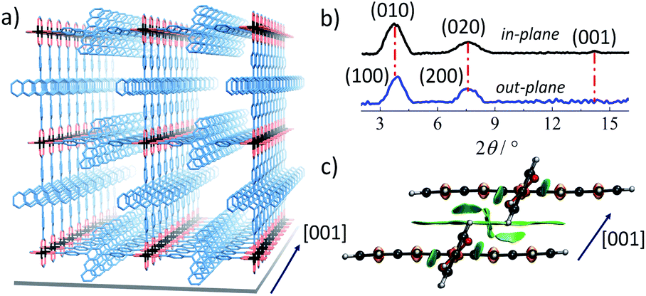 | ||
| Fig. 1 (a) 1D arrays of pentacene (in blue) in the predicted SURMOF-2 structure of Zn–Pn; (b) out-of-plane (blue) and in-plane (black) XRDs of Zn–Pn, red-dotted lines are guides to the eye; (c) visualization of the intra/intermolecular stacking interactions between the Pn fragments of Zn–Pn (noncovalent interaction surface of isovalue 0.3 a.u. is marked in green and red). | ||
The close proximity of the Pn linkers results in a strong inter-Pn electronic coupling, as confirmed by the absorption and emission spectra of Zn–Pn. Pn in the solvated state (20 μM in ethanol) exhibited well-resolved vibronic feature in the absorption spectrum with maximum ∼2.1 eV (Fig. 2a). In contrast, after aggregation into the Zn–Pn thin film, we observed that the absorption maximum is shifted to lower energy by 50 meV and that the vibronic intensities changed substantially in comparison to that of the solvated Pn linker. These experimental observations were consistent with theoretical results. The calculated electronic spectra of the Pn-linker assembly (using CAM-B3LYP functional with def2-TZVP basis set) showed the change of the orbital energies and transition orbital contributions upon excitation (Fig. S5 and S6†). On the basis of these observations, we predict an aggregation-induced lowering of the singlet–singlet transition energy by 35 meV in the Zn–Pn assembly compared to its free state (Fig. S5,† calculated spectra). For a comparison, note that the calculated singlet–singlet transition energy of the pristine Pn-herringbone (bulk form of pentacene crystals) type packing appeared at higher energy and featured different vibronic intensities, compared to that of the 1D assembly in Zn–Pn (Fig. S5†).
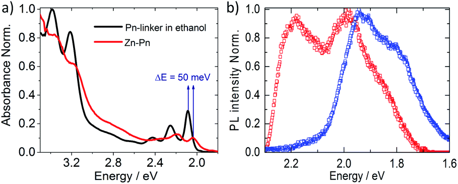 | ||
| Fig. 2 (a) Absorption spectra of Pn-linker in solvated state (20 μM in ethanol) and in SURMOF-2; (b) PL spectra of Zn–Pn thin film showing two excited states, monomer (red) and excimer (blue). | ||
The described modification of the electronic transition energy in Zn–Pn is a result of the slipped parallel stacking. This was also supported by photoluminescence (PL) spectra. Upon excitation of Zn–Pn at 3.49 eV we observed two distinct emissive states with maxima at 2.19 eV (life-time ∼ 1 ns) and 1.93 eV (life-time ∼ 4 ns), suggesting monomer and excimer like features (Fig. 2b and S7†).
Considering the fact that the Pn linkers are within the 1D columns running along the [001] direction (parallel to the substrate), we expected that the electronic coupling of the aromatic cores should lead to a strongly anisotropic delocalization of charge. To study the consequences of such a delocalization, we investigated the photoconductivity of the Zn–Pn thin film at different temperatures. We have used flash-photolysis time-resolved microwave conductivity (FP-TRMC) system coupled with transient absorption spectroscopy (TAS) to estimate the mobility at 300 K (see Experimental section in the ESI†). In this regard, monolithic Zn–Pn thin film having high light penetration depth and homogeneity possesses a clear advantage in comparison to the conventional MOF powders. At 300 K upon excitation at 3.49 eV, Zn–Pn exhibited a transient photoconductivity (φΣμ), where φ and Σμ correspond to the charge-carrier generation quantum yields and the charge-carrier mobilities, respectively (Fig. 3). To estimate the charge carrier (Pn cation) generation efficiency (φ) of the Zn–Pn, transient absorption spectra at excitation 3.49 eV was measured (Fig. S8 and S9†). Fig. S9† illustrates the photobleaching of the Pn cation radical, and the estimated charge carrier efficiency (φ) amounted to 1.02 × 10⁻³ (at 300 K). Using these parameters, the intrinsic photogenerated charge (hole) carrier mobility is estimated to be 0.03 cm2 V−1 s−1 at 300 K. This value compares well with other MOF-based semiconductors (porphyrin ∼ 0.001–0.004 cm2 V−1 s−1,24 tetrathiafulvalene ∼ 0.2 cm2 V−1 s−1 (ref. 43)). These data demonstrated that the packing of Pn in MOF–Pn is a robust structure engineering strategy, which leads to stacks with strong coupling with high static mobilities and which offers sufficient variability of tuning the precise arrangement without affecting the overall stacking motif. To get an insight of the hole mobility pathway, we have carried out temperature dependent FP-TRMC (Fig. S10 and S11†). A decrease in photoconductivity was observed upon lowering the temperature, suggest a thermally activated process with an activation energy of ∼64 meV, clearly suggesting a hopping like charge transport in Zn–Pn (Fig. 3, S10 and S11†).
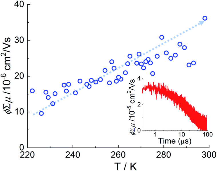 | ||
| Fig. 3 Temperature dependent FP-TRMC plot for Zn–Pn thin film; inset: FP-TRMC profile of Zn–Pn SURMOF-2 upon photoexcitation at 355 nm, at 300 K. The photon density is 8.9 × 10¹⁵ photons per cm2. | ||
The presence of hopping transport is somewhat surprising. Considering the well-defined, close proximity packing of Pn in the Zn–Pn SURMOF, we expected facile band-like transport, as also indicated by a first set of static DFT calculations (see ESI, Fig. S12†). Since the high structural order of the Zn–Pn SURMOFs allowed to exclude extrinsic contributions from contaminations or defects, we felt that the dominance of hopping over band transport effects must be an intrinsic property of this system. In order to unravel the reasons for this surprising finding, we subjected the system to a more thorough theoretical analysis by employing the semiclassical Marcus theory of hopping charge transport.44–46 The electronic coupling elements between the Pn linkers were calculated using the ab initio Quantum Patch method (with B3LYP/def2-TZVP) based on molecular orbitals47–49 using the periodic SURMOF structure optimized with PBE+D3 in VASP50 (version 5.4.1). The electronic coupling of the highest occupied molecular orbitals (HOMO) in the Pn stacking direction (i.e. along [001], as shown in Fig. 1) was found to be of 34 meV, resulting in the hole mobility of ∼2.13 cm2 V−1 s−1 at 300 K (along other directions, coupling is weak and consequently mobility is very low). In the case of mobility >1 cm2 V−1 s−1, time scale of charge transport and relaxation process are similar51–53 and hence hopping transport alone cannot be adequate to explain the observed mobility in the Zn–Pn.
To address the transport mechanism, we applied a multiscale computational scheme, which simulates the direct propagation of charge carriers using the time-dependent Schrödinger equation, coupled to the classical motion of nuclei.54,55 In agreement with the results from Marcus theory, we find a mobility of 1.98 cm2 V−1 s−1, although the charge is delocalized over 2 Pn linkers, on average (Table S4†). The mobility increases steadily from 150 to 350 K (Fig. S16†), in accordance with the experimental finding, which is a feature of Marcus-like transport. Evidently, in Zn–Pn the charge transport mechanism is at the borderline between the localized hopping and delocalized charge transport, and the transition is depending on the temperature/localized dynamics.
Clearly, by only considering static contributions, we cannot explain the presence of hopping-like charge transport in this highly ordered system. Consequently, we explicitly considered the dynamic motion of the aromatic rings of Pn linker originating from frustrated rotations around the center axis. The occurrence of dynamic phenomena in MOF structures is common,56–59 but has not yet been discussed in connection with charge transport phenomena. We applied a molecular dynamics simulation to understand the local, structural dynamics in Zn–Pn. We observed that molecular motions are prominent in Zn–Pn, as illustrated in Fig. 4a and b. In comparison, a pristine pentacene crystal (without having metal anchoring Ph–COOH group, see ESI†) is more rigid (Fig. S14 and S15†). The highly dynamic localized motion of the Pn linker in Zn–Pn yields strong fluctuations of the electronic coupling (standard deviation of 27 meV, see Fig. 4b) of the order of the average coupling of 30 meV, which results in more localized states. As a consequence, in these 1D stacks band-transport is suppressed (partial charge carrier delocalization over two molecules) and the motion of charge carriers is dominated by hopping. The coherence factor (a measure for the impact of the nuclear fluctuations on the transport)60 for the Zn–Pn was estimated to be 0.55, while the corresponding value for bulk pentacene amounts to 0.85. Therefore, the local structural dynamics in the 1D chains of Zn–Pn contribute decisively to the observed charge transport.
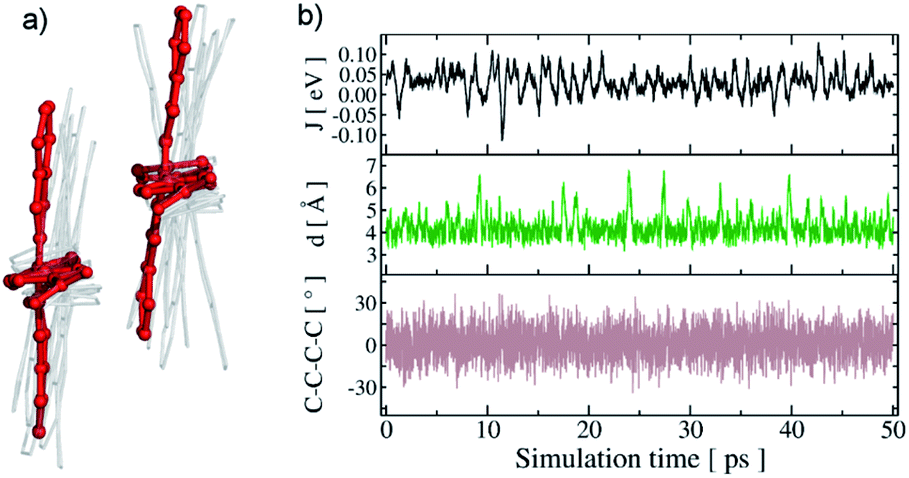 | ||
| Fig. 4 (a) Overlay of the Pn-linker nuclear displacements in the SURMOF from molecular dynamics simulations at 300 K, (b) change of the electronic coupling between the Pn-linkers in Zn–Pn (upper panel); change of the closest intermolecular C–C distance (middle panel) and out-of-plane distortions of the pentacene fragment of the linker (bottom panel). | ||
Conclusions
A new, MOF-based approach has been introduced to allow crystal engineering of columnar arrays of OSC compounds. In a first, pentacene-based example, a thorough photophysical characterization and subsequent temperature dependent charge carrier mobility experiments revealed, surprisingly, a hopping-like transport, with an activation energy of ∼64 meV. A detailed study based on both, experiment and theory, has allowed identifying the separate contributions to charge carrier mobility and confirmed that the fluctuations of the organic molecules in the context of their crystal packing are a parameter of key importance. The intrinsic rotational motion of the (rigid) pentacene linkers, strongly suppresses charge delocalization along the π-stacked pentacene, yielding to delocalization over two neighboring linkers, suggesting the charge transport mechanism in this MOF at the borderline between the localized hopping (dominant at room temperature) and delocalized charge transport. Our data shows that in this, first, pentacene-based example of a MOF-based OSC material, the relative fluctuations result in a coherence parameter of 0.55, reflecting significantly larger dynamical fluctuations of the electronic coupling than prevalent in conventional high mobility organic semiconductors. Since these fluctuations do not originate from the rigid pentacene core, but are mostly a result of the flexible anchoring of the linker in the molecular framework, this MOF-based approach thus opens up the perspective of modifying the mechanical coupling of the OSC moieties (e.g. by introducing stiff side groups) independently of the electronic coupling of the OSC cores. As we have shown in the prior work,36 modification of the non-functional part of the MOF-linker permits in silico crystal engineering of the structural properties of MOFs. This will allow reducing the fluctuations of the MOF framework, while at the same time maintaining the favourable stacking of the OSC cores, thus resulting in a substantial enhancement of charge carrier mobilities.Author contributions
R. H., U. H. F. B. and C. W. designed the project; R. H., H. C., did the SURMOF synthesis and photophysical characterizations; M. G., J. F. did the linker synthesis with guidance from U. H. F. B.; S. G., M. J., Y. T. did the mobility measurement experiments with guidance from S. S., I. A. H., B. S. R.; M. K., F. G., W. X., S. H. did the computational studies with guidance from W. W., M. E.; R. H., M. K., W. W., C. W. drafted the manuscript with inputs from all the authors.Conflicts of interest
There are no conflicts to declare.Acknowledgements
This research was funded by the Deutsche Forschungsgemeinschaft (DFG, German Research Foundation) under the Germany Excellence Strategy via the Excellence Cluster 3D Matter Made to Order (grant no. EXC-2082/1-390761711), Thrusts A1 and A2. We acknowledge the support by the DFG through SFB 1249 “N-Heteropolycycles as Functional Materials” (B02) and the Virtual Materials Design initiative (Virtmat) funded by KIT. M. K. acknowledges funding by the Ministry of Science, Research and Art of Baden-Württemberg (Germany) under the Brigitte-Schlieben-Lange-Programm. The authors acknowledge support by the state of Baden-Württemberg through bwHPC and the German Research Foundation (DFG) through grant no. INST 40/575-1 FUGG (JUSTUS 2 cluster). This work was performed on the supercomputer ForHLR II, funded by the Ministry of Science, Research and the Arts Baden-Württemberg and by the Federal Ministry of Education and Research. S. G., S. S., and Y. T. acknowledge the Japan Society for the Promotion of Science (JSPS) for Grant-in-Aid for Scientific Research (19F19044, 20H05862, and 19K23651).Notes and references
- T. Jousselin-Oba, M. Mamada, J. Marrot, A. Maignan, C. Adachi, A. Yassar and M. Frigoli, Excellent Semiconductors Based on Tetracenotetracene and Pentacenopentacene: From Stable Closed-Shell to Singlet Open-Shell, J. Am. Chem. Soc., 2019, 141, 9373–9381 CrossRef.
- A. J. Petty, Q. Ai, J. C. Sorli, H. F. Haneef, G. E. Purdum, A. Boehm, D. B. Granger, K. Gu, C. P. L. Rubinger, S. R. Parkin, K. R. Graham, O. D. Jurchescu, Y.-L. Loo, C. Risko and J. E. Anthony, Computationally aided design of a high-performance organic semiconductor: the development of a universal crystal engineering core, Chem. Sci., 2019, 10, 10543–10549 RSC.
- H. Usta, D. Kim, R. Ozdemir, Y. Zorlu, S. Kim, M. C. Ruiz Delgado, A. Harbuzaru, S. Kim, G. Demirel, J. Hong, Y.-G. Ha, K. Cho, A. Facchetti and M.-G. Kim, High Electron Mobility in [1]Benzothieno[3,2-b][1]benzothiophene-Based Field-Effect Transistors: Toward n-Type BTBTs, Chem. Mater., 2019, 31, 5254–5263 CrossRef CAS.
- K. M. Felter, V. M. Caselli, D. D. Günbaş, T. J. Savenije and F. C. Grozema, Interplay between Charge Carrier Mobility, Exciton Diffusion, Crystal Packing, and Charge Separation in Perylene Diimide-Based Heterojunctions, ACS Appl. Energy Mater., 2019, 2, 8010–8021 CrossRef CAS.
- T. Kubo, R. Häusermann, J. Tsurumi, J. Soeda, Y. Okada, Y. Yamashita, N. Akamatsu, A. Shishido, C. Mitsui, T. Okamoto, S. Yanagisawa, H. Matsui and J. Takeya, Suppressing molecular vibrations in organic semiconductors by inducing strain, Nat. Commun., 2016, 7, 11156 CrossRef CAS.
- M. Ando, M. Yoneya, T. B. Kehoe, H. Ishii, T. Minakata, M. Kawasaki, C. M. Duffy, R. Phillips and H. Sirringhaus, Disorder and localization dynamics in polymorphs of the molecular semiconductor pentacene probed by in situ micro-Raman spectroscopy and molecular dynamics simulations, Phys. Rev. Mater., 2019, 3, 025601 CrossRef CAS.
- S. Fratini, S. Ciuchi, D. Mayou, G. T. de Laissardière and A. Troisi, A map of high-mobility molecular semiconductors, Nat. Mater., 2017, 16, 998–1002 CrossRef CAS.
- S. Illig, A. S. Eggeman, A. Troisi, L. Jiang, C. Warwick, M. Nikolka, G. Schweicher, S. G. Yeates, Y. Henri Geerts, J. E. Anthony and H. Sirringhaus, Reducing dynamic disorder in small-molecule organic semiconductors by suppressing large-amplitude thermal motions, Nat. Commun., 2016, 7, 10736 CrossRef CAS.
- K. A. McGarry, W. Xie, C. Sutton, C. Risko, Y. Wu, V. G. Young, J.-L. Brédas, C. D. Frisbie and C. J. Douglas, Rubrene-Based Single-Crystal Organic Semiconductors: Synthesis, Electronic Structure, and Charge-Transport Properties, Chem. Mater., 2013, 25, 2254–2263 CrossRef CAS.
- B. Zhang, H. Soleimaninejad, D. J. Jones, J. M. White, K. P. Ghiggino, T. A. Smith and W. W. H. Wong, Highly Fluorescent Molecularly Insulated Perylene Diimides: Effect of Concentration on Photophysical Properties, Chem. Mater., 2017, 29, 8395–8403 CrossRef CAS.
- D. H. Arias, J. L. Ryerson, J. D. Cook, N. H. Damrauer and J. C. Johnson, Polymorphism influences singlet fission rates in tetracene thin films, Chem. Sci., 2016, 7, 1185–1191 RSC.
- X. Wang, T. Garcia, S. Monaco, B. Schatschneider and N. Marom, Effect of crystal packing on the excitonic properties of rubrene polymorphs, CrystEngComm, 2016, 18, 7353–7362 RSC.
- J. E. Anthony, J. S. Brooks, D. L. Eaton and S. R. Parkin, Functionalized Pentacene: Improved Electronic Properties from Control of Solid-State Order, J. Am. Chem. Soc., 2001, 123, 9482–9483 CrossRef CAS.
- J. E. Anthony, D. L. Eaton and S. R. Parkin, A Road Map to Stable, Soluble, Easily Crystallized Pentacene Derivatives, Org. Lett., 2002, 4, 15–18 CrossRef CAS.
- S. Lukas, S. Söhnchen, G. Witte and C. Wöll, Epitaxial Growth of Pentacene Films on Metal Surfaces, ChemPhysChem, 2004, 5, 266–270 CrossRef CAS.
- S. Kitagawa, R. Kitaura and S.-i. Noro, Functional Porous Coordination Polymers, Angew. Chem., Int. Ed., 2004, 43, 2334–2375 CrossRef CAS.
- H. Furukawa, K. E. Cordova, M. O'Keeffe and O. M. Yaghi, The Chemistry and Applications of Metal–Organic Frameworks, Science, 2013, 341, 1230444 CrossRef.
- S. Horike, S. Shimomura and S. Kitagawa, Soft porous crystals, Nat. Chem., 2009, 1, 695–704 CrossRef CAS.
- Z. Wang, S. Henke, M. Paulus, A. Welle, Z. Fan, K. Rodewald, B. Rieger and R. A. Fischer, Defect Creation in Surface-Mounted Metal–Organic Framework Thin Films, ACS Appl. Mater. Interfaces, 2020, 12, 2655–2661 CrossRef CAS.
- K. Müller, K. Fink, L. Schöttner, M. Koenig, L. Heinke and C. Wöll, Defects as Color Centers: The Apparent Color of Metal–Organic Frameworks Containing Cu2+-Based Paddle-Wheel Units, ACS Appl. Mater. Interfaces, 2017, 9, 37463–37467 CrossRef.
- V. Stavila, A. A. Talin and M. D. Allendorf, MOF-based electronic and opto-electronic devices, Chem. Soc. Rev., 2014, 43, 5994–6010 RSC.
- M. Oldenburg, A. Turshatov, D. Busko, S. Wollgarten, M. Adams, N. Baroni, A. Welle, E. Redel, C. Wöll, B. S. Richards and I. A. Howard, Photon Upconversion at Crystalline Organic–Organic Heterojunctions, Adv. Mater., 2016, 28, 8477–8482 CrossRef CAS.
- R. Medishetty, J. K. Zaręba, D. Mayer, M. Samoć and R. A. Fischer, Nonlinear optical properties, upconversion and lasing in metal–organic frameworks, Chem. Soc. Rev., 2017, 46, 4976–5004 RSC.
- J. Liu, W. Zhou, J. Liu, I. Howard, G. Kilibarda, S. Schlabach, D. Coupry, M. Addicoat, S. Yoneda, Y. Tsutsui, T. Sakurai, S. Seki, Z. Wang, P. Lindemann, E. Redel, T. Heine and C. Wöll, Photoinduced Charge-Carrier Generation in Epitaxial MOF Thin Films: High Efficiency as a Result of an Indirect Electronic Band Gap?, Angew. Chem., Int. Ed., 2015, 54, 7441–7445 CrossRef CAS.
- M. D. Allendorf, R. Dong, X. Feng, S. Kaskel, D. Matoga and V. Stavila, Electronic Devices Using Open Framework Materials, Chem. Rev., 2020, 120, 8581–8640 CrossRef CAS.
- I. Stassen, N. Burtch, A. Talin, P. Falcaro, M. Allendorf and R. Ameloot, An updated roadmap for the integration of metal–organic frameworks with electronic devices and chemical sensors, Chem. Soc. Rev., 2017, 46, 3185–3241 RSC.
- J.-H. Dou, L. Sun, Y. Ge, W. Li, C. H. Hendon, J. Li, S. Gul, J. Yano, E. A. Stach and M. Dincă, Signature of Metallic Behavior in the Metal–Organic Frameworks M3(hexaiminobenzene)2 (M = Ni, Cu), J. Am. Chem. Soc., 2017, 139, 13608–13611 CrossRef CAS.
- X. Zhao, Y. Wang, D.-S. Li, X. Bu and P. Feng, Metal–Organic Frameworks for Separation, Adv. Mater., 2018, 30, 1705189 CrossRef.
- R. Haldar, M. Jakoby, M. Kozlowska, M. Rahman Khan, H. Chen, Y. Pramudya, B. S. Richards, L. Heinke, W. Wenzel, F. Odobel, S. Diring, I. A. Howard, U. Lemmer and C. Wöll, Tuning Optical Properties by Controlled Aggregation: Electroluminescence Assisted by Thermally-Activated Delayed Fluorescence from Thin Films of Crystalline Chromophores, Chem.–Eur. J., 2020, 26, 17016–17020 CrossRef CAS.
- R. Zhang, J. Liu, Y. Gao, M. Hua, B. Xia, P. Knecht, A. C. Papageorgiou, J. Reichert, J. V. Barth, H. Xu, L. Huang and N. Lin, On-surface Synthesis of a Semiconducting 2D Metal–Organic Framework Cu3(C6O6) Exhibiting Dispersive Electronic Bands, Angew. Chem., Int. Ed., 2020, 59, 2669–2673 CrossRef CAS.
- C. Yang, R. Dong, M. Wang, P. S. Petkov, Z. Zhang, M. Wang, P. Han, M. Ballabio, S. A. Bräuninger, Z. Liao, J. Zhang, F. Schwotzer, E. Zschech, H.-H. Klauss, E. Cánovas, S. Kaskel, M. Bonn, S. Zhou, T. Heine and X. Feng, A semiconducting layered metal–organic framework magnet, Nat. Commun., 2019, 10, 3260 CrossRef.
- L. Sun, S. S. Park, D. Sheberla and M. Dincă, Measuring and Reporting Electrical Conductivity in Metal–Organic Frameworks: Cd2(TTFTB) as a Case Study, J. Am. Chem. Soc., 2016, 138, 14772–14782 CrossRef CAS.
- A. Mähringer, A. C. Jakowetz, J. M. Rotter, B. J. Bohn, J. K. Stolarczyk, J. Feldmann, T. Bein and D. D. Medina, Oriented Thin Films of Electroactive Triphenylene Catecholate-Based Two-Dimensional Metal–Organic Frameworks, ACS Nano, 2019, 13, 6711–6719 CrossRef.
- R. Haldar and T. K. Maji, Metal–organic frameworks (MOFs) based on mixed linker systems: structural diversities towards functional materials, CrystEngComm, 2013, 15, 9276–9295 RSC.
- J. Liu, B. Lukose, O. Shekhah, H. K. Arslan, P. Weidler, H. Gliemann, S. Bräse, S. Grosjean, A. Godt, X. Feng, K. Müllen, I.-B. Magdau, T. Heine and C. Wöll, A novel series of isoreticular metal organic frameworks: realizing metastable structures by liquid phase epitaxy, Sci. Rep., 2012, 2, 921 CrossRef.
- R. Haldar, A. Mazel, M. Krstić, Q. Zhang, M. Jakoby, I. A. Howard, B. S. Richards, N. Jung, D. Jacquemin, S. Diring, W. Wenzel, F. Odobel and C. Wöll, A de novo strategy for predictive crystal engineering to tune excitonic coupling, Nat. Commun., 2019, 10, 2048 CrossRef.
- J. Liu and C. Wöll, Surface-supported metal–organic framework thin films: fabrication methods, applications, and challenges, Chem. Soc. Rev., 2017, 46, 5730–5770 RSC.
- R. Haldar, L. Heinke and C. Wöll, Advanced Photoresponsive Materials Using the Metal–Organic Framework Approach, Adv. Mater., 2020, 32, 1905227 CrossRef CAS.
- R. Haldar, R. Matsuda, S. Kitagawa, S. J. George and T. K. Maji, Amine-Responsive Adaptable Nanospaces: Fluorescent Porous Coordination Polymer for Molecular Recognition, Angew. Chem., Int. Ed., 2014, 53, 11772–11777 CrossRef CAS.
- P. V. Hatcher, J. H. Reibenspies, R. C. Haddon, D. Li, N. Lopez and X. Chi, A polymorph of the 6,13-dichloropentacene organic semiconductor: crystal structure, semiconductor measurements and band structure calculations, CrystEngComm, 2015, 17, 4172–4178 RSC.
- S. Fujiwara, M. Hosoyamada, K. Tateishi, T. Uesaka, K. Ideta, N. Kimizuka and N. Yanai, Dynamic Nuclear Polarization of Metal–Organic Frameworks Using Photoexcited Triplet Electrons, J. Am. Chem. Soc., 2018, 140, 15606–15610 CrossRef CAS.
- R. Haldar, M. Jakoby, A. Mazel, Q. Zhang, A. Welle, T. Mohamed, P. Krolla, W. Wenzel, S. Diring, F. Odobel, B. S. Richards, I. A. Howard and C. Wöll, Anisotropic energy transfer in crystalline chromophore assemblies, Nat. Commun., 2018, 9, 4332 CrossRef.
- T. C. Narayan, T. Miyakai, S. Seki and M. Dincă, High Charge Mobility in a Tetrathiafulvalene-Based Microporous Metal–Organic Framework, J. Am. Chem. Soc., 2012, 134, 12932–12935 CrossRef CAS.
- R. A. Marcus, Electron transfer reactions in chemistry. Theory and experiment, Rev. Mod. Phys., 1993, 65, 599–610 CrossRef CAS.
- S. T. Bromley, M. Mas-Torrent, P. Hadley and C. Rovira, Importance of Intermolecular Interactions in Assessing Hopping Mobilities in Organic Field Effect Transistors: Pentacene versus Dithiophene-tetrathiafulvalene, J. Am. Chem. Soc., 2004, 126, 6544–6545 CrossRef CAS.
- R. S. Sánchez-Carrera, P. Paramonov, G. M. Day, V. Coropceanu and J.-L. Brédas, Interaction of Charge Carriers with Lattice Vibrations in Oligoacene Crystals from Naphthalene to Pentacene, J. Am. Chem. Soc., 2010, 132, 14437–14446 CrossRef.
- P. Friederich, F. Symalla, V. Meded, T. Neumann and W. Wenzel, Ab Initio Treatment of Disorder Effects in Amorphous Organic Materials: Toward Parameter Free Materials Simulation, J. Chem. Theory Comput., 2014, 10, 3720–3725 CrossRef CAS.
- P. Friederich, V. Meded, F. Symalla, M. Elstner and W. Wenzel, QM/QM Approach to Model Energy Disorder in Amorphous Organic Semiconductors, J. Chem. Theory Comput., 2015, 11, 560–567 CrossRef CAS.
- P. Friederich, V. Meded, A. Poschlad, T. Neumann, V. Rodin, V. Stehr, F. Symalla, D. Danilov, G. Lüdemann, R. F. Fink, I. Kondov, F. von Wrochem and W. Wenzel, Molecular Origin of the Charge Carrier Mobility in Small Molecule Organic Semiconductors, Adv. Funct. Mater., 2016, 26, 5757–5763 CrossRef CAS.
- G. Kresse and J. Hafner, Ab initio molecular dynamics for liquid metals, Phys. Rev. B: Condens. Matter Mater. Phys., 1993, 47, 558–561 CrossRef CAS.
- A. Troisi, The speed limit for sequential charge hopping in molecular materials, Org. Electron., 2011, 12, 1988–1991 CrossRef CAS.
- S. Giannini, A. Carof, M. Ellis, H. Yang, O. G. Ziogos, S. Ghosh and J. Blumberger, Quantum localization and delocalization of charge carriers in organic semiconducting crystals, Nat. Commun., 2019, 10, 3843 CrossRef.
- S. Fratini, D. Mayou and S. Ciuchi, The Transient Localization Scenario for Charge Transport in Crystalline Organic Materials, Adv. Funct. Mater., 2016, 26, 2292–2315 CrossRef CAS.
- A. Heck, J. J. Kranz, T. Kubař and M. Elstner, Multi-Scale Approach to Non-Adiabatic Charge Transport in High-Mobility Organic Semiconductors, J. Chem. Theory Comput., 2015, 11, 5068–5082 CrossRef CAS.
- W. Xie, D. Holub, T. Kubař and M. Elstner, Performance of Mixed Quantum-Classical Approaches on Modeling the Crossover from Hopping to Bandlike Charge Transport in Organic Semiconductors, J. Chem. Theory Comput., 2020, 16, 2071–2084 CrossRef CAS.
- A. Schneemann, V. Bon, I. Schwedler, I. Senkovska, S. Kaskel and R. A. Fischer, Flexible metal–organic frameworks, Chem. Soc. Rev., 2014, 43, 6062–6096 RSC.
- A. E. Khudozhitkov, D. I. Kolokolov and A. G. Stepanov, Characterization of Fast Restricted Librations of Terephthalate Linkers in MOF UiO-66(Zr) by 2H NMR Spin–Lattice Relaxation Analysis, J. Phys. Chem. C, 2018, 122, 12956–12962 CrossRef CAS.
- A. Torres-Huerta, D. Galicia-Badillo, A. Aguilar-Granda, J. T. Bryant, F. J. Uribe-Romo and B. Rodríguez-Molina, Multiple rotational rates in a guest-loaded, amphidynamic zirconia metal–organic framework, Chem. Sci., 2020, 11, 11579–11583 RSC.
- N. Sikdar, A. Hazra, D. Samanta, R. Haldar and T. K. Maji, Guest-Responsive Reversible Electron Transfer in a Crystalline Porous Framework Supported by a Dynamic Building Node, Angew. Chem., Int. Ed., 2020, 59, 18479–18484 CrossRef CAS.
- I. A. Balabin, D. N. Beratan and S. S. Skourtis, Persistence of Structure Over Fluctuations in Biological Electron-Transfer Reactions, Phys. Rev. Lett., 2008, 101, 158102 CrossRef.
Footnote |
| † Electronic supplementary information (ESI) available: Synthesis of the pentacene linker and corresponding SURMOF, computational details. See DOI: 10.1039/d0sc07073d |
| This journal is © The Royal Society of Chemistry 2021 |