
 Open Access Article
 This Open Access Article is licensed under a Creative Commons Attribution-Non Commercial 3.0 Unported Licence
Microfluidic synthesis of high-valence programmable atom-like nanoparticles for reliable sensing†
Jing
Li‡
a,
Huayi
Shi‡
a,
Runzhi
Chen‡
a,
Xiaofeng
Wu
b,
Jiayi
Cheng
a,
Fenglin
Dong
*b,
Houyu
Wang
 *a and
Yao
He
*a
*a and
Yao
He
*a
aLaboratory of Nanoscale Biochemical Analysis, Institute of Functional Nano & Soft Materials (FUNSOM), Soochow University, Suzhou, 215123, China. E-mail: houyuwang@suda.edu.cn; yaohe@suda.edu.cn
bDepartment of Ultrasound, The First Affiliated Hospital of Soochow University, Suzhou, 215006, China. E-mail: fldong@suda.edu.cn
First published on 8th December 2020
Abstract
Synthesis of programmable atom-like nanoparticles (PANs) with high valences and high yields remains a grand challenge. Here, a novel synthetic strategy of microfluidic galvanic displacement (μ-GD) coupled with microfluidic DNA nanoassembly is advanced for synthesis of single-stranded DNA encoder (SSE)-encoded PANs for reliable surface-enhanced Raman scattering (SERS) sensing. Notably, PANs with high valences (e.g., n-valence, n = 12) are synthesized with high yields (e.g., >80%) owing to the effective control of interfacial reactions sequentially occurring in the microfluidic system. On the basis of this, we present the first demonstration of a PAN-based automatic analytical platform, in which sensor construction, sample loading and on-line monitoring are carried out in the microfluidic system, thus guaranteeing reliable quantitative measurement. In the proof-of-concept demonstration, accurate determination of tetracycline (TET) in serum and milk samples with a high recovery close to 100% and a low relative standard deviation (RSD) less than 5.0% is achieved by using this integrated analytical platform.
Introduction
Since the concept of “programmable atom-like nanoparticles” (PANs) based on nucleic acid-modified nanoparticles was proposed over two decades ago,1 numerous engineering strategies have been developed for conferring DNA valence bonding on nanoparticles.2–7 Distinguished from the fixed valence bonds of atoms which are dominated by their intrinsic electronic structure, the valence bonds of PANs can be tuned by rational design and construction of specific structures of DNA-nanoparticle conjugates. Furthermore, by mimicking biomacromolecules, such PANs can be used as building bricks to assemble more complex and ordered three-dimensional (3D) supramolecular materials (e.g., superlattices, supercrystals, etc) by deliberate design and a series of hybridization reactions.8–14 These products feature exotic properties and functions and have been used in imaging, sensing, therapeutics, and so forth.2,15–18 So far, a variety of DNA structures including thiolated DNA, spherical nucleic acids, DNA tiles, DNA origami and DNA patches have served as the sticky “glue” for nanoparticles for valence engineering of PANs.19–24 Analogous to the valence bonds of atoms, these DNA structures confer nanoparticles with specific chemical or topological properties. Despite these elegant features, assembly of PANs with high valences and high yields remains a grand challenge in current synthetic systems due to the small size of nanoparticles (normally 5–20 nm), random DNA arrangements around each nanoparticle and uncontrollable aggregation of nanoparticles in the liquid phase.25–28 Furthermore, the extraction efficiencies of purification of PAN products by gel electrophoresis are only 30–50%.26,29 Taken together, the low yield of high-valence PANs limits their wide application. To push high-valence PANs forward in wide-ranging real applications, a more robust method for synthesis of high-valence PANs in a high-yield manner is necessary.On the other hand, microfluidics as an emerging class of synthetic method have been demonstrated for preparing nanomaterials with controlled structures, shapes, compositions and sizes.30–35 Unlike bulk synthesis, microfluidic synthesis has several unique features such as small reagent volumes, rapid mass and heat transfer, precise reaction control and so forth. However, the specific Reynolds number (Re = dvp/μ) in a microfluidic system (e.g., Re < 100) is much lower than that in bulk solution (e.g., Re > 2300). In such low Re regimes, laminar flow dominates over turbulent flow, where mixing mainly relies on an inherently slow process of molecular diffusion at the interface.36 Such heterogeneous mixing is detrimental to the synthesis of homogeneous colloidal PANs. To enhance micromixing, external perturbation energies (e.g., pressure field and ultrasound) or rationally designed micromixers are needed. Intriguingly, electroless deposition is capable of reducing metal ions to metallic nanoparticles on an electronically isolated interface at ambient temperature and without a chemical reducer, which mainly relies on ion diffusion at the interface.37,38 Thereby, as a major step forward, we envision that PANs in situ formed on solid supports might be facilely and controllably synthesized with high yields even at low Re by combining microfluidics, electroless deposition and DNA nanotechnology.
Herein we report a simple and purification-free approach to prepare single-stranded DNA encoder (SSE)-encoded programmable atom-like nanoparticles (PANs) with high valences (n-valence, n = 11 ± 1) and high yields (e.g., >80%). The employed SSEs are composed of sticky poly adenine (polyA) domains and non-polyA domains, in which the length of the polyA domains defines the valences and the sequence information of the non-polyA domains encodes the orthogonality. The synthesis of high-valence PANs relies on the sequential control of three types of interfacial reactions in microfluidic systems, which are galvanic displacement (GD) reactions between metallic ions and the silicon surface (a typical electroless deposition reaction), affinity reactions between SSEs and the surfaces of GD-generated nanoparticles, and DNA hybridization reactions between SSEs and their complementary sequences. Through microfluidic sample loading, the resulting SSE-encoded PANs exhibit a good reproducibility in the detection of analytes via precisely controlling the sample flowing rate. Furthermore, the ratiometric signals of the ratio of analyte signals to SSE signals can be used for reliable quantitative analysis.
Results and discussion
General design of SSE-encoded PANs in the μ-GD system
Fig. 1 gives the general design for SSE-encoded PANs in the microfluidic system. Three types of interfacial reactions are sequentially and effectively controlled in the whole synthetic process: GD reactions between silver ions (Ag+) and the silicon surface (1st reaction), affinity reactions between SSEs and nanoparticles (2nd reaction), and DNA hybridization reactions between SSEs and their complementary sequences (3rd reaction). First, we prepare ∼71 nm core silver nanoparticles (cAgNPs) with uniform dispersion and narrow size distributions, which are in situ formed on the silicon surface based on GD reactions. The whole GD synthesis involves an anodic reaction (oxidation and dissolution of silicon, Si + 6F− → SiF62− + 4e−) and a cathodic reaction (Ag deposition, Ag+ + e− → Ag0).37,38 Experimentally, hydrogen fluoride (HF) solution (5%, v/v) is pumped into the microchannel to form Si–H bonds on the silicon surface, followed by the injection of nitrogen to separate the former HF solution and the latter reaction solution (step 1). In step 2, the reaction solution containing HF (10%, v/v) and silver nitrate (AgNO3) is pumped into the microchannel. After these two steps, cAgNPs on the silicon surface are achieved. The GD mechanism is also illustrated in the top dotted frame. Typically, Ag nuclei are formed in the vicinity of the reactive silicon surface when Ag+ receives electrons from the valence band (VB) of silicon. Meanwhile, SiO2 is formed underneath the cAgNPs and etched away by the HF solution. As a result, pits are formed immediately beneath the Ag deposits, and the cAgNPs gradually sink into the resultant pits when they are formed.37,38 Different from the uncontrollable GD reaction in the bulk/macro system, the Ag nucleation as well as its growth rate could be effectively controlled in the μ-GD system, resulting in the formation of uniform cAgNPs with sharp size distribution. The highly ordered cAgNPs serve as the key template in the following fabrication of high-valence PANs. | ||
| Fig. 1 Illustration of the stepwise fabrication of SSE-encoded PANs in the microfluidic system. The detailed models illustrating the microfluidic GD (μ-GD) reactions between Ag+ and the silicon surface (1st reaction), affinity reactions between SSEs and nanoparticles (2nd reaction) and DNA hybridization reactions between SSEs and their complementary sequences (3rd reaction) are shown in dotted frames. | ||
After washing cAgNPs with distilled water and nitrogen, the SSE solution (polyA–P1) is pumped into the microchannel (step 3). The SSEs contain two domains: sticky domains (polyA) and bonding domains (P1). The sticky domains are made up of alternating polyA sequences (usually 15, 30 and 60 consecutive adenines), which can irreversibly stick and wrap around the surface of cAgNPs.25–28 The bonding domains consist of non-polyA sequences (please see the sequence details in ESI Table 1†), which are repelled away from cAgNPs for further hybridization. As such, the multi-valence engineered cAgNPs (Ag–polyA–P1) can be achieved in one step, and the valence of cAgNPs can be well defined by microfluidics-mediated affinity reactions between SSEs and the cAgNP surface. To further fabricate SSE-encoded PANs, ∼10 nm colloidal gold nanoparticles conjugated with polyA–P2 (Au–polyA–P2) are finally pumped into the microchannel (step 4), in which P2 is the complementary sequence of P1. Ultimately, high-valence PANs with similar topologies are obtained based on base paring between P1 and P2 due to the relatively precise control of DNA hybridization reactions.
Preparation and characterization of cAgNPs in the μ-GD system
Fig. 2a and b give the schematic diagram and the photo of the home-made microfluidic device, which is composed of three layers: the upper polymethyl methacrylate (PMMA) pattern, middle silicon wafer and bottom aluminum alloy bracket. The PMMA pattern is made up of two input ports and one output port (diameter: 2 mm, height: 0.5 mm), microchannels (width: 200 μm, depth: 100 μm), and one hollow cylindrical microchamber (diameter: 2 mm, height: 0.5 mm). Prior to integration of the microfluidic device, the silicon wafer with a size of 0.7 cm × 0.5 cm is rinsed with distilled water and acetone several times to remove impurities. To synthesize cAgNPs, hydrogen fluoride (HF) solution (5%, v/v) with a flow rate of 3 μL min−1 is first pumped into one input port, and Si–H bonds on the silicon surface would be formed when the HF solution reaches the silicon wafer embedded in the microchamber. Next, HF solution (10%, v/v) containing a certain concentration of silver nitrate (AgNO3) is pumped into the input port with the same flow rate. As a result, Ag+ ions can be readily reduced on the silicon surface to form cAgNPs when Ag+ ions with a higher standard reduction potential (e.g., Ag+/Ag = 0.799 V) touch the silicon oxide layer with a lower electrochemical potential (e.g., SiF62−/Si = −1.2 V). After the initial nucleation, the growth of cAgNPs is typically driven by the local concentration of Ag+ ions around the nuclei and growing particles. Notably, such a concentration of local ions is mainly determined by the ion transportation in the microfluidic field due to the quick consumption of reacting Ag+ ions around the reactant silicon interface. Such a steady microfluidic field prevents the anisotropic diffusion of Ag+ ions, ensuring the formation of homogeneous and well-distributed cAgNPs (Fig. 2c). However, anisotropic ion diffusion in the bulk GD system leads to the initial heterogeneous nucleation and the following unbalanced growth rate of cAgNPs at different deposition sites (Fig. 2d).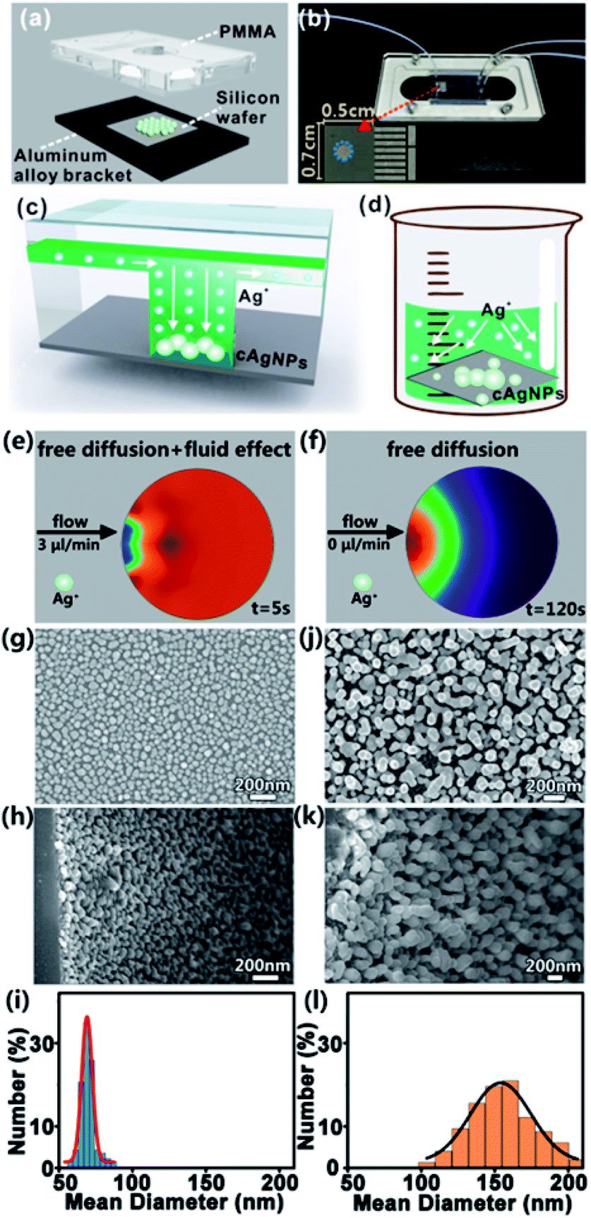 | ||
| Fig. 2 Characterization of cAgNPs. (a) Schematic diagram of the microfluidic device. (b) Photo of the microfluidic device. Schematic illustrations of silver ion (Ag+) diffusion and the formation of core AgNPs (cAgNPs) at the silicon surface in the (c) microfluidic or (d) bulk GD system. Simulations of silver ion diffusion in the microchamber with (e) or without microfluidic flow (f). (g) Top-view and (h) side-view SEM images of cAgNPs prepared in μ-GD systems and corresponding (i) histograms of size distribution. (j) Top-view and (k) side-view SEM images of cAgNPs prepared in bulk-GD systems and corresponding (l) histograms of size distribution. | ||
Of note, Ag+ transportation in the microfluidic system is the coupled process of creeping flowing and mass diffusion, while Ag+ transportation in the bulk system is only effected by mass diffusion. Accordingly, simulations of ion transportation in the microfluidic system (Fig. 2e) as well as in the bulk system (Fig. 2f) are systematically performed by using COMSOL multiphysics. Typically, homogeneous Ag+ distribution in the microfluidic system can be quickly reached within only 5 s, while Ag+ diffuses slowly and thus an apparent concentration gradient of Ag+ appears in the bulk system even when the simulating time is 120 s. The simulation results prove that the equilibrium of ion transportation can be rapidly achieved in the designed microfluidic system. The SEM images of cAgNPs prepared in the microchamber from the top view (Fig. 2g) and side view (Fig. 2h) confirm that the as-prepared cAgNPs with similar size and morphology are uniformly distributed on the silicon surface. In contrast, bulk GD synthesizes cAgNPs with broad size distribution, which are randomly dispersed on the silicon surface, as validated by the top-view SEM image (Fig. 2j) and side-view SEM image (Fig. 2k). For quantitative comparison, the size of the as-synthesized nanoparticles was determined by the measurement of 300 particles by using the software of Nano Measurer. As shown in the histograms of size distribution (Fig. 2i and l), the size distribution of cAgNPs prepared in the μ-GD system is much narrower than that in the bulk GD system under identical conditions. In particular, the diameter of cAgNPs prepared in the microfluidic system is ∼71 ± 18 nm, while the diameter of cAgNPs in the bulk system is ∼155 ± 57 nm.
To systematically investigate the effects of experimental conditions on the growth of cAgNPs, a series of SEM images of cAgNPs at different reaction time points, AgNO3 concentrations and AgNO3 flow rates are recorded. As shown in Fig. S1,† the size of cAgNPs prepared by microfluidics gradually increases with the reaction time, AgNO3 concentration and AgNO3 flow rate. However, if the reaction time is too long (e.g., > 4 min), the AgNO3 concentration is too high (e.g., > 0.75 mM) or the AgNO3 flow rate is too rapid (e.g., >3 μL min−1), the size distribution of cAgNPs becomes wide and the morphology of cAgNPs becomes irregular. As such, the optimal reaction conditions for synthesis of cAgNPs in the μ-GD system are 0.75 mM AgNO3, 4 min of reaction time and 3 μL min−1 flow rate.
SSE-encoded PANs by the μ-GD system
After the fabrication of homogeneous cAgNPs, 10 mM sodium phosphate buffer containing ∼300 nM SSEs (polyA–P1) is pumped into the input port with a relatively low flow rate (e.g., 0.5 μL min−1) for 8 h to ensure the efficient connection between polyA and cAgNPs. The preferential adsorption of the silver surface with polyA leads to the formation of the multi-valence engineered cAgNPs (Ag–polyA–P1). Then distilled water is pumped into the other input port, washing away the unconnected polyA–P1. Subsequently, 0.1 M sodium phosphate buffer containing ∼1 mM of AuNPs modified with polyA–P2 (Au–polyA–P2) is pumped into one input port with a relatively low flow rate of 0.5 μL min−1 for 12 h. During this process, the microfluidic device is placed on a heating plate at 37 °C. The appended recognition blocks of P1 and P2 favor DNA hybridization, resulting in the fabrication of SSE-encoded PANs. Ultimately, the formed high-valence PANs are rinsed with distilled water and dried with a flow of nitrogen for further characterization. As shown in the SEM image in Fig. 3a–c, several ∼10 nm AuNPs (Fig. S2†) are uniformly distributed on the surface of cAgNPs. The Au–Ag nanohybrids of PANs are also confirmed by UV-vis spectra (Fig. S3†). For clarity, AuNPs were intentionally colored using Adobe Photoshop.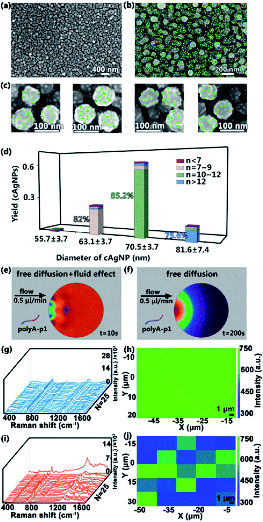 | ||
| Fig. 3 Characterization of SSE-encoded PANs. (a–c) SEM images of SSE-encoded PANs prepared in the microfluidic system at different magnifications. Scale bars are 400 nm, 200 nm and 100 nm. For clarity, the AuNPs in (b) and (c) are colored using Adobe Photoshop. (d) Statistical analysis of n-valence PANs (n < 7, n = 7–9, n = 10–12 and n > 12) corresponding to cAgNPs with different diameters. The total number of cAgNPs is 300. Simulations of SSE (polyA–P1) diffusion in the microchamber with (e) or without (f) microfluidic flow using COMSOL. (g) Raman spectra collected from the as-prepared PANs in the microfluidic system and corresponding SERS mapping results of the 730 cm−1 SERS peak (h). (i) Raman spectra collected from the as-prepared PANs in the bulk system and corresponding SERS mapping results of the 730 cm−1 SERS peak (j). | ||
The number of DNA molecules that can be functionalized on a NP surface depends fundamentally on the NP surface area. Thereby, the size of the core AgNPs as well as the size of satellite AuNPs used in the assembly of PANs will greatly affect the final “valences”. The number of AuNPs per cAgNPs(total number of cAgNPs is 300) is statistically analyzed in the histograms in Fig. 3d. Typically, among these 300 cAgNPs, ∼61% AgNPs have a diameter of 70.5 ± 3.7 nm and, of these, around 85.2% AgNPs have 11 ± 1 AuNPs bound to them; ∼25% AgNPs have a diameter of 63.1 ± 3.7 nm and, of these, around 82.0% AgNPs have 8 ± 1 AuNPs bound to them; ∼12% AgNPs have a diameter of 81.6 ± 7.4 nm and, of these, around 75.6% AgNPs have more than 12 AuNPs bound to them;2% AgNPs have a diameter of 55.7 ± 3.7 nm and, of these, around 55.2% AgNPs have less than 7 AuNPs bound to them. Indeed, the size of AgNPs is highly correlated with the number of covalent bonds. Analogously, the simulations of SSEs (polyA–P1) in the microfluidic system (Fig. 3e) and in the bulk system (Fig. 3f) are also performed using COMSOL multiphysics. Consequently, uniform SSE distribution in the microfluidic system can be quickly reached within 10 s, while the SSE concentration gradient is still obvious in the bulk system even when the simulating time is up to 200 s. The uniform SSE distribution leads to the uniform adsorption of SSEs on the surface of cAgNPs, which is also beneficial for the subsequent formation of the uniform PAN structure with similar valences after DNA hybridization.
To further clarify the distribution of DNA in the PAN structure, Raman characterization of the as-prepared nanostructures is performed. These nanostructures are made of DNA-engineered nanohybrids, and thus, in principle, there are lots of DNA sequences (i.e., polyA–P1, polyA–P2 and their hybridization products) in SERS hotspots.39,40 As revealed in Fig. 3g and i, the characteristic Raman peaks related to DNA molecules are clearly observed. Typically, the 730 cm−1 peak is assigned to the breathing and the ring skeleton vibration modes of adenine (A); the 787 cm−1 peak belongs to the ring breathing mode vibration of thymine (T) or cytosine (C); the 1475 cm−1 peak is mainly assigned to symmetric stretching vibration of the imidazole of guanine (G); the 1640 cm−1 peak is assigned to T and C (mainly T). The detailed assignments of Raman spectra are listed in Table S2.† The Raman spectra and SERS mapping in Fig. 3g–j originate from DNA molecules, serving as the linker in the PAN structure. As revealed in Fig. 3g and i, the characteristic Raman peaks related to DNA molecules are clearly observed (the detailed assignments of Raman spectra are listed in Table S2†). In addition, similar Raman spectra with nearly the same intensity are randomly collected from a square area in PAN synthesized by microfluidics (Fig. 3g and h), suggesting the uniform distribution of DNA in the ordered PAN structure. In contrast, the chaos of Raman spectra and SERS mapping is observed in bulk systems (Fig. 3i and j), suggesting that the distribution of DNA is not uniform in the unordered PAN structure in bulk systems. These Raman data demonstrate that microfluidics produces more uniform and ordered high-valence PANs over the ones made by bulk methods.
In order to understand the SERS effect of PANs, finite-difference time-domain (FDTD) simulations of the electromagnetic field (EM) intensity distribution in PANs, AgNPs@Si and AuNPs–AgNPs@Si (the AuNP solution is directly dripped onto the AgNPs surface) are performed, as shown in Fig. 4. The gap between AuNPs and AgNPs in PANs is set as 10 nm, and the gap between AuNPs and AgNPs in AuNPs-AgNPs@Si is set as 0 nm. Typically, the value of EM-field enhancement is ∼2.06 fold in AgNPs@Si, ∼6.98 fold in PANs and ∼18.84 fold in AuNPs–AgNPs@Si under the same testing conditions, indicating that relatively strong plasmonic coupling between AuNPs and AgNPs can be obtained by fabricating the PAN structure. However, due to no linker between Au and Ag nanoparticles, AuNPs are randomly distributed or even agglomerated on the AgNPs surface, and the RSD of the Rhodamine 6G (R6G) signal collected from AuNPs–AgNPs@Si is higher than 20%. The experimental results of Raman spectra are shown in Fig. S4,† which are consistent with the simulation results.
 | ||
| Fig. 4 FDTD simulation of the normalized EM-field intensity distribution (IEI2/IE0I2) for PAN, AgNP and Au–AgNP: (a) XZ and (b) XY plane view of a single PAN on the silicon substrate. (c) XZ and (d) XY plane view of a single AgNP on the silicon substrate. (e) XZ and (f) XY plane view of a single Au–AgNP (without DNA as a linker) on the silicon substrate. | ||
Next, the kinetics of SSE adsorption on cAgNPs are systematically investigated. Cy5-labeled SSEs (polyA–P1-Cy5) are pumped into the microchannel. The UV absorbance intensities of Cy5 in the initial SSEs and unconnected SSEs at each time point are recorded using a UV-vis spectrometer. Accordingly, the unconnected concentrations (C) of SSEs with different lengths (polyA15, polyA30 and polyA60) are calculated using the corresponding calibration curves in Fig. S5a.† Fig. S5b† shows the kinetic curves of polyA30–P1-Cy5 adsorption on cAgNPs in the bulk and microfluidic system. Typically, the value of C/C0 (C0, the initial concentration of SSEs) reaches its lowest point after reacting for 8 hours in the microfluidic system, or 12 hours in the bulk system, suggesting that polyA fully covers the surface of cAgNPs at this time. Moreover, the adsorption kinetics of polyA30–P1-Cy5 in the microfluidic system (e.g., Ka: 6.44 × 10⁻¹⁰ mol g−1 h−1) are much higher than those in the bulk system (e.g., Ka: 8.06 × 10⁻¹¹ mol g−1 h−1) (∼8-fold increase). As for the polyA with different lengths in the microfluidic system, the adsorption kinetics increase with the increase in length of polyA (Fig. S5c†) due to the increasing binding sites between SSEs and cAgNPs. Typically, Ka is 5.69 × 10⁻¹⁰ mol g−1 h−1 for polyA15, 6.44 × 10⁻¹⁰ mol g−1 h−1 for polyA30, and 8.84 × 10⁻¹⁰ mol g−1 h−1 for polyA60. Of note, the increased binding constant would not favor more strands of DNA associating with the surface. As such, the decrease in valence is attributed to a steric argument rather than kinetics.
Sample loading via microfluidics
Besides the high-yield fabrication of SSE-encoded PANs, the constructed microfluidic system can also be used for sample loading and on-line SERS detection. To primarily analyze the advantages of the developed microfluidic method in sample loading, 10−4 M R6G solution is pumped into the microchannel with a flow rate of 3 μL min−1. In comparison, R6G with the same concentration is dropped on the surface of SSE-encoded PANs directly, which is the most conventional sample loading method (Fig. 5a). We have obtained a real photo of a selected detection zone on the substrate and the corresponding SERS mapping of the Raman peak at 1364 cm−1 at the same location. As observed, when R6G solution is dropped onto the substrate via a pipette gun, there exists a ring-like zone in the photo image (Fig. 5b-I) due to the coffee ring effect. As further confirmed by the SERS mapping data, a ring-like SERS map is obtained from the same zone (Fig. 5b-II). Raman spectra from 30 random spots in a defined area of 10 × 10 μm2 are collected, and the RSD value of Raman intensities of R6G at 1364 cm−1 is ∼14.2% (Fig. 5c). In contrast, when the R6G solution is pumped onto the substrate via microfluidics, a “clean” chip could be observed in the photo image (Fig. 5e–I) due to R6G molecules being uniformly distributed on the substrate. Also, a uniform SERS map is attained from the same zone (Fig. 5e-II). And a lower RSD value of 5.6% can be achieved via on-line SERS detection (Fig. 5f), suggesting a better reproducibility of the developed sensing strategy. Besides for SSE-encoded PANs immobilized on a silicon wafer, the good reproducibility is also due to the fact that the control of fluids in the microfluidic channel leads to even distribution of analytes in the detection area of the substrate. | ||
| Fig. 5 Sample loading via microfluidics. (a) Schematic illustration of sample loading via a pipette gun. (b) Photo image (I) of the detection zone and the corresponding SERS mapping (II) of the Raman peak at 1364 cm−1 in the same location by the conventional sample loading method. (c) Corresponding Raman spectra of 10−4 M R6G directly dropped onto the prepared PANs. (d) Schematic illustration of sample loading via microfluidics. (e) Photo image (I) of the detection zone and corresponding SERS mapping (II) of the Raman peak at 1364 cm−1 in the same location by the microfluidic method. (f) Corresponding Raman spectra of 10−4 M R6G pumped onto the prepared PANs by microfluidics. | ||
PAN-based sensors for reliable quantitative TET analysis
The successful high-yield preparation of SSE-encoded PANs, sample loading and on-line SERS detection in the constructed microfluidic system prompt us to develop an automatic analytical platform, in which the fabrication of SSE-encoded PAN sensors, the injection of the sample and on-line measurement are all performed by the designed microfluidic chip. Moreover, in the SSE-encoded PAN sensors, SSEs are used not only as valence bonds to assemble PANs but also as internal standard (IS) molecules to correct the fluctuation of samples and measuring conditions. To our knowledge, there has been no report of this type of microfluidic analytical platform for reliable quantitative SERS analysis.Here, we attempt to use the microfluidic analytical platform for the detection of tetracycline (TET) spiked in 16 human serum samples and milk samples. TET as a typical broad spectrum antibiotic has been widely employed in veterinary medicine to combat bacteria. However, the accumulation of TET residues in the human body would result in serious health problems.41,42 As a result, TET has been listed as a pharmaceutical and personal care product (PPCPs) by the US environmental protection agency (EPA). In this regard, there is a great demand for the development of a sensitive, rapid and simple method for the detection of TET in real samples. However, it is still quite challenging to simultaneously realize ultrasensitive and reproducible determination of TET in real samples with the state-of-the-art SERS technology.
As schematically illustrated in Fig. 6a, the rigid dsDNA molecules made of Cyanine Dye 3 (Cy3) labeled TET aptamer and its corresponding cDNA are pumped into the microchannel and linked to SERS substrates of SSE-encoded PANs via thiol groups (please see the sequence details in ESI Table S1†). If there is no TET, dsDNA will sustain the rigid configuration, and thus the Raman reporter of Cy3 will be far away from the substrates, leading to weak Raman signals of Cy3 (signal off). In contrast, when TET exists in samples, cDNA will dissociate from dsDNA due to the formation of the flexible structure of the TET-aptamer complex. In this case, Cy3 is close to the SERS substrates, generating strong Raman signals of Cy3 (signal on). Of note, the TET sample solution in the microfluidic channel maintains a constant velocity when crossing the substrate, and thus the detection process is in a dynamic stable state. For testing different samples, the PAN-based SERS chip can be regenerated by replacing it with a clean silicon wafer, followed by assembly of PANs and functionalization of PANs under the same synthetic conditions. Owing to the precise control of the fluid by microfluidics with the injection pump and accurate optimization of synthesis parameters, the reaction conditions of each step including concentration, flowrate, temperature and reaction time can be well controlled. As a result, the PAN-based analytical platform is ready for reliable SERS detection.
 | ||
| Fig. 6 PAN-based automatic analytical platform for TET detection. (a) Schematic illustration of the PAN-based automatic analytical platform for TET detection. (b) Raman spectra of functionalized PANs, pure Raman dye of Cy3 and polyA30. (c) Raman spectra of functionalized PANs with different TET concentrations. (d) The linear fittings of the ratiometric signal (I1586/IBG, I1586/I730) versus the logarithmic concentration of TET. BG means background. (e) Raman spectra and (f) corresponding ratiometric signals (I1586/I730) from the functionalized PANs loaded in milk and serum samples (n = 16) spiked with different concentrations of TET. | ||
The Raman spectra of the constructed sensors are shown in Fig. 6b. Typically, the 730 cm−1 peak is assigned to the breathing and the ring skeleton vibration modes of polyA; the 1390 cm−1 peak, 1465 cm−1 peak, and 1586 cm−1 peak are assigned to the ν(C–N) stretching, ν(C![[double bond, length as m-dash]](https://www.rsc.org/images/entities/char_e001.gif) C) ring-stretching, and ν(CN) stretching modes of Cy3 (Table S3 †). Among these peaks, the Raman intensity of Cy3 at 1586 cm−1 is selected for quantitative comparison due to its prominent feature in the Cy3 spectrum. The signal change at 1586 cm−1 shows a TET concentration-dependent manner, which can be used to construct the corresponding calibration curve for quantification of an unknown content of TET (Fig. 6c). Of note, Raman peaks at 730 cm−1 of polyA don't overlap with the characteristic peaks of Cy3 at the excitation wavelength λex = 633 nm, and its intensity remains stable during the detection of TET due to polyA being tightly anchored on the plasmonic surfaces. As such, the signals of polyA at 730 cm−1 can serve as IS signals to normalize the variations of SERS signals. Without the calibration by IS signals of polyA, a poor linear relationship between the logarithmic concentration of TET and the corresponding SERS intensities of Cy3 at 1586 cm−1 is observed, with a low correlation coefficient (R2) of 0.920 (Fig. 6d). In contrast, a good linearity of the ratiometric signal (I1586/I730) versus the logarithmic concentration of TET exists with a high R2 of 0.999. Moreover, the constructed sensor displays an ultrahigh sensitivity with a limit of detection (LOD) of ∼4 fM, which is calculated by setting the signal-to-noise ratio to 3
C) ring-stretching, and ν(CN) stretching modes of Cy3 (Table S3 †). Among these peaks, the Raman intensity of Cy3 at 1586 cm−1 is selected for quantitative comparison due to its prominent feature in the Cy3 spectrum. The signal change at 1586 cm−1 shows a TET concentration-dependent manner, which can be used to construct the corresponding calibration curve for quantification of an unknown content of TET (Fig. 6c). Of note, Raman peaks at 730 cm−1 of polyA don't overlap with the characteristic peaks of Cy3 at the excitation wavelength λex = 633 nm, and its intensity remains stable during the detection of TET due to polyA being tightly anchored on the plasmonic surfaces. As such, the signals of polyA at 730 cm−1 can serve as IS signals to normalize the variations of SERS signals. Without the calibration by IS signals of polyA, a poor linear relationship between the logarithmic concentration of TET and the corresponding SERS intensities of Cy3 at 1586 cm−1 is observed, with a low correlation coefficient (R2) of 0.920 (Fig. 6d). In contrast, a good linearity of the ratiometric signal (I1586/I730) versus the logarithmic concentration of TET exists with a high R2 of 0.999. Moreover, the constructed sensor displays an ultrahigh sensitivity with a limit of detection (LOD) of ∼4 fM, which is calculated by setting the signal-to-noise ratio to 3![[thin space (1/6-em)]](https://www.rsc.org/images/entities/char_2009.gif) :1. The detailed calculation process of the LOD is provided in the ESI.† The obtained LOD is around four orders of magnitude lower than those of most reported TET sensors (see Table S4†). The developed TET sensor also exhibits good selectivity, as revealed in Fig. S6.† In real applications, serum and milk samples (n = 16) spiked with TET with different concentrations are measured using the developed sensors. As shown in Fig. 6e and f, the SERS spectra obtained from the TET standard solution and milk and human serum samples have no significant differences in both intensity and characteristic peaks. Furthermore, the recoveries of serum samples spiked with 1.12 nM, 11.2 nM, 112 nM and 1120 nM TET are 107%, 99%, 100% and 99%, and the corresponding RSD values are 4.0%, 3.9%, 3.8% and 1.3%, respectively. The recoveries of milk samples spiked with 1.12 nM, 11.2 nM, 112 nM, and 1120 nM TET are 107%, 100%, 101%, and 100% and the corresponding RSD values are 3.5%, 3.6%, 3.8% and 1.1%, respectively. In addition, the SERS experiments on SSE-encoded PANs synthesized in the bulk as a control were compared with the SERS experiments on SSE-encoded PANs synthesized in the microfluidic device. Specifically, as shown in Fig. S7,† owing to the uniform and ordered SSE-encoded PANs synthesized in the microfluidic device, they have a better reproducibility (RSD = 5.67%) in the detection of TET than SSE-encoded PANs synthesized in the bulk (RSD = 9.63%).
:1. The detailed calculation process of the LOD is provided in the ESI.† The obtained LOD is around four orders of magnitude lower than those of most reported TET sensors (see Table S4†). The developed TET sensor also exhibits good selectivity, as revealed in Fig. S6.† In real applications, serum and milk samples (n = 16) spiked with TET with different concentrations are measured using the developed sensors. As shown in Fig. 6e and f, the SERS spectra obtained from the TET standard solution and milk and human serum samples have no significant differences in both intensity and characteristic peaks. Furthermore, the recoveries of serum samples spiked with 1.12 nM, 11.2 nM, 112 nM and 1120 nM TET are 107%, 99%, 100% and 99%, and the corresponding RSD values are 4.0%, 3.9%, 3.8% and 1.3%, respectively. The recoveries of milk samples spiked with 1.12 nM, 11.2 nM, 112 nM, and 1120 nM TET are 107%, 100%, 101%, and 100% and the corresponding RSD values are 3.5%, 3.6%, 3.8% and 1.1%, respectively. In addition, the SERS experiments on SSE-encoded PANs synthesized in the bulk as a control were compared with the SERS experiments on SSE-encoded PANs synthesized in the microfluidic device. Specifically, as shown in Fig. S7,† owing to the uniform and ordered SSE-encoded PANs synthesized in the microfluidic device, they have a better reproducibility (RSD = 5.67%) in the detection of TET than SSE-encoded PANs synthesized in the bulk (RSD = 9.63%).
Conclusions
Herein, a novel synthetic strategy that combines μ-GD with polyA nanotechnology is developed for the achievement of homogeneous SSE-encoded PANs with high valences (n = 11 ± 1) and high yields (>80%) on a silicon wafer surface. In addition to the preparation of PANs conducted by the microfluidic chip, sample loading and on-line detection can also be achieved in the proposed microfluidic system. As such, an automatic PAN-based analytical platform is constructed, in which SSEs for the first time act as both linkers and IS molecules. By using the platform, as low as ∼4.0 fM TET can be readily determined, around four orders of magnitude lower than those by most reported sensors. In addition, the constructed platform is feasible for accurate determination of TET in serum and milk samples with a high recovery close to 100% and a low RSD less than 5.0%. The developed strategy offers a new paradigm in rapid and high-yield construction of complex PAN nanostructure-based platforms for biosensing and biological diagnostics.Experimental section
Fabrication of the home-made microfluidic system
The microfluidic device is composed of three layers: the upper polymethyl methacrylate (PMMA) chip, middle silicon wafer and bottom aluminum alloy bracket. The silicon wafer with a size of 0.7 cm × 0.5 cm is sandwiched between the microchamber and aluminum alloy bracket and fixed using a clamp.Fabrication of SSE-encoded PANs in the microfluidic system
To synthesize cAgNPs, hydrogen fluoride (HF) solution (5%, v/v) is pumped into the input port via a syringe pump (WH-SP-01, Wenhao Co., Ltd) first (3 μL min−1, 30 min). Next, HF solution (10%, v/v) containing 7.5 × 10⁻⁴ M silver nitrate (AgNO3) is pumped (3 μL min−1, 4 min). After the fabrication of cAgNPs, polyA–P1 (300 nM) in 10 mM phosphate buffer is pumped into the input port (0.5 μL min−1, 8 h) to ensure efficient connection between polyA and cAgNPs. And distilled water is pumped to wash away the unconnected polyA–P1. Subsequently, 0.1 M sodium phosphate buffer containing ∼1 mM AuNPs modified with polyA–P2 (Au–polyA–P2) is pumped into the input port to hybridize with polyA–P1 (37 °C, 12 h). The as-prepared PANs are rinsed with distilled water for the following studies.Fabrication of PAN-based TET sensors
For functionalization of PANs, double stranded DNA composed of a TET aptamer and its complementary DNA in phosphate buffer (pH = 7.0, 0.1 M NaCl, 100 nM dsDNA) is pumped into the input port (0.5 μL min−1, 12 h). Then, PBS buffer (pH 7.0) is pumped to wash away the unlinked DNA strands. Standard solutions, milk or serum samples containing TET with different concentrations are injected into one input port (2.5 μL min−1, 90 min). Then PBS buffer is injected into the other input port (2.5 μL min−1, 45 min) to remove dissociated cDNA strands. The Raman spectra of Cy3 are recorded by using a Raman microscope under 633 nm irradiation (100× objective, 1 s of acquisition time, 0.2 mW laser power). Each sample is used for three independent measurements.Conflicts of interest
There are no conflicts to declare.Acknowledgements
The authors state that all experiments were performed in strict accordance with the relevant laws and institutional guidelines. The Ethics Committee of the First Affiliated Hospital of Soochow University (Suzhou, China) approved the experiment. The authors also state that informed consent was obtained from all participants for any experiments with human serum samples without any identifying information. The First Affiliated Hospital of Soochow University is committed to the protection and safety of human serum samples involved in the research. All experimental procedures were completed under biosafety level II conditions. We thank Prof. Shuit-Tong Lee (Soochow University, China) and Dr Fei Peng (Harvard University, USA) for their general help and valuable suggestions. We appreciate the financial support from the National Natural Science Foundation of China (No. 21825402 and 22074101), the Natural Science Foundation of Jiangsu Province of China (No. BK20191417) and the Program for Jiangsu Specially-Appointed Professors to Prof. Yao He, a project funded by the Priority Academic Program Development of Jiangsu Higher Education Institutions (PAPD), the 111 Project and the Collaborative Innovation Center of Suzhou Nano Science and Technology (NANO-CIC).Notes and references
- C. A. Mirkin, R. L. Letsinger, R. C. Mucic and J. J. Storhoff, Nature, 1996, 382, 607–609 CrossRef CAS PubMed.
- R. J. Macfarlane, M. N. O. Brien, S. H. Petrosko and C. A. Mirkin, Angew. Chem., 2013, 52, 5688–5698 CrossRef CAS PubMed.
- M. R. Jones, N. C. Seeman and C. A. Mirkin, Science, 2015, 347, 1260901 CrossRef PubMed.
- S. Wang, J. S. Du, N. J. Diercks, W. Zhou, E. W. Roth, V. P. Dravid and C. A. Mirkin, J. Am. Chem. Soc., 2019, 141, 20443–20450 CrossRef CAS PubMed.
- C. Zhang, R. J. Macfarlane, K. L. Young, C. H. J. Choi, L. Hao, E. Auyeung, G. Liu, X. Zhou and C. A. Mirkin, Nat. Mater., 2013, 12, 741–746 CrossRef CAS PubMed.
- Y. Kim, R. J. Macfarlane, M. R. Jones and C. A. Mirkin, Science, 2016, 351, 579–582 CrossRef CAS PubMed.
- S. Y. Park, A. K. R. Lytton-Jean, B. Lee, S. Weigand, G. C. Schatz and C. A. Mirkin, Nature, 2008, 451, 553–556 CrossRef CAS PubMed.
- D. Samanta, A. Iscen, C. R. Laramy, S. B. Ebrahimi, K. E. Bujold, G. C. Schatz and C. A. Mirkin, J. Am. Chem. Soc., 2019, 141, 19973–19977 CrossRef CAS.
- J. Zhu, Y. Kim, H. Lin, S. Wang and C. A. Mirkin, J. Am. Chem. Soc., 2018, 140, 5061–5064 CrossRef CAS PubMed.
- Y. Xiang, Z. Wang, H. Xing and Y. Lu, Chem. Sci., 2013, 4, 398–404 RSC.
- L. Yang, L. Meng, J. Song, Y. Xiao, R. Wang, H. Kang and D. Han, Chem. Sci., 2019, 10, 7466–7471 RSC.
- X. Luo, C. Lachance-Brais, A. Bantle and H. F. Sleiman, Chem. Sci., 2020, 11, 4911–4921 RSC.
- Y. Zhang, S. Pal, B. Srinivasan, T. Vo, S. Kumar and O. Gang, Nat. Mater., 2015, 14, 840–848 CrossRef CAS PubMed.
- Y. Tian, T. Wang, W. Liu, H. L. Xin, H. Li, Y. Ke, W. M. Shih and O. Gang, Nat. Nanotechnol., 2015, 10, 637–644 CrossRef CAS PubMed.
- J. Shen, Q. Tang, L. Li, J. Li, X. Zuo, X. Qu, H. Pei, L. Wang and C. Fan, Angew. Chem., 2017, 56, 16077–16081 CrossRef CAS PubMed.
- L. Wang, M. Ren, L. Liang and C. Zhang, Chem. Sci., 2018, 9, 4942–4949 RSC.
- Y. Zhang, Y. Zhang, X. Zhang, Y. Li, Y. He, Y. Liu and H. Ju, Chem. Sci., 2020, 11, 6289–6296 RSC.
- M. Hu, C. Yuan, T. Tian, X. Wang, J. Sun, E. Xiong and X. Zhou, J. Am. Chem. Soc., 2020, 142, 7506–7513 CrossRef CAS PubMed.
- M. Wang, L. Dai, J. Duan, Z. Ding, P. Wang, Z. Li, H. Xing and Y. Tian, Angew. Chem., 2020, 132, 6451–6458 CrossRef.
- D. J. Lunn, J. R. Finnegan and I. Manners, Chem. Sci., 2015, 6, 3663–3673 ( Adv. Mater. , 2013 , 25 , 2779–2783 ) RSC.
- Y. Zhang, J. Chao, H. Liu, F. Wang, S. Su, B. Liu, L. Zhang, J. Shi, L. Wang, W. Huang, L. Wang and C. Fan, Angew. Chem., 2016, 128, 8168–8172 CrossRef.
- H. Xing, Y. Bai, Y. Bai, L. H. Tan, J. Tao, B. Pedretti, G. A. Vincil, Y. Lu and S. C. Zimmerman, J. Am. Chem. Soc., 2017, 139, 3623–3626 CrossRef CAS.
- Y. Wang, Y. Wang, D. R. Breed, V. N. Manoharan, L. Feng, A. D. Hollingsworth, M. Weck and D. J. Pine, Nature, 2012, 491, 51–56 CrossRef CAS PubMed.
- T. G. W. Edwardson, K. L. Lau, D. Bousmail, C. J. Serpell and H. F. Sleiman, Nat. Chem., 2016, 8, 162–170 CrossRef CAS PubMed.
- G. Yao, J. Li, Q. Li, X. Chen, X. Liu, F. Wang, Z. Qu, Z. Ge, R. P. Narayanan, D. Williams, H. Pei, X. Zuo, L. Wang, H. Yan, B. L. Feringa and C. Fan, Nat. Mater., 2020, 19, 781–788 CrossRef CAS PubMed.
- B. Zhao, J. Shen, S. Chen, D. Wang, F. Li, S. Mathur, S. Song and C. Fan, Chem. Sci., 2014, 5, 4460–4466 RSC.
- H. Pei, F. Li, Y. Wan, M. Wei, H. Liu, Y. Su, N. Chen, Q. Huang and C. Fan, J. Am. Chem. Soc., 2012, 134, 11876–11879 CrossRef CAS PubMed.
- D. Zhu, P. Song, J. Shen, S. Su, J. Chao, A. Aldalbahi, Z. Zhou, S. Song, C. Fan, X. Zuo, Y. Tian, L. Wang and H. Pei, Anal. Chem., 2016, 88, 4949–4954 CrossRef CAS PubMed.
- D. Zanchet, C. M. Micheel, W. J. Parak, D. Gerion and A. P. Alivisatos, Nano Lett., 2001, 1, 32–35 CrossRef CAS.
- K. S. Elvira, X. C. i Solvas, R. C. R. Wootton and A. J. deMello, Nat. Chem., 2013, 5, 905–915 CrossRef CAS PubMed.
- D. Zhang, F. Wu, M. Peng, X. Wang, D. Xia and G. Guo, J. Am. Chem. Soc., 2015, 137, 6263–6269 CrossRef CAS PubMed.
- L. Zhang, Y. Wang, L. M. Tong and Y. N. Xia, Nano Lett., 2014, 14, 4189–4194 CrossRef CAS PubMed.
- M. Q. Lu, S. K. Yang, Y. P. Ho, C. L. Grigsby, K. W. Leong and T. J. Huang, ACS Nano, 2014, 8, 10026–10034 CrossRef CAS PubMed.
- L. Zhang, G. Niu, N. Lu, J. Wang, L. Tong, L. Wang, M. J. Kim and Y. N. Xia, Nano Lett., 2014, 14, 6626–6631 CrossRef CAS PubMed.
- S. E. Lohse, J. R. Eller, S. T. Sivapalan, M. R. Plews and C. J. Murphy, ACS Nano, 2013, 7, 4135–4150 CrossRef CAS PubMed.
- Y. Liu and X. Jiang, Lab Chip, 2017, 17, 3960–3978 RSC.
- H. Wang, Y. Zhou, X. Jiang, B. Sun, Y. Zhu, H. Wang, Y. Su and Y. He, Angew. Chem., Int. Ed., 2015, 54, 5132–5136 CrossRef CAS PubMed.
- Y. M. A. Yamada, Y. Yuyama, T. Sato, S. Fujikawa and Y. Uozumi, Angew. Chem., Int. Ed., 2014, 126, 131–135 CrossRef.
- L. J. Xu, Z. C. Lei, J. Li, C. Zong, C. J. Yang and B. Ren, J. Am. Chem. Soc., 2015, 137, 5149–5154 CrossRef CAS PubMed.
- A. I. Pérez-Jiménez, D. Lyu, Z. Lu, G. Liu and B. Ren, Chem. Sci., 2020, 11, 4563–4577 RSC.
- M. A. Fischbach and C. T. Walsh, Science, 2009, 325, 1089–1093 CrossRef CAS.
- L. Ge, H. Li, X. Du, M. Zhu, W. Chen, T. Shi, N. Hao, Q. Liu and K. Wang, Biosens. Bioelectron., 2018, 111, 131–137 CrossRef CAS PubMed.
Footnotes |
| † Electronic supplementary information (ESI) available. See DOI: 10.1039/d0sc05911k |
| ‡ These authors contributed equally to this work. |
| This journal is © The Royal Society of Chemistry 2021 |