
 Open Access Article
 This Open Access Article is licensed under a Creative Commons Attribution-Non Commercial 3.0 Unported Licence
Room temperature conductance switching in a molecular iron(III) spin crossover junction†
Senthil Kumar
Karuppannan
 a,
Alejandro
Martín-Rodríguez
b,
Eliseo
Ruiz
*b,
Phimphaka
Harding
*c,
David J.
Harding
*c,
Xiaojiang
Yu
d,
Anton
Tadich
e,
Bruce
Cowie
f,
Dongchen
Qi
f and
Christian A.
Nijhuis
*ag
a,
Alejandro
Martín-Rodríguez
b,
Eliseo
Ruiz
*b,
Phimphaka
Harding
*c,
David J.
Harding
*c,
Xiaojiang
Yu
d,
Anton
Tadich
e,
Bruce
Cowie
f,
Dongchen
Qi
f and
Christian A.
Nijhuis
*ag
aDepartment of Chemistry, National University of Singapore, 3 Science Drive, Singapore 117543, Singapore. E-mail: chmnca@nus.edu.sg
bDepartament de Química Inorgànica, Institut de Recerca de Química Teòrica i Computacional, Universitat de Barcelona, Diagonal 645, 08028 Barcelona, Spain. E-mail: eliseo.ruiz@qi.ub.edu
cFunctional Materials and Nanotechnology Center of Excellence, Walailak University, Thasala, Nakhon Si Thammarat 80160, Thailand. E-mail: kphimpha@mail.wu.ac.th; hdavid@mail.wu.ac.th
dSingapore Synchrotron Light Source, National University of Singapore, 5 Research Link, Singapore 117603, Singapore
eAustralian Synchrotron Clayton, Victoria 3168, Australia
fSchool of Chemistry and Physics, Queensland University of Technology, Brisbane, Queensland 4001, Australia
gCentre for Advanced 2D Materials & Graphene Research, National University of Singapore, 6 Science Drive 2, Singapore 117546, Singapore
First published on 10th November 2020
Abstract
Herein, we report the first room temperature switchable Fe(III) molecular spin crossover (SCO) tunnel junction. The junction is constructed from [FeIII(qsal-I)2]NTf2 (qsal-I = 4-iodo-2-[(8-quinolylimino)methyl]phenolate) molecules self-assembled on graphene surfaces with conductance switching of one order of magnitude associated with the high and low spin states of the SCO complex. Normalized conductance analysis of the current–voltage characteristics as a function of temperature reveals that charge transport across the SCO molecule is dominated by coherent tunnelling. Temperature-dependent X-ray absorption spectroscopy and density functional theory confirm the SCO complex retains its SCO functionality on the surface implying that van der Waals molecule—electrode interfaces provide a good trade-off between junction stability while retaining SCO switching capability. These results provide new insights and may aid in the design of other types of molecular devices based on SCO compounds.
Introduction
Spin crossover (SCO) molecules are promising candidates in the development of various spintronic and data storage devices as they can switch between two electronic states, defined by their high spin (HS) and low spin (LS) states.1–3 Given that switching can be triggered by various external stimuli, such as, temperature, pressure, light, or adsorption of guest molecules, SCO molecules also find applications as smart materials that respond to several stimuli. Devices based on thin films4–7 (with a thickness of typically 10–100 nm) of SCO molecules exhibit spin-polarized current switching,8 voltage-bias,9 and stretching10 induced resistance switching, and memristive properties,11 but it is still challenging, however, to incorporate SCO molecules in molecular tunnel junctions as they are prone to decomposition, or conformational distortion, such that they lose their SCO properties.4,5,8 In addition, the molecule–electrode coupling has to be optimized because too strong molecule–electrode coupling leads to drastic alteration of their magnetic properties, even a complete loss of SCO behaviour,12–14 yet too weak coupling compromises stability of the devices.11,15 A summary of these different parameters for the SCO molecule-based junctions is given in Table S1.† Here we report a molecular tunnel junction with a monolayer (unlike the more common multi-layers) of FeIII SCO molecules adsorbed via self-assembly on single-layer graphene on Cu and with EGaIn top-contacts that can be switched between HS and LS states at a remarkably high-temperature T = 310 K resulting in a 10-fold change in the conductivity of the junction. Importantly, both electrodes form van der Waals contacts with the SCO molecules ensuring an optimal trade-off between junction stability and coupling strength so that the SCO properties are retained in contrast to other approaches that rely on covalent or electrostatic interactions and in which the interface chemistry is often not controlled. Spectroscopy and DFT calculations show that, unlike other systems, the FeIII state is preserved illustrating the potential of FeIII SCO materials as a new class of switchable molecular materials.As noted above overly strong molecule—electrode coupling interactions can result in the adsorption of mixtures of HS and LS molecules. Consequently, the relative population of the two spin states cannot be changed by external stimuli.11,13,15 For example, thin films of [Fe(NCS)2(phen)2] on Cu(100) traps the molecules in either the HS or LS state, but adding a CuN layer decouples the SCO molecules from the substrate allowing them to be electrically switched.15 To reduce the electrode—molecule coupling strength, highly oriented pyrolytic graphite (HOPG) has been used as a substrate onto which SCOs form non-covalent monolayers.16–19 This strategy resulted in thermally and light-activated SCO monolayers17,18 likely because the van der Waals interactions between SCO molecules and HOPG are weaker than between SCO molecules and bare metals.
While the above thin films show promise, molecular SCO devices are still rare. Using break junctions, [Fe(bpp-py)2]2+ (bpp-py = 2,6-(bis(pyrazol-1-yl)-4-pyridyl)pyridine)20 and [Fe(tpy-R)(tpy-R′)]2+ (tpy-R = substituted terpyridine)21 showed voltage-induced switching of the spin sate. Van der Zant and co-workers showed that [Fe(tpy-C6H4-S)2] placed between two gold electrodes can be stretched to induce a change in the spin state and conductance.21 An inherent challenge with break junctions is the high failure rate and difficulty in achieving consistent orientation of the molecules in the junction. Recently, [Fe(HB(tz)3)2] molecules have been incorporated in large-area junctions1–4,22 in the form of thin films (6–100 nm thick), but depending on the fabrication methods either conductance switching was associated with a LS → HS transition,7 or HS → LS4,5 highlighting the challenges in controlling the characteristics of the device.
Despite these successes, comparatively few systems have been used in molecular junctions, almost all of them are FeII SCOs, and in many cases, the switching occurs only at very low temperatures.11,23–25 By comparison, despite their greater robustness, FeIII SCO complexes are almost entirely absent in SCO molecular junctions. The first report involved subliming [Fe(pap)2]ClO4 (pap = N-2-pyridylmethylidene-2-hydroxyphenylaminato) onto Au(111), but only a small proportion of the molecules were switchable.11 Use of Cu2N islands on the Au(111) surface decouples the SCO molecules from the Au and allowed for more efficient electrical switching using an STM tip at low T = 4.5 K.24 Nevertheless, the harshness of the deposition technique risks changing the oxidation state of the iron centre and it was not confirmed that the SCO molecules remain in the FeIII state on the surface.
To address these challenges to obtain robust molecular SCO junctions, we selected [FeIII(qsal-I)2]NTf2 (qsal-I = 4-iodo-2-[(8-quinolylimino)methyl]phenolate) as it exhibits a strongly hysteretic spin transition at room temperature.26 We have shown before that single-layer graphene (SLG) on Cu (Cu//SLG where “//” denotes a van der Waals interface) is an excellent platform to form stable monolayers of functional molecules due to favorable van der Waals interactions27 yet without charge transfer between the molecules and the surface ensuring the molecular frontier orbitals remain localized on the molecules;28 we have used this approach to make efficient molecular diodes. Here we report that Cu//SLG//[FeIII(qsal-I)2]NTf2//GaOx/EGaIn junctions (the EGaIn top-electrode also forms a van der Waals contact with the monolayer, Fig. 1) show clear spin-state switching, leading to one order of magnitude change in conductance. These results are supported by extensive theoretical modeling and represent the first example of a room temperature switchable FeIII SCO molecular junction.
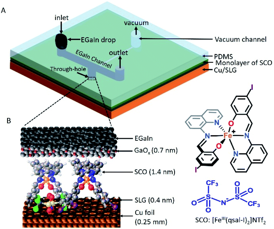 | ||
| Fig. 1 (A) Schematic illustration of the SCO molecule based device with the EGaIn top-electrode stabilized in a small through-hole in a rubber stamp (made of PDMS) and (B) the SCO based molecular junction of the form of Cu//SLG//[FeIII(qsal-I)2]NTf2//GaOx/EGaIn (EGaIn = eutectic alloy of Ga and In). | ||
Results and discussion
Characterization of the Cu//SLG//[FeIII(qsal-I)2]NTf2
The device architecture is illustrated in Fig. 1. Briefly, graphene was grown on Cu foil using the chemical vapour deposition method, as described elsewhere.29 The synthesis of [FeIII(qsal-I)2]NTf2 has been reported elsewhere.26 We physisorbed [FeIII(qsal-I)2]NTf2 onto the SLG by immersing the CU//SLG substrate in a 1.0 mM solution of [FeIII(qsal-I)2]NTf2 in CH2Cl2. We formed junctions by contacting a monolayer of physisorbed [FeIII(qsal-I)2]NTf2 with GaOx/EGaIn to-electrodes (EGaIn stands for eutectic gallium–indium; 75.5% Ga and 24.5% In by weight). Here, the EGaIn was stabilized in a through-hole in polydimethylsiloxane (PDMS) and the fabrication of this top contact has been reported elsewhere.30We used Raman spectroscopy to determine the quality of the graphene31 and to obtain additional information regarding the graphene–molecule interactions. The important features in the Raman spectra of graphene are the sharp peak at ∼1587 cm−1 which corresponds to the first order Raman scattering process in graphene (called the G band) and the second order peak involving two phonons at 2678 cm−1 is associated with two phonons (called a 2D band). In the case of disordered graphene, we can also observe another second order peak at about half of the frequency of the 2D band (∼1200 cm−1), which is called the disorder-induced D-band involving one phonon and one defect. The relative intensity of the D-band is directly proportional to the level of defects in the sample.31Fig. 2A shows the Raman spectrum of our pristine Cu//SLG sample. The intensity ratio of 2D and G band (I2D/IG) is 2.52 for our graphene samples confirming our samples consist of SLG (additional graphene layers causes a decrease of the I2D/IG ratio, even to <1). In addition, the full width at half maximum (FWHM) of the 2D band peak of our sample is 27 cm−1 which is close to that of ∼30 cm−1 commonly reported for SLG (the FWHM increase up to ∼60 cm−1 for multi-layer graphene). After adsorption of [FeIII(qsal-I)2]NTf2, the 2D peak blue shifts by 19 cm−1 which corresponds to a Fermi level shift of the graphene of +0.45 eV (estimated as described in ref. 32). This blue shift indicates that the molecules interact, besides van der Waals interactions, with moderate electrostatic interactions with the Cu//SLG surface. The I2D/IG after adsorption decreases to 1.20 confirming adsorption of the [FeIII(qsal-I)2]NTf2 molecule on SLG. The lack of a D peak indicates that upon adsorption of [FeIII(qsal-I)2]NTf2 the sp2 bond character of graphene is preserved and that the number of defects is insignificant.
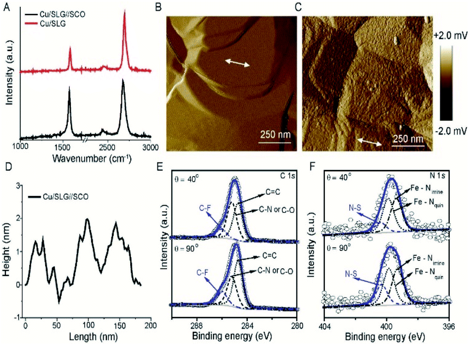 | ||
| Fig. 2 (A) Raman spectra of SLG before (red) and after adsorption (black) of [FeIII(qsal-I)2]NTf2. AFM amplitude images of (B) bare graphene and (C) after adsorption of [FeIII(qsal-I)2]NTf2 and the corresponding AFM height profiles (D). Angle dependent X-ray photoelectron spectra of (E) C 1s, and (F) N 1s (see section S1 for all other spectra). | ||
Fig. 2B shows the atomic force microscopy (AFM) image of the bare Cu//SLG from which we conclude that the surface is homogeneous. Fig. 2C shows the AFM image after functionalization with a monolayer of SCO which shows the monolayer is homogeneous as no pinhole or nano/microcrystallites are visible. The height of the islands of SCO molecules which are between 1.5–2.0 nm, consistent with the height of the [Fe(qsal-I)2]NTf2 molecule of 1.41 nm (Fig. 2D). Based on these results we conclude that [Fe(qsal-I)2]NTf2 is present as a homogeneous monolayer on Cu//SLG.
To confirm the chemical composition and relative orientation of [FeIII(qsal-I)2]NTf2 on the Cu//SLG surface, we characterized the surfaces with angle-resolved XPS (ARXPS; Fig. 2E and F; section S2). The C 1s spectra are characterized by 3 peaks assigned to the CF3 group, present in the counter anion of [FeIII(qsal-I)2]NTf2, at 286.0 eV, and two peaks at 285.2 eV and 284.6 eV corresponding to C![[double bond, length as m-dash]](https://www.rsc.org/images/entities/char_e001.gif) N and C–O groups, and CC groups, respectively, present in the ligands of [FeIII(qsal-I)2]NTf2. The quantitative analysis of the spectra is consistent with the chemical formula of [FeIII(qsal-I)2]NTf2 (Table S2†). The relative peak intensity of the CF3 signal increases when the emission angle (θ) increases from 40° to 90° which suggests that the anions are adsorbed on the graphene surface. Similar observations are observed in the F 1s spectra, but more importantly also in the I 3d spectra which indicates that the iodines interact with the graphene surface. This orientation of [FeIII(qsal-I)2]NTf2 is further supported by the N 1s (Fig. 2F) spectra, where the peak at 400.3 eV for the N–S group also depends on θ, whereas the peaks at 399.3 and 399.9 eV corresponding to Fe–Nimine and Fe–Nquin are independent of θ. Collectively, the ARXPS data strongly suggest that the counteranions are adsorbed on the graphene resulting in a Cu//SLG//[FeIII(qsal-I)2]+NTf2 configuration driven by van der Waals interactions between the (highly polarizable) iodines and the graphene. This is consistent with the observed blue shift (electron doping due to the electron-donating nature of the counteranions) in the Raman spectra (Fig. 2A) upon the adsorption of [FeIII(qsal-I)2]NTf2 onto the graphene surface.
N and C–O groups, and CC groups, respectively, present in the ligands of [FeIII(qsal-I)2]NTf2. The quantitative analysis of the spectra is consistent with the chemical formula of [FeIII(qsal-I)2]NTf2 (Table S2†). The relative peak intensity of the CF3 signal increases when the emission angle (θ) increases from 40° to 90° which suggests that the anions are adsorbed on the graphene surface. Similar observations are observed in the F 1s spectra, but more importantly also in the I 3d spectra which indicates that the iodines interact with the graphene surface. This orientation of [FeIII(qsal-I)2]NTf2 is further supported by the N 1s (Fig. 2F) spectra, where the peak at 400.3 eV for the N–S group also depends on θ, whereas the peaks at 399.3 and 399.9 eV corresponding to Fe–Nimine and Fe–Nquin are independent of θ. Collectively, the ARXPS data strongly suggest that the counteranions are adsorbed on the graphene resulting in a Cu//SLG//[FeIII(qsal-I)2]+NTf2 configuration driven by van der Waals interactions between the (highly polarizable) iodines and the graphene. This is consistent with the observed blue shift (electron doping due to the electron-donating nature of the counteranions) in the Raman spectra (Fig. 2A) upon the adsorption of [FeIII(qsal-I)2]NTf2 onto the graphene surface.
Temperature-dependent XAS and XMCD
To confirm the spin transition in the SCO molecule on the graphene surface, we performed X-ray absorption spectroscopy (XAS) as a function of the temperature of the Cu//SLG//[FeIII(qsal-I)2]NTf2 monolayer. The Fe L2,3 edge shows different edge shapes33 as well as a distinct chemical shift between divalent and trivalent states,34 which allows qualitative statements about the valence state of the metal complex. The obtained separation of Fe L3 and Fe L2 maxima from the XAS spectra (Fig. S2†), due to spin–orbit coupling of 13.9 eV, is in good agreement with previously reported data for the trivalent state of iron.5,34Fig. 3A shows the results of the XAS spectra for Fe L3 edge of the 2p3/2 core hole recorded at T = 260, 300, and 340 K along with simulations using CTM4XAS software.33,35,36 The spectra are dominated by one peak at 709.3 eV associated with a FeIII complex (red solid line), and a small shoulder is visible at 707.9 eV corresponding to the FeII complex (blue solid line). Based on the relative areas underneath the peaks, we conclude that 98% of the Fe-ions on the surface are present in the form of the FeIII complex. The L3 edge spectra shift to higher photon energies by ∼0.6 eV with decreasing T. Upon spin crossover from the LS to the HS state, the Fe–L bond length increases causing the coordination sphere to expand, thereby reducing the ligand-field splitting of the Fe 3d orbitals by ∼0.6 eV, which is consistent with the estimated energy difference of 13.8 kcal mol−1 (0.59 eV) for HS to LS by the DFT model discussed below. | ||
| Fig. 3 (A) The X-ray absorption spectra (XAS) of the Fe L3 edge for a monolayer of [FeIII(qsal-I)2]NTf2 on graphene at different temperatures, along with simulated peaks for octahedral (Oh) Fe2+ and Fe3+ ions obtained with the CTM4XAS program. The XAS spectra of Fe L3 edges for two different external magnetic field directions at (B) 340 K, (C) 300 K, and (D) 260 K. The difference between the XAS signals observed at +1.5 T and −1.5 T defines the XMCD signal. | ||
The branching ratio (b), defined as37,38
| b = I3/(I3 + I2) | (1) |
We performed temperature-dependent XAS measurements of our SCO compound in powder form to confirm whether the switching characteristics of the SCO molecule on graphene are similar to that of the powder form. Fig. S3† shows the Fe L2,3 edge spectra with spin–orbit coupling energy of 13.4 eV which confirms the presence of FeIII in the SCO complex. Both L2 (720 eV) and L3 (707 eV) edges shift to higher binding energy with decreasing temperature from 340 K to 120 K, which confirms the HS to LS transition of the molecule occurs at lower temperature in the powder form (see Fig. S3B† for T dependent magnetic hysteresis loop) as compared to that of the molecule on the graphene surface in agreement with a previously reported transition of the SCO molecule in powder form where the transition temperature T1/2 for cooling is 248 K and T1/2 for heating is 278 K.26,39
To further confirm the spin transition of the monolayers on graphene, we recorded the X-ray magnetic circular dichroism (XMCD) spectra in total electron yield mode with a magnetic field applied to the sample, which is parallel to the circularly polarized photoelectron propagation vector. All the spectra are reported with a magnetic field of ±1.5 T at different temperatures. Fig. 3B–D show the results for the Fe L3 edge and that the HS complex shows a higher XMCD signal than the LS complex.40 The observed negative XMCD signal (Fig. 3B) at a photon energy of 710.3 eV indicates the presence of spin-polarized FeIII with octahedral symmetry.36,41Fig. 3D shows only a weak negative XMCD signal at 710 eV at 260 K which indicates that the SCO complex switches from HS (S = 5/2) to LS (S = 1/2) (see DFT calculations below) since the LS state has a smaller number of uncompensated spins than the HS state. It is important to note that, we only have a monolayer of the SCO complex adsorbed on the surface, and consequently, the signal is very small which prevents us to quantitatively fit to the spectra.15 These results are consistent with the magnetic susceptibility measurement of the SCO molecule in powder form reported before showing an abrupt SCO transition with noticeable hysteresis.26 Thus, the observed results lead to the utilization of the spin-state conductance switching on the graphene surface for the independent switchability of the magnetic molecules in magnetic tunnel junctions at room temperature.
Charge transport measurements
To investigate how the tunnelling characteristics of the junctions change with T, we determined the electrical properties with a statistically large number of J(V) curves to allow us to select devices which had their characteristics within one log-standard deviation for temperature dependent measurements using well-established methods.42–44 We fabricated 50 Cu//SLG//[FeIII(qsal-I)2]NTf2//GaOx/EGaIn junctions with cone-shaped tips of EGaIn using 8 different substrates with a yield of non-shoring junctions of 88%. Fig. 4A shows the heatmap of all J(V) curves (1150 in total) along with the Gaussian log-average current densities, 〈log10|J|〉G, (solid black line). The log-standard deviations, σlog,G, fall in the range of 0.4 to 0.8 which are comparable to other highly reproducible EGaIn junctions.29,30,45–48 Given the high yields and small spread in the data we conclude the formation of Cu//SLG//[FeIII(qsal-I)2]NTf2//EGaIn junctions is highly reproducible. None of the junctions shorted during 25 consecutive J(V) sweeps from which we conclude that the junctions are stable.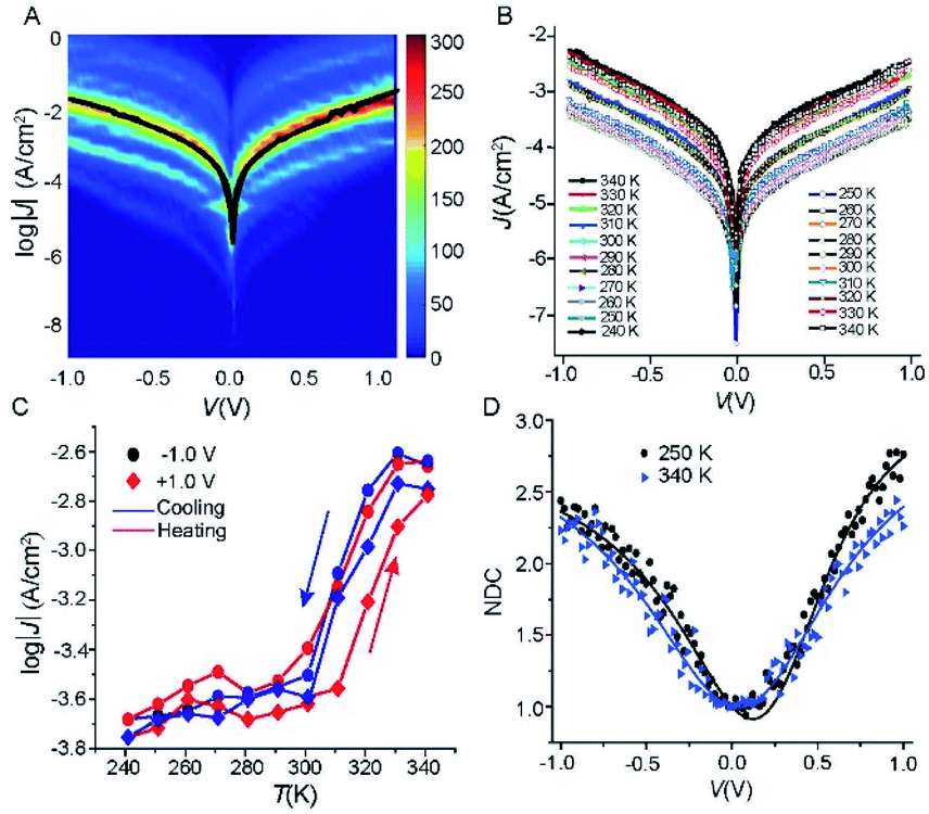 | ||
| Fig. 4 (A) Heatmap of log│J│ vs. (V) curves, the solid black line is the 〈log10|J|〉Gvs. V curve. (B) J(V) curves recorded as a function of temperature 340 → 240 → 340 K at intervals of 10 K for Cu//SLG//[FeIII(qsal-I)2]NTf2//GaOx/EGaIn junction. (C) J as a function of temperature at ±1.0 V applied bias (solid lines are visual guides), and (D) normalized differential conductance for the Cu//SLG//[FeIII(qsal-I)2]NTf2//GaOx/EGaIn junction at different temperature; solid lines are fits to the eqn (2). | ||
We measured the J(V) curves of Cu//SLG//[FeIII(qsal-I)2]NTf2//GaOx/EGaIn junctions as a function of temperature (T = 240–340 K) using EGaIn stabilized in a through-hole in a microfluidic network in PDMS (polydimethylsiloxane) following a previously reported method30 (section S3). Fig. 4B shows the J(V) characteristics recorded while cooling and subsequent heating of the junction (Fig. S4 and S5† show another 2 sets of data). Fig. 4C shows the corresponding evolution of the values of J at −1.0 and +1.0 V. The observed difference in the width and the position of the hysteresis under positive and negative bias polarity is most likely due to small conformational differences of the SCO complex similar to observations made by Miyamachi et al.15 and Poggini et al.4 Moreover, from these data we make the following 3 observations. (1) The value of J changes by one order of magnitude with T. This large switch in the observed current proves that FeIII complexes can perform similarly well as FeII complexes and the transition from HS → LS does not preclude efficient current switching in molecular junctions. In the case of Fe(II) complexes the two spin states HS and LS are paramagnetic and diamagnetic, respectively. It has been suggested that as both spin states are paramagnetic in the case of Fe(III), the magnitude of the change in current upon SCO would be less for Fe(III) compared to Fe(II).5,15 Our results show that this is not necessarily true. (2) The SCO transition occurs around room temperature from 300 to 330 K. This switching temperature is consistent with the XAS and XMCD results discussed above. (3) The SCO transition of [FeIII(qsal-I)2]NTf2 in the junction is more gradual with the average transition temperature T1/2 (the temperature at which 50% HS to LS conversion) shifted from 263 (for [FeIII(qsal-I)2]NTf2 in the powder form) to ca. 300 K. As our original report showed,26 and more recent work confirms, the hysteresis in [FeIII(qsal-I)2]NTf2 is intimately associated with a conformational change in the NTf2 anion.49 The adsorption of the NTf2 anions on the SLG surface likely prevents such conformational change and the presence of only a single layer of [FeIII(qsal-I)2]+ cations will further reduce cooperativity leading to an increase in the spin transition temperature and a loss of hysteresis in the junction.49 It is noteworthy that in the [Fe(HB(trz)3)2] system, which also incorporates an EGaIn top-electrode, a small shift in T1/2 to higher temperature is observed.5 Moreover, a very recent report with an Fe(III) compound shows a shift from 80 K (bulk) to 200 K (junction).50 These results show that the Cu//SLG is a promising platform to anchor SCO molecules in a stable manner without compromising their SCO behaviour.
Recently, the SCO behaviour of Au//[FeII(HB(trz)3)2]//Ga2O3/EGaIn junctions with 6.7 nm thick films (∼7 molecular layers) directly adsorbed on Au was reported. Here, an anomalous SCO transition was observed within 1 K for which no explanation was given.5 In a follow up study, a very broad SCO transition from 100–300 K was reported for Au//[Fe(H2B(pz)2)2(phen)]//GaOx/EGaIn junctions with 5.6 nm thick molecular films. The authors proposed a switch in the mechanism of charge transport from coherent tunnelling in the LS state to incoherent tunnelling (or hopping) in the HS state. However, a plateau of the current state at high T was not observed and Arrhenius plots of the low or high conductance states were not reported, hampering elucidation of the mechanism of charge transport experimentally.4
In general, to establish the mechanism of charge transport it is important to perform J(V) measurements as a function of T.5,48,51,52 Coherent tunnelling is independent of the T, and the J(V) curve is parabolic in nature.51,52 In contrast, incoherent tunnelling (or hopping) is thermally activated where charges hop to available molecule energy states causing deviations from parabolic behaviour,53 and strongly depends on the T and weakly dependents on the tunneling distance. However, to elucidate the mechanism of charge transport across the Cu//SLG//[FeIII(qsal-I)2]NTf2//GaOx/EGaIn junctions in the high and low conduction states, we performed normalized differential conductance (NDC) analysis using eqn (2), as described before,51,52 to determine whether the J(V) curves are parabolic.
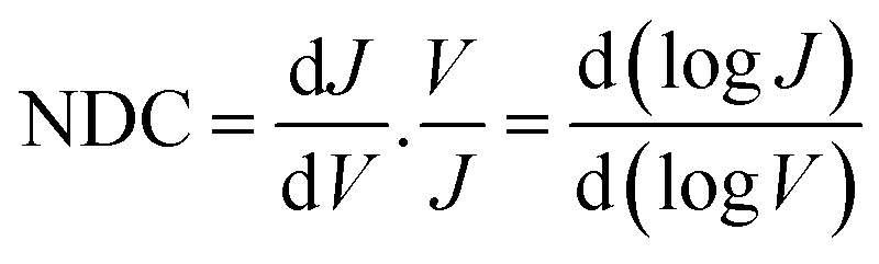 | (2) |
For the NDC analysis we used the individual J(V) traces obtained at 340 and 250 K. Fig. 4D shows the NDC curves show typical parabolic behaviour approaching NDC = 3 at ±1.0 V characteristic for coherent tunnelling. The NDC plots show a small asymmetry which is likely due to the different top and bottom electrode materials. The calculations below show that molecular orbitals are available (i.e., have their energies close to the energy of the Fermi level, EF) for charge transport which explains the relatively high tunnelling currents (10–100 times higher than for junctions with conjugated molecules of similar length that are dominated by off resonant tunnelling54–56). Therefore, we conclude that the dominant mechanism of charge transport is resonant coherent tunnelling.
Theoretical modelling of the junction
We modelled the complex structure of the EGaIn electrode by starting with the X-ray structure of α-gallium57 [100] onto which a monolayer of O2 molecules was placed. We added randomly positioned Ga and In atoms following the experimental stoichiometric ratio of EGaIn (the eutectic is composed of 75.5% Ga and 24.5 Ga% In by weight) to obtain the fully optimized top electrode. Different binding conformations of [FeIII(qsal-I)2]NTf2 with SLG were considered (see section S2), but the conformation with the two iodine atoms interacting with graphene is the most stable one (see Fig. 5), which is consistent with the XPS result discussed earlier. We hypothesize that a combination of anion⋯π and I⋯π interactions aid non-covalent attachment of [FeIII(qsal-I)2]NTf2 to the graphene surface. Finally, the complete junction including the Cu//SLG bottom electrode was fully optimized for the high- and low-spin states of the metal complex (the cif files of the optimized structures can be found in the ESI, Fig. S6†).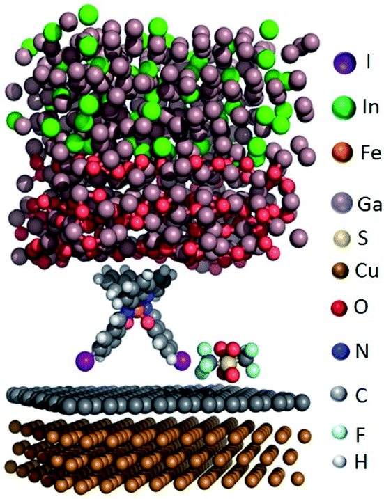 | ||
| Fig. 5 Representation of the optimized unit cell for the high-spin system. | ||
The relative stability of the two states of the metal complex was computed using the non-hybrid meta-GGA SCAN functional, which indicates that the S = 1/2 low-spin state is the ground state, which is 28.0 kcal mol−1 (1.21 eV) more stable than the S = 5/2 high-spin state, which is consistent with the observed shift (1.66 eV) in the XAS spectra of the powder form of [FeIII(qsal-I)2]NTf2 (Fig. S3†).26 Here we report that the stabilization of the HS state can be compensated due to a change in the entropy of a few kcal mol−1 depending on the transition temperature, i.e., the experimental T1/2 is 263 K.26 We used the hybrid meta-GGA TPSSh function to calculate the HS-LS energy difference in the [FeIII(qsal-I)2]NTf2 molecule on the monolayer. The HS-LS energy difference (computed meta-GGA TPSSh functional) is 13.8 kcal mol−1 (0.59 eV), which is consistent with the observed energy shift of 0.6 eV for HS-LS conversion in the temperature-dependent XAS spectra (Fig. 3A).
The calculation of the transport properties was performed using Siesta/Gollum codes.58,59 In the zero-voltage limit, we can approximate the conductance (G) as described in eqn (3) in G0 units.
| GV>0 = T(EF)G0 | (3) |
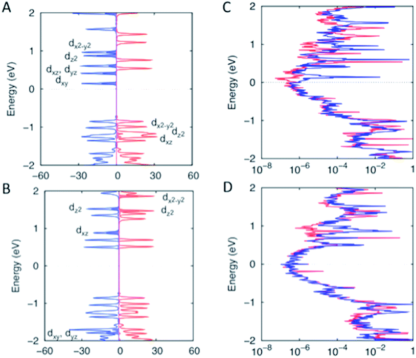 | ||
| Fig. 6 Projected density of states (PDOS) of [Fe(qsal-I)2]NTf2 for the high spin state (A) and low spin state (B). The projected transmission spectrum of [Fe(qsal-I)2]NTf2 for the high spin state (C) and low spin state (D). Red and blue colors stand for alpha and beta spin–orbitals. The filled curves are the PDOS of the FeIII metal. | ||
Conclusions
In summary, we have demonstrated the first successful use of a FeIII SCO molecule in a molecular junction for fully reversible room temperature conductance switching. The junction is easy to fabricate, involving physisorption of the SCO molecule onto a graphene surface, highly reproducible, and stable. The ARXPS measurements indicate that the counteranion is adsorbed on the graphene with the [Fe(qsal-I)2]+ cation on top. This arrangement effectively decouples the SCO molecule from the Cu electrode allowing reversible SCO to be observed in the molecular junctions, as evidenced by XAS and XMCD studies. The J(V) data are analysed with NDC analysis which confirms that charge transport is dominated by tunnelling for HS and LS. The experimental studies are supported by detailed theoretical calculations, which also highlight the critical importance of the EGaIn top electrode in stabilizing the Fe-centre in the 3+ oxidation state by forming van der Waals contacts between the molecule and the electrode. These results represent a new frontier in FeIII SCO materials, and given the relative simplicity of our approach will, we believe, be applicable to a wide range of switchable molecular materials, leading to new discoveries in molecular electronics.Conflicts of interest
There are no conflicts to declare.Acknowledgements
We gratefully acknowledge the support of the Thailand Research Fund (BRG6180008) in funding this research. P.H. thanks the Office of National Higher Education Science Research and Innovation Policy Council for additional funding (PMUB-B05F630101). This work had Financial Support by the Ministerio de Ciencia e Innovación through grant PGC2018-093863-B-C21 and MDM-2017-0767 and Generalitat de Catalunya with the grant SGR2017-1289. E.R. thanks Generalitat de Catalunya for his ICREA Academia grant. A.M.R. thanks Ministerio de Ciencia e Innovación for a predoctoral FPI fellowship. We thank the BSC for computational resources, technical expertise, and assistance. We express thanks to the Ministry of Education singapore for supporting this research (award no. MOE2018-T2-1-088), and the Prime Minister's Office, Singapore, under its Medium-Sized Centre program. We kindly acknowledge the Singapore Synchrotron Light Source (SSLS) supporting our experiments at the SINS beamline under NUS core support C-380-003-003-001. We would like to acknowledge Soft X-ray (SXR) Beamline at the Australian Synchrotron.References
- K. Senthil Kumar and M. Ruben, Coord. Chem. Rev., 2017, 346, 176–205 CrossRef CAS.
- C. Lefter, V. Davesne, L. Salmon, G. Molnár, P. Demont, A. Rotaru and A. Bousseksou, Magnetochemistry, 2016, 2, 18 CrossRef.
- A. Bousseksou, G. Molnár, L. Salmon and W. Nicolazzi, Chem. Soc. Rev., 2011, 40, 3313–3335 RSC.
- L. Poggini, M. Gonidec, R. K. C. Balasubramanyam, L. Squillantini, G. Pecastaings, A. Caneschi and P. Rosa, J. Mater. Chem. C, 2019, 7, 5343–5347 RSC.
- L. Poggini, M. Gonidec, J. H. González-Estefan, G. Pecastaings, B. Gobaut and P. Rosa, Adv. Electron. Mater., 2018, 4, 1800204 CrossRef.
- C. Lefter, S. Rat, J. S. Costa, M. D. Manrique-Juárez, C. M. Quintero, L. Salmon, I. Séguy, T. Leichle, L. Nicu, P. Demont, A. Rotaru, G. Molnár and A. Bousseksou, Adv. Mater., 2016, 28, 7508–7514 CrossRef CAS.
- V. Shalabaeva, K. Ridier, S. Rat, M. D. Manrique-Juarez, L. Salmon, I. Séguy, A. Rotaru, G. Molnár and A. Bousseksou, Appl. Phys. Lett., 2018, 112, 013301 CrossRef.
- A. C. Aragonès, D. Aravena, J. I. Cerdá, Z. Acís-Castillo, H. Li, J. A. Real, F. Sanz, J. Hihath, E. Ruiz and I. Díez-Pérez, Nano Lett., 2016, 16, 218–226 CrossRef.
- H. Hao, T. Jia, X. Zheng, L. Song and Z. Zeng, J. Mater. Chem. C, 2017, 5, 11598–11604 RSC.
- R. Frisenda, G. D. Harzmann, J. A. Celis Gil, J. M. Thijssen, M. Mayor and H. S. J. Van Der Zant, Nano Lett., 2016, 16, 4733–4737 CrossRef CAS.
- T. Jasper-Toennies, M. Gruber, S. Karan, H. Jacob, F. Tuczek and R. Berndt, Nano Lett., 2017, 17, 6613–6619 CrossRef CAS.
- M. Mannini, P. Sainctavit, R. Sessoli, C. Cartier dit Moulin, F. Pineider, M.-A. Arrio, A. Cornia and D. Gatteschi, Chem.–Eur. J., 2008, 14, 7530–7535 CrossRef CAS.
- A. Pronschinske, Y. Chen, G. F. Lewis, D. A. Shultz, A. Calzolari, M. Buongiorno Nardelli and D. B. Dougherty, Nano Lett., 2013, 13, 1429–1434 CrossRef CAS.
- S. Beniwal, X. Zhang, S. Mu, A. Naim, P. Rosa, G. Chastanet, J.-F. Létard, J. Liu, G. E. Sterbinsky, D. A. Arena, P. A. Dowben and A. Enders, J. Phys.: Condens. Matter, 2016, 28, 206002 CrossRef CAS.
- T. Miyamachi, M. Gruber, V. Davesne, M. Bowen, S. Boukari, L. Joly, F. Scheurer, G. Rogez, T. K. Yamada, P. Ohresser, E. Beaurepaire and W. Wulfhekel, Nat. Commun., 2012, 3, 936–938 CrossRef.
- M. S. Alam, M. Stocker, K. Gieb, P. Müller, M. Haryono, K. Student and A. Grohmann, Angew. Chem., Int. Ed., 2010, 49, 1159–1163 CrossRef CAS.
- L. Kipgen, M. Bernien, S. Ossinger, F. Nickel, A. J. Britton, L. M. Arruda, H. Naggert, C. Luo, C. Lotze, H. Ryll, F. Radu, E. Schierle, E. Weschke, F. Tuczek and W. Kuch, Nat. Commun., 2018, 9, 2984 CrossRef.
- M. Bernien, H. Naggert, L. M. Arruda, L. Kipgen, F. Nickel, J. Miguel, C. F. Hermanns, A. Krüger, D. Krüger, E. Schierle, E. Weschke, F. Tuczek and W. Kuch, ACS Nano, 2015, 9, 8960–8966 CrossRef CAS.
- M. Bernien, D. Wiedemann, C. F. Hermanns, A. Kruüger, D. Rolf, W. Kroener, P. Muüller, A. Grohmann and W. Kuch, J. Phys. Chem. Lett., 2012, 3, 3431–3434 CrossRef CAS.
- V. Meded, A. Bagrets, K. Fink, R. Chandrasekar, M. Ruben, F. Evers, A. Bernand-Mantel, J. S. Seldenthuis, A. Beukman and H. S. J. Van Der Zant, Phys. Rev. B, 2011, 83, 1–13 CrossRef.
- G. D. Harzmann, R. Frisenda, H. S. J. Van Der Zant and M. Mayor, Angew. Chem., Int. Ed., 2015, 54, 13425–13430 CrossRef CAS.
- Y. Zhang, I. Séguy, K. Ridier, V. Shalabaeva, M. Piedrahita-Bello, A. Rotaru, L. Salmon, G. Molnár and A. Bousseksou, J. Phys.: Condens. Matter, 2020, 32, 214010 CrossRef CAS.
- T. G. Gopakumar, M. Bernien, H. Naggert, F. Matino, C. F. Hermanns, A. Bannwarth, S. Mühlenberend, A. Krüger, D. Krüger, F. Nickel, W. Walter, R. Berndt, W. Kuch and F. Tuczek, Chem.–Eur. J., 2013, 19, 15702–15709 CrossRef CAS.
- T. Jasper-Tönnies, M. Gruber, S. Karan, H. Jacob, F. Tuczek and R. Berndt, J. Phys. Chem. Lett., 2017, 8, 1569–1573 CrossRef.
- G. Serrano, E. Velez-Fort, I. Cimatti, B. Cortigiani, L. Malavolti, D. Betto, A. Ouerghi, N. B. Brookes, M. Mannini and R. Sessoli, Nanoscale, 2018, 10, 2715–2720 RSC.
- N. Phukkaphan, D. L. Cruickshank, K. S. Murray, W. Phonsri, P. Harding and D. J. Harding, Chem. Commun., 2017, 53, 9801–9804 RSC.
- B. Long, M. Manning, M. Burke, B. N. Szafranek, G. Visimberga, D. Thompson, J. C. Greer, I. M. Povey, J. MacHale, G. Lejosne, D. Neumaier and A. J. Quinn, Adv. Funct. Mater., 2012, 22, 717–725 CrossRef CAS.
- P. Song, S. Guerin, S. J. R. Tan, H. V. Annadata, X. Yu, M. Scully, Y. M. Han, M. Roemer, K. P. Loh, D. Thompson and C. A. Nijhuis, Adv. Mater., 2018, 30, 1706322 CrossRef.
- P. Song, C. S. S. Sangeeth, D. Thompson, W. Du, K. P. Loh and C. A. Nijhuis, Adv. Mater., 2016, 28, 631–639 CrossRef CAS.
- A. Wan, L. Jiang, C. S. S. Sangeeth and C. A. Nijhuis, Adv. Funct. Mater., 2014, 24, 4442–4456 CrossRef CAS.
- L. M. Malard, M. A. Pimenta, G. Dresselhaus and M. S. Dresselhaus, Phys. Rep., 2009, 473, 51–87 CrossRef CAS.
- C. F. Chen, C. H. Park, B. W. Boudouris, J. Horng, B. Geng, C. Girit, A. Zettl, M. F. Crommie, R. A. Segalman, S. G. Louie and F. Wang, Nature, 2011, 471, 617–620 CrossRef CAS.
- A. Bhattacharyya, E. Stavitski, J. Dvorak and C. E. Martínez, Geochim. Cosmochim. Acta, 2013, 122, 89–100 CrossRef CAS.
- P. A. Van Aken and B. Liebscher, Phys. Chem. Miner., 2002, 29, 188–200 CrossRef CAS.
- E. Stavitski and F. M. F. de Groot, Micron, 2010, 41, 687–694 CrossRef CAS.
- M. Sassi, C. I. Pearce, P. S. Bagus, E. Arenholz and K. M. Rosso, J. Phys. Chem. A, 2017, 121, 7613–7618 CrossRef CAS.
- K. S. Kumar, M. Studniarek, B. Heinrich, J. Arabski, G. Schmerber, M. Bowen, S. Boukari, E. Beaurepaire, J. Dreiser and M. Ruben, Adv. Mater., 2018, 30, 1–7 Search PubMed.
- B. Warner, J. C. Oberg, T. G. Gill, F. El Hallak, C. F. Hirjibehedin, M. Serri, S. Heutz, M. A. Arrio, P. Sainctavit, M. Mannini, G. Poneti, R. Sessoli and P. Rosa, J. Phys. Chem. Lett., 2013, 4, 1546–1552 CrossRef CAS.
- W. Thammasangwan, P. Harding, S. G. Telfer, A. Alkaş, W. Phonsri, K. S. Murray, R. Clérac, M. Rouzières, G. Chastanet and D. J. Harding, Eur. J. Inorg. Chem., 2020, 1325–1330 CrossRef CAS.
- J. K. Kowalska, B. Nayyar, J. A. Rees, C. E. Schiewer, S. C. Lee, J. A. Kovacs, F. Meyer, T. Weyhermüller, E. Otero and S. DeBeer, Inorg. Chem., 2017, 56, 8147–8158 CrossRef CAS.
- E. Lee, D. H. Kim, J. Hwang, K. Lee, S. Yoon, B. J. Suh, K. Hyun Kim, J.-Y. Kim, Z. H. Jang, B. Kim, B. I. Min and J.-S. Kang, Appl. Phys. Lett., 2013, 102, 133703 CrossRef.
- W. F. Reus, C. A. Nijhuis, J. R. Barber, M. M. Thuo, S. Tricard and G. M. Whitesides, J. Phys. Chem. C, 2012, 116, 6714–6733 CrossRef CAS.
- C. A. Nijhuis, W. F. Reus, J. R. Barber and G. M. Whitesides, J. Phys. Chem. C, 2012, 116, 14139–14150 CrossRef CAS.
- C. S. S. Sangeeth, A. Wan and C. A. Nijhuis, J. Am. Chem. Soc., 2014, 136, 11134–11144 CrossRef CAS.
- A. Krzykawska, M. Wróbel, K. Kozieł and P. Cyganik, ACS Nano, 2020, 14, 6043–6057 CrossRef CAS.
- O. E. Castañeda Ocampo, P. Gordiichuk, S. Catarci, D. A. Gautier, A. Herrmann and R. C. Chiechi, J. Am. Chem. Soc., 2015, 137, 8419–8427 CrossRef.
- H. J. Um, G. D. Kong and H. J. Yoon, ACS Appl. Mater. Interfaces, 2018, 10, 34758–34764 CrossRef CAS.
- K. S. Kumar, R. R. Pasula, S. Lim and C. A. Nijhuis, Adv. Mater., 2016, 28, 1824–1830 CrossRef CAS.
- J. J. Whittaker, P. Harding, J. K. Clegg and D. J. Harding, Cryst. Growth Des., 2020, 20, 7006–7011 CrossRef CAS.
- A. Gee, A. H. Jaafar, B. Brachňaková, J. Massey, C. H. Marrows, I. Šalitroš and N. T. Kemp, J. Phys. Chem. C, 2020, 124, 13393–13399 CrossRef CAS.
- A. Vilan, J. Phys. Chem. C, 2007, 111, 4431–4444 CrossRef CAS.
- S. K. Karuppannan, E. H. L. Neoh, A. Vilan and C. A. Nijhuis, J. Am. Chem. Soc., 2020, 142, 3513–3524 CrossRef CAS.
- A. Vercik, L. C. O. Vercik and G. Bueno, J. Appl. Phys., 2019, 125, 025101 CrossRef.
- T. Wang, W. Du, N. Tomczak, L. Wang and C. A. Nijhuis, Adv. Sci., 2019, 6, 1970122 CrossRef.
- Y. Zhang, X. Qiu, P. Gordiichuk, S. Soni, T. L. Krijger, A. Herrmann and R. C. Chiechi, J. Phys. Chem. C, 2017, 121, 14920–14928 CrossRef CAS.
- Y. Zhang, S. Soni, T. L. Krijger, P. Gordiichuk, X. Qiu, G. Ye, H. T. Jonkman, A. Herrmann, K. Zojer, E. Zojer and R. C. Chiechi, J. Am. Chem. Soc., 2018, 140, 15048–15055 CrossRef CAS.
- A. Rühm, H. Reichert, W. Donner, H. Dosch, C. Grütter and J. Bilgram, Phys. Rev. B: Condens. Matter Mater. Phys., 2003, 68, 1–11 CrossRef.
- J. M. Soler, E. Artacho, J. D. Gale, A. García, J. Junquera, P. Ordejón and D. Sánchez-Portal, J. Phys.: Condens. Matter, 2002, 14, 2745–2779 CrossRef CAS.
- J. Ferrer, C. J. Lambert, V. M. García-Suárez, D. Z. Manrique, D. Visontai, L. Oroszlany, R. Rodríguez-Ferradás, I. Grace, S. W. D. Bailey, K. Gillemot, H. Sadeghi and L. A. Algharagholy, New J. Phys., 2014, 16, 093029 CrossRef.
- M. Di Ventra, Electrical Transport in Nanoscale Systems, Cambridge University Press, Cambridge, 2008, p. 126 Search PubMed.
Footnote |
| † Electronic supplementary information (ESI) available: The XPS characterization (section S1, and Fig. S1), device characteristics of various SCO junction (Table S1), the temperature dependent XAS spectra of powder SCO sample, and detailed theoretical analysis (section S2). See DOI: 10.1039/d0sc04555a |
| This journal is © The Royal Society of Chemistry 2021 |