
 Open Access Article
 This Open Access Article is licensed under a Creative Commons Attribution-Non Commercial 3.0 Unported Licence
Enhanced open-circuit voltages and efficiencies: the role of oxidation state of molybdenum oxide buffer layer in polymer solar cells†
Pengfei Maa,
Jiaying Xu *a,
Chen Wangc,
Changhao Wanga,
Fanxu Meng*b,
Yupeng Xiea and
Shanpeng Wenc
*a,
Chen Wangc,
Changhao Wanga,
Fanxu Meng*b,
Yupeng Xiea and
Shanpeng Wenc
aCollege of Science, Jilin Institute of Chemical Technology, Jilin 132022, P. R. China. E-mail: xujiaying@jlict.edu.cn
bCenter of Analysis and Measurement, Jilin Institute of Chemical Technology, Jilin 132022, P. R. China. E-mail: mfxoped2019@126.com
cState Key Laboratory on Integrated Optoelectronics and College of Electronic Science & Engineering, Jilin University, Changchun 130012, P. R. China
First published on 29th October 2021
Abstract
Molybdenum oxide (MoOx) is widely used as a buffer layer in optoelectronic devices to improve the charge extraction efficiency. The oxidation state of MoOx plays an important role in determining its electrical properties. However, there are few studies on the oxidation state to further guide the optimization of the MoOx buffer layer. In this work, inverted-structured polymer solar cells (PSCs) with a MoOx buffer layer were fabricated. Post-air annealing was used to control the cation valence state in MoOx. X-ray photoelectron spectroscopy (XPS), ultraviolet photoelectron spectroscopy (UPS), atomic force microscopy (AFM) and transient photocurrent (TPC) were employed to study the valence state, energy level, morphology of the MoOx layers and the photovoltaic property and charge transfer efficiency of the devices. It was found that the oxidation state was effectively improved by the post-annealing process. As a result, the work function of MoOx was raised and the hole mobility was improved. The open-circuit voltages and the efficiencies of PTB7-Th:PC71BM based PSCs were enhanced from 0.77 V and 8.66% to 0.81 V and 10.01%, respectively. The results show that high oxidation state MoOx provides optimized energy level alignment, reduced defects and better charge transfer efficiency, which is more in line with the requirement of buffer layer materials for optoelectronic applications.
Introduction
Organic photovoltaics is considered as a promising technology for harvesting energy from solar radiation owing to the potential advantages of stability, low cost, light weight, flexibility and large-scale fabrication.1–5 Recently, polymer solar cells (PSCs) have been significantly developed with power conversion efficiencies (PCEs) over 18%.6–8 These encouraging results not only rely on the design and synthesis of new materials and the microstructure optimization of the active layer,9–13 but this is also inseparable from the exploration of device fabrication technologies and electrode interface engineering.14–16 The application of inverted structures has made significant contribution to improve the performance and stability of PSCs, owing to the advantages of vertical phase separation of the active layer and reduction of reaction with water and oxygen.17–19The development of electrode buffer materials and interface modification engineering also plays an important role in the improvement of PCE.20–23 High work function (WF) transition-metal oxides such as molybdenum oxide (MoOx), vanadium oxide, and tungsten oxide are generally used as hole transport layer (HTL) to improve charge extraction efficiency in inverted structure devices.24–27 Among them, MoOx have demonstrated promising potential of non-toxic nature, easy evaporation, high carrier mobility and suitable energy levels.28–31 However, the evaporated MoOx film generally contains oxygen vacancies. These oxygen vacancies provide additional electrons like n-type doping and change the MoOx to lower oxidation state.32–34 As a result, the Fermi level of MoOx shifts toward the conduction band and the WF was decreased, which may decrease the built-in electric field at polymer/MoOx interface and thus lower the open-circuit voltage (VOC) of PSCs. Moreover, the oxygen vacancies may also act as traps for interfacial carrier recombination, resulting in energy losses. Considering the decreased WF of MoOx can also directly affects the level alignment between MoOx and organic active layer heterojunction, the efficiency of charge transfer at polymer/MoOx interface, which is relied on suitable level alignment, will further influenced by the oxidation state.
In this work, we attempt to reduce the performance degradation of PSCs caused by low oxidation state in MoOx layer by air annealing. During the inverted PSCs fabrication process, MoOx films were deposited by thermal evaporation followed by thermal annealing in air atmosphere. It was found that all the parameters of PSCs were improved especially for the VOCs. We further investigated the oxidation state, morphology, energy level structure of the MoOx layers and charge transfer in the devices. This study will provide optimized technological parameters for the fabrication of MoOx layer and theoretical basis for applications in optoelectronic devices.
Results and discussion
Fig. 1 illustrate the post-air annealing treatment, the device structure and the chemical structures of active layer materials. PSCs with inverted structure of ITO/ZnO/PTB7-Th:PC71BM/MoOx/Al were fabricated. Firstly, to investigate the effect of air annealing on photovoltaic performance, the devices were annealed in air after MoOx layer deposited. Fig. 2 shows the current density–voltage (J–V) curves and PCEs of as-prepared and post-annealed devices. It can be found that the VOCs were markedly improved form 0.77 V to 0.81 V and the FFs were also improved from 62.12% to 67.35% by post-annealing treatment. The photovoltaic parameters are listed in Table 1. As a result, a champion PCE of 10.01% was achieved by post-annealed devices, compared with 8.66% of as-prepared devices. These results reveal that post-annealing treatment can effectively improve the performance of PSCs.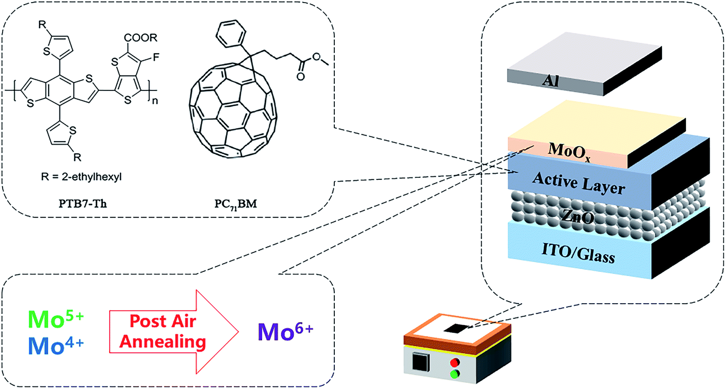 | ||
| Fig. 1 Illustration of the chemical structures of active layer materials, the device structure and the post-air annealing treatment. | ||
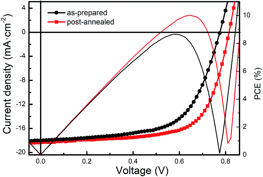 | ||
| Fig. 2 J–V curves and PCEs of the as-prepared and post air-annealed PSCs based on PTB7-Th. | ||
| VOC (V) | JSC (mA cm−2) | FF (%) | PCE (%) | ||
|---|---|---|---|---|---|
| Max. | Aver. | ||||
| As-prepared devices | 0.77 ± 0.01 | 17.68 ± 0.33 | 61.33 ± 0.89 | 8.66 | 8.38 |
| Post-air annealed devices | 0.81 ± 0.01 | 18.20 ± 0.24 | 66.78 ± 0.57 | 10.01 | 9.84 |
| Annealed in glovebox | 0.77 ± 0.01 | 18.11 ± 0.29 | 62.17 ± 0.41 | 8.84 | 8.68 |
| Only active layer annealed | 0.77 ± 0.01 | 17.70 ± 0.12 | 56.11 ± 0.51 | 7.79 | 7.68 |
Then we cast the post-annealing treatment in glovebox as control to verify the role of air in the above process. Fig. 3 shows the J–V curves. Unlike air annealing, post-annealing in glovebox did not make difference to the VOCs. Only the JSCs and FFs were slightly larger than the as-prepared devices, which improve the PCEs less than 0.2%. Hence it can be concluded that the air is the key factor in the post-annealing.
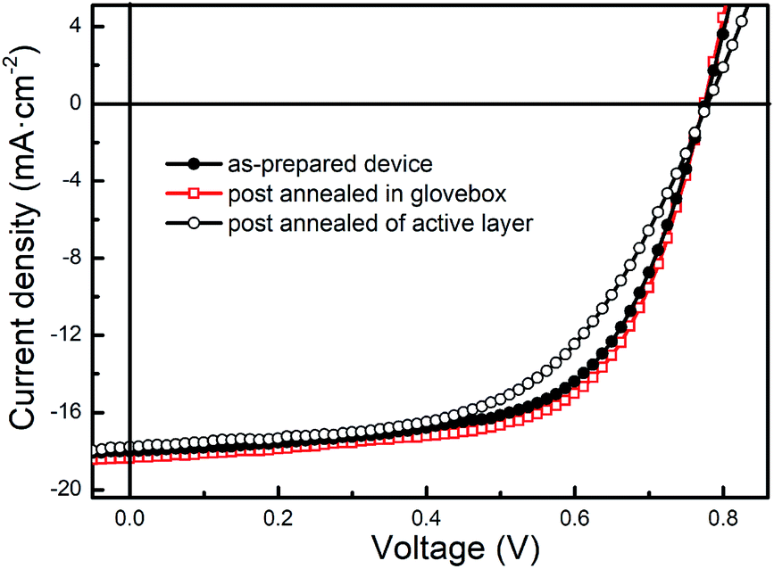 | ||
| Fig. 3 J–V curves of the PTB7-Th-based PSCs which were as-prepared, post-annealed in glovebox and only active layer annealed. | ||
To ensure the improvement was resulted from post-annealing of MoOx layer, only active layer annealed devices, which were annealed in air before MoOx layer deposited, were fabricated as control. As Fig. 3 shows, the VOC and JSC of active layer annealed devices were very closed to the as-prepared devices, but the FF was reduced signally. Hence the PCE was also reduced to 7.79%. Therefore, it was MoOx layer which improved by air annealing treatment, and thus contributed to PSCs performance.
The above findings encouraged us to find out how the air annealing affect the MoOx layer. X-ray photoelectron spectroscopy (XPS) was used to investigate the chemical compositions and cation oxidation state of MoOx films. The experimental and fitted XPS spectra of Mo 3d state for as-deposited and post-annealed MoOx films were shown in Fig. 4. The Mo 3d peak of post-annealed MoOx shifted to higher binding energy compared to the as-deposited one, which indicate the proportion of Mo6+ in MoOx films was increased after air annealing. According to reported literature, oxygen vacancies can be created during the evaporation in vacuum, so reduced oxidation states (Mo4+ and Mo5+) are created by electrons trapped in such oxygen vacancies.32 By air-annealing treatment, the vacancies were filled with oxygen atoms, the electrons were transferred from Mo atoms, and thus the oxidation states of MoOx was enhanced. The reduced oxygen vacancies will restrain the carrier recombination in interface and promote the hole extraction of MoOx.
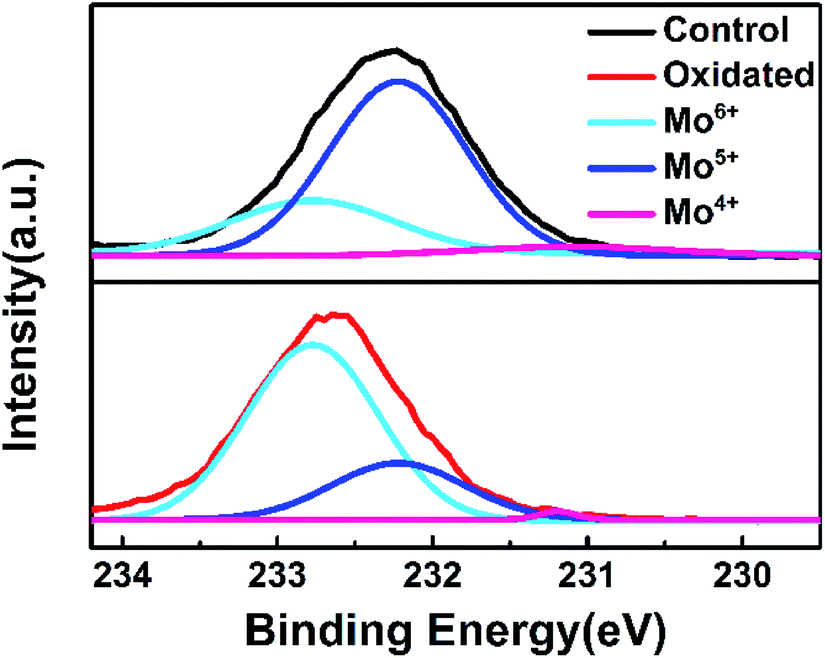 | ||
| Fig. 4 The XPS spectra of Mo 3d state for as-deposited and post-annealed MoOx films. | ||
The larger proportion of Mo6+ may raise the WF. Then we performed ultraviolet photoelectron spectroscopy (UPS) measurements to verify the energy levels of the MoOx. As Fig. 5(a) shows, the WF of MoOx was raised from 5.12 eV to 5.45 eV after air-annealing. This can be explained by the fact that the oxygen vacancies in MoOx make neighbored Mo6+ gain electrons which can move freely within the film, like n-type doping cases. Combined with the XPS results, it can be inferred that air-annealing transfers Mo5+ or Mo4+ back to Mo6+ and restrains excess electron generation, and thus raise the WF.33 Fig. 5(b) shows the energy level diagram of PTB7-Th and MoOx. When the WF of MoOx raised, the PTB7-Th donor's energy bands were more bended (ΔE2 > ΔE1). Stronger built-in electric field was formed at polymer/MoOx interface, which may contribute to the increased VOCs. Meanwhile, more efficient charge extraction can be expected to reduce the accumulated space charge and restrain the recombination at interface.
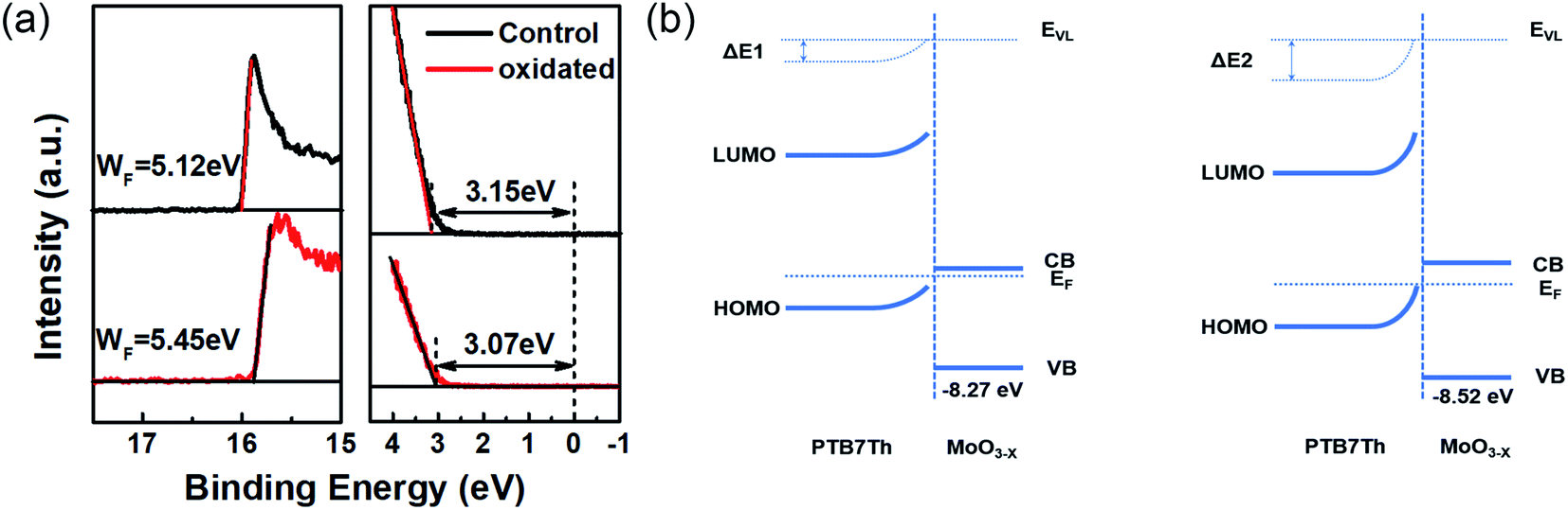 | ||
| Fig. 5 (a) UPS spectra of MoOx films measured before and after air annealing; (b) energy band diagram at PTB7-Th/MoOx interfaces for MoOx as-deposited (left) and post-annealed (right). | ||
To further understand how post-annealing affects charge extraction in devices, transient photocurrent (TPC) measurements were carried out from PSCs as-prepared and post-annealed in air. As Fig. 6(a) shows, the transients of post-annealed devices decay more quickly. The characteristic time was decreased from 4.3 μs to 2.7 μs. The hole mobilities were also measured by SCLC method. We fabricated hole-only devices with configuration of ITO/PEDOT:PSS/PTB7-Th:PC71BM/MoOx/Ag and measured the J–V curves which is shown in Fig. 6(b) on a semilogarithmic scale. The post-annealed devices exhibit higher charge transport efficiency. After air annealing, the hole mobility was increased from 1.17 × 10⁻⁴ to 2.95 × 10⁻⁴. These results indicate that carriers can be better transported out of devices by using post-annealing treatment, in agreement with the XPS and UPS results.
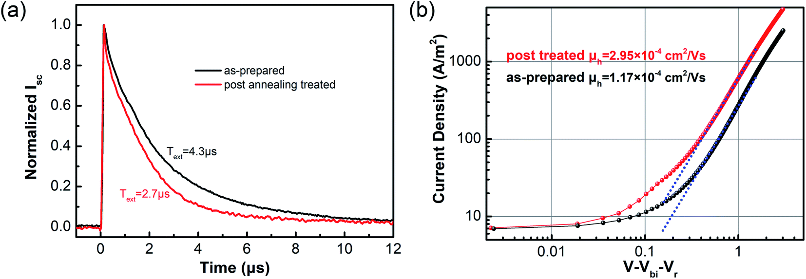 | ||
| Fig. 6 (a) The normalized TPC curves of PTB7-Th-based PSCs with as-prepared and post-annealing treated MoOx; (b) dark J–V curves of hole-only devices with as-prepared and post-annealing treated MoOx. | ||
AFM was employed to study the effect of post-annealing on surface morphology. Fig. 7 shows the AFM images of MoOx surface of as-deposited and air-annealed devices. All the films show uniform and finely intermixed domains, indicating highly blending of phase in active layer. Large donor–acceptor interfaces can be provided for exciton dissociation. Notably, the post-annealed devices exhibit smoother MoOx surface. The mean square surface roughness (Rq) was decreased from 0.91 to 0.76 after post-annealing. The smooth surface is favorable to contact with anode and facilitate charge transport, which may be another reason for the improved performance of post-annealed devices.
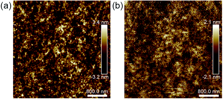 | ||
| Fig. 7 AFM height images of (a) as-deposited and (b) air-annealed MoOx surface. | ||
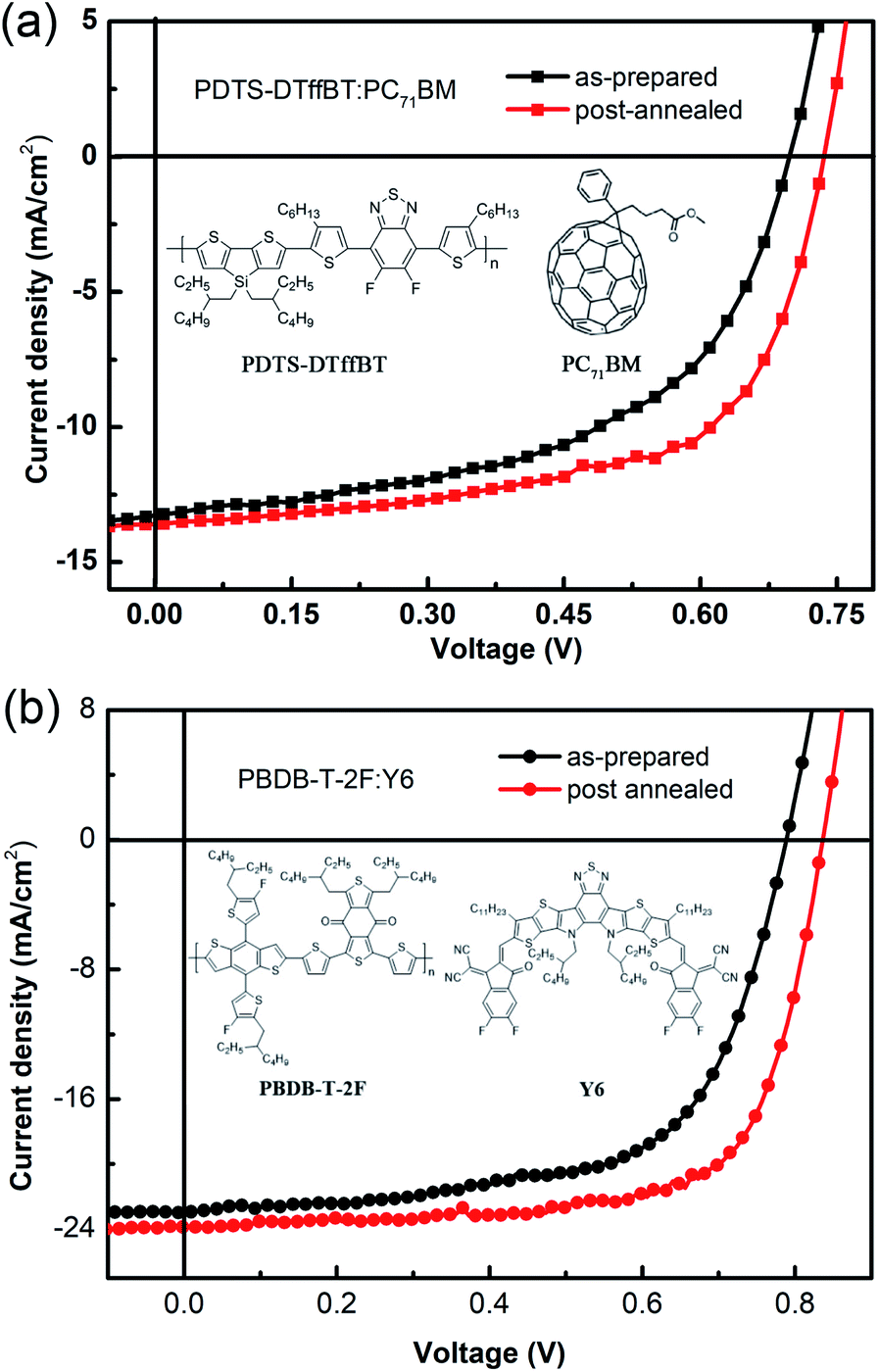
In addition, to demonstrate the universal applicability of the air annealing method, we also used PDTS–DTffBT, which we reported before,35,36 as polymer donor to fabricated PSCs and test the effect. The chemical structure of the materials and the J–V curves are showed in Fig. 8(a) and the photovoltaic data are summarized in Table 2. When the PSCs performed with post annealing treatment, the VOC and FF were improved markedly, and the JSC increased slightly, which are the same with the PTB7-Th cases. This suggests that the method may also be applied to PSCs with other polymer donors. Noticing the advanced performance achieved by non-fullerene acceptors, such as the most representative Y6,37–39 we also used the post-air annealing strategy on Y6-based non-fullerene solar cells. PSC devices using PBDB-T-2F as donor and Y6 as acceptor were fabricated. Fig. 8(b) shows the J–V curves and the data are also listed in Table 2. The results show that the post-air annealing strategy is still effective to improve photovoltaic efficiency in Y6 based non-fullerene solar cells, specially for the FF and VOC. The enhancement percentage is even greater in these high-efficiency devices. This is probably because the efficient PBDB-T-2F:Y6 active layers can produce more free carriers and are therefore more sensitive to interfacial energy level mismatch and low efficiency charge extraction.
 | ||
| Fig. 8 J–V curves of the as-prepared and post air-annealed PSCs based on (a) PDTS–DTffBT/PC71BM and (b) PBDB-T-2F/Y6 and the chemical structure of the materials. | ||
| VOC (V) | JSC (mA cm−2) | FF (%) | PCE (%) | ||
|---|---|---|---|---|---|
| Max. | Aver. | ||||
| PDTS–DTffBT:PC71BM (as-prepared) | 0.69 ± 0.01 | 12.87 ± 0.37 | 53.17 ± 0.80 | 4.91 | 4.74 |
| PDTS–DTffBT:PC71BM (post-annealed) | 0.73 ± 0.01 | 13.55 ± 0.22 | 62.33 ± 0.42 | 6.25 | 6.18 |
| PBDB-T-2F:Y6 (as-prepared) | 0.79 ± 0.01 | 22.61 ± 0.24 | 62.57 ± 0.61 | 11.43 | 11.09 |
| PBDB-T-2F:Y6 (post-annealed) | 0.84 ± 0.01 | 23.72 ± 0.30 | 69.34 ± 0.52 | 14.06 | 13.65 |
Experimental
Materials
PTB7-Th were purchased from 1-Material. PC71BM were purchased from Lumtec. PBDB-T-2F and Y6 were purchased from Solarmer Materials Inc. ZnO nanoparticles40 and PDTS–DTffBT36 were synthesized according to reported literature, which is described in the ESI.† Other materials were purchased from Aldrich and used without further purification.Measurements and characterization
XPS and UPS measurements were performed using a VD Scienta R3000 photoelectron spectrometer at ultrahigh vacuum (2 × 10⁻¹⁰ mbar) with a monochromatic Al (Kα) X-ray source (1486.6 eV) and a monochromatic He (Iα) source (21.22 eV), respectively.TPC measurements were performed using Continuum Minilete TM Nd:YAG laser to shot a 10 ns 532 nm laser pulse with the energy flux of 96.8 μJ cm−2. The laser pulse irradiated through the devices kept at short circuit and the photocurrent was recorded on an oscilloscope (Tektronix MSO 4054) by measuring the voltage drop over a 50 ohm sensing resistor in series with the solar cell.
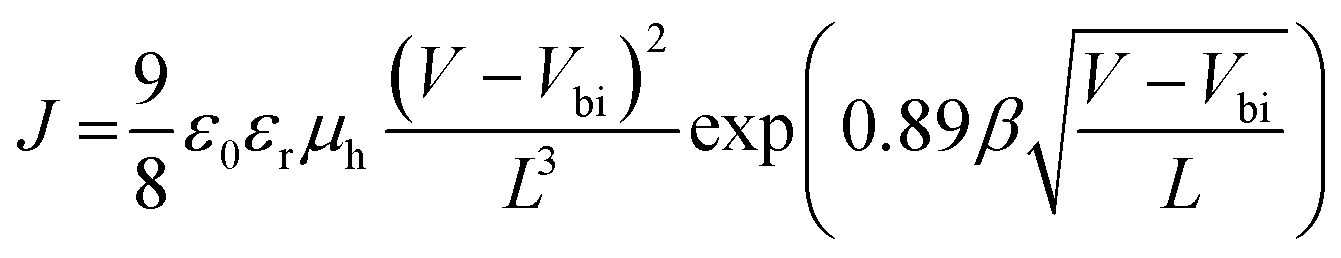
SCLC measurements were performed using hole-only devices with configuration of ITO/PEDOT:PSS/PTB7-Th:PC71BM/MoOx/Ag. The hole mobilities were calculated by fitting the resulting curves to a space-charge-limited form where SCLC can be described by:
AFM images were obtained using Veeco Dimension 3100 instrument working at tapping mode.
MoOx HTL and PSCs fabrication and characterization
The PSCs were fabricated with inverted structure of ITO/ZnO/active layer/MoOx/Al. Firstly, patterned ITO substrates (15 Ω Sq−1) were cleaned by ultrasonic using detergent, deionized water, acetone, and isopropyl alcohol sequentially. Then the substrates were fast dried by nitrogen flow followed by UV–ozone treatment for 10 min. After that ZnO nanoparticles dispersion were spin-coated at 3000 rpm for 30 s. The substrates were transferred into muffle furnace and low temperature sintered at 150 °C for 1 hour in air atmosphere. The active layer was prepared in a nitrogen-filled glove box (water and oxygen content less than 0.5 ppm). The PTB7-Th/PC71BM active layer was prepared by dissolving PTB7-Th and PC71BM with weight ratio of 1![[thin space (1/6-em)]](https://www.rsc.org/images/entities/char_2009.gif) :1.5 in chlorobenzene/1,8-diiodooctane mixed solvent (97:3 v/v) with the polymer concentration of 10 mg mL−1 and spin coating the blend solution onto the ZnO layer at 3000 rpm for 30 s. The PDTS–DTffBT/PC71BM active layer was prepared by dissolving PDTS–DTffBT and PC71BM with weight ratio of 1:2 in chlorobenzene/1,8-diiodooctane mixed solvent (97:3 v/v) with the polymer concentration of 10 mg mL−1 and spin coating the blend solution at 1200 rpm for 50 s. The PBDB-T-2F/Y6 active layer was prepared by dissolving PBDB-T-2F and Y6 with weight ratio of 1:1.2 in chloroform/1-chloronaphthalene mixed solvent (99.5:0.5 v/v) with the polymer concentration of 16 mg mL−1 and spin coating the blend solution at 3000 rpm for 30 s.37 The MoOx HTL (6 nm thick) was prepared using vacuum vapor phase deposition method. The vacuum of the evaporation chamber should be controlled below 1 × 10⁻⁵ pa. After the deposition of MoOx, the substrates with ZnO layer, active layer and MoOx layer was post-annealed at 90 °C for 10 min in air atmosphere on a hot plate. 90 nm Al cathode was vacuum evaporated to finish the fabrication. For the control devices, the post-air annealing process was skipped, the Al cathode was evaporated immediately after the deposition of MoOx layer. 10 optimized devices were fabricated and measured for each condition.
:1.5 in chlorobenzene/1,8-diiodooctane mixed solvent (97:3 v/v) with the polymer concentration of 10 mg mL−1 and spin coating the blend solution onto the ZnO layer at 3000 rpm for 30 s. The PDTS–DTffBT/PC71BM active layer was prepared by dissolving PDTS–DTffBT and PC71BM with weight ratio of 1:2 in chlorobenzene/1,8-diiodooctane mixed solvent (97:3 v/v) with the polymer concentration of 10 mg mL−1 and spin coating the blend solution at 1200 rpm for 50 s. The PBDB-T-2F/Y6 active layer was prepared by dissolving PBDB-T-2F and Y6 with weight ratio of 1:1.2 in chloroform/1-chloronaphthalene mixed solvent (99.5:0.5 v/v) with the polymer concentration of 16 mg mL−1 and spin coating the blend solution at 3000 rpm for 30 s.37 The MoOx HTL (6 nm thick) was prepared using vacuum vapor phase deposition method. The vacuum of the evaporation chamber should be controlled below 1 × 10⁻⁵ pa. After the deposition of MoOx, the substrates with ZnO layer, active layer and MoOx layer was post-annealed at 90 °C for 10 min in air atmosphere on a hot plate. 90 nm Al cathode was vacuum evaporated to finish the fabrication. For the control devices, the post-air annealing process was skipped, the Al cathode was evaporated immediately after the deposition of MoOx layer. 10 optimized devices were fabricated and measured for each condition.
Conclusions
We have demonstrated that the oxidation state and WF of MoOx buffer layer can be raised by post-air annealing strategy, which provide stronger driving force for charge transport. Better photovoltaic performance can be achieved by PSCs based on the post-air annealed MoOx HTL. For metal oxide semiconductor materials as buffer layer, MoOx films with higher oxidation state is more in line with the principle of selection. The results provide theoretical and experimental support for improving the performance of optoelectronic devices.Conflicts of interest
There are no conflicts to declare.Acknowledgements
This work was supported by National Natural Science Foundation of China (Grant No. 62004081, 11904126), Science and Technology Project of Jilin Provincial Education Department (Grant No. JJKH20180550KJ, JJKH20200250KJ), Scientific and Technological Innovation Development Plan Project of Jilin City (Grant No. 201831777), Scientific Research Project of Jilin Institute of Chemical Technology (Grant No. 2018016, 2021004).References
- G. Yu, J. Gao, J. C. Hummelen, F. Wudl and A. J. Heeger, Science, 1995, 270, 1789–1791 CrossRef CAS.
- J. Brabec, N. S. Saricifici and J. C. Hummelen, Adv. Funct. Mater., 2001, 11, 15–26 CrossRef.
- M. Helgesen, R. Søndergaard and F. C. Krebs, J. Mater. Chem., 2010, 20, 36–60 RSC.
- F. C. Krebs, J. Fyenbo and M. Jørgensen, J. Mater. Chem., 2010, 41, 8994–9001 RSC.
- Y. Sun, Y. Zhang, Q. Liang, Y. Zhang, H. Chi, Y. Shi and D. Fang, RSC Adv., 2013, 30, 11925–11934 RSC.
- L. Zhan, S. Li, X. Xia, Y. Li, X. Lu, L. Zuo, M. Shi and H. Chen, Adv. Mater., 2021, 33, 2007231 CrossRef CAS PubMed.
- T. Zhang, C. An, P. Bi, Q. Lv, J. Qin, L. Hong, Y. Cui, S. Zhang and J. Hou, Adv. Energy Mater., 2021, 2101705 CrossRef CAS.
- Q. Liu, Y. Jiang, K. Jin, J. Qin, J. Xu, W. Li, J. Xiong, J. Liu, Z. Xiao, K. Sun, S. Yang, X. Zhang and L. Ding, Sci. Bull., 2020, 65, 272–275 CrossRef CAS.
- H. J. Son, F. He, B. Carsten and L. Yu, J. Mater. Chem., 2011, 21, 18934–18945 RSC.
- R. K. Pai, T. N. Ahipa and B. Hemavathi, RSC Adv., 2016, 6, 23760–23774 RSC.
- R. K. Gupta, R. Garai, M. Hossain, M. A. Afroz, D. Kalita and P. Krishnanlyer, J. Mater. Chem. C, 2021, 9, 8746–8775 RSC.
- V. Malytskyi, J. J. Simon, L. Patrone and J. M. Raimundo, RSC Adv., 2015, 5, 354–397 RSC.
- P. Ma, C. Wang, S. Wen, L. Wang, L. Shen, W. Guo and S. Ruan, Sol. Energy Mater. Sol. Cells, 2016, 155, 30–37 CrossRef CAS.
- O. Adebanjo, P. P. Maharjan, P. Adhikary, M. Wang, S. Yang and Q. Qiao, Energy Environ. Sci., 2013, 6, 3150–3170 RSC.
- Z. Shi, Y. Bai, X. Chen, R. Zeng and Z. Tan, Sustainable Energy Fuels, 2019, 3, 910–934 RSC.
- E. D. Gomez and Y. L. Loo, J. Mater. Chem., 2010, 20, 6604–6611 RSC.
- G. Li, C. W. Chu, V. Shrotriya, J. Huang and Y. Yang, Appl. Phys. Lett., 2006, 88, 253503 CrossRef.
- M. Campoy-Quiles, T. Ferenczi, T. Agostinelli, P. G. Etchegoin, Y. Kim, T. D. Anthopoulos, P. N. Stavrinou, D. D. C. Bradley and J. Nelson, Nat. Mater., 2008, 7, 158–164 CrossRef CAS PubMed.
- Z. He, C. Zhong, S. Su, M. Xu, H. Wu and Y. Cao, Nat. Photonics, 2012, 6, 591–595 CrossRef.
- R. Po, C. Carbonera, A. Bernardi and N. Camaioni, Energy Environ. Sci., 2011, 4, 285–310 RSC.
- Z. Liang, Q. Zhang, L. Jiang and G. Cao, Energy Environ. Sci., 2015, 8, 3442–3476 RSC.
- Y. Ono, T. Akiyama, S. Banya, D. lzumoto, J. Saito, K. Fujita, H. Sakaguchi, A. Suzuki and T. Oku, RSC Adv., 2014, 4, 34950–34954 RSC.
- R. Lampande, G. W. Kim, R. Pode and J. H. Kwon, RSC Adv., 2014, 4, 49855–49860 RSC.
- V. Shrotriya, G. Li, Y. Yao, C. W. Chu and Y. Yang, Appl. Phys. Lett., 2006, 88, 073508 CrossRef.
- M. G. Varnamkhasti, H. R. Fallah, M. Mostajaboddavati, R. Ghasemi and A. Hassanzadeh, Sol. Energy Mater. Sol. Cells, 2012, 98, 379–384 CrossRef.
- J. Meyer, S. Hamwi, M. Kröger, W. Kowalsky, T. Riedl and A. Kahn, Adv. Mater., 2012, 24, 5408–5427 CrossRef CAS PubMed.
- E. Itoh and S. Nakagoshi, Jpn. J. Appl. Phys., 2014, 53, 502–503 CrossRef.
- F. Liu, S. Shao, X. Guo, Y. Zhao and Z. Xie, Sol. Energy Mater. Sol. Cells, 2010, 94, 842–845 CrossRef CAS.
- J. Meyer, S. Hamwi, M. Kröger, W. Kowalsky, T. Riedl and A. Kahn, Adv. Mater., 2012, 24, 5408–5427 CrossRef CAS PubMed.
- K. H. Wong, K. Ananthanarayanan, J. Luther and P. Balaya, J. Phys. Chem. C, 2012, 116, 16346–16351 CrossRef CAS.
- W. Zhao, D. Qian, S. Zhang, S. Li, O. Inganas, F. Gao and J. Hou, Adv. Mater., 2016, 28, 4734–4739 CrossRef CAS PubMed.
- T. S. Sian and G. B. Reddy, Sol. Energy Mater. Sol. Cells, 2004, 82, 375–386 CrossRef CAS.
- P. C. Kao, Z. H. Chen, H. E. Yen, T. H. Liu and C. L. Huang, Jpn. J. Appl. Phys., 2018, 57, 03DA04 CrossRef.
- J. Liang, F. S. Zu, L. Ding, M. F. Xu, X. B. Shi, Z. K. Wang and L. S. Liao, Appl. Phys. Express, 2014, 7, 111601 CrossRef.
- P. Ma, S. Wen, C. Wang, W. Guo, L. Shen, W. Dong, J. Lu and S. Ruan, J. Phys. Chem. C, 2016, 120, 19513–19520 CrossRef CAS.
- S. Wen, C. Wang, P. Ma, Y. Zhao, C. Li and S. Ruan, J. Mater. Chem. A, 2015, 3, 13794–13800 RSC.
- J. Yuan, Y. Zhang, L. Zhou, G. Zhang, H. L. Yip, T. K. Lau, X. Lu, C. Zhu, H. Peng, P. A. Johnson, M. Leclerc, Y. Cao, J. Ulanski, Y. Li and Y. Zou, Joule, 2019, 3, 1140–1151 CrossRef CAS.
- Y. Lin, B. Adilbekova, Y. Firdaus, E. Yengel, H. Faber, M. Sajjad, X. Zheng, E. Yarali, A. Seitkhan, O. M. Bakr, A. El-Labban, U. Schwingenschlögl, V. Tung, I. McCulloch, F. Laquai and T. D. Anthopoulos, Adv. Mater., 2019, 31, 1902965 CrossRef CAS PubMed.
- X. Guo, Q. Fan, J. Wu, G. Li, Z. Peng, W. Su, J. Lin, L. Hou, Y. Qin, H. Ade, L. Ye, M. Zhang and Y. Li, Angew. Chem., Int. Ed., 2021, 60, 2322–2329 CrossRef CAS PubMed.
- C. Wang, C. Li, S. Wen, P. Ma, Y. Liu, R. C. I. Mackenzie, W. Tian and S. Ruan, J. Mater. Chem. A, 2017, 5, 3995–4002 RSC.
- W. Liu, P. Ma, J. Xu, C. Wang, C. Wang, M. Qu and S. Wen, Phys. Status Solidi A, 2021, 218, 2000650 CrossRef CAS.
Footnote |
| † Electronic supplementary information (ESI) available. See DOI: 10.1039/d1ra06929b |
| This journal is © The Royal Society of Chemistry 2021 |