
 Open Access Article
 This Open Access Article is licensed under a Creative Commons Attribution-Non Commercial 3.0 Unported Licence
UV electroluminescence emissions from high-quality ZnO/ZnMgO multiple quantum well active layer light-emitting diodes†
Shanshan Chen abc,
Tengrun Zhana,
Xinhua Pan*cde,
Haiping Hecd,
Jingyun Huangcd,
Bin Lucd and
Zhizhen Yecde
abc,
Tengrun Zhana,
Xinhua Pan*cde,
Haiping Hecd,
Jingyun Huangcd,
Bin Lucd and
Zhizhen Yecde
aSchool of Materials and Energy, Guangdong University of Technology, Guangzhou 510006, People's Republic of China
bGuangdong Provincial Key Laboratory of Information Photonics Technology, Guangzhou 510006, People's Republic of China
cState Key Laboratory of Silicon Materials, Zhejiang University, Hangzhou 310027, People's Republic of China. E-mail: panxinhua@zju.edu.cn
dSchool of Materials Science and Engineering, Cyrus Tang Center for Sensor Materials and Applications, Zhejiang University, Hangzhou 310027, People's Republic of China
eWenzhou Key Laboratory of Novel Optoelectronic and Nano Materials, Institute of Wenzhou, Zhejiang University, Wenzhou 325006, P. R. China
First published on 6th December 2021
Abstract
5-period ZnO/Zn0.9Mg0.1O multiple quantum wells (MQWs) were employed as active layers to fabricate the p-GaN/MQWs/n-ZnO diode by molecular beam epitaxy. It exhibited an efficient UV emission around 370 nm at room temperature. Calculated band structures and carrier distributions showed that electrons were restricted to overflow to the p-type layer, and carriers were confined in the high-quality MQWs well layer.
Introduction
Ultraviolet (UV) light-emitting diodes (LEDs) and laser diodes (LDs) have attracted much interest for their potential use in long-lifetime solid-state lighting, high-density information storage, detection and secure communication. Fueled and fanned by the broad application prospects, intensive research efforts have been made on wide-bandgap semiconductors to realize efficient UV LEDs and LDs.1–3 Among the available wide-bandgap semiconductors, ZnO with a wide bandgap (3.37 eV) and large exciton binding energy (60 meV) has turned out to be a promising candidate for creating high-efficiency and low-threshold light-emitting devices, which will operate at room or higher temperatures.4,5 In order to realize modern light-emitting devices, two important requirements should be satisfied: one, p-type and n-type materials for carrier injection, and the other is a modulation of bandgap to create multiple quantum wells (MQWs) for carrier recombination.6 Unipolar doping seems to be a common issue in wide bandgap semiconductors, and ZnO is no exception. ZnO is easily doped to n-type, but it is difficult to dope to a p-type. Difficulty in p-type ZnO has always been the obstacle to fabricate homojunction light-emitting devices. The latter requirement has been demonstrated by alloying. Compared to other alloys, Zn1−xMgxO is considered a suitable barrier material for ZnO MQWs.7–9 The growth and optical properties of ZnO/Zn1−xMgxO MQWs have been widely studied.10–15 Electrically pumped light emission or lasing actions in ZnO/Zn1−xMgxO MQWs is scarce but highly desirable. Much more attention should be drawn to ZnO/Zn1−xMgxO MQWs working as an active layer in LEDs or LDs. Research on homojunction LEDs or LDs using ZnO/Zn1−xMgxO MQWs as an active layer is limited by p-type doping and growth of high-quality MQWs.16–19 While p-type doping of ZnO is under intensive study, the heterojunction structure can be adopted to realize ZnO/Zn1−xMgxO MQW active layer devices. However, there have been no relevant reports about such heterojunction devices. Heteroepitaxy and interface issues make it difficult. In this work, p-GaN/n-ZnO LEDs employing a ZnO/Zn1−xMgxO MQW active layer have been demonstrated, for the reason that p-GaN is commercially available and GaN has the same crystalline structure with closely matched lattice constants compared to ZnO.20–22 Moreover, a record high internal quantum efficiency of ZnO/ZnMgO MQWs is 61% at 300 K is obtained by using GaN/Al2O3 as a substrate, which has been reported in our latest research.23 We investigated the optical properties and structures of ZnO/Zn1−xMgxO MQWs to obtain high-quality MQW structures. The effect of MQWs on the performance of LEDs has been analyzed and electrically pumped UV light emission has been achieved. The efficient UV emission is derived from the ZnO/ZnMgO MQW active layer due to the obvious quantum confinement effect.Experimental details
ZnO/Zn1−xMgxO MQWs were grown on commercially available p-GaN/Al2O3 templates via the plasma-assisted molecular beam epitaxy (MBE) technique. Elemental zinc (6N grade), magnesium (6N grade) and oxygen radio frequency plasma (O2 gas, 6N grade) were used as sources. Prior to the growth, thermal cleaning of p-GaN/Al2O3 templates was carried out in the preparation chamber at 300 °C for several hours, followed by in the growth chamber at 700 °C for 30 min to produce a clean surface. For better film crystallinity and a flatter surface, a thin low-temperature ZnO layer was deposited as a buffer layer. Zn1−xMgxO films or 5-period ZnO/Zn1−xMgxO MQWs were subsequently grown on the buffer layer at 650 °C. The Zn cell temperature, oxygen flow rate and radiofrequency excitation power were fixed at 250 °C, 1.0 standard cubic centimetres per minute (sccm) and 300 W, respectively. Mg cell temperature was varied at 340 °C, 345 °C, and 350 °C to obtain Zn1−xMgxO films with different Mg contents. Mg cell temperature was fixed at 350 °C to fabricate 5-period ZnO/Zn1−xMgxO MQWs. The thickness of the Zn1−xMgxO barrier layer was 10 nm, and the thickness of the ZnO well layer was varied from 2 nm to 8 nm by controlling deposition time. The details about the determination of thickness are available in the ESI file.† For the fabrication of heterojunction diodes, a low-temperature ZnO buffer layer, 10 nm thick Zn1−xMgxO layer, 5-period ZnO/Zn1−xMgxO MQWs and undoped ZnO layer were deposited on p-GaN/Al2O3 templates in a sequence. For comparison, another heterojunction sample without MQWs was also prepared under the same conditions. Bilayer Ni/Au electrode and Sn electrode were used as the contacts for p-GaN and n-ZnO layers, respectively.The Mg content was determined by X-ray photoelectron spectroscopy (XPS). The crystalline structure was analyzed by X-ray diffraction (XRD) with Cu Kα radiation (λ = 1.54056 Å). The electrical properties of the p-GaN film were investigated by the van der Pauw method with Hall measurements, and it showed a hole concentration of 5.30 × 1017 cm−3 and Hall mobility of 14.7 cm2 V−1 s−1. Photoluminescence (PL) measurements were used to analyse the optical properties of the single-layer films and MQWs, which employed a 25 mW He–Cd laser operating at a wavelength of 325 nm as the excitation source and performed on an FLS920 (Edinburgh Instruments) fluorescence spectrometer. The surface morphology and roughness of MQWs were characterized by atomic force microscopy (AFM). The elemental depth profile of the MQWs was investigated using secondary ion mass spectroscopy (SIMS) measurements. The electrical properties of heterojunction diodes were studied by current–voltage (IV) measurements using a semiconductor parameter analyzer (Agilent E5270B). Electroluminescence (EL) measurements were performed using a PL instrument, and a continuous-current power source was used to excite the diodes. All measurements were performed at room temperature. The simulations of carrier distribution, energy band structures and EL spectra for ZnO MQW LEDs were made with the APSYS package from Crosslight Software Inc. (technical details about the simulation are available in ESI†).
Results and discussions
In order to fabricate high-quality ZnO/Zn1−xMgxO MQWs on GaN substrates, the heteroepitaxial Zn1−xMgxO films with varied Mg contents were studied. Mg contents were determined as 0 (refers to ZnO), 4%, 8%, and 10%. Pure c-plane oriented Zn1−xMgxO films were grown on c-plane GaN/Al2O3 templates, as shown in Fig. 1(a). The crystalline quality of Zn1−xMgxO films was characterized by high-resolution X-ray diffraction (HRXRD).24 In general, the full width at half maximum (FWHM) value of (002) ω-rocking curve is related to screw threading dislocations (TDs), while FWHM of (102) ω-rocking curve is responsible for the edge TDs, which is usually dominant in the epitaxial growth such as GaN and ZnO. Here, Fig. 1(b) shows the XRD ω-rocking curves of GaN (002) diffraction peak for GaN/Al2O3 template and ZnO (002) diffraction peak for Zn1−xMgxO films. Due to the matched lattice constants with GaN, 2θ for ZnO and GaN (002) are very close, which are 34.42° and 34.56°, respectively. The peaks are fitted by pseudo-Voigt function. FWHM values of the diffraction peaks from Zn1−xMgxO samples are almost equal to those from GaN/Al2O3 template, as shown in Table S1 (see in ESI).† The signal from Zn1−xMgxO (002) diffraction peak is covered by GaN (002) diffraction. Although, the (002) diffraction peaks from Zn1−xMgxO layers cannot be recognized, it is inferred that FWHM values of Zn1−xMgxO films (002) diffraction peak are almost equal to or even less than the fitted value. As well, XRD ω-rocking curves of Zn1−xMgxO (102) diffraction peak were measured, as shown in Fig. 1(c). There are two recognizable diffraction peaks for each sample. The FWHM values of the two peaks are about 600 arcsec and 300 arcsec, as shown in Table S1.† Standard 2θ values of (102) diffraction for ZnO and GaN are 47.54°, and 48.08°, respectively. It is known that peak position goes to the left as diffraction angles are smaller. Thus, the left broadened peak is originated from Zn1−xMgxO for its slightly smaller diffraction angle. Moreover, the right peak shows very close FWHM value as the single peak from the GaN sample (about 300 arcsec), which also confirms that the right one is corresponding to the GaN layer, and the left broad one originates from the Zn1−xMgxO layer. The relatively small FWHM values indicate low defect density in epitaxial films.24 Fig. 1(d) shows room-temperature PL spectra of Zn1−xMgxO films with different Mg contents. It is noteworthy that the dominant near-band-edge (NBE) emission peak shifts monotonously from 378 nm to 362 nm as Mg content increases from 0 to 0.10. The blue shift behavior is attributed to the increase of bandgap with Mg incorporation. In the type-I band structured ZnO/Zn1−xMgxO junction, the increasing bandgap of Zn1−xMgxO leads to a larger barrier height for both electrons and holes. Henceforth, the MQWs are referred to as ZnO/Zn0.9Mg0.1O MQWs in the following text. | ||
| Fig. 1 (a) XRD patterns in θ–2θ geometry of Zn1−xMgxO films with different Mg content grown on p-GaN/Al2O3 templates. (b) XRD ω-rocking curves of GaN (002) and ZnO (002) diffraction peaks for GaN/Al2O3 template and Zn1−xMgxO films grown on GaN/Al2O3 templates, respectively. (c) XRD ω-rocking curves of GaN (102) and ZnO (102) diffraction peak for GaN/Al2O3 template and Zn1−xMgxO films grown on GaN/Al2O3 templates, respectively. (d) Room-temperature PL spectra of the Zn1−xMgxO films. | ||
The well-width of MQWs are varied from 2 nm to 8 nm by controlling deposition time. These MQWs are labeled as W2, W4, W6 and W8, respectively. The PL properties of MQWs with different well widths are investigated. The p-GaN film, single-layer ZnO and Zn0.9Mg0.1O films deposited under the same growth conditions are taken for comparison. Fig. 2(a) shows the normalized room-temperature PL spectra. The p-GaN film exhibits an emission around 435 nm (red dash line), which is ascribed to transitions from the conduction band or unidentified shallow donors to Mg acceptor levels in the p-GaN film. Single-layer ZnO film exhibits a narrow emission at 378 nm (black dash line), which is attributed to the NBE emission of ZnO. Single-layer Zn0.9Mg0.1O film exhibits a narrow emission at 362 nm and a weak visible region emission started from 450 nm to 640 nm (blue dash line). The narrow emission at 362 nm is also attributed to the NBE emission of Zn0.9Mg0.1O, and the emission started from 450 nm to 640 nm is ascribed to deep-level defects related to the emission of Zn0.9Mg0.1O. In order to realize efficient output, the defects related to emissions should be avoided. Each MQWs also shows a dominant UV emission located between 366 nm to 373 nm and a weak visible region emission also started from 450 nm to 640 nm (solid lines). No separate emission from a single ZnO well layer (black dash line) or Zn0.9Mg0.1O barrier layer (blue dash line) is observed for the MQWs. The emission from the lower layer p-GaN templates is undetectable either. These UV emissions exhibit blue-shift compared with the emission from ZnO film. It indicates that emissions of MQWs are attributed to the recombination of the localized exciton in the ZnO well and blue-shift is due to the quantum confinement effect (QCE).14,25 The recombination of the localized exciton in the ZnO well layer and undetected emission from the Zn0.9Mg0.1O barrier layer both certificate the efficient carrier injection from barrier to well. UV emissions varied monotonically from 373 nm to 366 nm as the MQWs well width reduced from 8 nm to 2 nm, as shown in Fig. 2(b). Here, well-width at 0 represents Zn0.9Mg0.1O. The peak position is gradually shifted to higher energy with a narrower well-width, as shown in Fig. 2(b), which is expected for a more notable QCE.9,26 More notable QCE leads to more efficient carrier injection to well, which is very desirable for efficient carrier recombination. It seems that the smaller well-width, the better. However, the PL performance starts to deteriorate with an enhanced defect emission from 450 nm to 640 nm when the well-width decreased to 2 nm, as shown in Fig. 2(a). It reveals that well-widths of 4 nm (W4) and 6 nm (W6) are better, by taking the overall consideration of QCE and PL performance.
 | ||
| Fig. 2 (a) The room-temperature PL spectra of the p-GaN film, ZnO film, Zn0.9Mg0.1O film and the ZnO/Zn0.9Mg0.1O MQWs with well-width of 2 nm, 4 nm, 6 nm, and 8 nm. (b) The peak position of NBE emissions versus well-width. (c) AFM image for sample W6. (d) SIMS depth profiles of Mg, Zn, and Ga in the 5-period ZnO/Zn0.9Mg0.1O MQWs. | ||
In addition, surface flatness is also the key indicator to evaluate the quality of MQWs. After testing the surface roughness, we found that the surface of W6 is very flat, and the root mean square (rms) surface roughness is only 0.6 nm, as shown in Fig. 2(c). A deep analysis of elements depth profiles at the interfaces for W6 is carried out by SIMS, as shown in Fig. 2(d). In the top epitaxial layer, five sharp peaks about Mg can be clearly resolved, which is highly consistent with the structure of the 5-period MQWs. It suggests the sharp interfaces between the well and barrier layers. Processed through the whole high-temperature growth, the interdiffusion of Mg is only slight. The low-temperature ZnO buffer layer between MQWs and substrate can also be recognized when the etching time increases to 5000 s. The interface between the epitaxial layer and p-GaN substrate can be confirmed from the profiles of Zn and Ga when the etching time increases to 6000 s. The smooth surface ensures good interfaces. Hence, considering QCE, PL performance and interface quality, the well width of 6 nm is very suitable.
Based on these optimized parameters, 5-period ZnO/Zn0.9Mg0.1O MQWs with a well width of 6 nm and a barrier width of 10 nm were employed to form the heterojunction diode. The diagram of the p-GaN/MQWs/n-ZnO diode is shown in Fig. 3(a). IV curves of the Ni/Au electrode on the p-GaN layer and the Sn electrode on the n-ZnO layer are shown in Fig. 3(b). Both Ni/Au-contact to the p-type GaN layer and Sn-contact to n-type ZnO layer show good ohmic behavior. The IV characteristic of the diode is shown in Fig. 3(c). The device exhibits well rectification with a turn-on voltage of 3.5 V, which is in good agreement with the ZnO bandgap energy of 3.37 eV. The ideal factor is about 2.5 under a low-level forward injection. Commonly, the p–n junction should have an ideal factor between 1 and 2 as per the Sah–Noyce–Shockley theory. However, referring to previous studies on GaN-based LEDs, it is shown that unipolar heterojunctions, dislocations in MQWs, as well as metal contact to p-type GaN, can increase the ideal factor to values much greater than 2.0. It is reported that low defect density GaN devices displayed improved ideal factors, which were close to 1–2. The ideal factor of 2.5 in this work is close to 2. It indicates that the recombination current is the dominant carrier transport mode. The relatively small FWHM values of Zn1−xMgxO (102) XRD ω-rocking diffraction peaks indicate low defect density in the epitaxial films in our research as shown in Fig. 1(c) and Table S1.† This low defect density is supposed to make important contributions to avoid a commonly high ideal factor as in GaN devices.
 | ||
| Fig. 3 (a) Schematic illustration of the p-GaN/MQWs/n-ZnO diode structure. (b) IV curves of the Ni/Au electrodes on the p-GaN layer (pp) and the Sn electrodes on n-ZnO layer (nn). (c) IV curve of the p-GaN/MQWs/n-ZnO diode in normal (black line) and log-scale (red line). | ||
A benchmark summary of representative n-ZnO/p-GaN LEDs is presented in Table 1. Research on ZnO/Zn1−xMgxO MQWs LEDs is very limited. All of the reported structure is n-ZnO/MQWs/p-ZnO, and their related performances are listed in Table 2. In our work, the leakage current is 1.7 mA at a reverse bias of 10 V. It is two orders of magnitude higher than that of n-ZnO/p-GaN devices as shown in Table 1. While it is comparable to the previously reported MQW devices in Table 2. It indicates that many interface defect states exist in MQW devices. This still needs further research to improve.
| Reference no. | 28 | 29 | 30 | 31 | 32 | 33 |
|---|---|---|---|---|---|---|
| a * values estimated using figures or data provided in the paper; # values, which are neither available nor can be estimated from available data. | ||||||
| Turn-on voltage (V) | 3 | 5 | −3* | 3 | 13 | 3 |
| Turn-on current (mA) | 15* | 0.003 | −0.2* | # | 0.1* | # |
| Leakage current (mA) | 0.005@3 V | 0.01@20 V | # | # | 0.003@15 V | # |
| EL detectability threshold (V) | # | 7 | −5 | 3.5 | # | 10 |
| EL detectability current (mA) | # | 0.04 | −0.5* | # | 1.8 | 1* |
| Dominant EL peak (nm) | 430 | 440 | 445, 560 | 392–420 | 393, 409, 437 | 383, 402, 430 |
| FWHM of EL peak (nm) | 25 | 50* | >50* | 34 | 36 | 24–48 |
| Origin for EL peak | p-GaN | p-GaN | p-GaN, n-ZnO | n-ZnO, p-GaN, and interface | ||
| Reference no. | 16 | 17 | 18 | 19 | This work |
|---|---|---|---|---|---|
| a * values estimated using figures or data provided in the paper; # values which are neither available nor can be estimated from available data; ELMQWs and ELPN: integrated intensity for dominant EL peak from MQWs LEDs and their corresponding p–n junction LEDs without MQWs, ELMQWs/ELPN: the relative EL intensity value of LED with MQWs compared to the LED without MQWs. | |||||
| Turn-on voltage (V) | 3.2 | 7 | 2.2 | 4* | 3.5 |
| Turn-on current (mA) | 0.02* | # | 10* | # | 0.7 |
| Leakage current (mA) | 0.1*@4 V | 4* @20 V | # | # | 1.7@10 V |
| EL detectability threshold (V) | # | # | 7 | 6.2 | 5 |
| EL detectability current (mA) | 20 | # | 50* | 20 | 1 |
| Dominant EL peak (nm) | 380 | 380 | 385 | 380* | 372, 380 |
| FWHM of EL peak (nm) | 40*@40 mA | 0.4@20 mA laser | 50* | <20* | 7, 13@20 mA |
| ELMQWs/ELPN | 1.55 | # | # | 1.22* | 16 |
Fig. 4(a) shows the EL spectra of the diode operating at forward currents from 1 mA to 22 mA. Both the UV emission at around 370 nm and deep-level emission starting from 500 nm to 725 nm are enhanced as the current injection level increases. The deep-level emission is the dominant feature at low forward currents (in the region below 13 mA), while emission around 370 nm becomes the prominent spectral feature when the current injection level is higher than 13 mA. Fig. 4(b) shows the Gaussian fitting of the EL spectrum with the current of 22 mA. It can be fitted into four peaks. Generally, the UV emission band peaking at about 370 nm is attributed to the ZnO NBE emission that originates from the recombination of localized excitons (LE) in ZnO well layers. Emissions in the visible region started from 500 nm to 725 nm are often coming from defect-related emission (DE). Both LE and DE peaks are asymmetrical. LE can be divided into two close peaks that originate from the recombination of ZnO-free and bound excitons (FE and BE). DE can be divided into two peaks located at 549 nm and 613 nm. After fitting the EL emissions at different currents, the trends of FWHM values, peak positions and integrated EL intensity for each emission with increasing injection current were studied as shown in Fig. 4(c) and (d). The peak positions of FE and BE are scarcely shifted, as the current increased, which suggests stable wavelength emission. What is more, the FWHM of FE and BE peaks are very narrow and also relatively stable as the current increases. The FWHM is only 7 nm for FE and 13 nm for BE. It shows better monochromaticity with comparison to other reports in Tables 1 and 2. While the visible region deep-level emission is a strong and wide peak as shown in Fig. 4(a). This behaviour also indicates the existence of many defect states. It shows a blueshift with the increase of current as seen in Fig. 4(a), which is believed to result from the saturation of the lowest energy levels.17 Fig. 4(d) indicates that emissions from FE and BE are rapidly increasing and the growth of DE occurs more and more slowly as the injection current increases. It suggests that the recombination of LE from MQWs is becoming more efficient.
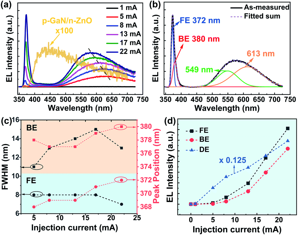 | ||
| Fig. 4 (a) EL spectra of the p-GaN/MQWs/n-ZnO diode under different forward currents and EL spectrum of p-GaN/n-ZnO diode under the forward current of 22 mA. Note that the EL intensity for p-GaN/n-ZnO diode has been magnified by 100 times. (b) Gaussian fitting of the EL spectrum with current of 22 mA. FE: recombination of ZnO free excitons; BE: recombination of ZnO bound excitons. (c) FWHM values and peak positions of emission peaks from FE and BE plotted as a function of injection current. (d) Integrated EL intensity of FE, BE and DE emissions plotted as a function of injection current. | ||
For the purpose of better understanding the EL results and the effect of MQWs on the performance of the diode, the EL spectrum of the p-GaN/n-ZnO heterojunction diode operated at forward currents of 22 mA is also displayed in Fig. 4(a). The diode without MQWs shows a weak emission around 450 nm, which is very similar to the PL emission from the p-GaN layer shown in Fig. 2(a). It indicates that the emissions are from the GaN layer, while that from the ZnO layer is undetectable. This weaker and broader emission means low efficiency and poor monochromaticity, which is detrimental to device applications. This is a common issue for p-GaN/n-ZnO heterojunction diodes according to Table 1.27–33 It is because electrons in the ZnO layer with higher mobility are more easily drifted into GaN and recombined with holes to form the emission. In that case, p-GaN does not supply holes to ZnO, on the contrary, ZnO acts as an electron source for the p-GaN layer. Finally, the advantage of the large exciton binding energy of ZnO is not fully exploited in the p-GaN/n-ZnO heterojunction diode. As for the diode with MQWs, obviously, the peak located around 370 nm is not derived from the p-GaN layer. It shows a blue-shift from the PL emission of n-type ZnO (located at 378 nm in Fig. 2(a)), which is related to the QCE. Therefore, it is determined that this UV emission originates from the localized-exciton recombination in the MQW active layer. The EL spectrum is detected at a bias as low as 5 V for our device. This threshold is relatively low in comparison to that in the previously reported LED devices, as shown in Tables 1 and 2. Compared to the LED without MQWs, the EL emission of LED with MQWs has more efficiency. According to the relative EL intensity values (ELMQWs/ELPN) in Table 2, the emission with MQWs increases 16 times comparing with bare p–n junction. This is a remarkable improvement in contrast to the values of other devices as shown in Table 2.
To further understand the carrier recombination process in LEDs, the carrier distribution, energy band structures and EL spectra for ZnO MQW LEDs were calculated using the APSYS package. The LED structures in the simulation are shown in Fig. S2† and the related electrical properties of films are listed in Table S2 (see in ESI).† Fig. 5(a) and (b) show the conduction and valence band energy diagrams at 25 mA for the p-GaN/n-ZnO diode and p-GaN/MQWs/n-ZnO diode, respectively. There are energy barriers for both electrons and holes in the p-GaN/n-ZnO diode. Fig. 5(c) and (d) show the distribution of electron and hole concentrations in each region of the two diodes, respectively. As shown in Fig. 5(c), carrier diffusion concentrations decrease rapidly with a longer electron diffusive distance. It finally results in a weak emission from the p-type layer in the p-GaN/n-ZnO diode, as shown in Fig. 5(e). Different from that, in the p-GaN/MQWs/n-ZnO diode, the MQWs blocks the overflow of electrons to the p-type region and accumulates both electrons and holes in the well layers, leading to a high hole concentration in the MQWs. Both hole and electron concentrations increase more than an order of magnitude in the quantum well adjacent to the p-type layer in the p-GaN/MQWs/n-ZnO diode, as shown in Fig. 5(d), compared to the carrier concentrations at the interface in the p-GaN/n-ZnO diode. Due to the blocking of electron overflow to the p-type layer and confining of carriers in ZnO well layers, the efficiency of UV emission (the intensity is nearly two orders of magnitude to the intensity of emission from p-GaN/n-ZnO diode) from ZnO well is obtained as shown in Fig. 5(f). By comparing the performance of the two diodes, it is found that the carrier-recombination in MQWs is realized and the intensity of the emission is enhanced in the p-GaN/MQWs/n-ZnO diode. The result clearly shows that the insertion of MQWs makes the emission more efficient by confining the carriers in the high-quality MQWs well layer.
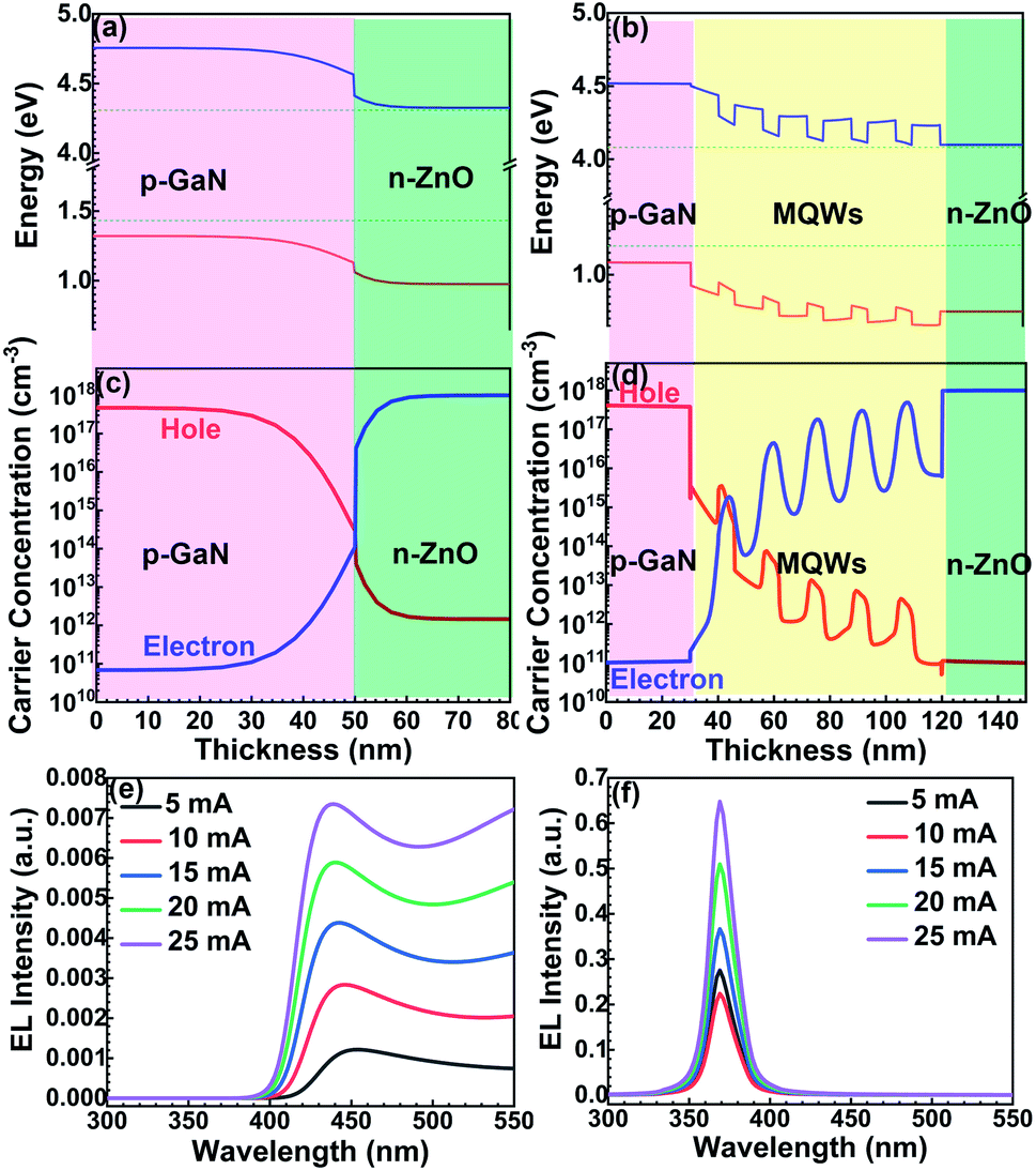 | ||
| Fig. 5 Calculated (a) conduction band energy diagram and (b) valence band energy diagram at 25 mA for the p-GaN/n-ZnO diode and p-GaN/MQWs/n-ZnO diode, respectively. Calculated carrier concentrations in (c) p-GaN/n-ZnO diode and (d) p-GaN/MQWs/n-ZnO diode. Simulated EL emissions from (e) p-GaN/n-ZnO diode and (f) p-GaN/MQWs/n-ZnO diode. | ||
Conclusions
In summary, we demonstrated the operation of a UV-light-emitting ZnO heterojunction diode by employing ZnO/Zn0.9Mg0.1O MQWs as an active layer. The properties of the MQWs and the performance of the diode were investigated. High-quality MQWs with a notable QCE, smooth surface and sharp interfaces have been obtained. The diode exhibited efficient UV emission around 370 nm at room temperature. The overflow of electrons to the poor-quality p-GaN layer has been restricted, and the carriers have been confined in high-quality MQWs. The device shows better monochromaticity and high efficiency. It is meaningful to the development of ZnO-based UV optoelectronic devices.Conflicts of interest
There are no conflicts to declare.Acknowledgements
This work was supported by National Natural Science Foundation of China (grant no. 51972283, grant no. 91833301) and the Key Research and Development Program of Zhejiang Province (2021C01030).Notes and references
- S. Nakamura, Science, 1998, 281, 956 CrossRef CAS PubMed.
- T. Nishida, N. Kobayashi and T. Ban, Appl. Phys. Lett., 2003, 82, 1 CrossRef CAS.
- D. Zhu, D. J. Wallis and C. J. Humphreys, Rep. Prog. Phys., 2013, 76, 106501 CrossRef CAS PubMed.
- D. M. Bagnall, Y. F. Chen, Z. Zhu, T. Yao, S. Koyama, M. Y. Shen and T. Goto, Appl. Phys. Lett., 1997, 70, 2230 CrossRef CAS.
- A. Tsukazaki, A. Ohtomo, T. Onuma, M. Ohtani, T. Makino, M. Sumiya, K. Ohtani, S. F. Chichibu, S. Fuke, Y. Segawa, H. Ohno, H. Koinuma and M. Kawasaki, Nat. Mater., 2005, 4, 42 CrossRef CAS.
- Ü. Özgür, Y. I. Alivov, C. Liu, A. Teke, M. A. Reshchikov, S. Doğan, V. Avrutin, S. J. Cho and H. Morkoç, J. Appl. Phys., 2005, 98, 041301 CrossRef.
- A. Ohtomo, M. Kawasaki, T. Koida, K. Masubuchi, H. Koinuma, Y. Sakurai, Y. Yoshida, T. Yasuda and Y. Segawa, Appl. Phys. Lett., 1998, 72, 2466 CrossRef CAS.
- N. B. Chen and C. H. Sui, Mater. Sci. Eng., B, 2006, 126, 16 CrossRef CAS.
- A. Ohtomo, K. Tamura, M. Kawasaki, T. Makino, Y. Segawa, Z. K. Tang, G. K. L. Wong, Y. Matsumoto and H. Koinuma, Appl. Phys. Lett., 2000, 77, 2204 CrossRef CAS.
- T. Makino, N. T. Tuan, H. D. Sun, C. H. Chia, Y. Segawa, M. Kawasaki, A. Ohtomo, K. Tamura, T. Suemoto, H. Akiyama, M. Baba, S. Saito, T. Tomita and H. Koinuma, Appl. Phys. Lett., 2001, 78, 1979 CrossRef CAS.
- T. Makino, K. Tamura, C. H. Chia, Y. Segawa, M. Kawasaki, A. Ohtomo and H. Koinuma, Appl. Phys. Lett., 2002, 81, 2355 CrossRef CAS.
- C. H. Chia, T. Makino, K. Tamura, Y. Segawa, M. Kawasaki, A. Ohtomo and H. Koinuma, Appl. Phys. Lett., 2003, 2003(82), 1848 CrossRef.
- T. Makino, K. Tamura, C. H. Chia, Y. Segawa, M. Kawasaki, A. Ohtomo and H. Koinuma, Phys. Rev. B: Condens. Matter Mater. Phys., 2002, 66, 233305 CrossRef.
- H. H. Zhang, X. H. Pan, P. Ding, J. Y. Huang, H. P. He, W. Chen, Y. Li, B. Lu, J. G. Lu and Z. Z. Ye, Opt. Commun., 2013, 301–302, 96 CrossRef CAS.
- S. C. Su, H. Zhu, L. X. Zhang, M. He, L. Z. Zhao, S. F. Yu, J. N. Wang and F. C. C. Ling, Appl. Phys. Lett., 2013, 103, 131104 CrossRef.
- J. H. Lim, C. K. Kang, K. K. Kim, I. K. Park, D. K. Hwang and S. J. Park, Adv. Mater., 2006, 18, 2720 CrossRef CAS.
- S. Chu, M. Olmedo, Z. Yang, J. Y. Kong and J. L. Liu, Appl. Phys. Lett., 2008, 93, 181106 CrossRef.
- H. S. Kim, F. Lugo, S. J. Pearton, D. P. Norton, Y. L. Wang and F. Ren, Appl. Phys. Lett., 2008, 92, 112108 CrossRef.
- Y. S. Choi, J. W. Kang, B. H. Kim and S. J. Park, Opt. Express, 2013, 21, 31560 CrossRef PubMed.
- X. M. Zhang, M. Y. Lu, Y. Zhang, L. J. Chen and Z. L. Wang, Adv. Mater., 2009, 21, 2767 CrossRef CAS.
- O. Lupan, T. Pauporté, T. Le Bahers, B. Viana and I. Ciofini, Adv. Funct. Mater., 2011, 21, 3564 CrossRef CAS.
- Z. G. Li, M. M. Jiang, Y. Z. Sun, Z. Z. Zhang, B. H. Li, H. F. Zhao, C. X. Shan and D. Z. Shen, Nanascale, 2018, 10, 18774 RSC.
- S. S. Chen, C. X. Xu, X. H. Pan, H. P. He, J. Y. Huang, B. Lu and Z. Z. Ye, J. Mater. Chem. C, 2019, 7, 6534 RSC.
- P. Ding, X. H. Pan, Z. Z. Ye, H. P. He, H. H. Zhang, W. Chen, C. Y. Zhu and J. Y. Huang, Appl. Phys. A, 2012, 112, 1051 CrossRef.
- Y. Segawa, H. D. Sun, T. Makino, M. Kawasaki and H. Koinuma, Phys. Status Solidi A, 2002, 192, 14 CrossRef CAS.
- H. D. Sun, T. Makino, N. T. Tuan, Y. Segawa, M. Kawasaki, A. Ohtomo, K. Tamura and H. Koinuma, Appl. Phys. Lett., 2001, 78, 2464 CrossRef CAS.
- H. Zhu, C. X. Shan, B. Yao, B. H. Li, J. Y. Zhang, Z. Z. Zhang, D. X. Zhao, D. Z. Shen, X. W. Fan, Y. M. Lu and Z. K. Tang, Adv. Mater., 2009, 21, 1613 CrossRef CAS.
- Y. I. Alivov, J. E. Van Nostrand, D. C. Look, M. V. Chukichev and B. M. Ataev, Appl. Phys. Lett., 2003, 83, 2943 CrossRef CAS.
- S. Jha, J. C. Qian, O. Kutsay, J. Kovac Jr, C. Y. Luan, J. A. Zapien, W. J. Zhang, S. T. Lee and I. Bello, Nanotechnology, 2011, 22, 245202 CrossRef PubMed.
- J. Jeong, J. E. Choi, Y. J. Kim, S. Hwang, S. K. Kim, J. K. Kim, H. Y. Jeong and Y. J. Hong, Appl. Phys. Lett., 2016, 109, 101103 CrossRef.
- K. H. Baik, H. Kim, J. Kim, S. Jung and S. Jang, Appl. Phys. Lett., 2013, 103, 091107 CrossRef.
- G. Y. Zhu, J. T. Li, Z. S. Tian, J. Dai, Y. Y. Wang, P. L. Li and C. X. Xu, Appl. Phys. Lett., 2015, 106, 021111 CrossRef.
- J. Jiang, Y. Zhang, C. Chi, Z. Shi, L. Yan, P. Li, B. Zhang and G. Du, Appl. Phys. Lett., 2016, 108, 063505 CrossRef.
Footnote |
| † Electronic supplementary information (ESI) available. See DOI: 10.1039/d1ra06685d |
| This journal is © The Royal Society of Chemistry 2021 |