DOI:
10.1039/D1RA06513K
(Paper)
RSC Adv., 2021,
11, 32973-32980
Study on a one-dimensional defective photonic crystal suitable for organic compound sensing applications
Received
29th August 2021
, Accepted 11th September 2021
First published on 7th October 2021
Abstract
Organic-compound-based sensors have important applications, such as applications in geothermal power stations, the shoe industry, the extraction of vegetable oil, azeotropic calibration and medical science. Herein, a 1D photonic crystal (PC) with a defect has been used to develop a photonic-technology-based organic compound sensor with optimum performance. The structure of the proposed organic compound sensor consists of a water cavity sandwiched between two symmetric sub-PCs, which are composed of alternate layers of SiO2 and ZnO. The proposed air/(SiO2/ZnO)5/cavity/(SiO2/ZnO)5/glass structure with the optimized structural parameters achieves a quality factor that varies between a minimum value of 4968.2 and a maximum value of 6418.5. The FOM and sensitivity values of the proposed sensing design are on the order of 102 and 103, respectively. The LOD value of the proposed sensor is on the order of 10−5, which is very low, as is always expected for chemical sensing designs. Thus, the simple design and excellent performance make our design highly efficient and suitable for sensing applications in the industrial and biomedical fields.
1. Introduction
Photonic crystals (PCs) are multilayer smart composite structures with unusual and intriguing optical properties, in which the refractive index modulates periodically in one, two and three orthogonal directions.1–7 They have tremendous ability to control the propagation of incident electromagnetic waves of different frequencies. PCs are characterized by their photonic band gaps (PBGs), which effectively attenuate the incident light of certain frequencies inside the PBG and allow others to pass through the photonic structure. The formation of the PBG is due to the existence of multiple Bragg scattering of incident electromagnetic waves at the interface separating two different media.8–12 The two scientists Yablonovitch and John introduced the pioneering works on PBG and photon localization, respectively.13,14 At present, PCs are one of the hot topics in the research fields of photonics, electromagnetic, biological and biomedical engineering.15–18 Breaking the periodicity of photonic structures by introducing a defect within the structure generates a resonant tunneling mode, also called the defect mode, inside the PBG of the structure.19–21 This defect mode allows the incident radiation of the resonant wavelength to pass through the structure, and is very sensitive in sensing any minute changes in the refractive index of the defect layer. The strong confinement of the electric field inside the defect layer underlies the minute sensing and detection mechanism.22,23 The existence of the defect mode inside the PBG enhances the novelty of such defective PCs in comparison to the conventional structures. 1D defective PCs are the most appropriate photonic structures, and are used in many diversified applications due their low cost and easier fabrication techniques compared to 2D and 3D defective PCs.24,25 All the above-mentioned properties of 1D defective PCs makes their structures suitable to be used as sensors capable of detecting minute refractive index changes in many fields, such as the biological, food industry, safety, security, environmental, chemical engineering, agricultural and cosmetic fields.26,27
Amongst the variety of sensors available on the market that are suitable for the different applications discussed above, biosensors must be immersed into the analyte, unlike photonic biosensors, in which the sensing process is initiated by infiltrating only the defect layer region with the analyte. Basically, photonic biosensing devices are used to detect the chemical or biological properties of the sample, which is also called the analyte, such as the level of glucose in urine, the concentration of creatinine in blood serum, and brain tissues such as oligodendroglioma cells and brain lesions.28,29 Typical photonic biosensors consist of five parts: the sample to be detected, which is called the analyte, is the first part. The second part is the bioreceptor, which is used for sensing the analyte. The third is the transducer, which produces a measurable signal from the information from the bioreceptor. An electronic circuit that is used to convert the measurable signals from the transducer into digital form is the fourth one. Finally, a combination of software and hardware, which is known as a reader, is required to display the biosensing results.28–30
Organic compounds (OCs) are one of the most important chemical agents and are extensively used in our day-to-day life, including in the food industry, the chemical industry, cosmetics, disease diagnosis, biotechnology, medical research, etc. Although their use in industry is convenient, their direct release into the environment may cause issues. It is a well-known fact that organic compounds are used in the majority of chemical industries and that their chemical waste may become an unwanted source of environmental pollution in gaseous form, as well as a major hazard to human health. Environmental pollution due to organic compounds has long-term adverse side effects, and may become a source of fatal diseases in the human body. Therefore, it is necessary to develop mechanisms by which organic compounds can be detected in a timely manner for the prevention of such fatal diseases. At present, a number of conventional technologies are available for the detection of organic compounds, such as solvatochromic fluorescence probes, the electronic nose, the quartz crystal microbalance (QCM), solvent-response materials and chromatography-mass spectrometry, which involve extensive device setup for the purpose and suffer from other technological disadvantages including complicated handling, great expense, and time-consuming operation. In addition to the above-mentioned technologies, photonic-crystal (PC)-based detection technology has attracted great attention due to its tremendous sensing and detecting capabilities.31
Motivated by the aforementioned excellent research works,21–31 in this paper, we propose a chemical sensor capable of sensing minute changes in the refractive indexes of samples of the organic compounds (OCs) pentane, n-hexane, n-heptane and n-octane using a conventional 1D photonic crystal with a defect. All these organic materials are colorless and transparent liquids with odors similar to gasoline. These materials were selected based on their extensive use in various industrial applications, such as their involvement in the manufacture of various chemicals and plastics and their use in low temperature thermometers, as solvents to extract vegetable oil from crops, and in the petroleum industry during the refining process. Additionally, these materials have been placed on lists of substances with special health hazards due to their classification by the Occupational Safety and Health Administration (OSHA), National Institute for Occupational Safety and Health (NIOSH), and American Conference of Governmental Industrial Hygienists (ACGIH). Exposure to OCs is a probable cause of health issues such as cancer hazards, reproductive hazards, and skin drying and cracking in the human body. OCs may also damage the nervous system. All the OCs selected in this study are flammable and produce poisonous gases in the environment during a fire. In view of the aforementioned facts, rapid and cost-effective sensing technology capable of sensing and detecting very minute quantities of these OCs must be developed to avoid cancer, respiratory issues, and other diseases related to the nervous system.32–34 The presently available gas chromatograph technology is very expensive, which limits its use for the detection of OCs.35–37 Sensors based on nano-cantilevers and carbon nanotubes possess high sensitivity and are also rapid due to their fast response time, but their results are unstable under real test conditions. To date, there are several optical sensing technologies that are presently used for OC detection, but sensing of OCs is still very challenging.37
On the other hand, the proposed design is capable of measuring the shift in the position of the defect mode in the PBG of the respective structure depending on the change in the refractive index of the various OC samples under investigation. Comparison between the observed data and the experimentally available standard data is used to detect the presence of OCs via their refractive index values.35–37 To the best of our knowledge, this is the first time that a 1D PC with a defect has been used for sensing OCs by changing the position of the defect mode inside the PBG depending on the changes in the refractive indices of various organic samples under investigation. The organization of the proposed work is as follows: Section 2 presents the design of the proposed structure. The theoretical formulation is discussed in Section 3. Results and discussion pertaining to the work are presented in Section 4.
2. Structural design of the sensor
The proposed biosensor is capable of detecting various organic compounds via their refractive indices and consists of a conventional 1D defective photonic crystal, as shown in Fig. 1. In the proposed design, a water cavity is created between two symmetric 1D sub-PCs (SiO2/ZnO)N, which consist of alternating layers of SiO2 and ZnO. The period of the two sub-PCs is also identical and is equal to 5. The systematic design of the proposed structure [air/(SiO2/ZnO)5/water cavity/(SiO2/ZnO)5/glass] is shown in Fig. 1. The thicknesses of the SiO2 and ZnO layers are d1 = 240 nm and d2 = 140 nm, respectively. The cavity region of thickness d3 = 840 nm is filled with water of refractive index n3 = 1.33.37,38 The entire structure was fabricated on a glass substrate of refractive index ns = 1.52. The refractive indices of the SiO2 and ZnO material layers were taken to be n1 = 1.45 and n2 = 2.003, respectively. This type of cavity-based photonic bio/chemical sensor can be easily fabricated by means of available thin film fabrication techniques, such as spin-coating and dip-coating approaches.39–41
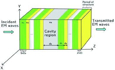 |
| | Fig. 1 Schematic design of the proposed chemical sensor composed of a 1D photonic crystal with a defect. | |
3. Theoretical formulation
The proposed simulations are based on the standard transfer matrix method (TTM),42–45 which is one of the best computational techniques for simulating 1D periodic multilayer structures. The total transfer matrix T, which connects the amplitude of the electric and magnetic fields at the incident and exit ends, is described as:| |
 | (1) |
Here T11, T12, T21 and T22 are elements of the total transfer matrix representing the whole structure. The t1, t2 and t3 represent the characteristic matrix of the first layer of SiO2, second layer of ZnO and the cavity layer, respectively.
The transmission coefficient of the whole structure [air/(SiO2/ZnO)N/cavity/(SiO2/ZnO)N/glass] can be obtained using the following expression:
| |
 | (2) |
where
s0 =
n0![[thin space (1/6-em)]](https://www.rsc.org/images/entities/char_2009.gif)
cos
ϒ0 and
ss =
nscos
ϒs represent the input and exit ends, respectively, for the transverse electric (TE) wave. For the transverse magnetic (TM) wave, these values would be
s0 = cos
ϒ0/
n0 and
ss = cos
ϒs/
ns.
ϒ0 indicates the incident angle from the air to the structure.
Finally, the transmittance of the whole structure can be defined as:
| |
 | (3) |
4. Results and discussion
In this section, we discuss the performance of our proposed organic compound sensor by studying the transmittance spectra at normal incidence. To simulate the transmittance of the proposed design [air/(SiO2/ZnO)N/cavity/(SiO2/ZnO)N/glass], the TMM has been used. The sensing performance of the organic compound sensor was evaluated via the figure of merit (FOM), quality factor (QF) and sensitivity values of the structure. Next, we studied the effect of the change in the refractive index of the organic compounds with respect to water and thickness of the cavity region on the performance of the proposed design.
4.1 Transmittance of the proposed design using a water cavity
For this purpose, using eqn (1) to (5), we calculated the transmittance of the electromagnetic waves (EMWs) passing through the structure at normal incidence. The numeric values of the controlling parameters of the design have already been discussed in Section 2 of this manuscript. Fig. 2 shows the transmittance of the proposed design [air/(SiO2/ZnO)N/cavity/(SiO2/ZnO)N/glass] as a function of the wavelength of the incident EMWs in blue with a water sample with a refractive index of 1.33 in the cavity region. Here, the period number N is equal to 5 and the incident angle is 0°. Fig. 2 shows a wide PBG with almost zero transmittance owing to the large refractive index contrast between the SiO2 and ZnO material layers of the structure. The existence of this PBG in the visible region of the electromagnetic spectrum is due to the destructive interference between the light rays transmitted from the various interfaces separating the different layers of the structure. Outside the PBG, a few ripples of high transmittance appear at either side of the PBG in the transmittance spectra. The cavity region is located in the middle of the design such that the two identical (SiO2/ZnO)N sub-PCs, which are located at either side of the cavity region, constitute identical Bragg mirrors. Hence, light can bounce back and forth into the cavity region between the two Bragg mirrors, leading to the confinement of EMWs, which is known as the localized defect mode inside the PBG. This localized defect mode inside the PBG can be delocalized within the PBG by infiltrating various organic compounds in place of water. The phenomena of the localization and delocalization of the defect mode within the PBG can also be understood using the Heisenberg uncertainty principle. Fig. 2 also shows a defect mode of 99% transmittance centered at a wavelength of 415.6 nm when the cavity region with a length of 840 nm is infiltrated with water of refractive index 1.33.
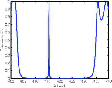 |
| | Fig. 2 Transmittance of the proposed design [air/(SiO2/ZnO)N/cavity/(SiO2/ZnO)N/glass] with a water cavity with a refractive index of 1.33 at normal incidence. The thickness of the cavity is 840 nm. | |
4.2 Effect of change in the refractive index of the cavity region on the performance of the sensor
Next, we infiltrated the cavity region with different organic compound samples one by one in place of water, as shown in Table 1. The transmittance spectra of the proposed sensor with various OCs are plotted Fig. 3. This figure shows that the defect modes associated with the OCs pentane, n-hexane, n-heptane and n-octane shifted to the higher wavelength side due to their higher refractive index. The normalized intensities of these defect modes also vary between 98% and 99%, which is relatively high. To evaluate whether the performance of the proposed sensor was capable of sensing minute refractive index changes due to changes in the OC samples infiltrated into the cavity region, we calculated the sensitivity (S), quality factor (QF) and figure of merit (FOM) of the proposed design under the influence of various OCs with respect to water.42–45
Table 1 Description of the various organic compound samples along with their refractive indices
| S. No. |
Organic material |
Refractive index |
| 1 |
Pentane |
1.35 |
| 2 |
n-Hexane |
1.37 |
| 3 |
n-Heptane |
1.38 |
| 4 |
n-Octane |
1.39 |
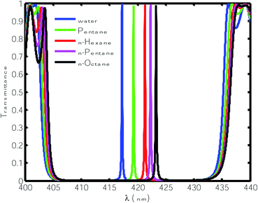 |
| | Fig. 3 Transmittance of the proposed design [air/(SiO2/ZnO)N/cavity/(SiO2/ZnO)N/glass] with different organic samples at normal incidence. The thickness of the cavity is 840 nm. | |
The QF of any efficient photonic sensor must be as high as possible. A high QF value ensures a narrower full width at half maximum (FWHM) of the resonant peak inside the PBG, which is essential and desirable for any excellent photonic sensor for use in chemical and biomedical sensing applications.
| |
 | (4) |
Here,
λd is the central wavelength of the resonant peak.
Next, we infiltrated the cavity region with each of the OC samples instead of water one by one; the refractive indices of the samples varied from 1.33 to 1.39. The change in the refractive index caused the localized defect mode to shift toward the higher wavelength side inside the PBG, as shown in Fig. 3. Under these conditions, the QF varied between 5271.3 and 6424.6. In order to achieve the highest sensing performance using the proposed sensor design, we then optimized the thickness of the cavity region to obtain a larger QF, narrower FWHM and optimum sensitivity values.
4.3 Effect of the thickness of the cavity region on the defect mode position with the water sample
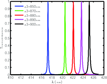
Here, we varied the thickness of the cavity region between 850 nm to 900 nm and studied the effect of this change on the position and FWHM of the resonant peaks inside the PBG when the cavity region was infiltrated with water only, as shown in Fig. 4. It can be observed from Fig. 4 that the increase in the thickness of the defect layer region caused the position of the defect mode to shift towards the higher wavelength side. Moreover, this increase in the thickness of the defect layer region increased the FWHM of the defect mode from 0.065 nm to 0.105 nm with changing thickness from 850 nm to 900 nm. Thus, incremental change in the thickness of defect layer affects the FWHM of the defect mode under investigation and lowers the quality factor value of the proposed chemical sensor from 6418.5 to 4049.5, hence compromising the performance. In addition, this change in the thickness of the defect layer region did not affect the normalized intensity, which remained fixed at 99%. All the above observations are tabulated in Table 2.
 |
| | Fig. 4 Transmittance of the proposed design [air/(SiO2/ZnO)N/cavity/(SiO2/ZnO)N/glass] with different cavity thicknesses at normal incidence. The cavity is loaded with water of refractive index 1.33. | |
Table 2 Details of the various defect modes at different defect layer thicknesses with water
| Thickness of defect layer |
Normalized intensity |
Defect peak wavelength |
FWHM |
Quality factor |
| 850 nm |
99% |
417.2 |
0.065 |
6418.5 |
| 870 nm |
99% |
420.5 |
0.075 |
5606.6 |
| 880 nm |
99% |
422.1 |
0.08 |
5276.3 |
| 890 nm |
99% |
423.7 |
0.1 |
4237 |
| 900 nm |
99% |
425.2 |
0.105 |
4049.5 |
4.4 Effect of the thickness of the defect layer on the position of the defect modes corresponding to the various organic compounds under investigation
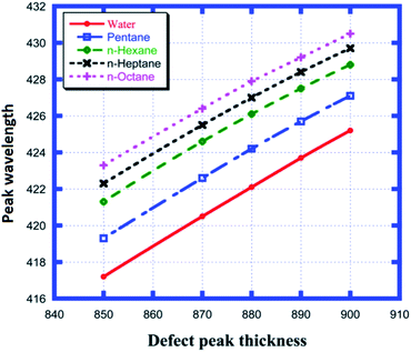
Fig. 5 shows the different defect mode positions inside the photonic band gap as a function of various cavity region thicknesses between 850 nm and 900 nm for each of the examined samples from water to n-octane, as shown in Table 3. Fig. 5 shows the linear dependence of the change in position of the defect mode due to the change in thickness of the cavity layer region for all four samples under investigation. All five straight line curves are satisfied by the equation λd = m × d3 + C. Here, λd and d3 are the position of the defect mode peak and thickness of the defect layer region, respectively. The slope m determines the rate of change of the position of the defect mode per unit change in the length of the defect layer region for a particular sample. This observation is one of the important findings that must be taken into account for the design of any photonic sensor. Thus, the higher the value of m, the greater the deviation in the position of the peak wavelength, which in turn increases the sensitivity of the structure. All the observations depicted in Fig. 5 are listed in Table 3.
 |
| | Fig. 5 Dependence of the peak wavelength on different cavity thicknesses for water, pentane, n-hexane, n-heptane and n-octane samples. | |
Table 3 Variation in the peak wavelength of the defect modes depending on the defect layer thickness when the cavity is loaded with different organic materials
| Material |
Defect peak wavelength for different thicknesses |
| 850 nm |
870 nm |
880 nm |
890 nm |
900 nm |
| Water |
417.2 |
420.5 |
422.1 |
423.7 |
425.2 |
| Pentane |
419.3 |
422.6 |
424.2 |
425.7 |
427.1 |
| n-Hexane |
421.3 |
424.6 |
426.1 |
427.5 |
428.8 |
| n-Heptane |
422.3 |
425.5 |
427 |
428.4 |
429.7 |
| n-Octane |
423.3 |
426.4 |
427.9 |
429.2 |
430.5 |
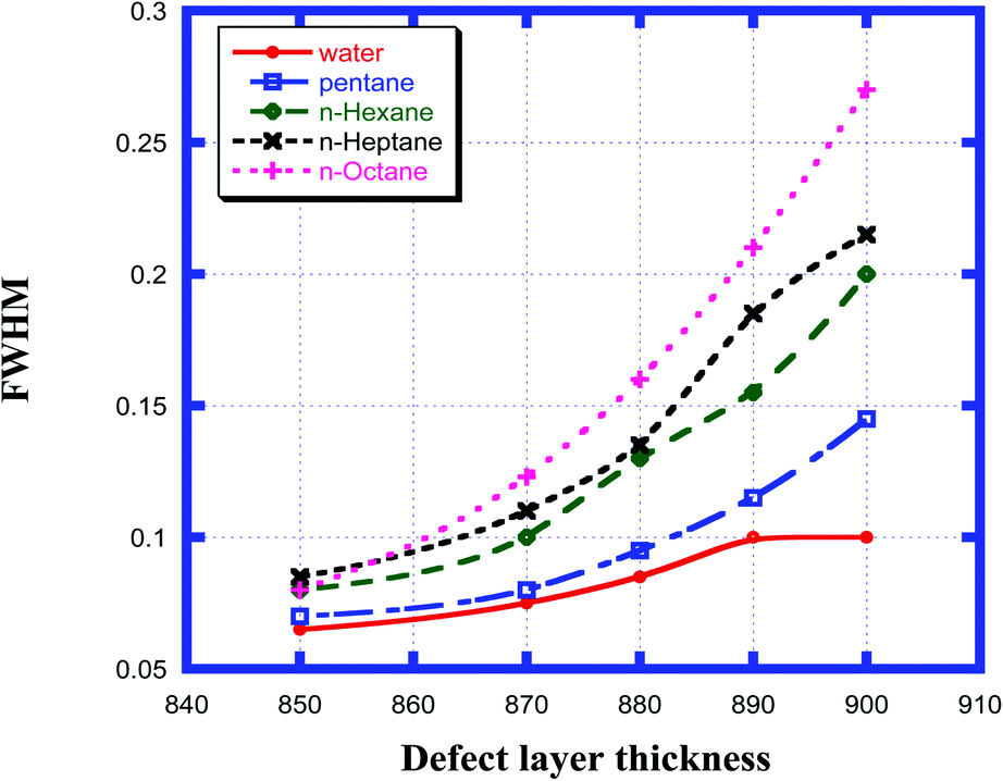
4.5 Effect of the change in the thickness of the defect layer region on the FWHM of the defect mode for the various organic compounds
The effect of the change in the thickness of the defect layer region of the proposed chemical sensor consisting of a 1D defective photonic crystal on the FWHM of the defect mode corresponding to each organic compound sample from pentane to n-octane with respect to water was studied. It was noted that as the thickness of the defect layer region changed from 850 nm to 900 nm, the FWHM of each sample increased and attained its maximum value when the defect layer thickness reached 900 nm. The FWHM of the defect mode for all samples from water to n-octane for defect layer thicknesses between 850 nm and 900 nm varied from a minimum value of 0.065 nm to a maximum value of 0.27 nm, as is evident in Fig. 6. All these observations are summarized in Table 4. From the data summarized in Table 4, we can conclude that the minimum FWHM value is obtained for all the organic samples under investigation at a defect layer thickness d3 = 850 nm. Obtaining the lowest FWHM value is an essential and desirable condition for obtaining high QF and FOM values. These high values are very crucial for designing an efficient chemical sensor.
 |
| | Fig. 6 Dependence of the FWHM of the resonant peak for different cavity thicknesses for water, pentane, n-hexane, n-heptane and n-octane samples. | |
Table 4 Table showing the FWHM of the different resonant peaks corresponding to the different defect layer thicknesses when the cavity is loaded with different organic materials
| Organic material |
FWHM for different defect layer thicknesses |
| 850 nm |
870 nm |
880 nm |
890 nm |
900 nm |
| Water |
0.065 |
0.075 |
0.085 |
0.1 |
0.1 |
| Pentane |
0.07 |
0.08 |
0.095 |
0.115 |
0.145 |
| n-Hexane |
0.08 |
0.1 |
0.13 |
0.155 |
0.2 |
| n-Heptane |
0.085 |
0.11 |
0.135 |
0.185 |
0.215 |
| n-Octane |
0.08 |
0.123 |
0.16 |
0.21 |
0.27 |
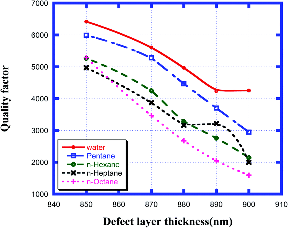
4.6 Effect of the change in the defect layer thickness on the quality factor value of the proposed chemical sensor
Fig. 7 shows how the quality factor of the proposed chemical sensor varied with the thickness of the defect layer region for the various organic compound samples from pentane to n-octane with respect to water. This figure shows that as the thickness of the cavity region increased from 850 nm to 900 nm, the quality factor values corresponding to samples from water to n-octane decreased from the maximum value at 850 nm and reached the minimum at a defect layer thickness of 900 nm. All the numeric observations from Fig. 7 are listed in Table 5 below. Thus, from the above data, we can conclude that to obtain the optimum value of QF, we must select a defect layer thickness of 850 nm.
 |
| | Fig. 7 Dependence of quality factor of the design for different cavity thicknesses for water, pentane, n-hexane, n-heptane and n-octane samples. | |
Table 5 Table showing the quality factor values of the different resonant peaks corresponding to different defect layer thicknesses when the cavity is loaded with different organic materials
| Organic material |
Quality factor for different defect layer thicknesses |
| 850 nm |
870 nm |
880 nm |
890 nm |
900 nm |
| Water |
6418.5 |
5606.6 |
4965.8 |
4237 |
4252 |
| Pentane |
5990 |
5282.5 |
4465.3 |
3701.7 |
2945.5 |
| n-Hexane |
5266.3 |
4246 |
3277.7 |
2758.1 |
2144 |
| n-Heptane |
4968.2 |
3868.2 |
3162.9 |
2315.7 |
1998.6 |
| n-Octane |
5291.3 |
3466.6 |
2674.4 |
2043.8 |
1594.4 |
4.7 Effect of the change in defect layer thickness on the sensitivity of the proposed chemical sensor
Finally, we examined the impact of variation of the defect layer thickness on the sensitivity of the proposed chemical sensor loaded with all four organic samples from pentane to n-octane with respect to water. The sensitivity (S) of any chemical sensor or biosensor is a very important parameter that aids in evaluating the performance of the sensor, and it is defined as:| |
 | (5) |
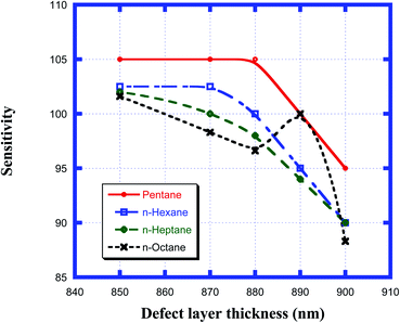
Here, Δλd is the change in the position of the defect mode inside the PBG due to the corresponding change in the refractive index of the sample to be sensed with respect to water. For this purpose, we have plotted the sensitivity of the proposed biosensor as a function of the thickness of the defect layer region for all the organic compounds from pentane to n-octane in Fig. 8. It has been observed that up to a defect layer thickness of 870 nm, there is either very minute change in the sensitivity of the proposed design, or it is constant for all organic samples except n-octane due to the large deviation of its refractive index of 1.39 with respect to that of water, which is 1.33. Further increase in the thickness of the defect layer beyond 870 nm causes a significant decrease in the sensitivity, which becomes more prominent when the thickness of the defect layer reaches 880 nm. The sensitivity of the design reaches its lowest value, which varies between 95 nm per RIU and 88.3 nm per RIU depending on the sample under investigation, at d3 = 900 nm. All the observations from Fig. 8 are listed in Table 6 below.
 |
| | Fig. 8 Dependence of the sensitivity of the design on different cavity thicknesses for pentane, n-hexane, n-heptane and n-octane samples. | |
Table 6 Table showing the sensitivity values of the design corresponding to different defect layer thicknesses when the cavity is loaded with different organic materials
| Organic material |
Sensitivity for different defect layer thicknesses |
| 850 |
870 |
880 |
890 |
900 |
| Pentane |
105 |
105 |
105 |
100 |
95 |
| n-Hexane |
102.5 |
102.5 |
100 |
95 |
90 |
| n-Heptane |
102 |
100 |
98 |
94 |
90 |
| n-Octane |
101.6 |
98.3 |
96.6 |
100 |
88.3 |
Furthermore, Table 7 below lists the performance of our chemical sensor in terms of the various parameters as defined in eqn (6) with a defect layer thickness of 840 nm to obtain the best results. This table shows that the quality factor of our sensing structures varies between a minimum value of 5.3 × 10³ with the sample n-octane to a maximum value of 6.4 × 10³ with water as the sensing medium. The sensitivity and FOM values of our sensor are almost 100 nm per RIU and 1.5 × 10³ per RIU respectively. In addition, the FWHM of the defect mode peak inside the PBG of the proposed design is also narrow for all samples under investigation, which is essential for obtaining higher sensitivity.
Table 7 Various parameters evaluating the performance of the proposed design with the optimum conditions
| Compound name |
Normalized intensity |
Defect peak wavelength (nm) |
FWHM (nm) |
Quality factor |
Sensitivity nm per RIU |
Figure of merit per RIU |
| Water |
99% |
415.6 |
0.075 |
5541.3 |
— |
— |
| Pentane |
99% |
417.6 |
0.065 |
6424.6 |
100 |
1538.5 |
| n-Hexane |
98% |
419.7 |
0.07 |
5995.7 |
102.3 |
1461.4 |
| n-Heptane |
98% |
420.6 |
0.07 |
6008.6 |
100 |
1428.6 |
| n-Octane |
98% |
421.7 |
0.08 |
5271.3 |
101.6 |
1270 |
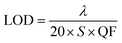
Finally, we calculated the limit of detection (LOD) of the proposed photonic structure. Basically, the LOD is used to correctly determine the concentration limits of the various organic compounds under investigation. The LOD can be evaluated using the defect mode wavelength (λ), S and QF of the proposed structure via the following relation:
| |
 | (6) |
The LOD values of the proposed structure loaded with pentane, n-hexane, n-heptane and n-octane as the analyte in the cavity region are 3.25 × 10⁻⁵ RIU, 3.42 × 10⁻⁵ RIU, 3.49 × 10⁻⁵ RIU and 3.93 × 10⁻⁵ RIU respectively. For the good performance of any chemical sensor, a low LOD value is always expected. Actually, the low LOD values indicate the smallest change in the refractive index that can be detected correctly. Thus, as required, our sensor has low LOD values on the order of 10−5.
5. Conclusions
In conclusion, it has been found that the localized defect mode inside the PBG of the 1D PBG structure with a defect can be utilized to design a chemical sensor that detects minute refractive index changes in the organic materials infiltrated into the cavity region. In this theoretical work, the transfer matrix method was used to study the transmission properties of the design air/(SiO2/ZnO)5/cavity/(SiO2/ZnO)5/glass. The results of this work show that the proposed design possesses high quality factor values that vary between 5.3 × 10³ per RIU and 6.4 × 10³ per RIU depending upon the refractive index of the pure organic sample. It has a sensitivity of approximately 100 nm per RIU and a large FOM value on the order of 103. Moreover, our design possesses low LOD values on the order of 10−5, which indicate the capability of the proposed design to resolve very minute changes in the refractive index of the analyte. In this work, we have also discussed the impact of changing the thickness of the cavity region on the most crucial parameters, namely, the FOM, QF and S, which determine the performance of any photonic sensor composed of a 1D PC with a defect. The proposed design may also be helpful for the investigation of bio-fluids, whose refractive indices vary between 1.33 and 1.40.
Conflicts of interest
The authors declare that there are no conflicts of interest.
Acknowledgements
This paper is supported financially by the Academy of Scientific Research and Technology (ASRT), Egypt, under initiatives of Science Up Faculty of Science (Grant No. 7859). ASRT is the 2nd affiliation of this research.
References
- J. D. Joannopoulos, S. G. Johnson, J. N. Winn and R. D. Meade, Photonic Crystals: Molding the Flow of Light, Princeton University Press, Princeton, USA, 2nd edn, 2008 Search PubMed.
- J. C. Knight, J. Broeng, T. A. Birks and P. S. J. Russell, Science, 1998, 282, 1476 CrossRef CAS PubMed.
- C. M. Bowden, J. P. Dowling and H. O. Everitt, J. Opt. Soc. Am. B, 1993, 10, 280 CrossRef.
- S. K. Awasthi, A. Mishra, U. Malaviya and S. P. Ojha, Solid State Commun., 2008, 146, 506 CrossRef CAS.
- S. K. Awasthi, Indian J. Phys., 2021 DOI:10.1007/s12648-020-01939-5.
- S. K. Awasthi, R. Panda and L. Shiveshwari, Phys. Plasmas, 2017, 24, 072111 CrossRef.
- A. H. Aly, S. K. Awasthi, A. M. Mohamed, W. Sabra, M. Mobarak, Z. S. Matar and A. S. Shalaby, IOP Conf. Ser.: Mater. Sci. Eng., 2021, 1171, 012012, DOI:10.1088/1757-899x/1171/1/012012.
- S. K. Awasthi, R. Panda and L. Shiveshwari, Phys. Plasmas, 2018, 25, 052103 CrossRef.
- S. Gandhi, S. K. Awasthi and A. H. Aly, RSC Adv., 2021, 11, 26655–26665 RSC.
- A. H. Aly and F. A. Sayed, Int. J. Mod. Phys. B, 2020, 34(10), 2050091 CrossRef CAS.
- M. A. Awad and A. H. Aly, Ceram. Int., 2019, 45(15), 19036–19043 CrossRef CAS.
- A. Mishra, S. K. Awasthi, P. Singh, U. Malaviya and S. P. Ojha, J. Mod. Opt., 2012, 59(7), 601 CrossRef.
- E. Yablonovitch, Phys. Rev. Lett., 1987, 58, 2059 CrossRef CAS PubMed.
- S. John, Phys. Rev. Lett., 1987, 58, 2486 CrossRef CAS PubMed.
- T. Sang, R. Wang, J. Li, J. Zhou and Y. Wang, Opt. Commun., 2018, 413, 255 CrossRef CAS.
- A. H. Aly and Z. A. Zaky, Ultra-sensitive photonic crystal cancer cells sensor with a high-quality factor, Cryogenics, 2019, 104, 102991 CrossRef CAS.
- P. Lu, L. Men, K. Sooley and Q. Chen, Appl. Phys. Lett., 2009, 94, 131110 CrossRef.
- J. Peng, et. al., Sens. Actuators, A, 2017, 263, 209 CrossRef CAS.
- D. Cardadora, D. Vega, D. Segura, T. Trifonov and A. Rodríguez, Photonics Nanostructures: Fundam. Appl., 2017, 25, 46 CrossRef.
- P. S. Nunes, N. A. Mortensen, J. P. Kutter and K. B. Mogensen, Sensors, 2010, 10, 2348 CrossRef CAS PubMed.
- A. H. Aly, H. A. Elsayed, A. A. Ameen and S. H. Mohamed, Int. J. Mod. Phys. B, 2017, 31(31), 1750239 CrossRef CAS.
- A. H. Aly, Z. A. Zaky, A. S. Shalaby, A. M. Ahmed and D. Vigneswaran, Physica Scripta, 2020, 95(3), 035510 CrossRef CAS.
- H. Mukundan, A. Anderson, W. K. Grace, K. Grace, N. Hartman and J. Martinez, et. al., Sensors, 2009, 9, 5783 CrossRef CAS PubMed.
- A. Pandey, A. Tripathi, S. Srivastava and S. Jit, J. Nanoelectron. Optoelectron., 2017, 12, 331 CrossRef CAS.
- J. s. Li, Opt. Laser Technol., 2014, 56, 263 CrossRef CAS.
- E. Kanazawa, et. al., Sens. Actuators, B, 2001, 77, 72 CrossRef CAS.
- Q. Zhang, P. Wang, J. Li and X. Gao, Biosens. Bioelectron., 2000, 15, 249 CrossRef CAS PubMed.
- A. H. Aly, D. Mohamed, M. A. Mohaseb, N. S. Abd El-Gawaad and Y. Trabelsi, RSC Adv., 2020, 10, 31765 RSC.
- W. M. Nouman, S. E.-S. Abd El-Ghany, S. M. Sallam, A.-F. B. Dawood and A. H. Aly, Opt. Quantum Electron., 2020, 52, 287 CrossRef CAS.
- Z. A. Zaky and A. H. Aly, Appl. Opt., 2021, 60(5), 1411 CrossRef PubMed.
- D. Kou, S. Zhang, J. L. Lutkenhaus, L. Wang, B. Tang and W. Ma, J. Mater. Chem. C, 2017, 1–8 Search PubMed.
- P. Wolkoff, Indoor Air, 1995, 5, 5–73 CrossRef.
- A. P. Jones, Atmos. Environ., 1999, 33, 4535–4564 CrossRef CAS.
- C. Yu and D. Crump, Build. Environ., 1998, 33, 357–374 CrossRef.
- P. Wilkinson, et. al., Lancet, 2009, 374, 1917–1929 CrossRef.
- M. Hassan, A. Joshi, S. Madhavan and M. Amonkar, Int. J. Obes., 2003, 27, 1227–1232 CrossRef CAS PubMed.
- J. Tao, et. al., Sci. Rep., 2017, 7, 41640 CrossRef CAS PubMed.
- K. Ueno, T. Imamura and K. L. Cheng, Handbook of Organic Analytical Reagents, second edition, 1992 Search PubMed.
- W. Sabra and A. H. Aly, Opt. Quantum Electron., 2021, 53, 416 CrossRef CAS.
- A. Biswas, et. al., Adv. Colloid Interface Sci., 2012, 170, 2–27 CrossRef CAS PubMed.
- H. Sen, et. al., RSC Adv., 2016, 6, 4505–4520 RSC.
- Y. Chen, P. Luo, H. Cao and Z. Zhao, Int. J. Mod. Phys. B, 2018, 32, 1850049 CrossRef CAS.
- S. Jena, R. B. Tokas, S. Thakur and D. V. Udupa, Phys. E, 2019, 114, 113627 CrossRef CAS.
- C.-J. Wu and Z.-H. Wang, Prog. Electromagn. Res., 2010, 103, 169 CrossRef.
- Z. A. Zaky, A. M. Ahmed, A. S. Shalaby and A. H. Aly, Sci. Rep., 2020, 10, 9736 CrossRef CAS PubMed.
|
| This journal is © The Royal Society of Chemistry 2021 |
Click here to see how this site uses Cookies. View our privacy policy here. 
 Open Access Article
 This Open Access Article is licensed under a Creative Commons Attribution-Non Commercial 3.0 Unported Licence
 *a,
S. K. Awasthib,
D. Mohameda,
Z. S. Matarc,
M. Al-Dossarid and
A. F. Amine
*a,
S. K. Awasthib,
D. Mohameda,
Z. S. Matarc,
M. Al-Dossarid and
A. F. Amine