
 Open Access Article
 This Open Access Article is licensed under a Creative Commons Attribution-Non Commercial 3.0 Unported Licence
Low temperature NO2 gas sensing with ZnO nanostructured by laser interference lithography
Sergio Sanchez-Martın ab,
S. M. Olaizolaab,
E. Castañoab,
G. G. Mandayoab and
I. Ayerdi*ab
ab,
S. M. Olaizolaab,
E. Castañoab,
G. G. Mandayoab and
I. Ayerdi*ab
aCEIT-Basque Research and Technology Alliance (BRTA), Manuel Lardizabal 15, 20018. Donostia/San Sebastián, Spain. E-mail: iayerdi@tecnun.es
bUniversidad de Navarra, Tecnun, Manuel Lardizabal 13, 20018 Donostia/San Sebastián, Spain
First published on 21st October 2021
Abstract
ZnO conductometric gas sensors have been widely studied due to their good sensitivity, cost-efficiency, long stability and simple fabrication. This work is focused on NO2 sensing, which is a toxic and irritating gas. The developed sensor consists of interdigitated electrodes covered by a ZnO sensing layer. ZnO has been grown by means of the aerosol assisted chemical vapor deposition technique and then nanostructured by laser interference lithography with a UV laser. The SEM and XRD results show vertically oriented growth of ZnO grains and a 2D periodic nanopatterning of the material with a period of 800 nm. Nanostructuring lowers the base resistance of the developed sensors and modifies the sensor response to NO2. Maximum sensitivity is obtained at 175 °C achieving a change of 600% in sensor resistance for 4 ppm NO2 versus a 400% change for the non-nanostructured material. However, the most relevant results have been obtained at temperatures below 125 °C. While the non-nanostructured material does not respond to NO2 at such low temperatures, nanostructured ZnO allows NO2 sensing even at room temperature. The room temperature sensing capability possibly derives from the increase of both the surface defects and the surface-to-volume ratio. The long stability and the gas sensing under humid conditions have also been tested, showing improvements of sensitivity for the nanostructured sensors.
1. Introduction
Nowadays, there is an increasing concern about air pollution and nitrogen dioxide, NO2, is one of the main contributing gases. It is a toxic gas, irritating and a precursor of nitrate particles. The latter have a harmful effect in the atmosphere by increasing the PM level, which disturbs the normal functioning of the respiratory system.1–3 For this reason, a gas sensor capable of detecting NO2 in real time is necessary.ZnO is a metal oxide semiconductor (MOS) that has been widely studied for conductometric gas sensors due to its non-toxicity, wide availability and low-cost. ZnO has also electrical properties that fit the requirements for chemoresistive sensors well.4–7 Among them, the most important are its wide bandgap, a high electron mobility and chemical stability.8,9 For these reasons ZnO has been used to improve diverse applications, such as photoelectric energy converters through the photovoltaic effect,10 photodetectors relying on in the piezo-phototronic effect11 and it can work as well in gas sensor devices.12
The working mechanism of the ZnO-based sensors is based on the crystalline structure and the grain connections by necks. These interconnected grains form gatherings that are connected with others by grain boundaries. On the grains' surface, due to the temperature assistance, the adsorbed oxygen molecules remove electrons from the conduction band and trap these electrons at the surface as ions; this produces a band bending. Consequently, an electron-depleted layer is formed; this region is known as a space charged layer. In the transducer phase, the donor or acceptor gaseous electrons are absorbed on the metal oxide surface and exchange electrons with the MOS. If the gas is acceptor-type, the electrons are extracted from the MOS decreasing its conductivity. On the other hand, if the gas is donor-type, the opposite occurs, and the conductivity increases. The mechanism of charge transfer between the MOS and absorbed gas dictate the conductivity of the material.13 Therefore, the overall process during gas detection involves oxidation processes of the MOS, absorption of chemical species and electronic transfer of conduction-band electrons to the surface and the other way around.14,15
Increasing sensitivity and reducing operating temperature are key issues in chemoresistive sensors. In the case of ZnO-based sensors of NO2, several approaches have been proposed in pursuit of this objective. Modifying the morphology and structure is one of the most followed methods, since the grain size and the porosity have a big impact on the formation of the depletion layer, thus on the sensing mechanism.16–18 Another way to reach the room temperature performance is through additives, which tune the bandgap and also the carrier concentration.19–21 Hybrid structures with 2D materials like graphene and phosphorene have also been used. These sensors take advantage of the large surface-to-volume ratio. So heterojunctions or 2D materials doped with ZnO are used to improve the NO2 sensing.22,23 Light activation of the charge carriers is also used to replace thermal activation. When ZnO is irradiated with light, the electrons in the valence band can be excited to the conduction band, which enhances the absorption of oxygen by the ZnO, in a similar way to thermal activation.24,25
Among all the different techniques used to improve the gas sensitivity of ZnO, morphology and structure modification have been proved one of the most effective. The surface microstructuration of ZnO leads to a bigger surface area and porosity, which contribute with a higher number of active sites for gas reaction.26 Besides, it provides surface defects that also have a positive effect in the number of oxygen absorption places. On the other hand, the vertical growth of the ZnO directly on the electrodes improves the gas sensing due to the high surface area and an efficient carrier transport channel.27
For this work, the AACVD deposition technique used allows the growth of vertical grains directly on the interdigital electrodes. In addition, the material has been further nanostructured by means of nanosecond Laser Interference Lithography (LIL). In this way, we combine two techniques that improve the sensing mechanism allowing the detection of NO2 at room temperature.
2. Materials and methods
The sensors have been fabricated on 10 × 20 mm2 polished alumina substrate, Fig. 1a. A heater is located on the reverse side of the substrate while the sensing element is on the front side. The Pt thin film of both the heater and the electrodes has been deposited by DC sputtering in an Edwards ESM 100 system. Lift-off technique has been used to pattern the heater and electrodes geometries. The heater is shown in Fig. 1b. The IDEs configuration is shown in Fig. 1c, and the dimensions of the electrodes are presented in Table 1. In a fourth step, ZnO has been deposited on the platinum IDEs by AACVD (Fig. 1d). For the AACVD process, the solution has been prepared dissolving 1 g of zinc chloride (ZnCl2) in 100 ml of ethanol. The atomizer Palas UGF 2000 generates the micrometer-size droplets assisted by a flow of N2 with a pressure of 4 bar. Acting N2 also as a carrier gas, the aerosol is transported to the reaction chamber. The aerosol enters through a tailored toroidal shower with an aerosol flow pressure of 2.5 bar. The ZnO is deposited at 375 °C using a rigid mask to pattern the material directly on the interdigitated electrodes. The sensor device is thermally stabilized in a quartz furnace at 700 °C during 4 h in synthetic air, Fig. 1e. The last step is the nanostructuration of ZnO layer by means of Laser Interference Lithography (LIL), Fig. 1f.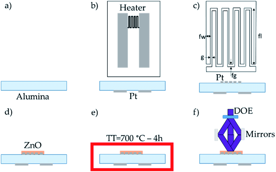 | ||
| Fig. 1 (a) Cross section of the alumina substrate. (b) Cross section and top view of the platinum deposited to perform as a heater. (c) Cross section and top view of interdigitated electrodes. (d) ZnO deposited on the interdigitated electrodes. (e) Thermal treatment (TT) of the ZnO deposited at 700 °C for 4 h. (f) ZnO structuration by LIL. | ||
| Gap between fingers, g | 20 μm |
| Gap at the end of the fingers, fg | 30 μm |
| Finger width, fw | 70 μm |
| Finger length, fl | 950 μm |
| Electrode thickness | 320 nm |
| Number of fingers, n | 11 |
| Total area | 1 mm2 |
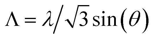
To perform the laser interference lithography an optical set-up is required. It has been designed and integrated with the reaction chamber. The first element of the optical set-up is the laser source. It has a wavelength of 355 nm, a pulse duration of 15 ns, a frequency of 500 Hz and a beam diameter of 3 mm. The laser beam is splitted by a diffractive optical element (DOE). This element is a diffractive beam splitter of 2 × 2 beams, i.e. it splits the input beam into 4 beams. The power per beam has been 200 mW. The full pattern angle is 40°, so that each beam is deflected 20° off the optical axis. To avoid aberrations, a three-beam interference is used instead of the four-beam technique. Three beams are collected by three mirrors that steer them to the interference spot. The period of the structures depends on the input angle of the laser beams into the interference plane as well as the laser wavelength.28
The ZnO samples after thermal treatment and LIL process have been analyzed in a FEG-SEM JSM-7000F, with an Integrated EDS Solution system. The crystallographic structure of ZnO thin films has been studied by X-ray diffraction (XRD) in a diffractometer Bruker D8 Advance A25, using an angle of incidence w = 2° and the characteristic wavelength of the Kα line for Cu (wavelength of 1.5406 Å). A JPK NanoWizard AFM has been employed to study the morphology of the ZnO. It has been operated in the intermittent contact mode using a silicon tip (r < 10 nm) with a resonant frequency of 300 kHz and a force constant of 40 Nm−1.
The response of the sensors have been measured in a cylindrical aluminium chamber of 10.8 ml. Bronkhorst mass flow controllers (MFC) have controlled the gas flow. The total flow into the chamber has been set at 120 sccm. The NO2 gas has been taken from certified bottles mixed with synthetic air (Air Liquide).
The sensor resistance is measured by applying a constant voltage of 3 V and measuring the current by means of a source-meter Keithley 2635A with automated data acquisition. Rg is the resistance after 30 minutes of exposure to gas, while Rs is the baseline resistance measured in air. The sensor is continuously heated to maintain the selected working temperature. Before the first measurement, it is stabilized overnight at a temperature of 225 °C.
3. Results and discussion
3.1 Material characterization
The material characterization has been performed through SEM images, AFM and XRD. The SEM images (Fig. 2) show the ZnO grains. The ZnO grows in a hexagonal wurtzite structure, with a good degree of preferential orientation along the c-axis. The thermal treatment of the material produces a rearrangement of atoms and also reduces the number of grain boundaries, having consequently a more stable and less resistive material.29–31 The ZnO thin film nanostructured by the laser interference is shown in Fig. 2c, where it can be seen the 2D periodic pattern achieved. The maximum intensity of the laser interference pattern produces the ablation of the material, while the minimum of the laser interference does not provide the substrate with enough temperature to undergo ablation. In Fig. 2d, the XRD pattern of the ZnO as grown confirms the formation of a hexagonal wurtzite structure according to the JCPDS, (36-1451). It exhibits a high intensity peak at (002) plane, corroborating the preferential crystallization along the c-axis. This result is confirmed by the ZnO grains perpendicular to the substrate surface observed in SEM images. Similar results have been achieved by other authors.32 | ||
| Fig. 2 SEM images of the ZnO deposition performed at (a) 375 °C, (b) 375 °C and a thermal treatment of 700 °C for 4 h and (c) 375 °C and a thermal treatment of 700 °C for 4 h and laser interference lithography. (d) XRD image of the ZnO grown at 375 °C (red curve). ZnO JCPDS (36-1451) data is at the bottom of the graphic for comparison. | ||
The AFM images present a deeper study of the morphology and structure of the ZnO grains. As it is shown in Fig. 3, the morphology and structure of the thin film varies with the thermal treatment and the posterior LIL process. The AFM image of the as-grown ZnO (Fig. 3a) shows a grain profile with a height variation of 200 nm, whereas, in the annealed ZnO layer the height is 40 nm approximately. This confirms the rearrangement of the atoms. The sample processed with laser shows a clear interference pattern. As it is observed in the Fig. 3c, the period of the pattern obtained is around 800 nm. It is in accordance with the theory of the three-beam interference, where the period is given by the formula:
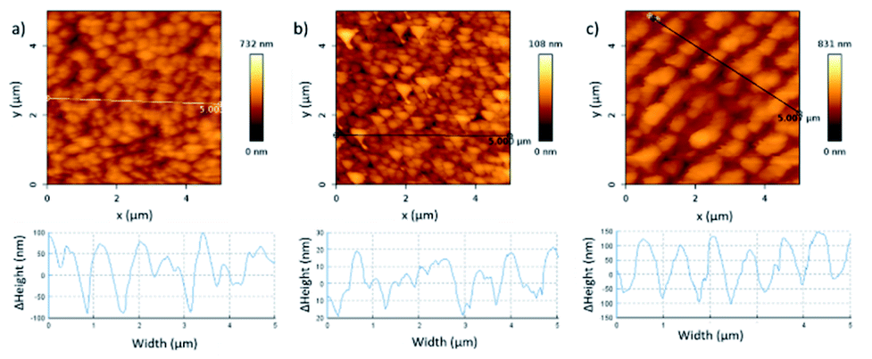 | ||
| Fig. 3 AFM images and the profile of the ZnO samples grown at (a) 375 °C, (b) 375 °C and a thermal treatment of 700 °C for 4 h and (c) 375 °C, a thermal treatment of 700 °C for 4 h and LIL. | ||
L. Parellada et al., have performed XPS measurements of the ZnO as grown, after thermal treatment and after laser interference exposure. They have reached the conclusion that both thermal and laser treatments through an increase of oxygen vacancies and/or interstitials regions the material gain Zn. Besides, the XPS results show a relationship between stoichiometry and stress of the material.36
3.2 Sensor response
In order to observe the influence of the laser nanostructuration on the ZnO gas sensing properties, tests have been performed in two type of sensors, firstly with the only-annealed ZnO, and secondly with the ZnO annealed and then processed by laser.The results obtained for both sensors in the temperature range from 125 to 200 °C are shown in Fig. 4. In the case of the thermal treated sensor, the relative resistance change increases with decreasing temperatures, so the sensitivity of the sensor increases. On the other hand, the laser processed sensor show a sensitivity peak at 175 °C and then it lessens for lower temperatures. As it is shown in Table 2, the recovery percentage of the baseline resistance decreases with the temperature in both sensors.
 | ||
| Fig. 4 Dynamic response curves of zinc oxide (only annealed and processed with laser interference) to decreasing NO2 concentrations (4, 2, 1 and 0.5 ppm) at 4 different temperatures (200 to 125 °C). | ||
| TT resistance recovery | TT + LIL resistance recovery | |||
|---|---|---|---|---|
| 15 min | 30 min | 15 min | 30 min | |
| 200 °C | 95% | 99% | 82% | 92% |
| 175 °C | 88% | 94% | 87% | 92% |
| 150 °C | 82% | 88% | 76% | 84% |
| 125 °C | 66% | 73% | 60% | 71% |
In addition, a difference that means an advantage in the ZnO as sensing material after laser processing can be noticed. The resistance value of the material decreases, which is always a desirable feature for an easier implementation of signal processing circuits, and for having a more power-efficient device. This can be due to an improvement in the conduction channels between the grains in the material as a result of the heat accumulation produced during the laser process that, as aforementioned, is comparable to a rapid thermal treatment.
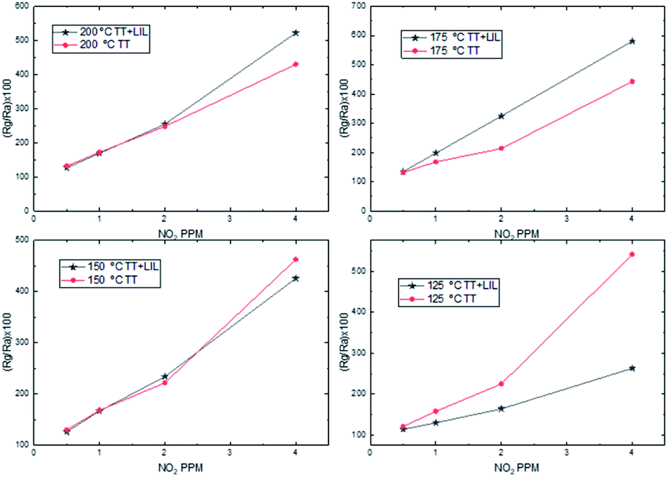
The following figure (Fig. 5) compares the response of samples with laser (labelled TT + LIL and plotted with stars) and without laser processing (plotted with circles) at four different temperatures.
 | ||
| Fig. 5 Sensitivity to nitrogen dioxide of the only-annealed samples compared to the annealed samples with LIL process at different temperatures. | ||
The sensitivity is higher at 200 °C and 175 °C in the sensors with LIL process. For the temperature of 150 °C, the sensitivity is similar in both sensors, and for the 125 °C case the sensitivity is better for the only annealed sensor. The highest increase is achieved at 175 °C, which shows an increase in the response from 400% to 600%. This magnitude is similar or higher than the obtained in other works in the literature with the sensor working in a temperature range between 125 °C and 175 °C.37–39
While non-processed samples do not respond to NO2 at temperatures below 100 °C, it has been possible to detect NO2 with the LIL processed samples down to 50 °C and even at room temperature, as Fig. 6 shows. While the recovery time (Table 3) gets longer as temperature decreases, it is remarkable that the device still has a perfectly measurable response even at room temperature, which can be seen in the sensitivity curves in Fig. 7.
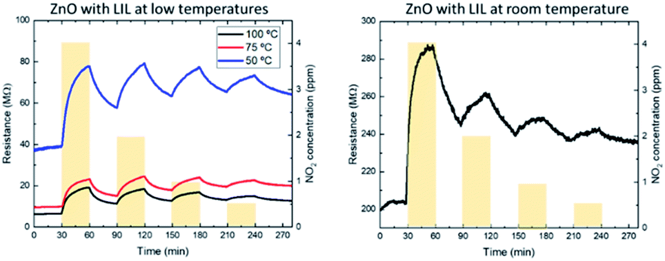 | ||
| Fig. 6 Dynamic response curves of zinc oxide (only annealed and processed with laser interference) to decreasing NO2 concentrations (0.5 to 4 ppm range) at 3 different temperatures (100, 75 and 50 °C) (left) and at room temperature (right). | ||
| TT + LIL resistance recovery | ||
|---|---|---|
| 15 min | 30 min | |
| 100 °C | 52% | 62% |
| 75 °C | 51% | 61% |
| 50 °C | 39% | 51% |
| RT | 35% | 47% |
 | ||
| Fig. 7 Sensitivity curves of zinc oxide processed by laser in the 0.5 to 4 ppm range at 3 different temperatures (100, 75 and 50 °C) (left) and at room temperature (right). | ||
The room temperature gas sensing with the laser-processed sensor in contrast to the unprocessed one, could be due to several factors. ZnO can contain point defects in the form of missing atoms, oxygen or zinc vacancies, interstitial ions of Zn or O, and substituted atoms, antisites of Zn or O. Oxygen vacancies have been proposed by several authors as the main contributor to ZnO gas sensitivity due to its low formation energy.40–42 However, the sensitivity improvement not only comes because of oxygen vacancies, but also because of the Zn interstitials.43 K. Ganapathi et al. show the effects of nanostructuring (flower-like nanostructures) the ZnO on the sensing of NO2. They proved that a superior sensor response is achieved due to the presence of oxygen vacancies and zinc interstitials. They also demonstrate that NO2 interacts with the ZnO in different ways. These have been verified by a XPS study of the ZnO after NO2 exposure through the formation of different nitrogen species, reduction in oxygen concentration and shift in Zn peak.44 Another work done by L. Parellada et al. shows that Laser Induced Periodic Surface Structures (LIPSS) can modify the morphology and defects of the ZnO. They analyse the ZnO by Raman spectroscopy, revealing a decrease of the ZnO wurtzite structure and an increase of the surface defects such as Zn interstitials.45 Regarding the analysis of both works, the results that have been obtained in this work could indicate that a higher number of surface defects are obtained by processing the material with laser interference.
On the other hand, vertically oriented ZnO nanomaterials have been proved beneficial for gas sensing. The ZnO growth along the c-axis provides high carrier mobility, which is essential for low ppm–ppb level sensing performance.46 As it is shown in Fig. 2a and d, the SEM and XRD display the growth of ZnO grains vertically oriented. Besides, the nanostructuration of the material increases the material surface area and therefore the surface-to-volume ratio, which has been proved relevant to perform room temperature NO2 gas sensing with ZnO.17,37,47 Therefore, the vertically oriented growth of the ZnO grains in addition to a rise of the surface-to-volume ratio improve the sensing performance of the sensor.
Regarding the summary of different nanostructured ZnO-based sensors of NO2 (Table 4), it is observable that the majority of them cannot work at room temperatures. Although, among them, there are devices capable of sensing at room temperature with a good sensitivity and stability.
The limit of detection (LOD) has been calculated for every sample at different work temperatures. It has been calculated through the following equation 3σ/a, where σ is the standard deviation of the linear regression and a is the slope.51 As Table 5 shows, the limit of detection is lower at higher temperatures and it decreases while the temperature decrease. It is also remarkable that the LOD is smaller for the sensors with the thermal and laser treatment, being minimum for the case of TT + LIL working at 175 °C.
| Sample | LOD (ppm) | Sample | LOD (ppm) |
|---|---|---|---|
| TT at 200 °C | 0.14 | TT + LIL at 200 °C | 0.17 |
| TT at 175 °C | 0.43 | TT + LIL at 175 °C | 0.09 |
| TT at 150 °C | 0.53 | TT + LIL at 150 °C | 0.24 |
| TT at 125 °C | 0.62 | TT + LIL at 125 °C | 0.32 |
| TT + LIL at 100 °C | 0.40 | ||
| TT + LIL at 75 °C | 0.48 | ||
| TT + LIL at 50 °C | 0.51 | ||
| TT + LIL at RT | 1.1 |
The long-term stability is a key factor for the gas sensing devices, to demonstrate the long durability of the gas sensor, two identical processes have been carried out. Both measurements have been performed at 200 °C, for 4 ppm, 2 ppm, 1 ppm and 0.5 ppm. The first one has been done with the sensor recently fabricated. The second measurement has been performed after two weeks, during these two weeks several measurements with humidity have been performed. The result shown in Fig. 8 prove that there is no substantial changes in the sensor behavior, only a resistance shift is present in the case of a concentration of 4 ppm.
 | ||
| Fig. 8 Dynamic response curves of zinc oxide (only annealed) to decreasing NO2 concentrations (4, 2, 1 and 0.5 ppm) at 200 °C for a new gas sensor and after two weeks. | ||
Physisorbed and chemisorbed water molecules form OH− ions that are attached to the ZnO for temperatures from 200 °C up to 400 °C. This leads to a reduction of the baseline resistance. Furthermore, the absorbance of water by the ZnO surface produces a decrease of the sensor response due to a less number of chemisorption oxygen spices. At high levels of humidity, the water molecules can act as well as barrier against NO2 absorption.52–54 In Fig. 9 and Fig. 10, the dynamic response of the gas sensor at 200 °C is shown. Resistance measurements have been performed for two different relative humidity 25% and 50% for two kind of sensor, one only annealed and other annealed and processed by LIL. The results show a resistance drop when the sensor is in contact with the water molecules in all cases, this is in concordance with the theory. Furthermore, the resistance baseline for the sensor processed by laser is lower than the only annealed and the stabilization when it is in contact with the water molecules is faster. Table 6 shows the sensitivity achieved for every configuration, showing an improvement of the sensor treated by laser, since the sensitivity does not vary from being in dry air or in humid conditions for a 25% of relative humidity. The sensor only annealed also show promising results under a 25% of relative humidity, varying only a 12.5% and a 4% for 1 ppm and 0.5 ppm concentrations respect to the sensor performance in dry air. When performing the experiments for a 50% of relative humidity, the sensor only annealed has a 20% and 4% variation for 1 ppm and 0.5 ppm. Whilst the patterned one has a 17% and 1.7% less sensitivity, presenting a soft improvement. Similar ZnO structures have been probed to improve the gas sensing in humid environment. R. L. Fomekong et al., have grown ZnO through spray pyrolysis, which is a similar technique than AACVD, performing measurements under different relative humidity up to 10%. Showing as well, a decrease in the baseline resistance and a reduction of the sensitivity for a 100 ppm concentration of NO2.55 S. Vallejos et al., performed gas sensor based on ZnO films with rod and needle morphology via AACVD. The sensing under dry or humidity ambient show the reduction of humidity interference due to a higher concentration of oxygen vacancies and higher surface-to-volume ratio of the structures, this information has been extracted from XPS and water CA analysis. These results can be extrapolated to explain the improvement achieved by the sensor processed by laser.56
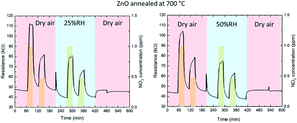 | ||
| Fig. 9 Dynamic response curves of zinc oxide (only annealed) to decreasing NO2 concentrations (1 and 0.5 ppm) at 200 °C with dry air and 25% or 50% of relative humidity conditions. | ||
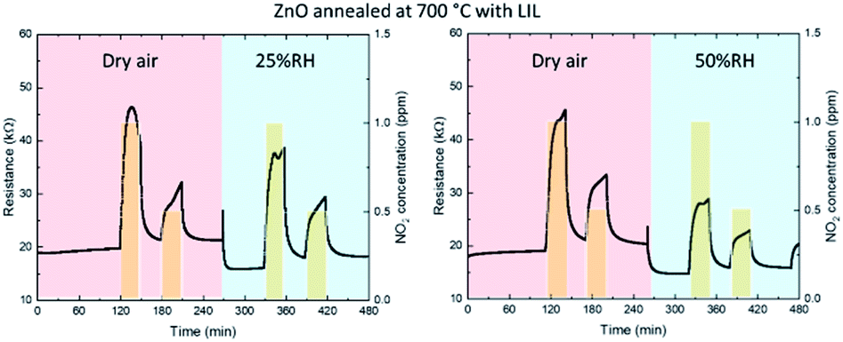 | ||
| Fig. 10 Dynamic response curves of zinc oxide (after annealing and LIL) to decreasing NO2 concentrations (1 and 0.5 ppm) at 200 °C with dry air and 25% or 50% of relative humidity conditions. | ||
| Sensitivity (sensor only annealed) | Sensitivity (sensor annealed and LIL) | |||||
|---|---|---|---|---|---|---|
| Dry air | 25% RH | 50% RH | Dry air | 25% RH | 50% RH | |
| 1 ppm | 240 | 210 | 193 | 255 | 251 | 212 |
| 0.5 ppm | 168 | 162 | 161 | 170 | 170 | 167 |
4. Conclusions
ZnO has been deposited by AACVD and nanostructured by LIL. AACVD allows the vertical growth of ZnO grains. The three-beam laser interference lithography produces a 2D periodic pattern in the ZnO layer with a period of 800 nm. The sensor fabrication with these techniques gathers a series of benefits that make it very competitive. It allows improving the usual performance of this type of sensors, achieving a 600% of sensitivity for a concentration of 4 ppm at 175 °C. The resistance of the laser-processed sensor is more stable. Besides, the resistance decreases, which make this device more power-efficient. NO2 sensing at room temperature has been achieved, obtaining a 130% of sensitivity for a concentration of 4 ppm. The general sensing improvement as well as the room temperature NO2 gas sensing could come from several aspects. The first one is the increase of number of surface defects obtained by processing the material with laser interference lithography. The second one is the vertically oriented ZnO grains that our AACVD technique provides. The last one is that the surface pattern generated by the laser process increases the surface to volume ratio.Long-term stability and improvement of the gas sensing under humid ambient have been probed for 25% and 50% of relative humidity, increasing the sensitivity a 10% and 4% for the 25% RH condition for the sensor nanostructured by laser.
This work presents very promising NO2 room temperature gas sensing results, but further work must be done in order to improve the recovery time of the sensor.
Author contributions
Visualization, S. S. M., I. A. and G. G. M.; formal analysis, S. S. M., I. A. and G. G. M.; investigation, S. S. M., G. G. M., I. A., E. C and S. M. O.; experimental, S. S. M.; writing—original draft preparation, S. S M.; writing—review and editing, I. A., G. G. M.; supervision, G. G. M., I. A., E. C and S. M. O.; project administration and funding acquisition, S. M. O. All authors have read and agreed to the published version of the manuscript.Conflicts of interest
There are no conflicts to declare.Acknowledgements
This research has been supported by EU H2020 program 767285 “Nanostencil”. We acknowledge the support of our Ceit colleagues to perform this work. This investigation has also been supported by U4IIOT-Microtechnologies, in the framework of the Industrial Internet of Things-IIOT4.0". Funded by the Basque Government under the Elkartek funding scheme, (Ref: KK-2019/00101).References
- K. Ito, G. D. Thurston and R. A. Silverman, J. Exposure Sci. Environ. Epidemiol., 2007, 17, S45–S60 CrossRef CAS PubMed.
- A. Faustini, R. Rapp and F. Forastiere, Eur. Respir. J., 2014, 44, 744–753 CrossRef CAS PubMed.
- X. Chen, Y. Shen, W. Zhang, J. Zhang, D. Wei, R. Lu, L. Zhu, H. Li and Y. Shen, Appl. Surf. Sci., 2018, 435, 1096–1104 CrossRef CAS.
- C. Xiao, T. Yang, M. Chuai, B. Xiao and M. Zhang, Phys. Chem. Chem. Phys., 2016, 18, 325–330 RSC.
- V. S. Bhati, M. Hojamberdiev and M. Kumar, Energy Rep., 2020, 6, 46–62 CrossRef.
- S. Vallejos, N. Pizúrová, J. Čechal, I. Gràcia and C. Cané, J. Visualized Exp., 2017, 2017, 1–5 Search PubMed.
- G. K. Mani and J. B. B. Rayappan, Mater. Sci. Eng. B: Solid-State Mater. Adv. Technol., 2015, 191, 41–50 CrossRef CAS.
- C. W. Bunn, Proc. Phys. Soc., 1935, 47, 835–842 CrossRef CAS.
- T. Minami, Semicond. Sci. Technol., 2008, 20, S35–S44 CrossRef.
- Y. Zhang, L. Yang, Y. Zhang, Z. Ding, M. Wu, Y. Zhou, C. Diao, H. Zheng, X. Wang and Z. L. Wang, ACS Nano, 2020, 14, 10723–10732 CrossRef CAS PubMed.
- W. Peng, Z. Pan, F. Li, Y. Cai and Y. He, Nano Energy, 2020, 78, 105268 CrossRef CAS.
- S. Agarwal, P. Rai, E. N. Gatell, E. Llobet, F. Güell, M. Kumar and K. Awasthi, Sens. Actuators, B, 2019, 292, 24–31 CrossRef CAS.
- M. Graf, A. Gurlo, N. Bârsan, U. Weimar and A. Hierlemann, J. Nanopart. Res., 2006, 8, 823–839 CrossRef CAS.
- A. Dey, Mater. Sci. Eng. B: Solid-State Mater. Adv. Technol., 2018, 229, 206–217 CrossRef CAS.
- G. Korotcenkov, Mater. Sci. Eng. B: Solid-State Mater. Adv. Technol., 2007, 139, 1–23 CrossRef CAS.
- Y. Xia, J. Wang, X. Li, D. Xie, D. Zhou, L. Xiang and S. Komarneni, Ceram. Int., 2016, 42, 15876–15880 CrossRef CAS.
- R. Chen, J. Wang and L. Xiang, Sens. Actuators, B, 2018, 270, 207–215 CrossRef CAS.
- Y. Xia, L. Zhou, J. Yang, P. Du, L. Xu and J. Wang, ACS Appl. Electron. Mater., 2020, 2, 580–589 CrossRef CAS.
- T. Tesfamichael, C. Cetin, C. Piloto, M. Arita and J. Bell, Appl. Surf. Sci., 2015, 357, 728–734 CrossRef CAS.
- R. K. Sonker, B. C. Yadav, A. Sharma, M. Tomar and V. Gupta, RSC Adv., 2016, 6, 56149–56158 RSC.
- S. Jain, N. Karmakar, A. Shah and N. G. Shimpi, Mater. Sci. Eng. B: Solid-State Mater. Adv. Technol., 2019, 247, 114381 CrossRef CAS.
- Z. Wang, T. Han, T. Fei, S. Liu and T. Zhang, ACS Appl. Mater. Interfaces, 2018, 10, 41773–41783 CrossRef CAS PubMed.
- X. Li, Y. Zhou, H. Tai, Y. Jiang and Z. Li, Mater. Lett., 2020, 262, 127148 CrossRef CAS.
- Y. Zhou, C. Gao and Y. Guo, J. Mater. Chem. A, 2018, 6, 10286–10296 RSC.
- Q. Zhang, G. Xie, M. Xu, Y. Su, H. Tai, H. Du and Y. Jiang, Sens. Actuators, B, 2018, 259, 269–281 CrossRef CAS.
- P. Srinivasan, M. Ezhilan, A. J. Kulandaisamy, K. J. Babu and J. B. B. Rayappan, J. Mater. Sci.: Mater. Electron., 2019, 30, 15825–15847 CrossRef CAS.
- J. Xuan, G. Zhao, M. Sun, F. Jia, X. Wang, T. Zhou, G. Yin and B. Liu, RSC Adv., 2020, 10, 39786–39807 RSC.
- E. Stankevičius, M. Gedvilas, B. Voisiat, M. Malinauskas and G. Račiukaitis, Lith. J. Phys., 2013, 53, 227–237 CrossRef.
- L. D. Sappia, M. R. Trujillo, I. Lorite, R. E. Madrid, M. Tirado, D. Comedi and P. Esquinazi, Mater. Sci. Eng. B: Solid-State Mater. Adv. Technol., 2015, 200, 124–131 CrossRef CAS.
- Y. Min, PhD in Electronic, Photonic, and Magnetic Materials in Massachusetts, Institute of Technology, 2003.
- S. Sanchez-Martin, S. M. Olaizola, E. Castaño, E. Urionabarrenetxea, G. G. Mandayo and I. Ayerdi, RSC Adv., 2021, 11, 18493–18499 RSC.
- S. Chen, M. McLachlan, A. Sapelkin and R. Binions, J. Mater. Chem. A, 2015, 3, 22311–22315 RSC.
- T. Shimogaki, T. Ofuji, N. Tetsuyama, K. Okazaki, M. Higashihata, D. Nakamura, H. Ikenoue, T. Asano and T. Okada, Oxide-based Materials and Devices IV, 2013, 8626 CAS.
- Y. M. Lee, H. W. Yang and C. M. Huang, J. Phys. D: Appl. Phys., 2012, 45, 225302 CrossRef.
- Y. C. Lee, S. Y. Hu, W. Water, K. K. Tiong, Z. C. Feng, Y. T. Chen, J. C. Huang, J. W. Lee, C. C. Huang, J. L. Shen and M. H. Cheng, J. Lumin., 2009, 129, 148–152 CrossRef CAS.
- L. Parellada-Monreal, I. Castro-Hurtado, M. Martínez-Calderón, A. Rodriguez, S. M. Olaizola, D. Gamarra, J. Lozano and G. G. Mandayo, Appl. Surf. Sci., 2018, 441, 331–340 CrossRef CAS.
- M. Chen, Z. Wang, D. Han, F. Gu and G. Guo, J. Phys. Chem. C, 2011, 115, 12763–12773 CrossRef CAS.
- V. P. Dinesh, A. Sukhananazerin and P. Biji, J. Alloys Compd., 2017, 712, 811–821 CrossRef CAS.
- M. Procek, A. Stolarczyk and T. Pustelny, Nanomaterials, 2017, 7, 312 CrossRef PubMed.
- Y. Xu, L. Zheng, C. Yang, W. Zheng, X. Liu and J. Zhang, ACS Appl. Mater. Interfaces, 2020, 12, 20704–20713 CrossRef CAS PubMed.
- P. Sundara Venkatesh, P. Dharmaraj, V. Purushothaman, V. Ramakrishnan and K. Jeganathan, Sens. Actuators, B, 2015, 212, 10–17 CrossRef CAS.
- M. Al-Hashem, S. Akbar and P. Morris, Sens. Actuators, B, 2019, 301, 126845 CrossRef CAS.
- N. Han, X. Wu, L. Chai, H. Liu and Y. Chen, Sens. Actuators, B, 2010, 150, 230–238 CrossRef CAS.
- S. Kailasa Ganapathi, M. Kaur, M. Shaheera, A. Pathak, S. C. Gadkari and A. K. Debnath, Sens. Actuators, B, 2021, 335, 129678 CrossRef.
- L. Parellada-Monreal, I. Castro-Hurtado, M. Martínez-Calderón, L. Presmanes and G. G. Mandayo, Appl. Surf. Sci., 2019, 476, 569–575 CrossRef CAS.
- R. Ahmad, S. M. Majhi, X. Zhang, T. M. Swager and K. N. Salama, Adv. Colloid Interface Sci., 2019, 270, 1–27 CrossRef CAS PubMed.
- C. T. Foo, N. U. Saidin and K. K. Ying, Mater. Today: Proc., 2019, 7, 661–667 CAS.
- D. Yan, M. Hu, S. Li, J. Liang, Y. Wu and S. Ma, Electrochim. Acta, 2014, 115, 297–305 CrossRef CAS.
- H. Van Han, N. D. Hoa, P. Van Tong, H. Nguyen and N. Van Hieu, Mater. Lett., 2013, 94, 41–43 CrossRef.
- D. Zappa, E. Comini and G. Sberveglieri, Nanotechnology, 2013, 24, 444008 CrossRef CAS PubMed.
- H. A. Molla, R. Bhowmick, A. Katarkar, K. Chaudhuri, S. Gangopadhyay and M. Ali, Anal. Methods, 2015, 7, 5149–5156 RSC.
- R. Kumar, O. Al-Dossary, G. Kumar and A. Umar, Nano-Micro Lett., 2015, 7, 97–120 CrossRef PubMed.
- Q. Qi, T. Zhang, X. Zheng, H. Fan, L. Liu, R. Wang and Y. Zeng, Sens. Actuators, B, 2008, 134, 36–42 CrossRef CAS.
- J. Gong, Q. Chen, M. R. Lian, N. C. Liu, R. G. Stevenson and F. Adami, Sens. Actuators, B, 2006, 114, 32–39 CrossRef CAS.
- R. L. Fomekong and B. Saruhan, Chemosensors, 2019, 7, 1–12 CrossRef.
- S. Vallejos, I. Gràcia, N. Pizúrová, E. Figueras, J. Čechal, J. Hubálek and C. Cané, Sens. Actuators, B, 2019, 301, 127054 CrossRef.
| This journal is © The Royal Society of Chemistry 2021 |