
 Open Access Article
 This Open Access Article is licensed under a Creative Commons Attribution-Non Commercial 3.0 Unported Licence
Correlation of grain orientations and the thickness of gradient MoS2 films†
Hui-Ping Chang a,
Mario Hofmannb,
Ya-Ping Hsiehc,
You-Sheng Chena and
Jauyn Grace Lin*a
a,
Mario Hofmannb,
Ya-Ping Hsiehc,
You-Sheng Chena and
Jauyn Grace Lin*a
aCenter for Condensed Matters Sciences and Center of Atomic Initiatives for New Materials, National Taiwan University, Taipei 10617, Taiwan. E-mail: jglin@ntu.edu.tw
bDepartment of Physics, National Taiwan University, Taipei 10617, Taiwan
cInstitute of Atomic and Molecular Science, Academia Sinica, Taipei 10617, Taiwan
First published on 22nd October 2021
Abstract
In this study, we synthesized gradient MoS2 films with a home-made suspended mask and characterized them by transmission electron microscopy (TEM) and Raman spectroscopy. The advantage of using gradient films is to simultaneously produce numerous samples under the same growth condition but with different thicknesses. The cross-sectional TEM images and their Fourier transform spectra revealed the thickness dependency of the grain orientations for synthetic MoS2 films. Combining the TEM results and the data of Raman A1g and E12g peaks, we found the correlation between the grain orientation and the A1g/E12g peak area ratio. We demonstrated the potential of using the non-polarized Raman Spectroscopy to characterize the grain structures of synthetic MoS2 films.
Introduction
Transition metal dichalcogenides (TMDs) have attracted considerable interest in the past decade because of their two-dimensional (2-D) characteristics and various unique properties. TMDs cover a wide range of materials, including semiconductors (MoS2 and WSe2), semimetals (PtSe2) and ferromagnets (VSe2).1–4 Among many, MoS2 is the most extensively investigated TMD in terms of device applications and material synthesis. It can be fabricated into various kinds of devices such as transistors,1 electroluminescence devices,5 photodetectors,6 gas sensors,7 hydrogen-evolution-reaction catalysts,8 memristors,9 and memtransistors.10 Various methods for the scalable synthesis of MoS2 films have been developed, including chemical vapor deposition (CVD),11,12 atomic layer deposition (ALD),13 molecular beam epitaxy (MBE),14 and magnetron sputtering.15 Precursors such as Mo, MoO2, MoO3, MoCl5, S, H2S, and (NH4)2MoS4 were successfully demonstrated for their capability of forming MoS2 from single layer to multi-layers.11–17 In contrast to the micro-sized monolayer flakes, the synthetic MoS2 film is typically nanocrystalline with grain sizes ranging from tens to hundreds of nanometers. Different grain orientations lead to different applications. Horizontally oriented (in-plane) grains are suitable for electronic devices, while vertically oriented (out-of-plane) grains are efficient for electrocatalysts.From the precision point of view, transmission electron microscopy (TEM) is effective to probe the MoS2 grain structures, providing an important guideline for material design.18–20 For example,18 TEM results showed that MoS2 has a vertical growth mode after sulfurizing the Mo precursor of 5 nm at 550 °C; but it became horizontally oriented after annealing at 800 °C for 8 h. Some TEM studies reported the effects of precursor thickness19 and sulfurization time20 on the orientations of MoS2 or the growth mechanism of monolayer MoS2 flakes. However, TEM characterization is a destructive and time-consuming method.
On the other hand, the optical Raman spectroscopy is a fast and non-destructive tool to characterize 2-D materials. The Raman spectrum of MoS2 contains two major peaks, E12g and A1g, which represent the in-plane shear vibration and out-of-plane breathing vibration of the molecules, respectively.21 Qualitatively, the frequency difference between E12g and A1g is related to the layer number of MoS2 crystals22 and the A1g/E12g intensity ratio is sensitive to the orientation of MoS2.18,19 Although the theoretical simulation showed that the predominant orientation of grains and the distribution of orientation angles can be evaluated from the A1g/E12g peak area ratio, it is hard to experimentally control or identify the angular distribution of grains (not just horizontal and vertical). The polarized Raman study23 reported that the A1g/E12g ratio increased by a factor of 2 in MoS2 with 75% of grains being vertically grown, in comparison with that of horizontally grown MoS2.23 However, the relationship between the A1g/E12g ratio and the angular distribution of grains has not been experimentally established yet. Since the information of grain orientation is extremely important to the film-device applications, we conducted a parallel study on the TEM images and Raman spectra of the gradient MoS2 films, with an attempt to find the correlation between the A1g/E12g ratio and the angular distribution of grains. The advantage of using gradient films is to simultaneously produce numerous samples with various thicknesses.
Results and discussion
We fabricated two pieces of gradient MoS2 films under the same conditions but with different patterns (Fig. 1a and b). The Mo precursor layers of MoS2 were produced by the gradient deposition method adopted in a previous study.24 The sulfurization processes are described in the Methods section. We measured Raman spectra on nineteen successive sites of one gradient MoS2 film with “cross” pattern (Fig. 1a) and took cross-sectional TEM images on five MoS2 samples cut out from another gradient film with “squared” pattern (Fig. 1b). The thickness of the Mo precursor (tMo) on the measured site was calculated by a process described in S1 and S2.† | ||
| Fig. 1 (a) MoS2 gradient film for Raman measurements. The nineteen measurement sites are on the “cross” of film within the area of the red frame. The positions of sites and the calculation of tMo and tMoS2 are described in Table S2-2.† (b) Five square samples were cut from the gradient MoS2 film (marked by red frame) for the experiments of FIB and TEM. The calculation of tMo was described in Table S2-1.† | ||
Ten out of nineteen Raman spectra after the baseline removal are shown in Fig. 2a–e, with two spectra as a pair to correspond the thickness of the TEM sample. All Raman spectra display two peaks around 380 and 405 cm−2, representing the E12g and A1g mode of MoS2, respectively.22 Cross-sectional TEM images of five MoS2 samples are shown in Fig. 2f–j. In Fig. 2f (for the sample of tMo = 0.88 nm), the TEM image did not show any trace of MoS2. However, the Raman spectra of tMo = 0.75 and 0.93 nm exhibit E12g and A1g peaks, suggesting the existence of MoS2 in the sample of tMo = 0.88 nm. The reason for MoS2 not being found in the TEM image is probably because the MoS2 film is too thin and destroyed during the sputtering of the Pt layer, which is the protective layer to prevent the damage of dual-beam FIB (focused ion beam). Except in Fig. 2f, MoS2 textures with various grain orientations are clearly seen. The corresponding thicknesses of four MoS2 samples (tMoS2) were determined from TEM image (Fig. 2g–j) and they have a polynomial relation with tMo, as shown in Fig. 2k. Note that the tMo values of five TEM samples (tMo = 0.88, 1.55, 2.21, 2.88, and 3.54 nm) fall between the tMo values of ten Raman samples (tMo = 0.75, 0.93, 1.46, 1.64, 2.17, 2.35, 2.71, 2.89, 3.42, and 3.60 nm).
 | ||
| Fig. 2 (a)–(e) Ten Raman spectra of MoS2 films with two spectra in one graph to correspond the thickness of TEM sample. (f)–(j) Cross-section TEM images of five MoS2 samples. In the TEM images, the black region is Pt films (left), the dark grey region is MoS2 (middle), and the light grey region is the amorphous SiO2 (right). (k) tMoS2 versus tMo for the TEM samples of (g)–(j). The paired numbers in each sample mark their X and Y positions. The origin is also shown as the boundary condition of the polynomial fitting. | ||
The magnified and aligned TEM images are displayed in Fig. 3a–d with their Fourier transform being shown in Fig. 3e–h, respectively. The pattern and distance of bright spots in Fig. 3e–h provide the information of grain orientations. Fig. 3e has a two-fold symmetry of a pair-spot, indicating two kinds of predominant orientations with a tilted angle smaller than 20° with respect to the substrate surface. Fig. 3f shows a two-fold symmetry of an arc structure, indicating multiple grains with different orientations confined within an angle smaller than 30°. Fig. 3g has eight major spots, indicating predominant four kinds of grains with different orientations covering from 0 to 90°. Fig. 3h shows a two-fold symmetry of a big spot, indicating the preferred orientations are within 20°. It is noted that the relative coordination of bright spots changes 90° from Fig. 3e–h due to the change in grain orientation from horizontal to vertical.
 | ||
| Fig. 3 (a)–(d) Magnified cross-section TEM images of four MoS2 films. (e)–(h) The corresponding Fourier transform of (a)–(d). | ||
Next, we analyze the nineteen Raman spectra after the baseline removal and Lorentzian fitting (described in S3†). The Raman shifts of E12g and A1g peaks, frequency difference between the two peaks, intensity, normalized intensity, peak widths, and peak area are plotted against tMoS2 in Fig. 4a–f respectively. The tMoS2 dependences of E12g and A1g Raman shift are similar but with opposite trends (see Fig. 4a). They both show a dramatic variation at small thickness (tMoS2 < 5.46 nm), and then reach a constant value. The Raman shift of (A1g − E12g) increases first with tMoS2 increasing, and then saturates around 26.5 cm−1 with tMoS2 ≥ 5.46 nm (see Fig. 4b). The above thickness dependencies of Raman shifts are very similar with that found in layer-number dependency of MoS2 single crystal.22 In Fig. 4c, the thickness dependencies of A1g and E12g intensity have a similar characteristic, having a decreasing trend but with some oscillations. This decreasing trend is attributed to the optical field enhancement of Si as found in the MoS2 single crystal.22 We normalized the Raman peak intensity of MoS2 with the intensity of Si (ISi), as shown in Fig. 4d. Compared with Fig. 4c, the oscillation behavior becomes more profound and the decreasing trend becomes less significant. The oscillation behavior can be attributed to the optical interference of excitation and the emitted light in association with the interfaces of MoS2/SiO2 and SiO2/Si.26 In Fig. 4e, the peak-width of A1g increases slightly, while that of E12g decreases about 27% with an increase in tMoS2, and the two widths become comparable for tMoS2 ≥ 9.95 nm (see Fig. 4e). The change in the E12g peak-width may be attributed to the variation of force constants associated with the structural change.22 We therefore plotted the peak areas of A1g and E12g to include the variation of peak-width, as shown in Fig. 4f. In addition, the peak area ratio of A1g over E12g is calculated to remove the effects of Si-substrate and interfacial interferences.
 | ||
| Fig. 4 The tMoS2-dependencies of (a) A1g and E12g Raman shifts, (b) (A1g − E12g) Raman shift, (c) intensity of A1g and E12g, (d) normalized intensity of A1g and E12g with the intensity of silicon, (e) peak width of A1g and E12g, and (f) peak area of A1g and E12g. | ||
The A1g/E12g area ratio against tMoS2 is shown in Fig. 5a. Based on the slope of curve, the data were classified into 4 regions: (I) a near constant low value of A1g/E12g ratio (∼1.87), (II) a rising trend, (III) without clear trends and (IV) a linear relationship. These four regions can be correlated with TEM patterns in Fig. 3e–h in terms of the grain orientation and the MoS2 thickness. Here, we defined the angle between the c-axis of grain and the substrate surface normal as θ. Region I is for tMoS2 of 2.4 nm < tMoS2 < 5.5 nm and with predominant horizontal grains of |θ| < 20°, as found from Fig. 3e. Region II is for 5.5 nm < tMoS2 < 12.9 nm and with predominant horizontal grains of |θ| < 30° (Fig. 3f). Region III is for 12.9 nm < tMoS2 < 22.6 nm with both horizontal and vertical grains (Fig. 3g). Region IV is for 22.6 < tMoS2 < 30.4 with predominant vertical grains of 70° < |θ| < 90° (Fig. 3h). Overall, the A1g/E12g area ratio enhances with the increase in the tilt angle of grain by a factor of 2.2 from the lowest value (1.70) to the highest value (3.73).
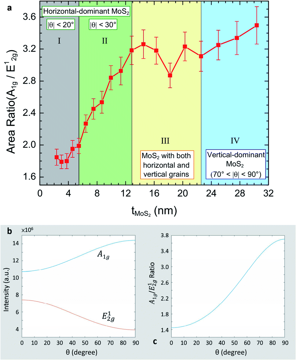 | ||
| Fig. 5 (a) The diagram of the A1g/E12g area ratio versus tMoS2 with four distinguishable regions, marked by different colors. The angular distribution shown in the insets are estimations based on TEM images and their corresponding Fourier transform. (b) Simulation of the intensity of A1g and E12g mode from θ = 0° to 90°. (c) Simulation of the ratio of A1g/E12g from θ = 0° to 90°. | ||
To theoretically explain the above-mentioned diagram, we adopted a method used in previous work23,25 to simulate the intensity of A1g and E12g, and the ratio of A1g/E12g by considering the contributions from the electric field of incident/scattered light, the numerical aperture of the objective lens (NA), and the Raman tensor matrices of A1g and E12g (eqn (1) and (2)).
The total scattering intensity (denoted as I in the following passages) of a vibrational mode can be calculated as shown below:
 | (1) |
![[E with combining right harpoon above (vector)]](https://www.rsc.org/images/entities/i_char_0045_20d1.gif) sc and in: vectors describing the electric field of the scattering laser and incident laser.
sc and in: vectors describing the electric field of the scattering laser and incident laser.
Cx, Cy, Cz: coefficients proportional to the integrated intensities of Ein,x, Ein,y and Ein,z.
A and B: coefficients related to NA.
Rij (i = x, y, z; j = x, y, z): the elements of Rxyz matrix.
 | (2) |
R1, R2 and R3 are the rotation matrix elements of the Euler angle (α, θ, γ) system (see S4† for details). (A, B) = (8.593, 5.111) for the numerical aperture of objective lens (NA) to be 0.9, and (Cx, Cy, Cz) = (13.722, 0.082, 2.192) for an X-polarized incident laser.23,25 In our simulation, we use (Cx, Cy, Cz) = (13.722 + 0.082, 13.722 + 0.082, 2 × 2.192) = (13.804, 13.804, 4.384) for the non-polarized laser beam, and considered α = 0 to 2π and γ = 0 to 2π for each value of θ.
Fig. 5b is the simulation of angle dependences of A1g and E12g intensity, showing that A1g increases and E12g decreases with θ increasing from 0° to 90°. The two simulation curves cannot be compared with the data in Fig. 4d because of the interference effect being dominant over the angular effect in the actual Raman scattering measurement. The interference effect can be removed by normalized the A1g intensity to the E12g intensity. Fig. 5c is the simulation of the angular-dependent A1g/E12g ratio, showing a monotonically enhancement from 1.447 (θ = 0°) to 3.697 (θ = 90°), which is a factor of 2.5. The simulation range is for the grain orientation varying from zero to 90° and the predicted enhancement factor of the A1g/E12g ratio is close to our experimental value (1.70 to 3.73 as shown in Fig. 5a). Therefore, it is evident that the enhancement of the A1g/E12g ratio with an increase in the MoS2 thickness originates from the increase of θ. However, the simulation curve in Fig. 5c does not completely match with the diagram of the A1g/E12g ratio versus thickness in Fig. 5a owing to the fact that the simulation is based on a simple model that all grains have the same size and with coherent angles from zero to 90°. In reality, our synthetic MoS2 films consisted of the grains with different sizes and specific angles. Therefore, further theoretical consideration and experiment design are urged to clarify the influences of different structural factors on the A1g/E12g ratio for 2-D materials.
Conclusions
In conclusion, we used the method of gradient synthesis to simultaneously produce numerous MoS2 film samples with different thicknesses and characterized them with TEM and non-polarized Raman spectroscopy. We demonstrated that it is possible to make MoS2 films of various thicknesses from 2 to 32 nm at the same time. The Fourier transform patterns of TEM images provide the information of grain orientation, which can be correlated with the parameters of the A1g/E12g peak area ratio extracted from non-polarized Raman spectra. We found a significant enhancement factor of the A1g/E12g ratio (2.2 by experiment; 2.55 by simulation) with a change of grain orientation by 90°, suggesting that the non-polarized Raman spectra can be an effective probe to determine the grain-orientations of synthetic multi-grained MoS2 films. The methodology in this study may be applicable to other TMD materials; thus, it benefits a fast development of large-scale production of TMD devices.Methods
Sample preparation
Molybdenum films were deposited by a typical e-beam evaporator on the Si/SiO2 (80 nm) substrate. The deposition rate is 0.1 Å s−1 measured by the thickness monitor. The details for the gradient deposition system and the sample thickness can be found in S1 and S2.†Si/SiO2/Mo was placed into the quartz tube equipped with a high temperature furnace. After vacuuming the tube to a pressure lower than 5 × 10⁻² torr, 1% H2S/Ar mixed gas flowed into the tube at a rate of 400 sccm till the pressure reached 3.6 torr. The heating process follows three steps: (i) from room temperature to 750 °C in 150 min (+4.8 °C min−1), (ii) at 750 °C for 60 min, and (iii) from 750 °C to room temperature in 150 min (−4.8 °C min−1). The flow rate of H2S/Ar mixed gas was kept the same during the whole heating process.
Raman measurements and analysis
Raman spectroscopy is equipped by a 532 nm laser and a computer controlled XYZ stage with the smallest step in X, Y direction being 1 μm. The numerical aperture of the objective is 0.9 and the size of the laser spot is around 6.25 μm2. Details for the site positions can be found in Table S2-2.† Details for the baseline removal and the fitting procedures can be found in S3.†FIB and TEM
A layer of 20 nm Pt was sputtered on the rectangular MoS2 film (Fig. 1b) as a protection layer, and then the substrate was cut and thinned by FIB (FEI Helios 600i) for cross-sectional TEM samples. The samples were characterized by the 300 kV TEM (FEI Tecnai G2 F30). Details about the thickness of MoS2 samples can be found in Table S2-1.†Author contributions
H.-P. Chang conducted the design of the gradient deposition system, sample synthesis, Raman measurement, simulation, data analysis and first draft writing. M. Hofmann proposed the idea of gradient deposition and provided the e-beam evaporator. Y.-P. Hsieh provided the raw materials, CVD system and Raman Spectroscopy. Y. S. Chen assisted the data analysis. J. G. Lin proposed the idea of combined characterization of TEM and Raman spectra, and provided the major research funding.Conflicts of interest
There are no conflicts to declare.Acknowledgements
J. G. Lin acknowledges the financial support from the Ministry of Science and Technology of Taiwan (ROC) under grants MOST 109-2112-M-002-006 and MOST 109-2123-M-002-002, and from National Taiwan University under NTU-109L900803. M. Hofmann and Y.-P. Hsieh acknowledge the financial support from the Ministry of Science and Technology of Taiwan (ROC) under grants of MOST 107-2112-M-002-004-MY3. The authors thank Ms. C.-Y. Chien and Mr H. R. Chen at National Taiwan University for the assistance of FIB and TEM experiment, respectively.References
- B. Radisavljevic, A. Radenovic, J. Brivio, V. Giacometti and A. Kis, Single-layer MoS2 transistors, Nat. Nanotechnol., 2011, 6, 147–150, DOI:10.1038/nnano.2010.279
.
- H. Fang, S. Chuang, T. C. Chang, K. Takei, T. Takahashi and A. Javey, High-Performance Single Layered WSe2 p-FETs with Chemically Doped Contacts, Nano Lett., 2012, 12, 3788–3792, DOI:10.1021/nl301702r
- Y. Wang, L. Li, W. Yao, S. Song, J. T. Sun, J. Pan, X. Ren, C. Li, E. Okunishi, Y. Q. Wang, E. Wang, Y. Shao, Y. Y. Zhang, H. T. Yang, E. F. Schwier, H. Iwasawa, K. Shimada, M. Taniguchi, Z. Cheng, S. Zhou, S. Du, S. J. Pennycook, S. T. Pantelides and H. J. Gao, Monolayer PtSe2, a New Semiconducting Transition-Metal-Dichalcogenide, Epitaxially Grown by Direct Selenization of Pt, Nano Lett., 2015, 15, 4013–4018, DOI:10.1021/acs.nanolett.5b00964
- M. Bonilla, S. Kolekar, Y. Ma, H. C. Diaz, V. Kalappattil, R. Das, T. Eggers, H. R. Gutierrez, M. H. Phan and M. Batzill, Strong room-temperature ferromagnetism in VSe2 monolayers on van der Waals substrates, Nat. Nanotechnol., 2018, 13, 289–293, DOI:10.1038/s41565-018-0063-9
- R. S. Sundaram, M. Engel, A. Lombardo, R. Krupke, A. C. Ferrari, P. Avouris and M. Steiner, Electroluminescence in Single Layer MoS2, Nano Lett., 2013, 13, 1416–1421, DOI:10.1021/nl400516a
- O. Lopez-Sanchez, D. Lembke, M. Kayci, A. Radenovic and A. Kis, Ultrasensitive photodetectors based on monolayer MoS2, Nat. Nanotechnol., 2013, 8, 497–501, DOI:10.1038/nnano.2013.100
- H. Li, Z. Yin, Q. He, H. Li, X. Huang, G. Lu, D. W. H. Fam, A. I. Y. Tok, Q. Zhang and H. Zhang, Fabrication of Single- and Multilayer MoS2 Film-Based Field-Effect Transistors for Sensing NO at Room Temperature, Small, 2011, 8, 63–67, DOI:10.1002/smll.201101016
- M. A. Lukowski, A. S. Daniel, F. Meng, A. Forticaux, L. Li and S. Jin, Enhanced Hydrogen Evolution Catalysis from Chemically Exfoliated Metallic MoS2 Nanosheets, J. Am. Chem. Soc., 2013, 135, 10274–10277, DOI:10.1021/ja404523s
- V. K. Sangwan, D. Jariwala, I. S. Kim, K. S. Chen, T. J. Marks, L. J. Lauhon and M. C. Hersam, Gate-tunable memristive phenomena mediated by grain boundaries in single-layer MoS2, Nat. Nanotechnol., 2015, 10, 403–406, DOI:10.1038/nnano.2015.56
- V. K. Sangwan, H. S. Lee, H. Bergeron, I. Balla, M. E. Beck, K. S. Chen and M. C. Hersam, Multi-terminal memtransistors from polycrystalline monolayer molybdenum disulfide, Nature, 2018, 554, 500–504, DOI:10.1038/nature25747
- Y. Zhan, Z. Liu, S. Najmaei, P. M. Ajayan and J. Lou, Large-Area Vapor-Phase Growth and Characterization of MoS2 Atomic Layers on a SiO2 Substrate, Small, 2012, 8, 966–971, DOI:10.1002/smll.201102654
- Y. H. Lee, X. Q. Zhang, W. Zhang, M. T. Chang, C. T. Lin, K. D. Chang, Y. C. Yu, J. T. W. Wang, C. S. Chang, L. J. Li and T. W. Lin, Synthesis of Large-Area MoS2 Atomic Layers with Chemical Vapor Deposition, Adv. Mater., 2012, 24, 2320–2325, DOI:10.1002/adma.201104798
- L. K. Tan, B. Liu, J. H. Teng, S. Guo, H. Y. Low and K. P. Loh, Atomic layer deposition of a MoS2 film, Nanoscale, 2014, 6, 10584–10588, 10.1039/c4nr02451f
- D. Fu, X. Zhao, Y. Y. Zhang, L. Li, H. Xu, A. R. Jang, S. I. Yoon, P. Song, S. M. Poh, T. Ren, Z. Ding, W. Fu, T. J. Shin, H. S. Shin, S. T. Pantelides, W. Zhou and K. P. Loh, Molecular Beam Epitaxy of Highly Crystalline Monolayer Molybdenum Disulfide on Hexagonal Boron Nitride, J. Am. Chem. Soc., 2017, 139, 9392–9400, DOI:10.1021/jacs.7b05131
- J. Tao, J. Chai, X. Lu, L. M. Wong, T. I. Wong, J. Pan, Q. Xiong, D. Chi and S. Wang, Growth of wafer-scale MoS2 monolayer by magnetron sputtering, Nanoscale, 2015, 7, 2497–2503, 10.1039/c4nr06411a
- X. Wang, H. Feng, Y. Wu and L. Jiao, Controlled Synthesis of Highly Crystalline MoS2 Flakes by Chemical Vapor Deposition, J. Am. Chem. Soc., 2013, 135, 5304–5307, DOI:10.1021/ja4013485
- K. K. Liu, W. Zhang, Y. H. Lee, Y. C. Lin, M. T. Chang, C. Y. Su, C. S. Chang, H. Li, Y. Shi, H. Zhang, C. S. Lai and L. J. Li, Growth of Large-Area and Highly Crystalline MoS2 Thin Layers on Insulating Substrates, Nano Lett., 2012, 12, 1538–1544, DOI:10.1021/nl2043612
- D. Kong, H. Wang, J. J. Cha, M. Pasta, K. J. Koski, J. Yao and Y. Cui, Synthesis of MoS2 and MoSe2 Films with Vertically Aligned Layers, Nano Lett., 2013, 13, 1341–1347, DOI:10.1021/nl400258t
- Y. Jung, J. Shen, Y. Liu, J. M. Woods, Y. Sun and J. J. Cha, Metal Seed Layer Thickness-Induced Transition From Vertical to Horizontal Growth of MoS2 and WS2, Nano Lett., 2014, 14, 6842–6849, DOI:10.1021/nl502570f
- L. Fei, S. Lei, W. B. Zhang, W. Lu, Z. Lin, C. H. Lam, Y. Chai and Y. Wang, Direct TEM observations of growth mechanisms of two-dimensional MoS2 flakes, Nat. Commun., 2016, 7(12206), 1–4, DOI:10.1038/ncomms12206
- Y. Zhao, X. Luo, H. Li, J. Zhang, P. T. Araujo, C. K. Gan, J. Wu, H. Zhang, S. Y. Quek, M. S. Dresselhaus and Q. Xiong, Interlayer Breathing and Shear Modes in Few-Trilayer MoS2 and WSe2, Nano Lett., 2013, 13, 1007–1015, DOI:10.1021/nl304169w
- C. Lee, H. Yan, L. E. Brus, T. F. Heinz, J. Hone and S. Ryu, Anomalous Lattice Vibrations of Single- and Few-Layer MoS2, ACS Nano, 2010, 4(5), 2695–2700, DOI:10.1021/nn1003937
- V. Vandalon, A. Sharma, A. Perrotta, B. Schrode, M. A. Verheijen and A. A. Bol, Polarized Raman spectroscopy to elucidate the texture of synthesized MoS2, Nanoscale, 2019, 11, 22860–22870, 10.1039/c9nr08750h
- Y. Nguyen, H.-P. Chang, M.-S. Hsieh, I. D. Santos, S.-D. Chen, Y.-P. Hsieh and M. Hofmann, Characterizing carrier transport in nanostructured materials by force-resolved microprobing, Sci. Rep., 2020, 10, 14177, DOI:10.1038/s41598-020-71147-y
- G. Turrell, Analysis of polarization measurements in Raman microspectroscopy, J. Raman Spectrosc., 1984, 15, 103–108, DOI:10.1002/jrs.1250150207
- H. Zhang, Y. Wan, Y. Ma, W. Wang, Y. Wang and L. Dai, Interference effect on optical signals of monolayer MoS2, Appl. Phys. Lett., 2015, 107, 101904, DOI:10.1063/1.4930257
Footnote |
| † Electronic supplementary information (ESI) available: S1: design of the gradient deposition, S2: tMo and tMoS2 calculation, S3: analysis procedures of Raman spectroscopy, and S4: theoretical simulation of the intensity versus θ (PDF). See DOI: 10.1039/d1ra05982c |
| This journal is © The Royal Society of Chemistry 2021 |