
 Open Access Article
 This Open Access Article is licensed under a
 Creative Commons Attribution 3.0 Unported Licence
Novel electrical properties and applications in kaleidoscopic graphene nanoribbons
Wenjing Bo,
Yi Zou* and
Jingang Wang *
*
College of Science, Liaoning Petrochemical University, Fushun 113001, China. E-mail: jingang_wang@lnpu.edu.cn; happylele1989@126.com
First published on 15th October 2021
Abstract
As one of the representatives of nano-graphene materials, graphene nanoribbons (GNRs) have more novel electrical properties, highly adjustable electronic properties, and optoelectronic properties than graphene due to their diverse geometric structures and atomic precision configurations. The electrical properties and band gaps of GNRs depend on their width, length, boundary configuration and other elemental doping, etc. With the improvement of the preparation technology and level of GNRs with atomic precision, increasing number of GNRs with different configurations are being prepared. They all show novel electrical properties and high tunability, which provides a broad prospect for the application of GNRs in the field of microelectronics. Here, we summarize the latest GNR-based achievements in recent years and summarize the latest electrical properties and potential applications of GNRs.
1 Introduce of GNRs
Since graphene nanomaterials were prepared in 2004, ribbon-shaped graphene nanomaterials have been studied. Studies have shown that GNRs are mainly sheared from two-dimensional graphene or carbon nanotubes. According to different boundary configurations, they are divided into the zigzag boundary (z-GNRs) and armchair boundary (a-GNRs). Based on the size effect of nanomaterials, GNRs with different boundary configurations show very different physical and chemical properties. Since GNRs are cut through graphene, the carbon atoms at the edges of GNRs are in an unsaturated state. This active edge state has become a very important factor in determining the edge structure. For a-GNRs, the two-dimensional planar structure of graphene is basically maintained, but for z-GNRs, the edge structure will be reconstructed at higher temperatures. In recent years, a variety of new two-dimensional semiconductor materials have shown good light responsiveness. Some nanosheets can be used as building blocks for various optoelectronic devices. These provide new research ideas in the field of future quantum communications, optoelectronic applications and other photodetectors.1–31.1 The lattice structures of GNRs
When discussing the characteristics of microscopic materials such as GNRs, many tools are used: such as Raman spectroscopy, scanning electron microscopy and transmission electron microscopy. When GNRs have different shapes, their Raman activity is different. In Raman spectroscopy, the chemical bonds, functional groups, number of layers, doping, defects and edge conditions of GNRs can be identified, and basic problems such as electrochemical interface structure, adsorption and reaction can be studied in depth. Electron microscopy techniques are also crucial, such as scanning electron microscopy (SEM) and transmission electron microscopy (TEM). SEM is used to depict the surface molecular structure at the nanometer level. Sometimes when facing ultra-thin characteristic materials that are easily scattered by electrons or absorbed by objects, the penetrating power is low, so TEM is used for observation. These advantageous tools provide great help to control the accuracy of GNRs.4–7GNRs obtained by etching graphene can exhibit arbitrary shapes. Although the etching method is simple to perform, the edge structure is not clear enough and cannot be prepared on a large scale. Therefore, the bottom-up method of preparing GNRs came into being. In recent years, surface synthesis technology has developed rapidly. It can precisely control the edge structure of GNRs prepared with atomic-level precision and can produce GNRs on a large scale by chemical vapor deposition. Due to the high activity and instability of the edge structure of the nanoribbons, the length of the synthesized GNRs is limited. But the nanobelt synthesized in solution overcomes this shortcoming. At present, the longest GNRs are obtained using in-solution synthesis methods. With theoretical calculations and experimental studies, studying new physical properties and applications of GNRs are becoming research hotspots.8–37
According to the direction shown, z-GNRs and a-GNRs can be cut out (Fig. 1(a)).38 7-a-GNRs with a single edge extension (structure highlighted by the dashed rectangle) (Fig. 1(b)).39 Sun's research team synthesized staggered narrow N = 8 a-GNRs (sn-8-a-GNRs) through a bottom-up approach, with alternating “bite” defects on the other side (Fig. 1(c)).40 Two 7-a-GNRs are fused to form 14-a-GNRs quantum dots by cross-dihydrogen coupling lateral edge fusion. Its image can be seen under non-contact atomic force microscopy (NC-AFM) (Fig. 1(d)).41 Researchers have synthesized GNRs (black), a two-dimensional form of carbon. GNRs have narrow parts (white) and wide parts (blue) alternating with each other. The photomicrograph shows one end of the nanoribbon (Fig. 1(e)).42
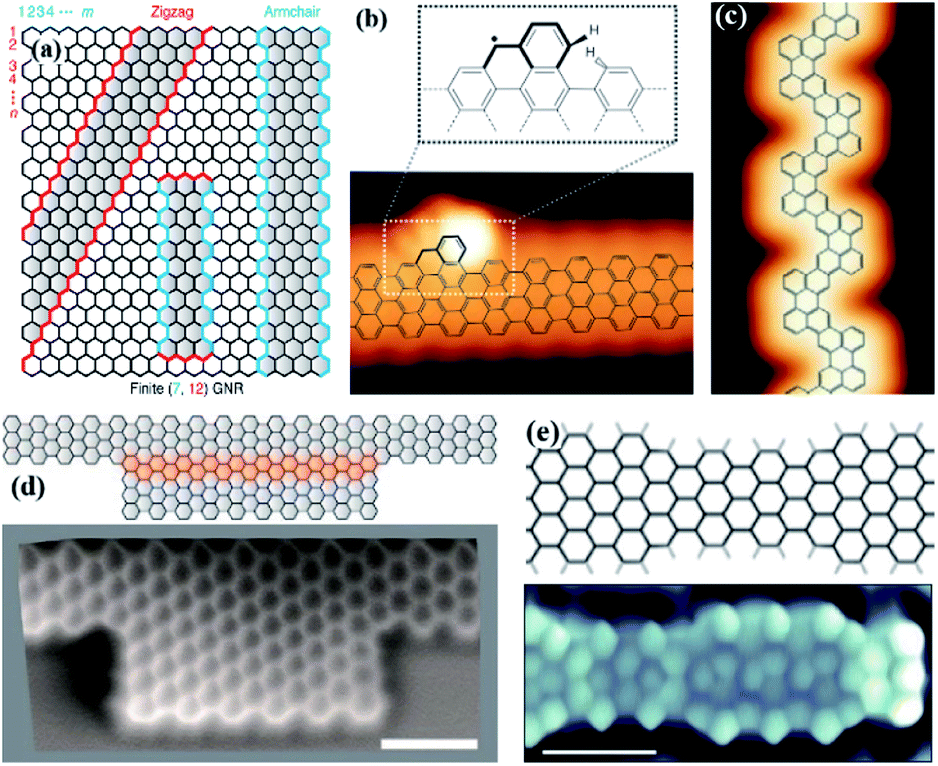 | ||
| Fig. 1 (a) Schematic of the structure of GNRs with zigzag borders (red) and armchair-shaped borders (blue). Indices are used to denote the dimensions of GNRs along the zigzag (m) and armchair direction (n), respectively.38 (b) STM images corresponding edge extensions overlapping the structural model 7-a-GNRs. Scale bar, 1 nm.39 (c) STM topography of sn-8-a-GNRs.40 (d) Schematic of 14-a-GNRs quantum dots formed by the edge fusion of two 7-a-GNRs, and its non-contact atomic force microscopy (nc-AFM) image.41 (e) The local topological electronic state of GNRs and a micrograph of one end of the nanoribbons. Scale bar, 1 nm.42 | ||
1.2 The electronic structure of GNRs
Graphene is a semi-metallic material with a zero band gap. Adjusting the band gap of graphene nanoribbons is a way to open up the properties of GNRs. For example, a-GNRs with a small length has a larger band gap, when both the length and width are small, the band gap of z-GNRs is larger, the double-layer structure has a different band gap than the single-layer structure; doping and adsorption can also control the material structure, etc.43–57 From previous studies, we know that a-GNRs with uniform jagged edges have an energy gap, and the energy gap decreases as the width of the nanoribbon increases. The edge effect is crucial for determining the value of the band gap and the rule of proportionality. The ideal quasi-one-dimensional (1D) quantum confinement is significantly functionalized, which proves that the growth of graphene leads to the formation of silver nanoribbons of different widths and exhibits semiconductor or metallic behavior.58–67 The synthesis method for doping of heteroatom on the surface of GNRs, which is a modulation strategy for GNRs with special electronic properties.The energy spectra of 14 eigenstate nanoribbons with armchair edges are calculated according to the tight-binding equation (Fig. 2(a)). The width of the nanoribbons is N = 200 units.68 The STM image after depositing Si on 475 K substrate and inserting 1 ml of the Si incorporated Au(111) (AuSIL). The differential conductance (dI/dV) spectra recorded on AuSIL show the boundary state of 7-a-GNRs (Fig. 2(b)).69 By performing scanning tunneling spectroscopy (STS5) measurements, the local electronic structure of 13-a-GNRs was determined. The blue line represents the characteristic dI/dV spectra of 13-a-GNRs (Fig. 2(c)).70 The red spectra were acquired at the edge of the borylated section, the green spectra were obtained on Au(111) substrate. The blue arrow and dotted line mark the beginning of the original and borylated part of the conduction band (CB) and the beginning of the original segment of the valence band (VB) (Fig. 2(d)).71 dI/dV spectra obtained at the multi-interval edge of 7–13-a-GNRs can identify the beginning of each band (Fig. 2(e)).72 In dI/dV spectra, CB is 0.20 eV and VB is 0.70 eV, so the electronic band gap is 0.90 eV. This is consistent with density functional theory (DFT) calculations (Fig. 2(f)).73 By performing STS measurements at different locations, it is possible to discover the influence of boron on the embedded electronic structure of the GNRs (Fig. 2(g)).74 The STM scan image of (7, 20) GNRs on NaCl, and dI/dV spectra exhibit two peaks centered at −0.5 V and 1.3 V (Fig. 2(h)).38
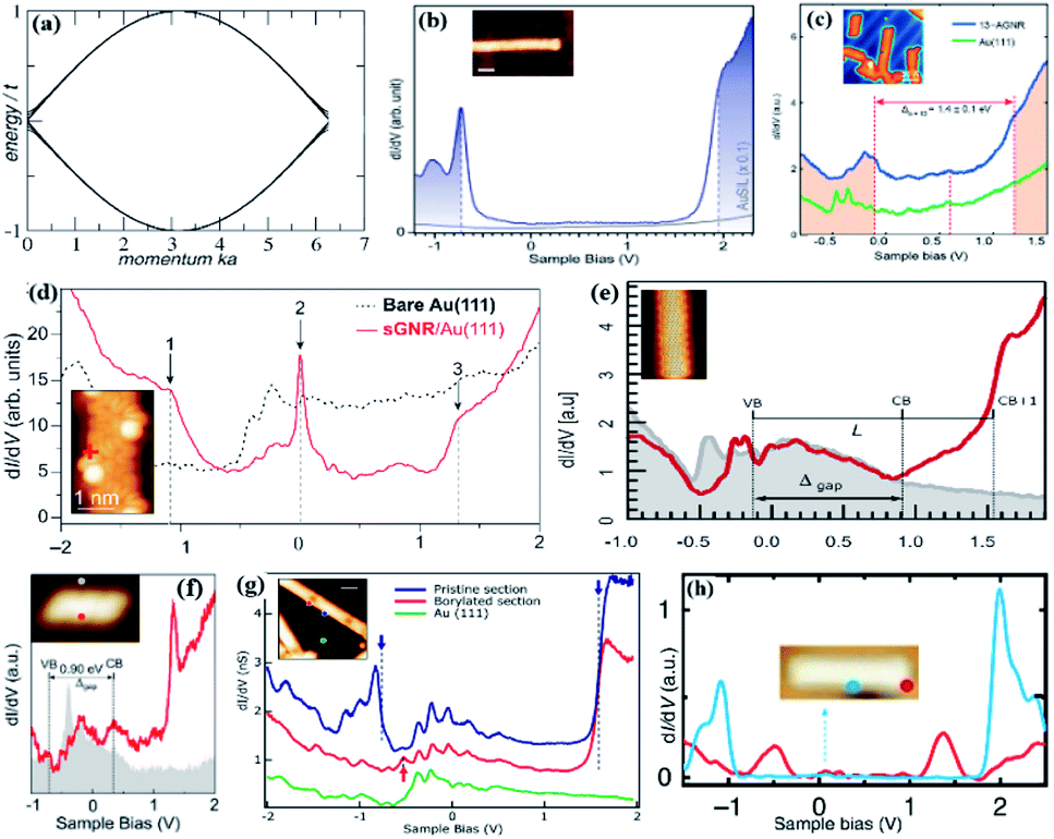 | ||
| Fig. 2 (a) Electron dispersion energy spectrum of GNRs.68 (b) dI/dV spectrum of 7-a-GNRs. The inset shows that Si intercalates the STM image of 7-a-GNRs.69 (c) dI/dV spectra of 13-a-GNRs band gap measured by STM (blue line).70 (d) STM image of a segment of sawtooth-GNRs (s-GNRs). dI/dV point spectroscopy of s-GNRs/Au(111) at the zigzag position marked in the inset. The dashed curve shows the bare Au(111) reference spectrum.71 (e) dI/dV spectrum acquired at the multibay edge of a 7–13-a-GNRs.72 (f) dI/dV spectra taken on nitrogen–boron–nitrogen (NBN)-z-GNRs.73 (g) dI/dV spectra of the mixed GNRs obtained at different locations.74 (h) dI/dV spectra of (7,20) GNRs. Inset: STM image under a bias voltage corresponding to the band gap sample.38 | ||
To better understand the electronic properties of GNRs, researchers use dI/dV spectra for detection. The dI/dV spectra reflect as much as possible the local electronic density of states at a certain energy in real space. According to the width and edge geometry of CNRs, it provides a viable strategy for GNRs with jagged edges and adjustable electronic properties.75–82
2 Electrical properties of GNRs
2.1 Metallicity in GNRs
It is challenging to design and manufacture strong metallic states in GNRs because when graphene is patterned at the nanoscale, lateral quantum confinement and multi-electron interactions can cause electronic band gaps. The bottom-up synthesis method has the latest development, which makes it possible to design and characterize atomically accurate GNRs, but the strategy to achieve GNRs metallicity has been elusive.83–96The half-metal degree is dependent on the system size, different symbols represent z-GNRs of different lengths. When changing the direction of the external electric fields (Eext), the spin polarity of the carriers in the half-metal strip will also be reversed, because the induced potential at the edge changes its sign. When the critical electric field decreases as the width increases, z-GNRs exhibit half-metallicity. Because at this time the electrostatic potential difference between the two edges is proportional to the system size (Fig. 3(a)). If a transverse electric field is applied to the zigzag edge of graphene nanoribbons, its semi-metallic properties are also stable, which provides effective help for exploring graphene-based nanoscale spintronics.45 dI/dV spectra of 5-monomer GNR at different positions. In addition, there are corresponding experimental and calculated conductance diagrams (Fig. 3(b) and (c)).97 The occupied states are at −550 mV and 26 mV. Although all GNRs experimental studies have shown a very wide band gap. They studied that GNRs with a length of 5 nm has reached almost metallic performance at a band gap of about 100 meV. The metal abundance of GNRs was determined experimentally, and its electronic structure was characterized through STM images. The typical dI/dV point spectra were obtained on s-GNRs. A serpentine pattern is observed near the zero-mode band (ZMB) at the valence band edge (V = 0), indicating that the metal state seen in 5-s-GNRs and s-GNRs is very similar (Fig. 3(d)–(g)). This research also provides a useful tool for controlling the metallicity of GNRs and adjusting the electronic structure of GNRs to different physical states. At the same time, it also provides a way for the development of nano-scale equipment and electronic and magnetic phenomena in such one-dimensional metal systems, breaking through the metallic control technology of graphene nanoribbons.71
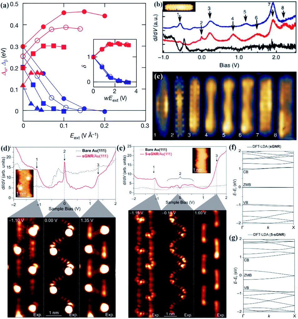 | ||
| Fig. 3 (a) The direct band gap (red line) and indirect band gap (blue line) of GNRs at different widths.45 (b) 5-Monomer long GNRs of dI/dV spectra with a metallic tip.97 (c) Experimental constant-height dI/dV spectra.97 (d) Constant-height dI/dV spectra of s-GNRs conducted at the biases.71 (e) Constant-height dI/dV maps of 5-s-GNRs (right) conducted at the biases.71 (f) Local Density Approximation of Density Functional Theory (DFT-LDA) calculated band structure for (d).71 (g) DFT-LDA calculated band structure for (e). The valence, zero-mode, and conduction bands are labeled VB, ZMB, and CB, respectively.71 | ||
It is possible to adjust the metal abundance in GNRs through the methods described above, inserting the symmetrical superlattice of the zero-energy mode into other semiconductor GNR methods, bottom-up synthesis methods, and so on.
2.2 Topological properties in GNRs
The orange corresponding band E(k,φ) is a non-dispersive band structure with two insulated chain configurations φ = 0 and φ = π/2, π/4. The band (blue) is a gapless metallic phase (Fig. 4(a)).98 The researchers conducted experiments under high vacuum conditions and deposited on the surface of Au(111) single crystals with an atomic-scale precision method. The synthesis of GNRs with alternating widths (Fig. 4(b)).98 The tunnel differential spectroscopy technique is scanned (Fig. 4(c)).98 The topological properties of GNRs are determined, which is a topological band structure that can be adjusted artificially. This has helped to achieve a one-dimensional material bandgap engineering, physics research is also a one-dimensional quantum spin contribution. The research team used molecular precursors to assemble experiments and obtained atomic-scale GNRs, which is consistent with the predicted valence electron structure in the Su–Schrieffer–Heeger (SSH) theoretical model (Fig. 4(c) and (e)). At the same time, it was found that there is a controllable periodic coupling in the topological boundary state at the junction of the GNRs.42 Another researcher discovered that a peak was found at the Fermi energy (EF), which is called a 1D topological surface state. This state may provide ballistic and spin-polarized transport channels (Fig. 4(f) and (g)).99 The existence of the kink state in the (positive and negative) electric field configuration (red curve) results in high conductance inside the band gap, while the blue curve σj is in the negative electric field configuration. The conductivity is low (Fig. 4(h) and (i)). This research uses electronic control to create a 1D topological conductive channel in bilayer graphene (BLG). By combining a narrower junction with a larger band gap, allows the kink valley electronic device to work at non-low temperature. This structure makes it possible to realize potential-controlled quantum dots with few electrons and opens the door to the edge states and the domain wall physics of the BLG quantum Hall system.100 | ||
| Fig. 4 (a) Implementing the SSH model in GNRs.98 (b) Surface chemical synthesis method results in atomically accurate GNRs.98 (c) Tight-binding-simulated charge-density maps plot of VB top, E = 0 eV, and CB bottom.98 (d) A bond-resolved STM image of 7–9-a-GNRs superlattice shows the bond-resolved structure of the heterojunction interface.42 (e) DFT-LDA energy band structure of 7–9-a-GNRs superlattice.42 (f) Various STS spectra taken on the edge of the z-GNRs from seven different ribbons.100 (g) High-resolution STM image of the edge of the z-GNRs (+1.9 V, 0.1 nA).100 (h) The junction conductance σj at a function of VSi at fixed values of DR from DR from −0.4 nm−1 to 0.4 V nm−1.101 (i) σj versus VSi along the yellow dashed lines marked in the upper (blue curve) and lower (red curve) panels.101 | ||
The topology of GNRs can be further modified by dopants. The GNRs topological insulators are designed by experimental methods, and they have achieved strange topological states. The theoretical calculations are consistent with the experimental results. This precise regulation of the energy band of 1D materials based on electronic topology lays the foundation for the development of quantum computing technology in the future.101–121
2.3 Transport characteristics of GNRs
Johannes et al. have studied a variety of GNRs and discovered their special transport properties. When studying the asymmetric sidewall nanoribbons between the upper and lower edges caused by the edge morphology, it was found that a unique isolated transport channel can be produced. When the moving tip is connected to the lower edge of the belt (Fig. 5(a)),122 the conductance is e2/h. When the tip moves from the edge to the whole, two platforms with higher conductivity will appear, the values of which are close to 4e2/h indicating transmission through an additional 4 times degenerate ballistic channel. A group of researchers presented strong evidence for a single-track ballistic transmission in long epitaxial GNRs (Fig. 5(b)).123 This means that both spin and valley degeneracies have increased. On the other hand, the conductance step of 4e2/h implies that the transport of sub-bands was induced by spin generation and valley degeneracy constraints, such as those expected in the original zigzag nanoribbons. | ||
| Fig. 5 (a) Conductance measured for a fixed distance L = 70 nm. Inset: I–V-curves measured at of the GNRs.122 (b) Resistance versus probe spacing L.123 (c) STM image of the etched graphene.124 (d) Temperature-variable transport measurement results of z-GNRs under a 9 T magnetic field.124 (e) Temperature-variable transport measurement results of disordered edge GNRs under a 9 T magnetic field.124 | ||
When the team conducted research on the z-GNRs, they discovered that the z-GNRs of different widths were processed on hexagonal boron nitride (h-BN) insulating substrates. Under the combined action of the strong magnetic field and the size effect of the nanoribbons, the “edge states” with a fill factor of zero (V = 0) were successfully insulated. A conductance peak related to the edge state was observed, which was not changing with temperature and magnetic field of robustness. At the same time, through non-local measurements, a voltage signal was also observed under zero magnetic field, and its energy position was consistent with the conductance peak under magnetic transport, further confirming that the edge states are involved in conduction. In addition, in the comparative samples of GNRs with disordered edges, this edge transport feature did not appear, which confirms that the edge conductivity is unique to the zigzag edge (Fig. 5(c)–(e)).124
The above series of interactions can provide new ideas for future development, including interfaces with lateral heterostructures, systems with emergent topological effects, and quantum Hall effects. Regardless of the source of the materials, in the future electronic products of GNRs, ballistic transport at room temperature will play a vital role.125–142
2.4 Electrical conductivity properties of GNRs
The conductivity between the feature is used to study the interaction of atomic structure and electronic properties of GNRs. This kind of prospect will provide help in new cross-two-dimensional materials in the future.143–156 Transport measurements show that the band gap size of sub-7-nm-wide z-GNRs is inversely proportional to its width, while the band gap–width relationship of narrower a-GNRs exhibits volatility. Obvious conductance peaks are observed in the 8–10 nm wide z-GNRs transmission curve (Fig. 6(a)), but not in most of a-GNRs. At the same time, magnetic transport studies have shown that z-GNRs exhibit lower permeability, but a-GNRs have higher permeability. The successful preparation of h-BN surface embedded chirality-controllable GNRs provides a new way for complex nano-integrated circuits.157 The GNRs prepared by Joule heating can obtain GNRs with a width of about 10 nm. During the reduction process, the conductance nonlinearity of GNRs was displayed as a function of width (Fig. 6(b)).158 | ||
| Fig. 6 (a) Graph of the relationship between conductivity (G) and the back gate voltage (Vgate) of the ∼5 nm wide a-GNRs device at different temperatures.157 (b) dI/dV as a function of bias voltage. Inset: TEM image of 1.6 nm wide graphene.158 (c) The conductance of GNRs when the Joule heating value increases.159 (d) Measure the conductivity diagram of a single molecule.160 (e) Conductivity of GNRs with different layers.161 (f) dI/dV spectra as a function of DC bias current and vertical magnetic field.162 | ||
This proves that the known structure of GNRs, the opening and conductance differential characteristics of the band gap exists. They obtained the thinnest GNRS structure, with a width of about 1.6 nm, and 400 meV is observed by transportation measurement. The inherent electronic properties of GNRs can be studied in this way. The research team performed spatial mapping of the electronic structure of the long and narrow GNRs adsorbed on the Au(111) surface (Fig. 6(c)).159 This study provides an in-depth understanding of the reconstruction mechanism of a single nanoscale device detected in situ. In the sub-10 nm-wide GNRs device, lattice disorder and bonded double-layer edges are observed immediately after the pattern is formed. As the Joule heating increases, the GNRs continue to recrystallize while maintaining the combined double-layer edge. Although the width becomes narrower, its inherent conductivity is increased. It was found that the device width was reduced by nearly 3 times, the intrinsic conductivity doubled during the recrystallization process to 2.7e2/h, which indicated the limitation of the traditional pattern/etching process and the potential of Joule-heat recrystallization.
Some studies have discovered the electrical conductivity properties of single GNRs and linked them to the atomic structure and electronic state. When systematically measuring the stretching curves of different bias voltages (i.e., the electrode electron energy relative to the movement of the GNRs), different slopes can be obtained (Fig. 6(d)),160 and each bias voltage has a characteristic attenuation constant. It is found that when the bias value increases, the slope of the conductance will decrease, so the conductance will increase. This proves the importance of the edge state and plane geometry. The researchers made controllable single-layer and few-layer GNRs with a width of less than 15 nm (Fig. 6(e)). The conductivity of double-layer GNRs is about GFL(w) ≈ 0.75(e2/h)w, the conductivity of single-layer GNRs is about 5 times that of the single-layer. The high conductivity of the few-layer GNRs is due to the bonding edge, which provides a stable structure and additional conduction channels. Single-layer GNRs form the armchair end edge after the current annealing, providing a way to prepare edge-specific GNRs.161 In experiments, it was found that the rhombohedral stacked trilayer graphene (ABC-TLG) and h-BN superlattice showed a Mott insulation state below 20 K. It is expected that the electronic behavior in the ABC-TLG/h-BN superlattice will very much depend on the interaction between the electronic interaction and the microstrip bandwidth. The magnetic field obviously inhibits the apparent superconductivity, and the superconductivity almost disappears, showing a wealth of adjustable behavior (Fig. 6(f)).162
People expect to effectively control the conductivity of these systems through the edge structure, whether in the bottom-up surface polymerization process or through the substrate. These developments will open up new directions for the band gap engineering of the next generation of nanoelectronics.
2.5 Other electrical properties of GNRs
Wei et al. studied the first single GNR electron emission. Through the typical electron transfer characteristics of GNRs, when the driving voltage is 3 V, high emission density can be achieved (Fig. 7(a) and (b)).163 Electrons are driven out of a single GNR, and the emission current increases exponentially with the driving voltage. A group of research teams obtained the electrochemical lithium absorption capacity of carbonaceous 1D GNRs by decompressing the original multi-walled carbon nanotubes (MWCNTs). Studies have found that oxidized GNRs (ox-GNRs) are superior to other materials in terms of energy density. The reversible and irreversible capacities increase of ox-GNRs indicates that the presence of oxygen in GNRs induces more stable formation, chemically bound solid electrolyte interface (SEI) (Fig. 7(c) and (d)).164 This powerful SEI rich in Li elements may prevent electrode degradation and enhance the storage capacity of the electrode. The reversible capacity of ox-GNRs is in the range of 800 mA h g−1, the capacity loss per cycle in the early stage is about 3%, and the loss rate in the subsequent cycles gradually decreases. | ||
| Fig. 7 (a) Two-terminal transmission characteristic curve.163 (b) Different GNR curve measurements under different driving voltages.163 (c) The charge and discharge curve of medium carbon microbeads (MCMB) graphite.164 (d) Charge and discharge curve of ox-GNRs.164 (e) Acoustic current at several surface acoustic waves (SAW) frequencies.165 (f) Calculation diagram of attenuation coefficient.165 | ||
The researchers studied the acoustoelectric effect in GNRs and showed that at room temperature, GNRs with a physical width as small as 200 nm can generate acoustic currents. In an 300 μm × 3 mm array composed of 500 nm wide GNRs, when the surface acoustic wave frequency is 442 MHz, the measurement found an acoustic current of as high as ∼5.5 μA (Fig. 7(e)).165 It is found that the acoustic current attenuation coefficient increases as the width decreases and the conductivity increases as the bandwidth decreases from 600 nm to 350 nm (Fig. 7(f)).165 From the induced acoustic current density equation, it is concluded that as the bandwidth decreases, not only the conductivity increases but also the mobility in the band. Because, during the preparation process, the increase in doping along the rough edges of the damage causes an increase in the acoustic current.
In just a few years, the development of GNRs has become a hot spot among the scientific community. We believe that these discoveries of electrical properties, acoustoelectric effects, electron emission, electrochemistry, acoustoelectric effects, electrocatalytic activity and other properties will eventually be widely used in various researches.166–169
3 Applications based on GNRs
3.1 The field-effect transistor (FET)
A semiconductor device can control the output loop current by controlling the electric field effect of the input loop, FET.166–184In 2013, researchers proved that by introducing edge defects, to achieve a higher pH response of graphene FET, edge defects can be introduced. The decrease in GNR width increases the pH response. In the original graphene FET and 100-nm-wide GNR devices, the lowest sensitivity values (about 0 mV pH−1) and highest (30.6 mV pH−1) were respectively found (Fig. 8(a)).185 When the ratio of side length to the specific surface area increased from 0.04 μm−1 to 20 μm−1, the pH response increased from 4.2 mV pH−1 to 24.6 mV pH−1 (Fig. 8(b)).185 Obviously, increasing the edge defects can effectively improve the pH response, by reducing the GNR width. Moreover, the change of pH value can cause the reversibility of the Dirac point, which indicates that hydroxide ions can be adsorbed on the edge defects of GNRs through physical methods.
 | ||
| Fig. 8 (a) Histogram of the pH response of the device.185 (b) Average pH response for different edge ratios.185 (c) Output characteristic graph under different back gate bias voltages.186 (d) Transmission characteristics of 7-a-GNRs-FET.186 (e) 9-a-GNRs-FET: Id–Vg characteristics of the scaled.187 (f) Graph of Id–Vg. Inset: Schematic diagram of 9-a-GNRs-FET.187 (g) The output characteristic graph of GNRs-FET.188 (h) FET behavior in the p-type channel.188 (i) Analytical modelling: NDR-FET behavior.188 (j) Raman spectrum of GNRs channel in GNRFET.189 (k) The output characteristics of GNRFET at room temperature.189 (l) Transmission characteristics of GNRFET at room temperature.189 | ||
In 2018, Passi and other researchers conducted research on 7-a-GNRs FETs. The atomically accurate and highly aligned 7-a-GNRs can synthesize back-gate transistors using a bottom-up method. The channel length of FETs is approximately 30 times the length of the 30–40 nm nanobelt. Due to the high density of GNRs, it can be assumed that the transmission is much higher than the percolation threshold. The long-channel transistor shows the largest Ion/Ioff current ratio (Fig. 8(c) and (d)). These changes are only part of the definition. The performance of devices with graphical a-GNRs or optimized sources will also be improved, which provides an effective way for the development of GNRs integrated devices and circuits.186 Another group of researchers used a high-κ gate dielectric and 9-atom wide GNR channel materials, short channel (about 20 nm) devices were prepared; high-through-current and high Ion/Ioff ∼ 105 FETs were realized at room temperature (Fig. 8(e) and (f)).187 If you want to increase the transparency of the barrier, you can increase the gate field near the contact. It is proved that the a-GNRs synthesized from the bottom up are used to successfully fabricate high-performance short channel FETs. Researchers experimentally proved the working of atomic thin GNRs tunneling field-effect transistors (TFETs) at room temperature. The clear and repeatable negative differential resistance (NDR) can be observed; NDR tunnel current density is ∼1 mA μm−1 (Fig. 8(g)).188 NDR disappears under the positive drain voltage (Fig. 8(h)), and GNR-TFET output characteristics (Fig. 8(i)).188 Because of the tunneling of carriers between bands, in the transistor characteristics of the gated GNRs p–n junction, NDR shows repeatability and reversibility. GNR conclusive evidence is adjustable NDR, the bandgap of the lithographically-defined presence and the thinnest Esaki diode. It provides help for the thinnest and scalable development of low-power TFET.
Researchers have fabricated field-effect transistor devices by flattening carbon nanotubes. The field-effect mobility of the device reached 2443 cm2 V−1 s−1, the on-state conductivity was 7.42 mS and the switching ratio reached >104 (Fig. 8(i)–(l)). The band gap of the band is estimated to be ∼0.49 eV. Research data show that, compared with the previous use of graphene nanoribbons or carbon nanotubes to make arrays, the nanoribbons obtained using this method can better meet the needs of integrated circuits. This kind of GNR material with a very small transistor size will have a huge impact on the application of integrated circuits.189
In summary, it is found that the bottom-up synthesized GNRs devices are high-performance application devices. The research on the growth mechanism of GNRs has improved the average length of GNRs and the yield of devices. Performance is also improved when edge defects are introduced. With the advantages of low power consumption, stable performance, and strong anti-radiation ability, field-effect devices have gradually replaced triodes in integrated circuits.
3.2 Supercapacitor based on GNRs
Between the traditional capacitor and rechargeable battery, there is a new type of energy storage device, the supercapacitor. It not only has the characteristics of fast charging and discharging of capacitors but also the energy storage characteristics of batteries.190–200Some researchers have analyzed the availability of carbon nanorods and GNRs. In the steady-state cyclic voltammogram of GNRs, the regular rectangular shape without any redox peaks shows its excellent capacitance performance (Fig. 9(a)).201 As the scan rate increases, the specific capacitance attenuates by 35% (Fig. 9(b)). The outstanding performance of supercapacitors exhibited by such excellent GNRs has progressed the development of two-dimensional carbon materials.201 In this way, materials with useful functions can be synthesized. Another group of researchers aimed at the preparation and processing of 1D single-layer GNRs. Electrochemical impedance spectroscopy and cyclic voltammetry show that the average capacitance of 75 μF cm−2 at 100 kHz to 1.16 mF cm−2 at 1 Hz and 0.35 ± 0.04 mF cm−2 (Fig. 9(b) and (c)),202 much higher than the upper limit of the capacitance of the carbon-based electrode. Theoretical calculations and experimental results show that by adjusting the structural constraints and doping appropriate functional groups into GNRs at the edges of the reaction, the limitations encountered in charge storage applications can be broken. The high-area capacitance greatly improves the quality control of GNRs, which can solve the newer observation energy storage device and provide help for the study of lateral structural constraints. Klaus of the University of Mainz in Germany used a bottom-up method to synthesize a-GNRs film. This film can be used as an electrode material for micro supercapacitors (MSC) because of its excellent volume capacitance and ultra-high power density. Studies have shown that the electrochemical performance of MSC may be related to the carrier mobility in different GNRs, 5-a-GNRs ≫ 9-a-GNRs > 7-a-GNRs (Fig. 9(e)).203 The power density of a-GNRs in MSCs is higher than that of traditional supercapacitors, and more than one order of magnitude higher than aluminum electrolytic capacitors (Fig. 9(f)). The synthesized a-GNRs provide a practical energy storage system for this new one-dimensional carbon material. Such microdevices have ultra-high power density and excellent volumetric capacitance.203
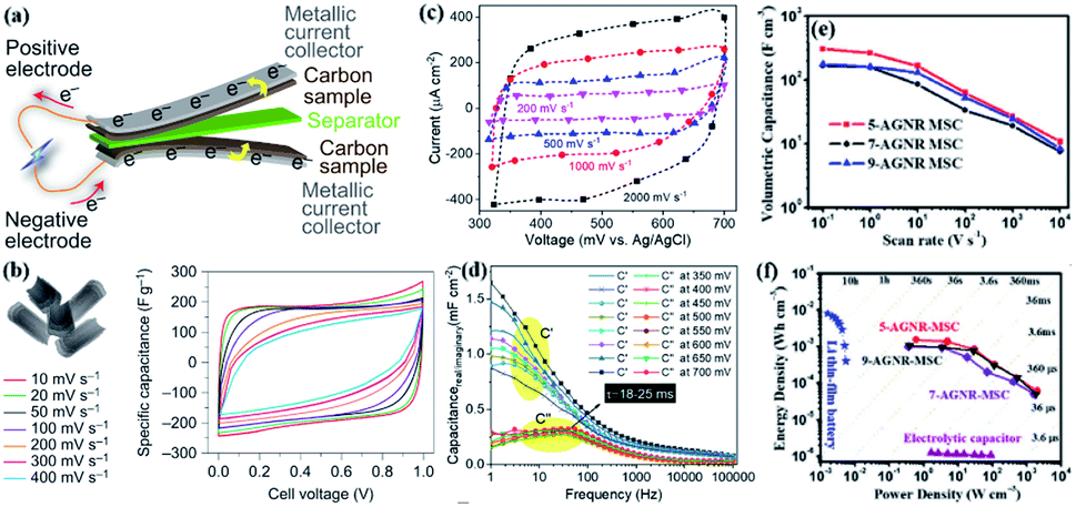 | ||
| Fig. 9 (a) Electrochemical results of GNRs under different bias voltages.201 (b) The relationship between cell voltage and specific capacitance at different scanning rates.201 (c) Comparison chart of current–voltage characteristics.202 (d) Schematic of supercapacitor.202 (e) The relationship between volumetric capacitance and scan rate for each width of a-GNRs.203 (f) Comparison of power density and energy density of electrolytic capacitors in MSC devices with different widths of a-GNRs.203 | ||
The exploration of energy storage in high-speed supercapacitors has always been a hot spot in the study of GNRs. Whether it is physical or chemical methods, precise synthesis will have an impact on the electrochemical properties of GNRs.
3.3 Electrocatalyst based on GNRs
The research team decompressed MWCNTs and synthesized a zigzag edge graphene nanofiber skeleton for oxygen reduction in an electric discharge material exchange membrane fuel cell. Zigzag carbon exhibits peak mass densities of 0.161 W cm−2 and 520 W g−1 (Fig. 10(a) and (b)),204 which is better than most metal electrocatalysts. In an acidic environment, the calculation and experimental results show that the oxygen reduction reaction (ORR) electrocatalytic activity of tortuous carbon atoms is higher than that of oxidizing tortuous carbon and carbon atoms near the cavities (Fig. 10(c)).204 The experimental results are the same as the theoretical calculation results, which indicate that this electrocatalyst can be used in inexpensive and good performance proton exchange membrane fuel cells. Due to the higher electrocatalytic activity of the zigzag carbon atoms on ORR, it can play a role in PEMFC applications. It will also be a challenge to synthesize GNRs with jagged edges in the future. Another research team used carbon-based electrocatalysts containing Fe and N elements and graphene nanoribbon@carbon nanotube (Fe–N/GNR@CNT) material as the air-cathode electrocatalyst of the microbial fuel cell (MFC) for the first time. Fe–N/C and industrial Pt/C have similar power generation capacities. Under the condition of different nitrogen doping, the specific surface area of Fe–N/C is also different, indicating that the ORR electrocatalytic activity in the sample is mainly affected by the heteroatom-doping level and the number of active bits (Fig. 10(d)).205 The test was carried out in a 50 mM phosphate buffer saline solution (PBS) electrolyte, and the electron transfer number of Fe–N/C was 3.57 (Fig. 10(e)),205 The electron transfer number of Pt/C is 3.90 (Fig. 10(f)).205 These indicate that the ORR process is mainly dominated by 4 electrons. The presence of Fe, pyridine-N, graphite-N and oxygen-containing groups in GNR@CNT may make the electrocatalyst show good ORR performance. Because of the existence of these doping factors, the electrocatalyst has good ORR performance and its low-cost characteristics, so that GNR@CNT-based materials have become metal catalyst materials to replace other metals. | ||
| Fig. 10 (a) Graphene nanoribbon polarization curves as a function of power density and current density of the surface with cathode catalyst loading of 0.25 mg cm−2.204 (b) Graphene nanoribbon polarization curves as a function of power density and current density of the surface with cathode catalyst loading of 0.50 mg cm−2.204 The model of the carbon atom (inset) and the corresponding free energy diagram, (c) carbon atoms at the zigzag edge.204 (d) Adsorption–desorption isotherms under different nitrogen-doping levels.205 (e) Linear sweep voltammetry (LSV) curve of Fe–N/C at different speeds.205 (f) LSV curve of Pt/C at different speeds.205 | ||
Precious metal catalysts have always been an obstacle in the field of research.206–212 This kind of non-noble metal and metal-free catalyst are ideal materials. The low-cost material will be widely used.
3.4 Electrochemical sensor based on GNRs
Casero's research group of the Autonomous University of Madrid synthesized chevron-like GNRs based on solution synthesis, and developed a new type of electrochemical sensor to measure the neurotransmitter epinephrine (EPI). On the sensor surface, electrochemical impedance spectroscopy is used to determine the charge transfer that occurs at the electrode interface. This sensor is used to measure EPI. The reduction peak corresponding to the conversion of adrenaline to white adrenaline is used as the analysis signal (E = −0.25 V) instead of the oxidation peak (E = +0.6 V) reported in the literature. Reduce interference factors. The electrochemical response of GNRs deposited on glassy carbon electrodes (GCE) sensors to increasing EPI concentration (Fig. 11(a)).213 Scientists concluded a linear relationship regarding the modification of electrodes. This shows that when a diffusion-limited transport process is observed, the charge transfer can be significantly improved (Fig. 11(b)).213 The research results show that this nanobelt exhibits reliable electrocatalytic activity in the determination of EPI. The linear concentration range is 6.4 × 10⁻⁶ M to 1.0 × 10⁻⁴ M (Fig. 11(c)).213 By measuring the EPI in the drug sample, its applicability was evaluated, and the result was satisfactory. These results indicate that chemically synthesized GNRs can be successfully applied to the development of electrochemical sensors. The new type of electrochemical sensor synthesized by solution has been well discovered in the laboratory at present, and the follow-up progress is still being strengthened.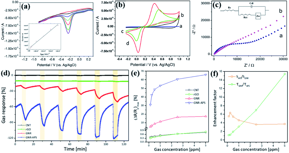 | ||
| Fig. 11 (a) Differential pulse voltammetry (DPV) response of materials in phosphate-buffer solution containing different concentrations of EPI.213 (b) Cyclic voltammogram of GCE electrode with/without GNRs modification in 0.1 M PBS at pH = 7.0.213 (c) Comparison of electrochemical impedance spectroscopy of GCE electrode with/without GNR-modification, the amplitude is ±10 mV.213 (d) The real-time sensing performance of each sensor to various concentrations of NO2 from 0.125 to 5 ppm.214 (e) The sensor is the maximum resistance change ((ΔR/Rb)max (%)) of NO2 concentration maximum value.214 (f) The relationship between the gas concentration and enhancement factor after APS functionalization.214 | ||
Some researchers have studied the application of GNRs in chemical sensors. The chemical modification of aminopropyl silane (APS) molecular edge sites will affect the electrical channel properties of GNRs, thereby improving the sensing performance of GNR sensors. The APS-functionalized GNR sensor has a sensitivity maximal resistance change ((ΔR/Rb)max) of up to 30% when the concentration of nitrogen dioxide (NO2) is 0.125 ppm, and the response time is ultra-fast (about 6 seconds) (Fig. 11(d)).214 The response amplitude of each sensor gradually increases with the increase of NO2 concentration (Fig. 11(e)).214 The enhancement factors of GNRs sensor sensitivity and response time before and after APS functionalization is calculated. When the NO2 concentration is higher, the doping effect of APS is better in response time (Fig. 11(f)). Edge-functionalized GNRs have a larger gas response, and GNR-APS sensors also show higher sensitivity, which proves the importance of edge-functionalization of GNRs to chemical sensors.214
This sensitive sensor material makes GNRs useful for devices such as transistors. Increasing its conductivity by several orders of magnitude is also beneficial for sensors. Most electrochemical sensors use metal oxide semiconductors as basic materials. Similar sensors include those made of microfluidic biosensors, nanocomposite network membranes and other nanomaterials. These instruments affect all aspects of our lives: medical blood testing, portable photoelectric equipment, food freshness testing, and drug testing in high-risk environments. This kind of portable instrument is easier to carry than the instrument based on GNR material mentioned above. However, some sensors still need long-term research on the production road.215–226
3.5 Composite material on battery
The research team successfully synthesized high-performance lithium-ion battery composite anodes by evenly distributing SnO2 nanoparticles on or in a stack of conductive GNRs. The composite has a high reversible discharge capacity of 1130 mA h g−1. In the 50th cycle, when the current density is 0.1 A g−1, its discharge capacity remains at about 825 mA h g−1 (Fig. 12(a)).227 At a current density of 2 A g−1, the specific capacity of the composite was 580 mA h g−1 (Fig. 12(b)),227 which is much higher than the theoretical capacity of graphite. The high-capacity SnO2 composite material has helped the development path of lithium storage based on GNRs-based composite materials and other metal oxides. However, there are still certain difficulties in the preparation and synthesis. Cui's research team designed graphene–ZnO composite electrodes, which can be used in nickel–zinc secondary batteries. They cut graphene into short nanoribbons in situ, effectively fixing a large number of zinc atoms on its surface. In the test cycle, the mass ratio of graphene to zinc oxide is 31![[thin space (1/6-em)]](https://www.rsc.org/images/entities/char_2009.gif) :19 (38% ZnO). The electrochemical performance is very stable, and the cycle life of the battery is far greater than 10000 times (Fig. 12(c)).228 When the mass ratio of graphene to zinc oxide is 80.7% and the number of cycles is greater than 1700, the midpoint discharge capacity decreases slightly, indicating that the cycle stability is weaker than that of 38% ZnO (Fig. 12(d)). For traditional Ni–Zn batteries, the newly designed Ni–Zn batteries have excellent discharge capacity and easy-to-operate preparation methods. This superior electrochemical performance is very useful in the electrochemical field.228
:19 (38% ZnO). The electrochemical performance is very stable, and the cycle life of the battery is far greater than 10000 times (Fig. 12(c)).228 When the mass ratio of graphene to zinc oxide is 80.7% and the number of cycles is greater than 1700, the midpoint discharge capacity decreases slightly, indicating that the cycle stability is weaker than that of 38% ZnO (Fig. 12(d)). For traditional Ni–Zn batteries, the newly designed Ni–Zn batteries have excellent discharge capacity and easy-to-operate preparation methods. This superior electrochemical performance is very useful in the electrochemical field.228
 | ||
| Fig. 12 GNRs and SnO2 composite materials: (a) the capacity retention and coulombic efficiency at a rate of 100 mA g−1.227 (b) the ability of composite electrodes of various current densities.227 (c) The midpoint discharge capacity of the graphene–ZnO hybrid electrode (38% ZnO).228 (d) The midpoint discharge capacity of the graphene–ZnO hybrid electrode (80.7% ZnO).228 (e) Comparison of the cycling performance at 200 mA g−1.229 | ||
Xu's research team has discovered a new type of cathode with GNRs decorated with RuO2 catalysts by decompressing MWCNTs. The decorative RuO2 catalyst was obtained by decompressing MWCNTs. RuO2 introduced by a simple drip method enhanced the kinetics of oxygen evolution reaction and significantly reduced the charge overpotential. More importantly, the lithium–oxygen battery with RuO2 modified graphene nanoribbon cathode has good 424 cycle stability at a capacity of 1000 mA h g−1 (Fig. 12(e)).229 Due to the different substrate structures, Li2–O2 deposited on GNRs and Li2–O2 deposited on MWCNTs have completely different surface morphologies. This provides development assistance for the high-efficiency air electrode design of high-performance lithium–oxygen batteries. It will also provide help in subsequent research on battery energy efficiency and cycle life.
The research on GNRs composite materials has provided an effective design for traditional batteries, both the cycle life and discharge capacity have been significantly improved. Researchers will continue to explore their characteristics.230–234
4 Conclusion
GNRs exhibit special electrical properties through their unique electronic structures. Researchers have found that GNRs themselves have atomic-level precision and stability. When the width, boundaries, defects, stress, surface adsorption, doping of other atoms, etc. of GNRs are adjusted, slight changes will cause changes in the electronic structure and electrical properties of GNRs.In this work, we have summarized the latest research progress on the electrical properties of GNRs and the application prospects of GNRs. The electrical properties of GNRs: metallic, topological, transport, conductivity, acoustoelectric effect, electron emission, electrochemistry, electrocatalytic activity, etc. are summarized. GNRs not only have broad prospects in the field of electricity, but also have outstanding research in the fields of optics, heat, and mechanics.
We have also obtained GNRs as basic materials suitable for FETs, electrochemical sensors, supercapacitors, electrocatalysts, and other electronic devices. The application of GNRs to a variety of electronic devices broadened the ideas and methods. For example, GNRs are suitable for the production of high-performance electronic products as a substitute for silicon; the edge effect of GNRs can be controlled to change the metallicity of devices; GNRs have good conductivity and can produce large-scale, cheap and high-conductivity integrated circuit devices; GNRs that are used as the composite material in the battery have superior energy conversion efficiency and so on. When exploring the width-dependent semiconductor band gap driven by the quantum confinement effect, the closed state in electronics is realized, which contributes to the study of quantum confinement, and at the same time provides substantial help in the follow-up low-power electronic technology. GNRs have a large battery capacity and long charging time, which solves the shortage of energy batteries in the past and paves the way for the future application of the new energy battery industry. Especially, supercapacitors based on GNRs, GNRs have excellent conductivity and high specific surface area performance. With the development of industry and productivity, high-precision supercapacitors are prepared to meet actual needs. For example, high power density, long cycle life, low and high-temperature resistance, higher voltage, high safety supercapacitors can be used in good energy storage devices, such as truck starting, windmills, and electric meters.
Compared with traditional research, in recent years, researchers have devoted themselves to creating new materials. The synthesis is limited to small fragments, and a large number of production methods are yet to be explored. The research in the field has great potential, especially related to electrical characteristics. GNRs have bright application prospects in many fields such as electronic devices.
Author contributions
The content and design: Jingang Wang and Yi Zou; writing manuscripts: Jingang Wang; original writing: Wenjing Bo.Conflicts of interest
There are no conflicts to declare.Acknowledgements
This work was supported in part Scientific research fund project of Educational Department of Liaoning Province (No. L2019028). Fundamental Research Funds for the Central Universities and talent scientific research fund of LSHU (No. 2018XJJ-007).Notes and references
- L. Gao, C. Ma and S. Wei, et al., Applications of Few-Layer Nb 2 C MXene: Narrow-Band Photodetectors and Femtosecond Mode-Locked Fiber Lasers, ACS Nano, 2021, 15, 954–965 CrossRef CAS PubMed.
- J. Pei, J. Yang and T. Yildirim, et al., Many-Body Complexes in 2D Semiconductors, Adv. Mater., 2019, 31, 1706945 CrossRef PubMed.
- Y. Zhang, P. Huang and J. Guo, et al., Graphdiyne-Based Flexible Photodetectors with High Responsivity and Detectivity, Adv. Mater., 2020, 32, 2001082 CrossRef CAS PubMed.
- A. C. Ferrari, Raman spectroscopy of graphene and graphite: Disorder, electron–phonon coupling, doping and nonadiabatic effects, Solid State Commun., 2007, 143, 47–57 CrossRef CAS.
- G. Binnig and H. Rohrer, Scanning tunneling microscopy, Surf. Sci., 1983, 126, 236–244 CrossRef CAS.
- G. Doyen, E. Koetter and J. P. Vigneron, et al., Theory of scanning tunneling microscopy, Appl. Phys. A: Solids Surf., 1990, 51, 281–288 CrossRef.
- D. A. Muller, Structure and bonding at the atomic scale by scanning transmission electron microscopy, Nat. Mater., 2009, 8, 263–270 CrossRef CAS PubMed.
- P. Hashemi, A. Afkhami and B. Baradaran, et al., Well-orientation strategy for direct immobilization of antibodies: development of the immunosensor using the boronic acid-modified magnetic graphene nanoribbons for ultrasensitive detection of lymphoma cancer cells, Anal. Chem., 2020, 92, 11405–11412 CrossRef CAS PubMed.
- J. Sun, S. Feng and X. Wang, et al., Regulate of Electronic Structure of Graphene Nanoribbon by Tuning Long-Range Dopant-Dopant Coupling at Distance of Tens of Nanometers, J. Phys. Chem. Lett., 2020, 11, 6907–6913 CrossRef CAS PubMed.
- T. Dienel, S. Kawai and H. SöDe, et al., Resolving Atomic Connectivity in Graphene Nanostructure Junctions, Nano Lett., 2015, 5185–5190 CrossRef CAS PubMed.
- C. Sánchez-Sánchez, T. Dienel and O. Deniz, et al., Purely Armchair or Partially Chiral: Non-Contact Atomic Force Microscopy Characterization of Dibromo-Bianthryl-Based Graphene Nanoribbons Grown on Cu(111), ACS Nano, 2016, 10, 8006–8011 CrossRef.
- S. J. Heerema, L. Vicarelli and S. Pud, et al., Probing DNA Translocations with Inplane Current Signals in a Graphene Nanoribbon with a Nanopore, ACS Nano, 2018, 12, 2623–2633 CrossRef CAS PubMed.
- S. H. Kang, et al., A Robust Highly Aligned DNA Nanowire Array-Enabled Lithography for Graphene Nanoribbon Transistors, Nano Lett., 2015, 15, 7913–7920 CrossRef CAS PubMed.
- Q. Xu, T. Ma and M. Danesh, et al., Effects of edge on graphene plasmons as revealed by infrared nanoimaging, Light: Sci. Appl., 2017, 6, e16204 CrossRef CAS PubMed.
- P. H. Jacobse, A. Kimouche and T. Gebraad, et al., Electronic components embedded in a single graphene nanoribbon, Nat. Commun., 2017, 8, 119 CrossRef CAS PubMed.
- J. A. Rodríguez-Manzo, Z. J. Qi and A. Crook, et al., In Situ Transmission Electron Microscopy Modulation of Transport in Graphene Nanoribbons, ACS Nano, 2016, 10, 4004–4010 CrossRef PubMed.
- Y. Pak, S. M. Kim and H. Jeong, et al., Palladium-decorated hydrogen-gas sensors using periodically aligned graphene nanoribbons, ACS Appl. Mater. Interfaces, 2014, 6, 13293–13298 CrossRef CAS PubMed.
- V. Volman, Y. Zhu and A. R. O. Raji, et al., Radio-frequency-transparent, electrically conductive graphene nanoribbon thin films as deicing heating layers, ACS Appl. Mater. Interfaces, 2014, 6, 298–304 CrossRef CAS PubMed.
- K. Nakada, M. Fujita and G. Dresselhaus, et al., Edge state in graphene ribbons: Nanometer size effect and edge shape dependence, Phys. Rev. B: Condens. Matter Mater. Phys., 1996, 54, 17954 CrossRef CAS.
- S. Dutta and S. K. Pati, Edge reconstructions induce magnetic and metallic behavior in zigzag graphene nanoribbons, Carbon, 2010, 48, 4409–4413 CrossRef CAS.
- S. Dutta and S. K. Pati, Novel properties of graphene nanoribbons: a review, J. Mater. Chem., 2010, 20, 8207–8223 RSC.
- L. Ma, J. Wang and F. Ding, Recent progress and challenges in graphene nanoribbon synthesis, ChemPhysChem, 2013, 14, 47–54 CrossRef CAS PubMed.
- P. H. Jacobse, A. Kimouche and T. Gebraad, et al., Electronic components embedded in a single graphene nanoribbon, Nat. Commun., 2017, 8, 119 CrossRef CAS PubMed.
- K. Sun, P. Ji and J. Zhang, et al., On-Surface Synthesis of 8-and 10-Armchair Graphene Nanoribbons, Small, 2019, 15, 1804526 CrossRef.
- M. Liu, S. Chen and T. Li, et al., Tuning on-surface synthesis of graphene nanoribbons by noncovalent intermolecular interactions, J. Phys. Chem. C, 2018, 122, 24415–24420 CrossRef CAS.
- Y. F. Zhang, Y. Zhang and G. Li, et al., Sulfur-doped graphene nanoribbons with a sequence of distinct band gaps, Nano Res., 2017, 10, 3377–3384 CrossRef CAS.
- L. M. Mateo, Q. Sun and S. X. Liu, et al., On-Surface Synthesis and Characterization of Triply Fused Porphyrin–Graphene Nanoribbon Hybrids, Angew. Chem., 2020, 132, 1350–1355 CrossRef.
- D. J. Rizzo, M. Wu and H. Z. Tsai, et al., Length-dependent evolution of type II heterojunctions in bottom-up-synthesized graphene nanoribbons, Nano Lett., 2019, 19, 3221–3228 CrossRef CAS PubMed.
- M. Kolmer, A. K. Steiner and I. Izydorczyk, et al., Rational synthesis of atomically precise graphene nanoribbons directly on metal oxide surfaces, Science, 2020, 369, 571–575 CrossRef CAS PubMed.
- J. Yamaguchi, H. Hayashi and H. Jippo, et al., Small bandgap in atomically precise 17-atom-wide armchair-edged graphene nanoribbons, Commun. Mater., 2020, 1, 36 CrossRef.
- A. Berdonces-Layunta, J. Lawrence and S. Edalatmanesh, et al., Chemical Stability of (3, 1)-Chiral Graphene Nanoribbons, ACS Nano, 2021, 15, 5610–5617 CrossRef CAS PubMed.
- A. Keerthi, C. Sánchez-Sánchez and O. Deniz, et al., On-surface Synthesis of a Chiral Graphene Nanoribbon with Mixed Edge Structure, Chem.–Asian J., 2020, 15, 3807–3811 CrossRef CAS.
- L. Chen, L. He and H. S. Wang, et al., Oriented graphene nanoribbons embedded in hexagonal boron nitride trenches, Nat. Commun., 2017, 8, 14703 CrossRef PubMed.
- Y. Yano, N. Mitoma and K. Matsushima, et al., Living annulative pi-extension polymerization for graphene nanoribbon synthesis, Nature, 2020, 588, 180 CrossRef CAS PubMed.
- Z. Chen, W. Zhang and C. A. Palma, et al., Synthesis of graphene nanoribbons by ambient-pressure chemical vapor deposition and device integration, J. Am. Chem. Soc., 2016, 138, 15488–15496 CrossRef CAS PubMed.
- W. Niu, J. Ma and P. Soltani, et al., A Curved Graphene Nanoribbon with Multi-Edge Structure and High Intrinsic Charge Carrier Mobility, J. Am. Chem. Soc., 2020, 142, 18293–18298 CrossRef CAS PubMed.
- W. Yang, A. Lucotti and M. Tommasini, et al., Bottom-up synthesis of soluble and narrow graphene nanoribbons using alkyne benzannulations, J. Am. Chem. Soc., 2016, 138, 9137–9144 CrossRef CAS PubMed.
- S. Wang, L. Talirz and C. A. Pignedoli, et al., Giant edge state splitting at atomically precise zigzag edges, Nat. Commun., 2016, 7, 11507 CrossRef CAS PubMed.
- Q. Sun, X. Yao and O. Groning, et al., Coupled spin states in armchair graphene nanoribbons with asymmetric zigzag edge extensions, Nano Lett., 2020, 20, 6429–6436 CrossRef CAS PubMed.
- S. Sun, Y. Guan and Z. Hao, et al., Energy band engineering via “Bite” defect located on N = 8 armchair graphene nanoribbons, Nano Res., 2021 DOI:10.1007/s12274-021-3539-0.
- S. Wang, N. Kharche and E. C. GirãO, et al., Quantum Dots in Graphene Nanoribbons, Nano Lett., 2017, 17, 4277–4283 CrossRef CAS PubMed.
- D. J. Rizzo, R. G. Ve Be and T. Cao, et al., Topological Band Engineering of Graphene Nanoribbons, Nature, 2018, 560, 204–208 CrossRef CAS PubMed.
- Y. W. Son, M. L. Cohen and S. G. Louie, Erratum: Energy Gaps in Graphene Nanoribbons [Phys. Rev. Lett. 97, 216803 (2006)], Phys. Rev. Lett., 2007, 98, 089901 CrossRef.
- X. Jia, M. Hofmann and V. Meunier, et al., Controlled formation of sharp zigzag and armchair edges in graphitic nanoribbons, Science, 2009, 323, 1701–1705 CrossRef CAS PubMed.
- Y. W. Son, M. L. Cohen and S. G. Louie, Half-Metallic Graphene Nanoribbons, Nature, 2006, 444, 347–349 CrossRef CAS PubMed.
- G. Li, K. Y. Yoon and X. Zhong, et al., A modular synthetic approach for band-gap engineering of armchair graphene nanoribbons, Nat. Commun., 2018, 9, 1687 CrossRef PubMed.
- X. Y. Wang, J. I. Urgel and G. B. Barin, et al., Bottom-Up Synthesis of Heteroatom-Doped Chiral Graphene Nanoribbons, J. Am. Chem. Soc., 2018, 140, 9104–9107 CrossRef CAS PubMed.
- R. Pawlak, X. Liu and S. Ninova, et al., Bottom-up Synthesis of Nitrogen-Doped Porous Graphene Nanoribbons, J. Am. Chem. Soc., 2020, 142, 12568–12573 CrossRef CAS PubMed.
- K. A. Simonov, N. A. Vinogradov and A. S. Vinogradov, et al., Comment on “Bottom-Up Graphene-Nanoribbon Fabrication Reveals Chiral Edges and Enantioselectivity”, ACS Nano, 2015, 9, 3399–3403 CrossRef CAS PubMed.
- L. Wang, X. Xu and L. Zhang, et al., Epitaxial growth of a 100-square-centimetre single-crystal hexagonal boron nitride monolayer on copper, Nature, 2019, 570, 91–95 CrossRef CAS PubMed.
- C. Liu, B. Yao and T. Dong, et al., Highly stretchable graphene nanoribbon springs by programmable nanowire lithography, npj 2D Mater. Appl., 2019, 3, 23 CrossRef.
- Y. Yano, N. Mitoma and K. Matsushima, et al., Living annulative π-extension polymerization for graphene nanoribbon synthesis, Nature, 2019, 588, 180 CrossRef PubMed.
- L. L. Patera, F. Bianchini and C. Africh, et al., Real-time imaging of adatom-promoted graphene growth on nickel, Science, 2018, 359, 1243–1246 CrossRef CAS PubMed.
- H. Fang, F. P. Zhang and Z. N. Jiang, et al., Strain-induced asymmetric modulation of band gap in narrow armchair-edge graphene nanoribbon, Mod. Phys. Lett. B, 2015, 29, 1550224 CrossRef CAS.
- T. Kitao, M. Maclean and K. Nakata, et al., Scalable and Precise Synthesis of Armchair-Edge Graphene Nanoribbon in Metal–Organic Framework, J. Am. Chem. Soc., 2020, 142, 5509–5514 CrossRef CAS PubMed.
- Y. Yano, F. Wang and N. Mitoma, et al., Step-Growth Annulative π-Extension Polymerization for Synthesis of Cove-Type Graphene Nanoribbons, J. Am. Chem. Soc., 2020, 142, 1686–1691 CrossRef CAS PubMed.
- N. Merino-Díez, J. Lobo-Checa and P. Nita, et al., Switching from Reactant to Substrate Engineering in the Selective Synthesis of Graphene Nanoribbons, J. Phys. Chem. Lett., 2018, 2510–2517 CrossRef PubMed.
- L. Jiao, L. Zhang and X. Wang, et al., Narrow graphene nanoribbons from carbon nanotubes, Nature, 2009, 458, 877–880 CrossRef CAS PubMed.
- H. Sevinçli, M. Topsakal and E. Durgun, et al., Electronic and magnetic properties of 3d transition-metal atom adsorbed graphene and graphene nanoribbons, Phys. Rev. B, 2008, 77, 195434 CrossRef.
- Y. Li, Z. Zhou and P. Shen, et al., Spin gapless semiconductor-metal-half-metal properties in nitrogen-doped zigzag graphene nanoribbons, ACS Nano, 2009, 3, 1952–1958 CrossRef CAS PubMed.
- A. A. Balandin, Review of the Low-Frequency 1/f Noise in Graphene Devices, Nat. Nanotechnol., 2013, 8, 549 CrossRef CAS PubMed.
- S. Hong, Y. Yoon and G. Jing, Metal-semiconductor junction of graphene nanoribbons, Appl. Phys. Lett., 2008, 92, 083107 CrossRef.
- J. Hicks, A. Tejeda and A. Taleb-Ibrahimi, et al., A wide band gap metal-semiconductor-metal nanostructure made entirely from graphene, Nat. Phys., 2013, 9, 49–54 Search PubMed.
- Y. P. Liu, et al., Observation of the semiconductor–metal transition behavior in monolayer graphene, Carbon, 2012, 50, 2273–2279 CrossRef CAS.
- Y. Yao, E. Ashalley and X. Niu, et al., Tetrapyrroles-decorated graphene nanoribbons: Toward to the half-metal and ferromagnetic semiconductor, Appl. Phys. Lett., 2019, 114, 073101 CrossRef.
- A. Narita, Z. Chen and Q. Chen, et al., Solution and on-surface synthesis of structurally defined graphene nanoribbons as a new family of semiconductors, Chem. Sci., 2019, 10, 964–975 RSC.
- K. erevis, O. V. Yazyev and M. Pizzochero, Electronic transport across quantum dots in graphene nanoribbons: Toward built-in gap-tunable metal-semiconductor-metal heterojunctions, Phys. Rev. B, 2020, 102, 201406(R) CrossRef.
- A. Neto, F. Guinea and N. Peres, et al., The electronic properties of graphene, Rev. Mod. Phys., 2009, 81, 109 CrossRef.
- O. Deniz, C. Sánchez-Sánchez and T. Dumslaff, et al., Revealing the Electronic Structure of Silicon Intercalated Armchair Graphene Nanoribbons by Scanning Tunneling Spectroscopy, Nano Lett., 2017, 17, 2197–2203 CrossRef CAS PubMed.
- Y. C. Chen, D. D. Oteyza and Z. Pedramrazi, et al., Tuning the Band Gap of Graphene Nanoribbons Synthesized from Molecular Precursors, ACS Nano, 2013, 7, 6123–6128 CrossRef CAS PubMed.
- D. J. Rizzo, G. Veber and J. Jiang, et al., Inducing metallicity in graphene nanoribbons via zero-mode superlattices, Science, 2020, 369, 1597–1603 CrossRef CAS PubMed.
- C. Moreno, M. Vilas-Varela and B. Kretz, et al., Bottom up synthesis of multifunctional nanoporous graphene, Science, 2018, 360(6385), 199–203 CrossRef CAS PubMed.
- Y. Fu, H. Yang and Y. Gao, et al., On-Surface Synthesis of NBN-Doped Zigzag-Edged Graphene Nanoribbons, Angew. Chem., Int. Ed., 2020, 59, 8873–8879 CrossRef CAS PubMed.
- E. Carbonell-Sanromà, P. Brandimarte and R. Balog, et al., Quantum Dots Embedded in Graphene Nanoribbons by Chemical Substitution, Nano Lett., 2016, 17, 50–56 CrossRef PubMed.
- A. D. Gueclue, M. Grabowski and P. Hawrylak, Electron-electron interactions and topology in the electronic properties of gated graphene nanoribbon rings in Mbius and cylindrical configurations, Phys. Rev. B, 2013, 87, 035435 CrossRef.
- H. Ge, G. Wang and Y. Liao, Theoretical investigation on electronic properties and carrier mobilities of armchair graphyne nanoribbons, Chem. Phys., 2014, 457, 114–121 CrossRef.
- A. Jafari, A. H. Ramezani and V. Fayaz, et al., Thermoelectric and electronic properties of B-doped graphene nanoribbon, Can. J. Phys., 2019, 97, 1027–1030 CrossRef CAS.
- I. Indra, H. C. Chin and K. L. Wong, et al., Graphene Nanoribbon Simulator of Electronic Properties Using MATLAB, J. Nanoelectron. Optoelectron., 2018, 13, 405–414 CrossRef.
- X. F. Li, L. L. Wang and K. Q. Chen, Design of graphene-nanoribbon heterojunctions from first principles, J. Phys. Chem. C, 2011, 115, 12616–12624 CrossRef CAS.
- A. Sarmah and P. Hobza, Understanding the spin-dependent electronic properties of symmetrically far-edge doped zigzag graphene nanoribbon from a first principles study, RSC Adv., 2017, 7, 46604–46614 RSC.
- Z. Wang and S. Zhao, et al., Effects of boron-nitrogen pair on the electronic properties of zigzag graphene nanoribbon, Phys. Status Solidi B, 2012, 249, 1555–1558 CrossRef CAS.
- A. A. Fouladi, et al., Electronic properties of Z-shaped graphene nanoribbon under uniaxial strain, Phys. E, 2015, 74, 475–480 CrossRef.
- H. Bing, H. Lee and B. L. Gu, et al., Edge stability of boron nitride nanoribbons and its application in designing hybrid BNC structures, Nano Res., 2012, 5, 62–72 CrossRef.
- C. Zhou, M. Hong and Y. Yang, et al., Laser-induced bi-metal sulfide/graphene nanoribbon hybrid frameworks for high-performance all-in-one fiber supercapacitors, J. Power Sources, 2019, 438, 227044 CrossRef CAS.
- Z. Xu and M. J. Buehler, Hierarchical graphene nanoribbon assemblies feature unique electronic and mechanical properties, Nanotechnology, 2009, 20, 375704 CrossRef PubMed.
- J. Bai, Z. Xing and J. Shan, et al., Graphene nanomesh, Nat. Nanotechnol., 2010, 5, 190–194 CrossRef CAS PubMed.
- Z. Li, B. Huang and W. Duan, The Half-Metallicity of Zigzag Graphene Nanoribbons with Asymmetric Edge Terminations, J. Nanosci. Nanotechnol., 2010, 10, 5374–5378 CrossRef CAS PubMed.
- M. Wu, X. Wu and C. Z. Xiao, Exploration of Half Metallicity in Edge-Modified Graphene Nanoribbons, J. Phys. Chem. C, 2010, 114, 3937–3944 CrossRef CAS.
- G. W. Jeon, K. W. Lee and C. E. Lee, Layer-selective half-metallicity in bilayer graphene nanoribbons, Sci. Rep., 2015, 5, 9825 CrossRef CAS PubMed.
- G. Yu, X. Lü and L. Jiang, Structural, electronic and magnetic properties of transition-metal embedded zigzag-edged graphene nanoribbons, J. Phys. D: Appl. Phys., 2013, 46, 375303 CrossRef.
- M. Khatun, Z. Kan and A. Cancio, et al., Effects of band hybridization on electronic properties in tuning armchair graphene nanoribbons, Can. J. Phys., 2015, 94, 218–225 CrossRef.
- S. Y. Xie and X. B. Li, Metallic Graphene Nanoribbons, Nano-Micro Lett., 2021, 13, 53 CrossRef PubMed.
- M. Yang and W. Lin, et al., Simultaneously enhancing the strength, ductility and conductivity of copper matrix composites with graphene nanoribbons, Carbon, 2017, 118, 250–260 CrossRef CAS.
- Z. Xu, Q. S. Zheng and G. Chen, Elementary building blocks of graphene-nanoribbon-based electronic devices, Appl. Phys. Lett., 2007, 90, 223115 CrossRef.
- K. L. Wong, M. S. Rusli and S. L. Cheng, et al., Graphene Nanoribbon Simulator of Vacancy Defects On Electronic Structure, Int. J. Electr. Eng. Inform., 2018, 6, 265–273 Search PubMed.
- J. Zhao, H. Zeng and J. Wei, et al., Atomistic simulations of divacancy defects in armchair graphene nanoribbons: Stability, electronic structure, and electron transport properties, Phys. Lett. A, 2014, 378, 416–420 CrossRef CAS.
- A. Kimouche, M. M. Ervasti and R. Drost, et al., Ultra-narrow metallic armchair graphene nanoribbons, Nat. Commun., 2015, 6, 10177 CrossRef CAS PubMed.
- O. Groning, S. Wang and X. Yao, et al., Engineering of robust topological quantum phases in graphene nanoribbons, Nature, 2018, 560, 209–213 CrossRef CAS PubMed.
- T. T. N. Nguyen, N. de Vries and H. Karakachian, et al., Topological Surface State in Epitaxial Zigzag Graphene Nanoribbons, Nano Lett., 2021, 21, 2876–2882 CrossRef CAS PubMed.
- L. Jing, W. Ke and K. J. Mcfaul, et al., Gate-controlled topological conducting channels in bilayer graphene, Nat. Nanotechnol., 2016, 11, 1060–1065 CrossRef PubMed.
- K. J. Franke and V. O. Felix, Topological states engineered in narrow strips of graphene, Nature, 2018, 560, 175–176 CrossRef CAS PubMed.
- T. Hu, J. Zhou and J. Dong, et al., Strain-induced ferromagnetism in zigzag edge graphene nanoribbon with a topological line defect, Phys. Rev. B, 2012, 86, 125420 CrossRef.
- Y. L. Lee, F. Zhao and T. Cao, et al., Topological Phases in Cove-Edged and Chevron Graphene Nanoribbons: Geometric Structures, Z2 Invariants, and Junction States, Nano Lett., 2018, 18, 7247–7253 CrossRef CAS PubMed.
- E. J. Ye, W. Q. Sui and X. Zhao, Topological asymmetry induced electronic transport in three terminal graphene nanoribbon structure, Appl. Phys. Lett., 2012, 100, 193303 CrossRef.
- K. Park, G. Csire and B. Ujfalussy, Proximity effect in a superconductor-topological insulator heterostructure based on first principles, Phys. Rev. B, 2020, 102, 134504 CrossRef CAS.
- L. H. Qu, J. M. Zhang and K. W. Xu, et al., Effects of vertical strain on zigzag graphene nanoribbon with a topological line defect, Phys. E, 2015, 67, 116–120 CrossRef CAS.
- A. Lhq, B. Xlf and A. Cgz, et al., Effects of local shear strain on the zigzag graphene nanoribbon with a topological line defect, Phys. E, 2020, 123, 114195 CrossRef.
- Q. Sun, O. Grning and J. Overbeck, et al., Massive Dirac Fermion Behavior in a Low Bandgap Graphene Nanoribbon Near a Topological Phase Boundary, Adv. Mater., 2020, 32, 1906054 CrossRef CAS PubMed.
- L. Talirz, P. Shinde and D. Passerone, Synthesis of Atomically Precise Graphene-Based Nanostructures: A Simulation Point of View, Springer International Publishing, 2016, pp. 237–268 Search PubMed.
- G. Zhang, X. Li and G. Wu, et al., Quantum phase transitions and topological proximity effects in graphene nanoribbon heterostructures, Nanoscale, 2014, 6, 3259–3267 RSC.
- X. Wu, R. Wang and N. Liu, et al., Controlling the emission frequency of graphene nanoribbon emitters based on spatially excited topological boundary states, Phys. Chem. Chem. Phys., 2020, 22, 8277–8283 RSC.
- C. A. B. J. Da Silva, S. M. Correa and J. C. D. S. Dos Santos, et al., Topological insulator-metal transition and molecular electronics device based on zigzag phagraphene nanoribbon, J. Appl. Phys., 2018, 124, 084303 CrossRef.
- M. Yagmurcukardes, F. M. Peeters and R. T. Senger, et al., Nanoribbons: From fundamentals to state-of-the-art applications, Appl. Phys. Rev., 2016, 3, 041302 Search PubMed.
- S. Ganguly, et al., Favorable thermoelectric performance in a Rashba spin-orbit coupled ac-driven graphene nanoribbon, Carbon, 2020, 172, 302–307 CrossRef.
- J. W. Jiang, J. S. Wang and B. Li, Topological effect on thermal conductivity in graphene, J. Appl. Phys., 2010, 108, 064307 CrossRef.
- E. Thomas, G. A. Ewy and D. Taren, Transvenous catheter defibrillation: comparison of a half-sinusoidal and trapezoidal waveform, Med. Instrum., 1978, 12, 349–351 CAS.
- R. Pincak, J. Smotlacha and V. A. Osipov, Electronic states of zigzag graphene nanoribbons with edges reconstructed with topological defects, Phys. B, 2015, 475, 61–65 CrossRef CAS.
- S. Yang, Soliton fractional charges in graphene nanoribbon and polyacetylene: similarities and differences, Nanomaterials, 2019, 9, 885 CrossRef CAS PubMed.
- L. T. Huang, Z. Chen and Y. X. Wang, et al., First principle study of edge topological defect-modulated electronic and magnetic properties in zigzag graphene nanoribbons, Chin. Phys. B, 2017, 26, 103103 CrossRef.
- L. Jiang, Z. Liu and X. Zhao, et al., Armchair-edged nanoribbon as a bottleneck to electronic total transmission through a topologically nontrivial graphene nanojunction, J. Phys.: Condens. Matter, 2016, 28, 085501 CrossRef PubMed.
- J. T. Obodo, M. U. Kahaly and U. Schwingenschlögl, Magnetoresistance of Mn-decorated topological line defects in graphene, Phys. Rev. B, 2015, 91, 014413 CrossRef.
- J. Aprojanz, S. R. Power and P. Bampoulis, et al., Ballistic tracks in graphene nanoribbons, Nat. Commun., 2018, 9, 4426 CrossRef PubMed.
- J. Baringhaus, R. Ming and F. Edler, et al., Exceptional ballistic transport in epitaxial graphene nanoribbons, Nature, 2014, 506, 349–354 CrossRef CAS PubMed.
- S. Wu, B. Liu and C. Shen, et al., Magnetotransport properties of graphene nanoribbons with zigzag edges, Phys. Rev. Lett., 2018, 120, 216601 CrossRef CAS PubMed.
- H. Ren, Q. X. Li and Y. Luo, et al., Graphene nanoribbon as a negative differential resistance device, Appl. Phys. Lett., 2009, 94, 173110 CrossRef.
- V. H. Nguyen, V. N. Do and A. Bournel, et al., Spin-dependent transport in armchair graphene nanoribbon structures with edge roughness effects, J. Phys.: Conf. Ser., 2009, 193, 012100 CrossRef.
- Z. Wu, X. Li and H. Zhong, Graphene/h-BN/ZnO van der Waals tunneling heterostructure based ultraviolet photodetector, Opt. Express, 2015, 23, 18864–18871 CrossRef CAS PubMed.
- S. Hu, G. Hu and L. Wang, et al., Quasi-ballistic transport model for top- and back-gated graphene nanoribbon field-effect transistors, Jpn. J. Appl. Phys., 2016, 55, 04EK01 CrossRef.
- W. Qiu, J. Peng and M. Pan, Spin-dependent resonant tunneling and magnetoresistance in Ni/graphene/h-BN/graphene/Ni van der Waals heterostructures, J. Magn. Magn. Mater., 2019, 476, 622–627 CrossRef CAS.
- Y. J. Kim, Y. Kim and K. Novoselov, Engineering electrical properties of graphene: chemical approaches, 2D Mater., 2015, 2, 042001 CrossRef.
- H. Hosokawa, R. Sako and H. Ando, et al., Performance Comparisons of Bilayer Graphene and Graphene Nanoribbon Field-Effect Transistors under Ballistic Transport, Jpn. J. Appl. Phys., 2010, 49, 110207 CrossRef.
- M. Noei, M. Moradinasab and M. Fathipour, A computational study of ballistic graphene nanoribbon field effect transistors, Phys. E, 2012, 44, 1780–1786 CrossRef CAS.
- M. T. Ahmadi, M. Rahmani and M. Ghadiry, et al., Monolayer Graphene Nanoribbon Homojunction Characteristics, Sci. Adv. Mater., 2012, 4, 753–756 CrossRef CAS.
- A. A. Shokri and A. H. Mosavat, A recursive Green’s function method to study of monatomic gas adsorption effects on conductivity in a graphene nanoribbon, Superlattices Microstruct., 2013, 57, 95–101 CrossRef CAS.
- C. Bimo, F. A. Noor and M. Abdullah, et al., A Theoretical Model of Band-to-Band Tunneling Current in an Armchair Graphene Nanoribbon Tunnel Field-Effect Transistor, Adv. Mater. Res., 2014, 896, 371–374 Search PubMed.
- J. Cai, C. Pignedoli and L. Talirz, Graphene nanoribbon heterojunctions, Nat. Nanotechnol., 2014, 9, 896–900 CrossRef CAS PubMed.
- S. Stafstrm and A. Hansson, Charge transport in π-conjugated systems, Synth. Met., 2003, 137, 1397–1399 CrossRef.
- Z. Zhang, D. Li and Y. Wang, Solution-processed anchoring zinc oxide quantum dots on covalently modified graphene oxide, J. Nanopart. Res., 2014, 16, 2704 CrossRef.
- S. Y. Li, Z. Mei and J. B. Qiao, et al., Creating and probing wide-bandgap nanoribbon-like structures in a continuous metallic graphene sheet, Phys. Rev. B, 2015, 94(8), 085419 CrossRef.
- S. M. Mousavi, M. T. Ahmadi and H. Sadeghi, et al., Bilayer graphene nanoribbon mobility model in ballistic transport limit, J. Comput. Theor. Nanosci., 2013, 10, 1262–1265 CrossRef CAS.
- Y. Ouyang, Y. Yoon and G. Jing, Scaling Behaviors of Graphene Nanoribbon FETs: A Three-Dimensional Quantum Simulation Study, IEEE Trans. Electron Devices, 2007, 54(9), 2223–2231 CAS.
- L. Tapasztó, G. Dobrik and P. Lambin, et al., Tailoring the atomic structure of graphene nanoribbons by scanning tunnelling microscope lithography, Nat. Nanotechnol., 2008, 3, 397–401 CrossRef PubMed.
- H. Xie, L. Chen and W. Yu, et al., Temperature dependent thermal conductivity of a free-standing graphene nanoribbon, Appl. Phys. Lett., 2013, 102, 666–1979 Search PubMed.
- Z. J. Qin, Crossover of the conductivity of zigzag graphene nanoribbon connected by normal metal contacts, Phys. Lett. A, 2010, 374, 4140–4143 CrossRef.
- H. Rezania, S. Goli and A. Jazideh, Electrical conductivity of doped armchair graphene nanoribbon in the presence of gap parameter, Sci. Iran., 2018, 25, 1808–1814 Search PubMed.
- T. Khalil, A computational study of short-channel effects in double-gate junctionless graphene nanoribbon field-effect transistors, J. Comput. Electron., 2019, 18, 1214–1221 CrossRef.
- R. Moradian and S. Nazeri, Retracted: Electrical conductivity of hydrogenated armchair nanoribbon as a gas sensor using non-equilibrium Green’s function method, Int. Nano Lett., 2012, 2, 3 CrossRef.
- G. Önal, M. O. Erdal and K. Dincer, Investigation of Electrical Conductivity of Polyacrylonitrile (PAN) Nanofibers/Nano Particul (Ag, Cu, CNT and GNR), Nano Hybrids and Composites, 2017, 16, 20–25 Search PubMed.
- M. M. Pour, A. Lashkov and A. Radocea, et al., Laterally extended atomically precise graphene nanoribbons with improved electrical conductivity for efficient gas sensing, Nat. Commun., 2017, 8, 820 CrossRef PubMed.
- N. N. Konobeev and M. B. Belonenko, Conductivity of Graphene Nanoribbon Affected by DC Electric Field, Russ. Phys. J., 2018, 60, 1688–1622 CrossRef.
- H. U. Xiao-Jing, Z. B. Zhao and Y. Liu, et al., Fabrication and properties of graphene nanoribbon aerogels using Pickering emulsions as the template, New Carbon Mater., 2019, 34, 358–366 Search PubMed.
- A. Sinitskii and J. M. Tour, Patterning graphene nanoribbons using copper oxide nanowires, Appl. Phys. Lett., 2012, 100, 103106 CrossRef.
- H. Mousavi and S. Jalilvand, Electrical and thermal conductivities of few-layer armchair graphene nanoribbons, Eur. Phys. J. B, 2019, 92, 4 CrossRef.
- Y. Wu, B. Wang and Y. Ma, et al., Efficient and large-scale synthesis of few-layered graphene using an arc-discharge method and conductivity studies of the resulting films, Nano Res., 2010, 3, 661–669 CrossRef CAS.
- M. Liu, Y. Du and Y. E. Miao, et al., Anisotropic conductive films based on highly aligned polyimide fibers containing hybrid materials of graphene nanoribbons and carbon nanotubes, Nanoscale, 2015, 7, 1037–1046 RSC.
- Y. Wu and P. A. Childs, Conductance of Graphene Nanoribbon Junctions and the Tight Binding Model, Nanoscale Res. Lett., 2011, 6, 62 CAS.
- H. S. Wang, L. Chen and K. Elibol, et al., Towards chirality control of graphene nanoribbons embedded in hexagonal boron nitride, Nat. Mater., 2020, 20, 202–207 CrossRef PubMed.
- Q. Wang, R. Kitaura and S. Suzuki, et al., Fabrication and In Situ Transmission Electron Microscope Characterization of Free-Standing Graphene Nanoribbon Devices, ACS Nano, 2016, 10, 1475–1480 CrossRef CAS PubMed.
- Z. J. Qi, C. Daniels and S. J. Hong, et al., Electronic transport of recrystallized freestanding graphene nanoribbons, ACS Nano, 2015, 9, 3510–3520 CrossRef CAS PubMed.
- M. Koch, F. Ample and C. Joachim, et al., Voltage-dependent conductance of a single graphene nanoribbon, Nat. Nanotechnol., 2012, 7, 713–717 CrossRef CAS PubMed.
- Z. J. Qi, J. A. Rodríguez-Manzo and A. R. Botello-Méndez, et al., Correlating Atomic Structure and Transport in Suspended Graphene Nanoribbons, Nano Lett., 2014, 14, 4238–4244 CrossRef CAS PubMed.
- G. Chen, A. L. Sharpe and P. Gallagher, et al., Signatures of tunable superconductivity in a trilayer graphene moiré superlattice, Nature, 2019, 572, 215–219 CrossRef CAS PubMed.
- X. Wei, Y. Bando and D. Golberg, Electron emission from individual graphene nanoribbons driven by internal electric field, ACS Nano, 2012, 6, 705–711 CrossRef CAS PubMed.
- T. Bhardwaj, A. Antic and B. Pavan, et al., Enhanced electrochemical lithium storage by graphene nanoribbons, J. Am. Chem. Soc., 2010, 132, 12556–12558 CrossRef CAS PubMed.
- T. Poole and G. R. Nash, Acoustoelectric Current in Graphene Nanoribbons, Rep, 2017, 7, 1767 CAS.
- A. Narita, X. Feng and Y. Hernandez, et al., Synthesis of structurally well-defined and liquid-phase-processable graphene nanoribbons, Nat. Chem., 2014, 6, 126–132 CrossRef CAS PubMed.
- X. Liu, J. B. Oostinga and A. F. Morpurgo, et al., Electrostatic confinement of electrons in graphene nano-ribbons, Phys. Rev. B, 2008, 80, 121407(R) CrossRef.
- L. A. Ribeiro, G. Silva and R. T. de Sousa Jr, et al., Spin-Orbit Effects on the Dynamical Properties of Polarons in Graphene Nanoribbons, Sci. Rep., 2018, 8, 1914 CrossRef PubMed.
- C. Leon, M. Costa and L. Chico, et al., Interface effects in hybrid hBN-graphene nanoribbons, Sci. Rep., 2019, 9, 3508 CrossRef PubMed.
- A. Naderi, Theoretical analysis of a novel dual gate metal–graphene nanoribbon field effect transistor, Mater. Sci. Semicond. Process., 2015, 31, 223–228 CrossRef CAS.
- S. Jian, T. Iwasaki and M. Muruganathan, et al., Lateral plasma etching enhanced on/off ratio in graphene nanoribbon field-effect transistor, Appl. Phys. Lett., 2015, 106, 033509 CrossRef.
- M. Tan, H. C. Chin and L. L. Li, et al., Nanoscale Device Modeling and Circuit-Level Performance Projection of Top-Gated Graphene Nanoribbon Field-Effect Transistor for Digital Logic Gates, Sci. Adv. Mater., 2014, 6, 569–576 CrossRef CAS.
- A. Naderi and P. Keshavarzi, Electrically-activated source extension graphene nanoribbon field effect transistor: Novel attributes and design considerations for suppressing short channel effects, Superlattices Microstruct., 2014, 72, 305–318 CrossRef CAS.
- G. S. Kliros, Analytical modeling of uniaxial strain effects on the performance of double-gate graphene nanoribbon field-effect transistors, Nanoscale Res. Lett., 2014, 9, 65 CrossRef PubMed.
- G. Fiori and G. Iannaccone, Simulation of graphene nanoribbon field-effect transistors, IEEE Electron Device Lett., 2007, 28, 760–762 CAS.
- A. Naderi, Double gate graphene nanoribbon field effect transistor with electrically induced junctions for source and drain regions, J. Comput. Electron., 2016, 15, 347–357 CrossRef CAS.
- M. R. Rezapour, J. Yun and G. Lee, et al., Lower Electric Field-Driven Magnetic Phase Transition and Perfect Spin Filtering in Graphene Nanoribbons by Edge Functionalization, J. Phys. Chem. Lett., 2016, 7, 5049–5055 CrossRef CAS PubMed.
- J. Yun, G. Lee and K. S. Kim, Electron Transport in Graphene Nanoribbon Field-Effect Transistor under Bias and Gate Voltages: Isochemical Potential Approach, J. Phys. Chem. Lett., 2016, 7, 2478–2482 CrossRef CAS PubMed.
- Z. Johari, F. Hamid and M. Tan, et al., Graphene Nanoribbon Field Effect Transistor Logic Gates Performance Projection, J. Comput. Theor. Nanosci., 2013, 10, 1164–1170 CrossRef CAS.
- S. S. Ghoreishi and R. Yousefi, A computational study of a novel graphene nanoribbon field effect transistor, Int. J. Mod. Phys. B, 2017, 31, 1750056 CrossRef CAS.
- M. Akbari Eshkalak and R. Faez, A Computational Study on the Performance of Graphene Nanoribbon Field Effect Transistor, J. Optoelectron. Nanostructures, 2017, 2, 1–12 Search PubMed.
- M. Saeidmanesh and R. Ismail, Channel Length Modulation Effect on Monolayer Graphene Nanoribbon Field Effect Transistor, Int. J. Mater. Metall. Eng., 2016, 10, 341–344 Search PubMed.
- W. Wei, Y. Gongshu and Y. Xiao, Quantum simulation study of double gate hetero gate dielectric and LDD doping graphene nanoribbon p–i–n tunneling FETs, J. Semicond., 2014, 35, 064006 CrossRef.
- A. Chanana, A. Sengupta and S. Mahapatra, Performance analysis of boron nitride embedded armchair graphene nanoribbon metal–oxide–semiconductor field effect transistor with Stone Wales defects, J. Appl. Phys., 2014, 115, 034501 CrossRef.
- X. Tan, H. J. Chuang and M. W. Lin, et al., Edge Effects on the pH Response of Graphene Nanoribbon Field Effect Transistors, J. Phys. Chem. C, 2013, 117, 27155–27160 CrossRef CAS.
- V. Passi, A. Gahoi and B. V. Senkovskiy, et al., Field-Effect Transistors Based on Networks of Highly Aligned, Chemically Synthesized N = 7 Armchair Graphene Nanoribbons, ACS Appl. Mater. Interfaces, 2018, 10, 9900–9903 CrossRef CAS PubMed.
- J. P. Llinas, A. Fairbrother and G. B. Barin, et al., Short-channel field-effect transistors with 9-atom and 13-atom wide graphene nanoribbons, Nat. Commun., 2017, 8, 633 CrossRef PubMed.
- S. H. Wan, P. Zhao and S. G. Kim, et al., Room-Temperature Graphene-Nanoribbon Tunneling Field-Effect Transistors, npj 2D Mater. Appl., 2019, 3, 43 CrossRef.
- C. Chen, Y. Lin and W. Zhou, et al., Sub-10-nm graphene nanoribbons with atomically smooth edges from squashed carbon nanotubes, Nat. Electron., 2021, 4, 653–663 CrossRef CAS.
- J. Wang, L. Zhang and K. S. Chan, Tunneling conductance of a magnetized zigzag graphene nanoribbon/superconductor junction, Phys. Rev. B, 2011, 83, 125425 CrossRef.
- J. Wang and S. Liu, Crossed Andreev reflection in a zigzag graphene nanoribbon-superconductor junction, Phys. Rev. B, 2012, 85, 035402 CrossRef.
- Q. Liang, Y. Yu and Q. Wang, et al., Controllable0−πTransition in a Superconducting Graphene-Nanoribbon Junction, Phys. Rev. Lett., 2008, 101, 187002 CrossRef PubMed.
- J. K. Dale, Electric field lines and voltage potentials associated with graphene nanoribbon, The University of Iowa. 2013 Search PubMed.
- H. Fröhlich, Superconductivity in metals with incomplete inner shells, J. Phys. C: Solid State Phys., 1968, 1, 544 CrossRef.
- W. S. Zhao and W. Y. Yin, Comparative Study on Multilayer Graphene Nanoribbon (MLGNR) Interconnects, IEEE Trans. Electromagn. Compat., 2014, 56, 638–645 Search PubMed.
- M. Kaur, N. Gupta and S. Kumar, et al., RF analysis of intercalated graphene nanoribbon-based global-level interconnects, J. Comput. Electron., 2020, 19, 1002–1013 CrossRef CAS.
- P. Gennes and E. Latinoamericana de Física, Superconductivity, ed. P. G. de Gennes, 1999 Search PubMed.
- P. G. De Gennes and P. A. Pincus, Superconductivity of metals and alloys, CRC Press, 2018 Search PubMed.
- T. T. Heikkil and G. E. Volovik, Flat Bands as a Route to High-Temperature Superconductivity in Graphite, Springer International Publishing, 2016, vol. 244, pp. 143–123 Search PubMed.
- T. Pei, H. Xu and Z. Zhang, Electronic transport in single-walled carbon nanotube/graphene junction, Appl. Phys. Lett., 2011, 99, 113102 CrossRef.
- P. Pachfule, D. Shinde and M. Majumder, et al., Fabrication of carbon nanorods and graphene nanoribbons from a metal–organic framework, Nat. Chem., 2016, 8, 718–724 CrossRef CAS PubMed.
- M. Qorbani, A. Esfandiar and H. Mehdipour, et al., Shedding Light on Pseudocapacitive Active Edges of Single-Layer Graphene Nanoribbons as High-Capacitance Supercapacitors, ACS Appl. Energy Mater., 2019, 2, 3665–3675 CrossRef CAS.
- Z. Liu, Z. Chen and C. Wang, et al., Bottom-Up, On-Surface-Synthesized Armchair Graphene Nanoribbons for Ultra-High-Power Micro-Supercapacitors, J. Am. Chem. Soc., 2020, 142, 17881–17886 CrossRef CAS PubMed.
- L. Xue, Y. Li, X. Liu, Q. Liu, J. Shang, H. Duan, L. Dai and J. Shui, Zigzag carbon as efficient and stable oxygen reduction electrocatalyst for proton exchange membrane fuel cells, Nat. Commun., 2018, 9, 3819 CrossRef PubMed.
- M. Zhang, Z. Ma and H. Song, Preparation and Application of Fe-N Co-Doped GNR@CNT Cathode Oxygen Reduction Reaction Catalyst in Microbial Fuel Cells, Nanomaterials, 2021, 11, 377 CrossRef CAS PubMed.
- Z. Xie, M. Chen and S. G. Peera, et al., Theoretical Study on a Nitrogen-Doped Graphene Nanoribbon with Edge Defects as the Electrocatalyst for Oxygen Reduction Reaction, ACS Omega, 2020, 5, 5142–5149 CrossRef CAS PubMed.
- W. Fan, D. Wang and Z. Sun, et al., Graphene/graphene nanoribbon aerogels decorated with S-doped MoSe2 nanosheets as an efficient electrocatalyst for hydrogen evolution, Inorg. Chem. Front., 2019, 6, 1209–1216 RSC.
- H. B. Yang, J. Miao and S. F. Hung, et al., Identification of catalytic sites for oxygen reduction and oxygen evolution in N-doped graphene materials: Development of highly efficient metal-free bifunctional electrocatalyst, Sci. Adv., 2016, 2, e1501122 CrossRef PubMed.
- W. Jie, Z. Wu and L. Han, et al., Nitrogen and sulfur co-doping of partially exfoliated MWCNTs as 3-D structured electrocatalysts for the oxygen reduction reaction, J. Mater. Chem. A, 2016, 4, 5678–5684 RSC.
- A. Zehtab Yazdi, H. Fei, R. Ye, G. Wang, J. Tour and U. Sundararaj, Boron/Nitrogen Co-Doped Helically Unzipped Multiwalled Carbon Nanotubes as Efficient Electrocatalyst for Oxygen Reduction, ACS Appl. Mater. Interfaces, 2015, 7, 7786–7794 CrossRef CAS PubMed.
- G. L. Tian, M. Q. Zhao and D. Yu, et al., Nitrogen-Doped Graphene/Carbon Nanotube Hybrids: In Situ Formation on Bifunctional Catalysts and Their Superior Electrocatalytic Activity for Oxygen Evolution/Reduction Reaction, Small, 2014, 10, 2251–2259 CrossRef CAS PubMed.
- C. Wang, L. Hong and J. Zhao, et al., Graphene nanoribbons as a novel support material for high performance fuel cell electrocatalysts, Int. J. Hydrogen Energy, 2013, 38, 13230–13237 CrossRef CAS.
- R. Sainz, M. D. Pozo and M. Vilas-Varela, et al., Chemically synthesized chevron-like graphene nanoribbons for electrochemical sensors development: determination of epinephrine, Sci. Rep., 2020, 10, 14614 CrossRef CAS PubMed.
- K. M. Cho, S. Y. Cho and S. Chong, et al., Edge-Functionalized Graphene Nanoribbon Chemical Sensor: Comparison with Carbon Nanotube and Graphene, ACS Appl. Mater. Interfaces, 2018, 10, 42905–42914 CrossRef CAS PubMed.
- Q. Wen, H. Rui and Y. Hou, et al., Solvothermal-assisted exfoliation process to produce graphene with high yield and high quality, Nano Res., 2009, 2, 706–712 CrossRef.
- S. Wu, X. Lan and F. Huang, et al., Selective electrochemical detection of cysteine in complex serum by graphene nanoribbon, Biosens. Bioelectron., 2012, 32, 293–296 CrossRef CAS PubMed.
- Y. Zhang, A. Yang and X. Zhang, et al., Highly selective and sensitive biosensor for cysteine detection based on in situ synthesis of gold nanoparticles/graphene nanocomposites, Colloids Surf., A, 2013, 436, 815–822 CrossRef CAS.
- M. J. Kiani, M. T. Ahmadi and E. Akbari, et al., Graphene Nanoribbon Based Gas Sensor, Key Eng. Mater., 2013, 553, 7–11 Search PubMed.
- G. Yinhui, et al., Highly sensitive and simultaneous electrochemical determination of 2-aminophenol and 4-aminophenol based on poly (L-arginine)-beta-cyclodextrinicarbon nanotubes@graphene nanoribbons modified electrode, Biosens. Bioelectron., 2016, 77, 353–358 CrossRef PubMed.
- A. Martín and P. Batalla, et al., Graphene oxide nanoribbon-based sensors for the simultaneous bio-electrochemical enantiomeric resolution and analysis of amino acid biomarkers, Biosens. Bioelectron., 2015, 68, 163–167 CrossRef PubMed.
- E. Salih, M. Mekawy and R. Hassan, et al., Synthesis, characterization and electrochemical-sensor applications of zinc oxide/graphene oxide nanocomposite, J. Nanostruct. Chem., 2016, 6, 137–144 CrossRef.
- R. Zhang, C. L. Sun and Y. J. Lu, et al., Graphene Nanoribbon-Supported PtPd Concave Nanocubes for Electrochemical Detection of TNT with High Sensitivity and Selectivity, Anal. Chem., 2015, 87, 12262–12269 CrossRef CAS PubMed.
- X. P. Liu, J. Tong and Z. Yuan, et al., Highly Sensitive Electrochemical Dopamine Sensor from Poly (diallyldimethylammonium chloride)-Functionalized Graphene Nanoribbon/Gold Nanoparticle Nanocomposite, J. Nanosci. Nanotechnol., 2016, 16, 1645–1649 CrossRef CAS PubMed.
- S. Yang, Y. Liu and W. Chen, et al., High sensitivity and good selectivity of ultralong MoO3 nanobelts for trimethylamine gas, Sens. Actuators, B, 2016, 226, 478–485 CrossRef CAS.
- J. Liu, X. Jiang and R. Zhang, et al., MXene-enabled electrochemical microfluidic biosensor: applications toward multicomponent continuous monitoring in whole blood, Adv. Funct. Mater., 2019, 29, 1807326 CrossRef.
- P. Wan, X. Wen and C. Sun, et al., Flexible transparent films based on nanocomposite networks of polyaniline and carbon nanotubes for high-performance gas sensing, Small, 2015, 11, 5409–5415 CrossRef CAS PubMed.
- J. Lin, Z. Peng and C. Xiang, et al., Graphene nanoribbon and nanostructured SnO2 composite anodes for lithium ion batteries, ACS Nano, 2013, 7, 6001–6006 CrossRef CAS PubMed.
- C. Cui, M. Li and X. Zhang, In-situ Cutting of Graphene into Short Nanoribbons with Applications to Ni-Zn Batteries, Sci. Rep., 2018, 8, 5657 CrossRef PubMed.
- P. Xu, et al., RuO2-particle-decorated graphene-nanoribbon cathodes for long-cycle Li–O2 batteries, J. Electroanal. Chem., 2019, 842, 98–106 CrossRef CAS.
- J. Mazher, A. A. Desta and S. Khan, Pan Graphene Nanoribbon Composite Materials for Organic Photovoltaics: A DFT Study of Their Electronic and Charge Transport Properties, Sol. Cell Nanotechnol., 2013, 357–407 Search PubMed.
- G. Derrien, J. Hassoun and S. Panero, et al., Nanostructured Sn–C Composite as an Advanced Anode Material in High-Performance Lithium-Ion Batteries, Adv. Mater., 2010, 19, 2336–2340 CrossRef.
- L. Jian, A. Raji and K. Nan, et al., Iron Oxide Nanoparticle and Graphene Nanoribbon Composite as an Anode Material for High-Performance Li-Ion Batteries, Adv. Funct. Mater., 2014, 24, 2044–2048 CrossRef.
- A. Joshi, A. Bajaj and R. Singh, et al., Processing of graphene nanoribbon based hybrid composite for electromagnetic shielding, Composites, Part B, 2015, 69, 472–477 CrossRef CAS.
- Y. Sun, S. B. Yang and L. P. Lv, et al., A composite film of reduced graphene oxide modified vanadium oxide nanoribbons as a free standing cathode material for rechargeable lithium batteries, J. Power Sources, 2013, 241, 168–172 CrossRef CAS.
| This journal is © The Royal Society of Chemistry 2021 |