
 Open Access Article
 This Open Access Article is licensed under a Creative Commons Attribution-Non Commercial 3.0 Unported Licence
AgNPs decorated 3D bionic silicon nanograss arrays pattern with high-density hot-spots for SERS sensing via green galvanic displacement without additives†
Li Wang‡
a,
Jian Huang‡*a,
Mei-Juan Sua,
Jin-Di Wua and
Weisheng Liu *b
*b
aCollege of Chemistry and Chemical Engineering, Xi'an Shiyou University, Xi'an, Shaanxi 710065, China. E-mail: jhuang@xsyu.edu.cn
bKey Laboratory of Nonferrous Metals Chemistry and Resources Utilization of Gansu Province, College of Chemistry and Chemical Engineering, Lanzhou University, Lanzhou 730000, P. R. China. E-mail: liuws@lzu.edu.cn
First published on 9th August 2021
Abstract
Surface-enhanced Raman scattering (SERS) sensing has always been considered as a kind of high-efficiency analysis technique in different areas. Herein, we report a AgNPs decorated 3D bionic silicon (Si) nanograss SERS substrate with higher sensitivity and specificity by green galvanic displacement. The Si nanograss arrays are directly grown on a Si substrate via catalyst-assisted vapor–liquid–solid (VLS) growth and subsequent plasma interaction. AgNPs were rapidly immobilized on Si nanograss arrays without any organic reagents, and avoiding the interference signal of additives. The AgNPs decorated 3D bionic silicon nanograss arrays not only possess a larger specific surface area (loading more reporter molecules), but also provide a potential distribution and arrangement for plentiful hot spots. Using Rhodamine 6G (R6G) as a probe molecule, the prepared SERS substrates exhibited great potential for high-sensitivity SERS sensing, and pushed the limit of detection (LOD) down to 0.1 pM. A higher Raman analytical enhancement factor (AEF, 3.3 × 10⁷) was obtained, which was two magnitudes higher than our previous Ag micro–nano structures. Additionally, the practicality and reliability of our 3D bionic SERS substrates were confirmed by quantitative analysis of the spiked Sudan I in environmental water, with a wide linear range (from 10−10 M to 10−6 M) and low detection limit (0.1 nM).
1. Introduction
As one of the most significant analytical tools, SERS has attracted intensive attention because it can provide meaningful finger-print information for identifying analytes in complex samples.1–5 It has been used in various fields including food safety, environmental monitoring, bioanalysis, and homeland security, owing to its high sensitivity and specificity.6–8 As we all know, a remarkable SERS effect is critically dependent on the reliable SERS-active substrates such as different noble metal nanoparticles, nanowires, nanofilms, and nanorods.9 However, these traditional one-component noble metal substrates are often expensive, additives are overused, and they lack high-density hot-spots, restricting their practical applications.10Recently, semiconductor nano-materials combined with noble metal have drawn remarkable interest as promising SERS-active substrates and meet extensive practical requirements (inexpensive, less organic additives, and abundant hot spots) very well.11–13 They perfectly combine the superior properties of noble metal and semiconductor nano-materials.
But it should also be emphasized that, even a small amount of organic additives (such as reductants, surfactants, coupling agents, and other functional agents), originating from the synthesis of noble metal/semiconductor (Au–ZnO,14,15 Ag–Fe3O4,16–19 Pt–TiO2,20,21 et al.), still diminish the plasmonic activity of the SERS substrates and causing a loss of probe binding sites. Besides, they may bring extra interferential bands, if the target analytes have similar Raman spectral response with the organic additives.
Therefore, it is crucial to devise a green strategy for the preparation of noble metal/semiconductor SERS-active substrates without organic additives. If the noble metal nanoparticles could be directly in situ reduced to their support semiconductor, the clean surface without organic additives would exhibit a significantly improved background, and the SERS activity would also be tremendously enhanced.
Silicon (Si) nanomaterials have been extensively studied as semiconductor SERS substrates for ultra-sensitive detection due to their attractive properties.22 Among them, silicon nanospheres,23 nanowires,24 and nanoarrays25 are successfully exploited as the commonly used silicon scaffolding in an assortment of applications. First, silicon scaffolding is an easy-to-prepare and relatively cheap semiconductor substrate. Next, silicon scaffolding is neutral for most analytes, and not cause a luminescence background. Further, silicon scaffolding is not merely a solid substrate to deposit AgNPs, it can play the role of reducing agent.
Previous studies26 have suggested that the reductive surfaces possess weak reducibility, and can react with the oxidative noble-metal salt in aqueous solution with no need of any organic additives. By this in situ redox reaction, it should be possible to directly grow noble metal particles on silicon scaffolding surface.
The first reports on fabrication of AgNPs on silicon scaffolding for SERS sensing were published more than a dozen years ago.27 In these studies the AgNPs were synthesized on the silicon wafers by immersing in a mixed aqueous solution of silver nitrate and hydrofluoric acid. Although this method realized the in situ reduction in a simple way, the composite SERS substrate only generates an acceptable hot spots density.
Notably, the three-dimensional (3D) silicon nanostructures with abundant hierarchical scaffoldings are far superior than the reported one- and two-dimensional silicon scaffolding materials, owing to their potential for the hot spots arrangement along the third dimension. As a good candidate for silicon nanostructures SERS substrates, 3D bionic silicon nanograss arrays, which are composed of silicon nanoneedles with controllable length, diameter, apex angle, and potential reducing power, were highly desirable. The 3D bionic silicon nanograss arrays have been chosen as the silicon scaffolding for AgNPs immobilizing for the following reasons. The unique optical reflectance and light absorption properties of semiconducting nanowire arrays are promising building blocks for photonics.28,29
The pre-processed 3D bionic silicon nanograss arrays can provide the necessary reduction potential for the green decoration of AgNPs, by virtue of their hydrogen-terminal surfaces.
In this process, the 3D bionic silicon nanograss arrays serves as both the source of electrons that reduce the Ag ion in solution and the scaffolds for the loading of AgNPs. The average size and distribution of the decorated AgNPs can be effectively controlled by metal salt concentration and deposition time. Furthermore, catalyst AuNPs residues in the top of silicon nanograss can also be used for electromagnetic enhancement (similar to lightning rod effect).
On the basis of the above considerations, here, we report a simple green route for synthesizing AgNPs decorated 3D bionic silicon nanograss arrays, pattern with high-density hot-spots without additives. The 3D bionic silicon nanograss arrays were prepared by PECVD method using the shrinkage and consumption of AuNPs catalyst under plasma conditioning. They not only have a large specific surface area (can adsorb more probe molecules), but also have the potential to load abundant AgNPs. The subsequent in situ redox employed the hydrogen fluoride etched silicon surfaces perfectly, and realized the reduction of Ag+ (viz. green galvanic displacement). No foreign reducing agents and other organic additives were used, avoiding the introduction of impurities. All of the above selected reagents and exquisitely prepared steps ensured the substrates surfaces were free of organic contaminants, exhibiting an improved background signal. For instance, based on the clean surfaces and high-density hot spots, the AgNPs decorated 3D bionic silicon nanograss arrays had achieved a highly sensitive detection of Rhodamine 6G (R6G) with a detection limit of 0.1 pM. The analytical enhancement factor (AEF) was up to 3.3 × 10⁷, which was much higher than pure silver or silicon nanoarrays. Meanwhile, the spiked Sudan I in environmental water, with a low concentration of 0.1 nM can easily be determined, much lower than the maximum residue limits (MRLs). These results demonstrated the great potential of the as-prepared AgNPs/silicon nanograss arrays SERS substrates in the fields of food safety, environmental monitoring, bioanalysis, and so on.
2. Results and discussion
2.1 Preparation of silicon nanograss arrays and its growth mechanism
Fig. 1 exhibits the SEM and TEM images of the 3D bionic silicon nanograss arrays at different magnifications. As shown in Fig. 1a and b, the as-prepared 3D bionic silicon nanograss arrays are high-density needle-like, and uniform over a large area. The cross section image (Fig. 1c) reveals that the bionic silicon nanograss arrays are partial vertical to the original silicon substrates. Through the preliminary statistical analysis, we found that the diameters of single silicon nanoneedle are in the range from 30 nm to 130 nm. In Fig. 1d, the TEM image indicates that as-grown 3D bionic silicon nanograss is needle-like and has a crystalline silicon core, which is coated by a thin layer silicon dioxide. Normally, the thickness of oxide layer is no more than 5 nm and can be removed by immersing into the hydrofluoric acid aqueous solution (with a concentration of about 5% by volume) for 2 min at room temperature.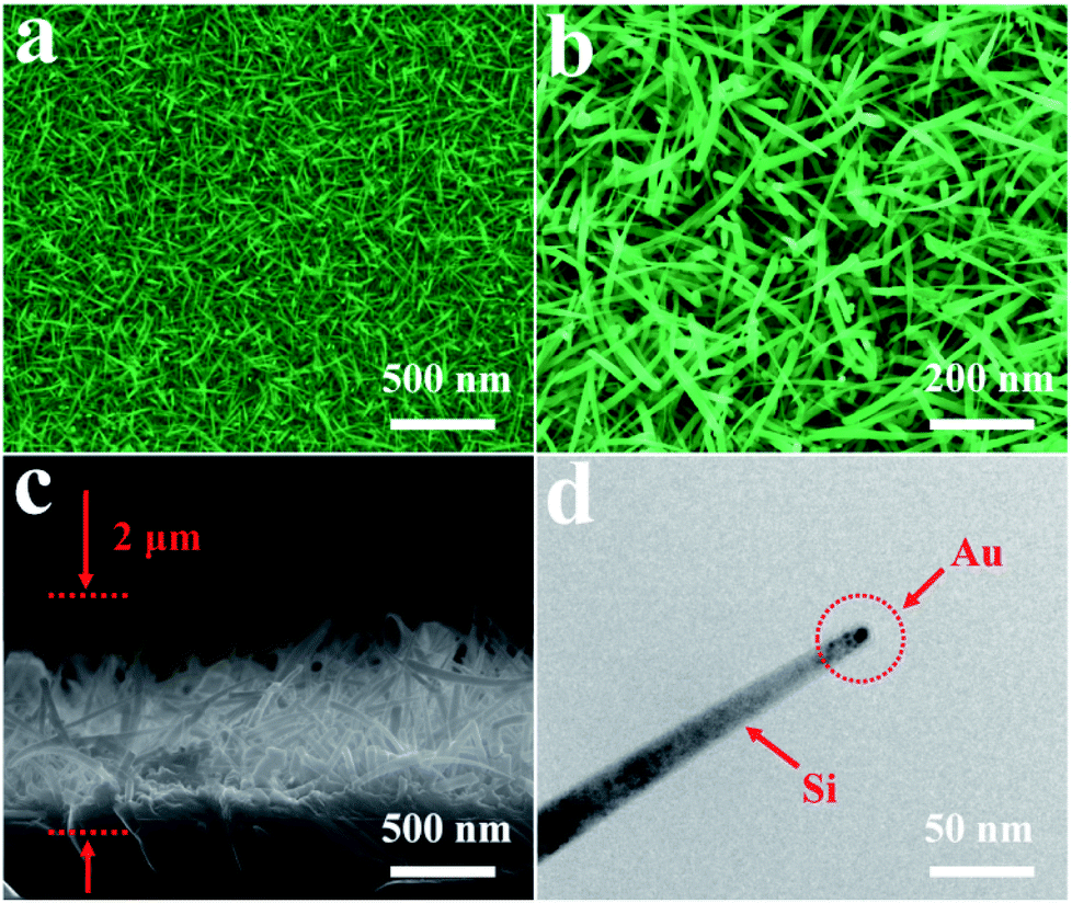 | ||
| Fig. 1 SEM and TEM images of 3D bionic silicon nanograss arrays grown on silicon substrates using PECVD method at different magnifications: (a) low-magnification SEM micrographs, (b) high-magnification SEM micrographs, (c) cross section SEM view, and (d) high-magnification TEM micrographs. | ||
The as-processed silicon nanograss is stored in vacuumed glass tubes to prevent any contact with air/oxygen and used for the subsequent decoration of AgNPs (by in situ chemical reduction viz. galvanic displacement). Furthermore, in Fig. 1d, further research found that the AuNPs catalysts are distributed mainly at the top of silicon nanograss and their external surface. Obviously, this is a typical vapor–liquid–solid (VLS) growth processes, which are universal pathway for the preparation of semiconductor nanomaterial via noble metal catalysts. The related growth mechanisms are investigated and shown in Fig. 2.
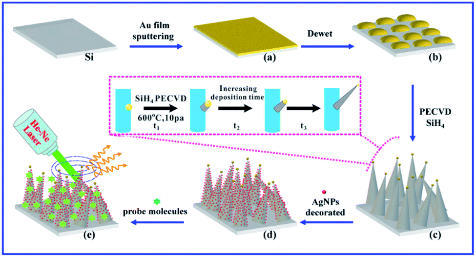 | ||
| Fig. 2 Schematic drawing of AgNPs decorated 3D bionic silicon nanograss arrays and its growth mechanism: (a) deposition of gold film, (b) dewetting evolution, (c) initial growth, (d) decoration of AgNPs, and (e) probe adsorption, SERS sensing detection. | ||
As shown in Fig. 2, high-quality 3D bionic silicon nanograss is grown on the commonly used p-type Si(100) substrates by the PECVD method, under the VLS mechanism. It is generally known that the morphology, shape, length, and diameter of the as-prepared nanograss is dependent on the type and size of catalysts during their growth. For example, Fig. 2a represents the catalyst layer of gold film deposited on the surface of silicon substrate. Usually, the gold layer is prepared by magnetron sputtering or ion sputtering, and the optimum thickness of the gold layer is found to be 5–10 nm. Then, a mild annealing experiment had been carried out under vacuum (0.1–10 mbar) in the 400–600 °C temperature range. After annealing under vacuum, which led to gold catalyst layer changes in both the morphology and component. Owing to the dewetting effect, the gold layer gradually cracked and turned into catalyst islands. It is a major step in the growth process of silicon nanograss arrays, which transformed the metal catalyst thin films into nanosize islands (Fig. 2b). During this process, the single-component catalyst nanoislands became a double-component catalyst alloy droplets (viz. gold–silicon alloys catalysts).
Many investigations indicate that the silicon comes from thermolysis of Si(100) substrates.30 Besides, small solid gold nanoparticles also catalyse the decomposition of the vaporous silane precursor, forming a liquid silicon–metal alloy. The corresponding morphology characters and component analysis of catalyst nanoislands were also investigated in our previous research. In the VLS mechanism, as more of silane precursor is added to the system, crystalline silicon nanograss arrays are excreted from the alloy due to oversaturation (Fig. 2c). Based on this mechanism, the diameter and length of the silicon nanograss arrays are directly correlated to the size of catalytic alloy droplets.
In our experimental conditions, the droplets on the tip of the silicon nanograss arrays are gradually exhausted due to thermal evaporation, plasma etching, and linear loss into the sidewall spreading, then the needle-like silicon nanograss gradually grow (Fig. 2c – inset, Fig. S2 in ESI†). The gold nanoparticles from the catalyst droplets wet the nanowires sidewalls, eventually consuming the droplets. The changeable size and shrinking droplets would directly affect the morphology of as-growth silicon nanograss arrays. That is to say, the shrinkage of silicon–gold catalyst droplets leads to gradual tapering nanograss arrays taking place (Fig. 2d).
2.2 Silver nanoparticles decorated silicon nanograss arrays and its characterization
The previous researches indicate that silver nanoparticles exhibited greater advantages in comparison to gold and copper nanoparticles owing to their stronger plasmonic ability, and can be more applicable to large-scale production.31 We herein report a facile method for the fabrication of the novel SERS substrates based on 3D bionic silicon nanograss arrays decorated with silver nanoparticles by a simple green in situ galvanic displacement and their application for the detection of ultra-low concentration of different analytes (Fig. 2d and e).As we all know that the as-prepared silicon nanograss arrays usually have an oxide outer-layer due to the oxidation process of during or after their growth. However, when the silicon nanograss arrays are immersed into hydrofluoric acid solution (5%, mass fraction), the outer oxide layer can be easily removed, and Si–H bonds (SiHx) forms on their outer surfaces. The hydrogen-terminated silicon nanograss arrays (H-SiNGAs) is a kind of moderate in situ reducing reagent, which can fast direct reduce silver ions (Ag+) to elemental silver (Ag) at room temperature in aqueous solution. Then the HF-treated silicon nanograss (SiHx) is reoxidized to SiOx surface and dissolves into the water, which exists in the form of Si(OH)4. In this process, the outer surface SiHx (x = 1–3) species are consumed quickly, which may facilitate the total redox reaction. Many studies show that hydrogen-terminated silicon nanostructures possess mild reduction properties and can be considered as the main reducing source for the decoration of noble metal nanoparticles.32 Although a plausible reaction mechanism can be deduced from the corresponding reaction products, the actual reaction between hydrogen-terminated silicon nanograss arrays and silver ions in aqueous solution is still a complex surface electrochemistry process.
Detailed information about the surface electronic structure of the obtained AgNPs/silicon nanograss arrays are investigated by X-ray photoelectron spectroscopy (XPS) with an X-ray Al-Kα source in Fig. 3a. Fig. 3b records the evolution of the Si 2p electronic state. In the Si 2p region of the as-prepared AgNPs/silicon nanograss arrays, there is an intense peak (99.38 eV) at ∼4.2 eV above the binding energy of the Si 2p (a broad peak centered at 103.68 eV). It has been established that surface Si can be readily oxidized by electronegative elements through several oxidation states, and the binding energy increase associated with a unit increase in oxidation state (Si–O bond) is ∼0.68 eV. In Fig. 3b, the intense peak is thus attributed to SiO2 on the outer layer of the 3D bionic silicon nanograss arrays. In addition, there is a broad peak centered at 103.68 eV, which is the O2s peak of oxygen in SiO2. Fig. 3c shows the XPS spectra of Ag 3d of the AgNPs. The binding energies of Ag 3d5/2 and Ag 3d3/2 are detected at 368 and 374 eV, respectively, which are well consistent with those of Ag metal, confirming that they are Ag nanoparticles on the surface of silicon nanograss arrays. The XRD pattern (Fig. 3d) demonstrates that the products have a high degree of crystallization. The main peaks of AgNPs are located at 2θ of 38.3°, 44.6°, 64.3° and 77.7°, corresponding to (111), (200), (220), and (311) planes, respectively. The results of XRD have also exhibited the nature of Ag(0), which strongly indicates that the AgNPs have been successfully modified.
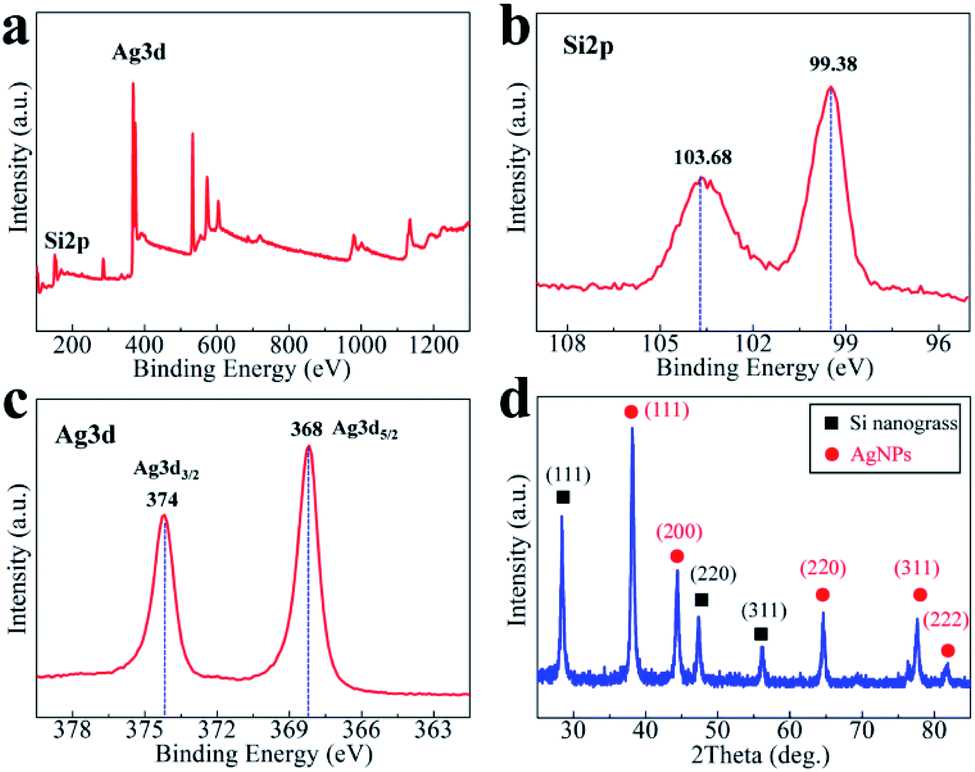 | ||
| Fig. 3 XPS spectra and XRD pattern of the as-prepared AgNPs decorated 3D bionic silicon nanograss arrays: (a) XPS survey spectrum, (b) Si 2p, (c) Ag 3d, and (d) XRD analysis. | ||
In addition, the HAADF STEM image with corresponding elemental maps results are shown in Fig. 4 (10−4 M AgNO3 aqueous solution treated silicon nanograss arrays), which also shows that they are Ag nanoparticles on the surface of 3D bionic silicon nanograss arrays. Previous research indicates that the surface morphology as well as the average size of the noble metal nanoparticles is the most significant factors in constructing ultrasensitive SERS substrates.33 By choosing and controlling the available reaction parameters, we can improve the enhancement efficiency and obtain a reliable ultrasensitive SERS substrates. Generally, it is achieved by rationally tuning the experimental parameters including the reaction time, reaction temperature, and precursor concentration.
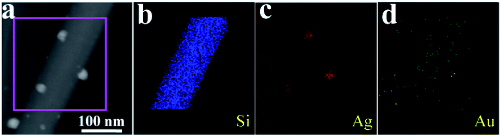 | ||
| Fig. 4 (a) HAADF STEM image and corresponding elemental mapping images for (b) Si, (c) Ag, and (d) Au are presented in panels respectively. The gold originated from catalyst residue. | ||
The effects of reaction time on the as-prepared substrate structures, morphologies, and SERS enhancement performances are investigated and shown in Fig. 5. The initial concentration of silver nitrate is up to 0.1 mM, the size evolution of silver nanoparticles is a time-dependent process. The morphology of AgNPs decorated silicon nanograss differs in different reaction time.
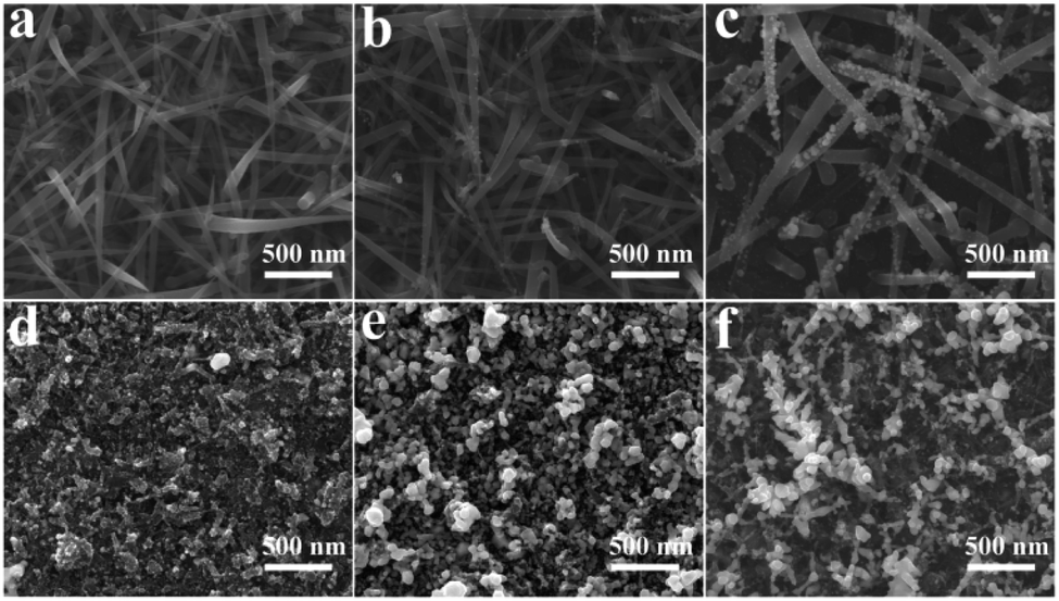 | ||
| Fig. 5 SEM images of AgNPs decorated 3D bionic silicon nanograss arrays in different reaction time: (a) 30 s, (b) 1 min, (c) 2 min, (d) 5 min, (e) 8 min, and (f) 10 min. | ||
It is obvious that the average diameter and density of AgNPs increases gradually through the different growing stages (in 2 min, Fig. 5a–c, by increasing the reaction time), and significant difference is found between these stages.
The overall result reveals that AgNPs begin to form in one minute, and nanoparticles begin to merge and coalesce with neighbouring nanowires to form composite SERS substrate in the first two minutes. However, with further extension of the reaction time, various continuous silver membrane and irregular silver nanoparticles form on the surface of the 3D bionic silicon nanograss arrays owing to the excessive aggregation nanoparticles (Fig. 5d and e). Obviously, the small Ag seeds synthesized in the early stage which act as growth seeds of the Ag plates and Ag dendrites (Fig. 5f) by further prolonging the reaction time which will lead to a decreasing SERS intensity. Some big Ag plates (Fig. 5d), Ag particles (Fig. 5e) and Ag dendrites (Fig. 5f) are formed subsequently on the silicon substrate by the accumulation of time cycles, which also disturb the displacement of AgNPs. Based on the above studies, a optimal comprehensive reaction period (2 min) of silver decoration is summarized.
Besides the reaction time, the decoration of AgNPs could also be tuned by different initial AgNO3 concentrations in the galvanic displacement reaction process. Fig. 6 shows the size evolution of AgNPs coated silicon nanograss arrays by increasing the AgNO3 concentrations. It is observed that for all six silver ion concentrations, the average size of AgNPs is formed differently on the surface of silicon nanograss. The size and number of AgNPs increases with increasing concentrations of Ag+ (from 10−6 M to 10−3 M, Fig. 6a–d), while a higher Ag+ concentration will cause irregular AgNPs (Fig. 6e) and Ag dendrites (Fig. 6f).
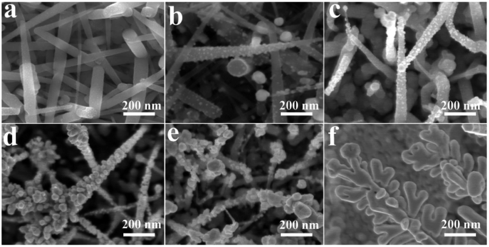 | ||
| Fig. 6 SEM images of AgNPs decorated 3D bionic silicon nanograss arrays in different initial AgNO3 concentrations: (a) 10−6 M, (b) 10−5 M, (c) 10−4 M, (d) 10−3 M, (e) 10−2 M, and (f) 10−1 M. | ||
A rough statistical results display that the average sizes of AgNPs are about 5, 10, 15 and 40 nm for 10−6 M, 10−5 M, 10−4 M and 10−3 M concentration, respectively. Based on the different average size of AgNPs, which will cause much closer gap distance. Researches show that those 3D bionic silicon nanograss arrays SERS substrates have different effectiveness in their SERS detection process.
2.3 SERS detection of R6G dye
In order to understand the relationship between SERS properties and average size of AgNPs, these six AgNPs decorated 3D bionic silicon nanograss arrays SERS substrates treated in different initial AgNO3 concentrations (from 10−1 M to 10−6 M) are evaluated by detecting the Raman spectra of the same concentration R6G. By immersing the different AgNPs size substrates into same concentration R6G aqueous solution for 3 h, a sufficient coverage of monolayer is achieved on AgNPs surface. Then the excessive molecules adsorbed on substrates are rinsed in deionized water twice and dried in N2 before acquiring the SERS spectra. The AgNPs/needle-like silicon nanograss arrays substrates prepared at different AgNO3 concentrations provide the similar R6G Raman spectra, except the intensity of main characteristic bands in Fig. 7a. The wave number from 550 to 1700 cm−1, the prominent Raman characteristic bands of R6G at 1180, 1310, 1357, 1507, 1570 and 1650 cm−1 are all observed clearly in all of these substrates which agreed well with previously literature data. The peak at 1180 cm−1 is associated with C–C in-plane bend modes, and the signals at 1310, 1357,1507, 1570 and 1650 cm−1 (between 1300 and 1700 cm−1) are due to the symmetric in-plane C–C stretching vibrations of R6G.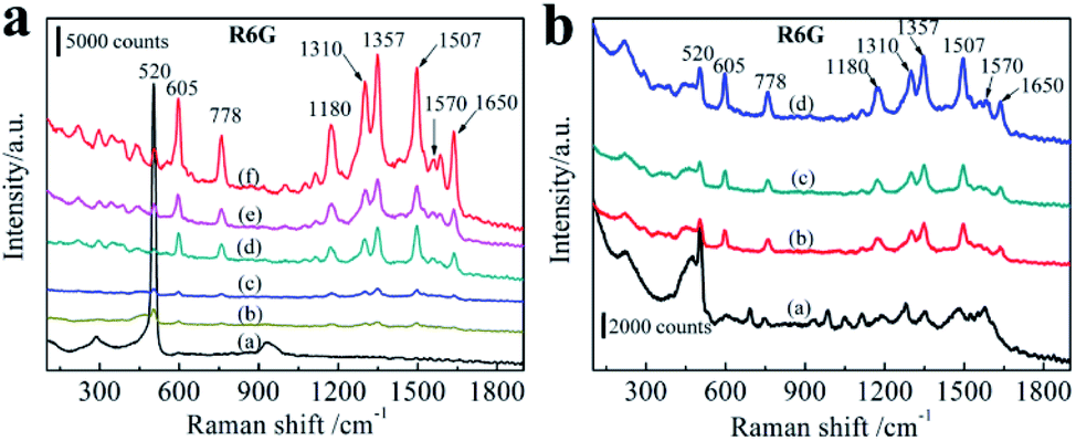 | ||
| Fig. 7 (a) 3D bionic silicon nanograss arrays treated in different AgNO3 concentration and their corresponding SERS spectra of R6G: curve (b) 10−1 M, curve (c) 10−5 M, curve (d) 10−4 M, curve (e) 10−2 M, curve (f) 10−3 M, and curve (a) 0 M; (b) SERS spectra of R6G (incident power was 3.4 mW, data acquisition time was 10 s) at different concentration: curve (a) 10−13 M, curve (b) 10−11 M, curve (c) 10−10 M, and curve (d) 10−9 M. | ||
Fig. 7a also shows that different initial AgNO3 concentration leads to different AgNPs size on the 3D bionic silicon nanograss arrays, which also exhibited different SERS spectra. In the present case, the major source of hot spots originates from the morphology of the aggregate AgNPs. In Fig. 7a, with increasing of initial AgNO3 concentrations (curve c, d, and f), the AgNPs grow larger and aggregated, the SERS intensity also increases gradually. With further extension of initial AgNO3 concentrations (curve e, b), a continuous AgNPs membrane and Ag dendrites form on the surface of 3D bionic silicon nanograss arrays due to the excessive aggregation of AgNPs on the surface, the SERS intensity begin to decrease evidently.
Curve f exhibits the strongest Raman spectra, whereas curve b and curve c provides the minimum SERS spectrum compared with the pure 3D bionic silicon nanograss arrays (curve a). We can infer that a low density and a tiny size of AgNPs (SEM Fig. 6a) prepared at lower AgNO3 concentration (10−5 M) which lead to SERS intensity decrease evidently. The same question occurs in curve b, the decreasing SERS spectrum which due to the forming of Ag dendrites (SEM Fig. 6f) at higher AgNO3 concentration (10−1 M). Once the Ag dendrites grow together on the surface of 3D substrate, the Raman enhancement disappears obviously. Curve d and curve e shows secondary Raman spectra attribute to the particle coverage density of AgNPs. Experiments indicate that a proper Ag+ concentration creates a reasonable particle coverage density and size of AgNPs on the 3D bionic silicon nanograss arrays.
The maximum SERS spectrum is shown on the curve f, SEM image shows that the substrate uniform AgNPs and close distance. A rough statistics shows the diameter is 40 nm and the gap distance is ∼9.2 nm. 10−3 M AgNO3 concentration creates an optimal size and gap distance of AgNPs on the needle-like 3D bionic silicon nanograss arrays. As the growth of diameter of AgNPs, the AgNPs begin to aggregate with narrow gaps between each other.
Fig. 7b shows the SERS spectra of R6G with a concentration gradients ranging from 10−9 down to 10−13 M. Prominent Raman spectra can be readily identified from concentration 10−13 M and above. The Raman intensity of peak at 1357 cm−1 decreases slowly with decreasing concentration of R6G, and is clearly observable as low as 10−13 M. Our experiment results indicate that the 3D bionic silicon nanograss arrays SERS substrate exhibits a lower detection limit (0.1 pM) and prominent SERS signal enhancement effect.
Furthermore, Raman enhancement factor (EF) can be estimated from the experiments (see ESI,† the five main Raman bands at 614, 776, 1360, 1507 and 1570 cm−1 are selected to calculate the average analytical enhancement factor (AEF)). On the basis of calculations, the AEF value of the AgNPs decorated 3D bionic silicon nanograss arrays substrate is estimated to 3.3 × 10⁷ (several possible factors are located at ESI†).
2.4 Practical analysis of Sudan I in environmental water
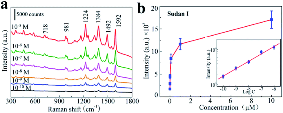
Sudan I may be one of the most notorious industrial dyes that was implicated in hot chilli powder and the chilli products, because it have a toxic effect after oral intake on the body and can lead to cause cancer in healthy adults.34–36 Many countries are making rules to detect and fight Sudan I food pollution. Sensitive detection and quantification of Sudan I dye can play important roles in food supervision and inspection. In this regard, by using a highly sensitive and reproducible SERS substrates coupled with Raman spectrometer can provides a quick qualitative and quantitative analysis with easy sample preparation. In order to investigate whether our 3D bionic silicon nanograss arrays SERS substrate is highly sensitive for Sudan I detection or not, we prepare Sudan I aqueous solutions with different concentrations from 10−5 to 10−10 M and introduce them to the nanograss arrays for SERS detection.Fig. 8a shows the representative SERS spectra of 3D bionic silicon nanograss arrays under different Sudan I concentrations and the Raman spectral intensities are decreased by diluting the Sudan I aqueous solutions. Obviously, the SERS spectra of all six Sudan I are consistent with their corresponding Raman spectra and contain all major characteristic peaks (see Table S1 in ESI†). A typical characteristic peak of Sudan I is clearly observed in each spectrum at 1592 cm−1 which is assigned to the stretching vibration of the benzene ring.37,38 These distinct characteristic peaks (at 1592 cm−1) are observed even when the Sudan I concentration was down to 10−10 M, demonstrating the high sensitivity of the as-prepared 3D silicon nanograss arrays. More importantly, it is much lower than the general default MRLs in many countries.39 Such a low limit of detection enables the as-fabricated silicon nanograss arrays SERS substrates could be utilized toward the goal of trace analysis of illegal additive residues.40 The increasing trend of SERS intensity with Sudan I concentration is further summarized in Fig. 8b for quantitative Sudan I sensing. And the intense SERS peak at 1592 cm−1 in the spectra has been used as a calibration band. A gradual increase in SERS intensity is observed as the Sudan I concentration increasing. Above 10−5 M, a step response is observed in signal intensity, indicating a stronger response to high concentration of Sudan I.
 | ||
| Fig. 8 (a) SERS spectra of Sudan I (incident power was 3.4 mW, data acquisition time was 10 s) at different concentrations; R6G Raman spectra; (b) plot of the peak intensity at 1592 cm−1 as a function of Sudan I concentration (inset represents the linear relationship from 10−10 M to 10−6 M). | ||
The calibration curve in the concentration ranging from 10−10 to 10−6 M is shown in Fig. 8b (inset). The linear equation is determined as log![[thin space (1/6-em)]](https://www.rsc.org/images/entities/char_2009.gif) I1592 = (0.2113 ± 0.1577)logC + (5.3580 ± 0.1287), (10−10 < C < 10−6) with the correlation coefficient R2 = 0.992, where I1592 is the SERS intensity and C is the concentration of Sudan I dye. Based on these studies, the linear equation could provide an opening for fast ultra-sensitive analysis of trace Sudan I in environmental water or illegal additive-contaminated products, which has the potential for a practical application. Moreover, the quantification of ultra-trace Sudan I residual in environment water is successfully carried out with the recovery of 89.4% to 112.0% (Table S2, ESI†). The stability and durability of the prepared substrates are investigated in Fig. S3 (ESI†), and exhibited a good stability in 15 days, a 19% decrement after one month. These results confirm the practical application of our 3D bionic SERS substrate with high accuracy and reliability.
I1592 = (0.2113 ± 0.1577)logC + (5.3580 ± 0.1287), (10−10 < C < 10−6) with the correlation coefficient R2 = 0.992, where I1592 is the SERS intensity and C is the concentration of Sudan I dye. Based on these studies, the linear equation could provide an opening for fast ultra-sensitive analysis of trace Sudan I in environmental water or illegal additive-contaminated products, which has the potential for a practical application. Moreover, the quantification of ultra-trace Sudan I residual in environment water is successfully carried out with the recovery of 89.4% to 112.0% (Table S2, ESI†). The stability and durability of the prepared substrates are investigated in Fig. S3 (ESI†), and exhibited a good stability in 15 days, a 19% decrement after one month. These results confirm the practical application of our 3D bionic SERS substrate with high accuracy and reliability.
3. Experimental
3.1 Chemical reagents
Silver nitrate (AgNO3) was purchased from Xi'an Dayu Chemicals Industry; hydrofluoric acid (HF) was purchased from Dongjiang Chemicals Company; silicon (Si) wafers were purchased from Luoyang Single Crystal Silicon Company; silane (SiH4) was purchased from Nanjing Specialty Gas Company; Rhodamine 6G (R6G), Sudan I was purchased from J&K Chemical in Beijing. All chemicals were used as received, without further purification. Milli-Q water (>18.0 MΩ cm) was used throughout the experiments. The environmental water comes from the eastern lake of Xi'an.3.2 Preparation of 3D bionic silicon nanograss arrays
The 3D bionic silicon nanograss arrays used in this work were prepared by plasma enhanced chemical vapor deposition (PECVD) method, because the PECVD technology can better meet the deposition requirements of high-efficiency, low-cost, large-scale, and homogeneous distribution. The growth of silicon nanograss was carried out in PECVD chamber based a gold-catalyzed vapor–liquid–solid (VLS) growth mechanism. The detailed experimental procedure for the preparation of silicon nanograss involved the following steps: first, the precut silicon (100) chips (5 cm × 5 cm) were ultrasonically cleaned sequentially in alcohol, acetone, and deionized (DI) water each for 10 min, respectively, and then dried with nitrogen blow before they were placed into the vacuum chamber. Second, a thin gold layer of 10 nm was magnetron sputtered (or ion sputtering) on top of silicon substrates. Then, the substrates were loaded into the PECVD reactor, where alloy droplets were formed by vacuum annealing at a temperature of 800 °C. Finally, the growths of needle-like Si nanowires were performed for 1 h in a low pressure PECVD system by using silane as precursor. The reaction temperature can be selected from 450 to 800 °C, the base pressure of the vacuum chamber was 4.0 × 10⁻⁴ Pa, the silane (40 sccm, 10% in hydrogen) pressure was 250 mTorr when sputtering, and the radio frequency power was 30 mW cm−2.3.3 AgNPs decorated 3D bionic silicon nanograss arrays and corresponding characterization
In order to obtain the H-terminal silicon nanograss arrays, the as-prepared 3D bionic silicon nanograss arrays substrates were immerged into a 5% HF aqueous solution for 2 min. Then, the HF-etched silicon nanograss were rinsed with deionized water twice and immediately dipped into aqueous solutions of silver(I) nitrate shaking slightly for one minute. After the galvanic displacement reaction, the treated silicon nanograss were rinsed in deionized water and dried immediately by nitrogen blow and transferred into a vacuum chamber for further measurements.The structure and morphology of the obtained silicon nanograss arrays were characterized X-Ray Diffraction (XRD, Bruker D8 ADVANCE), Scanning Electron Microscopy (SEM, Hitachi S4800) and Transmission Electron Microscopy (TEM, JEM-2100F). The surface state of the as-synthesized SERS substrates were analyzed by PHI-5400 X-ray photoelectron spectrometer (Perkin Elmer Inc) using an X-ray Al-Kα source as a probe. An electron flood gun was used for all measurements to compensate charging, and the final spectra were calibrated to the adventitious carbon C1s peak at 284.6 eV.
3.4 SERS measurements
Using the as-prepared AgNPs decorated 3D bionic silicon nanograss arrays as SERS-active substrates, and a UNISOKU-TII (Tokyo Instruments) laser confocal Raman spectrometer was used to carry out the SERS measurements. R6G was chosen as a model analyte to investigate the performance of the 3D SERS substrate because it is extensively studied and well characterized by Raman spectroscopy. The SERS measurements were performed by dipped the substrates into 5 mL R6G solution of different concentrations (from 10−6 M to 10−14 M) for 3 hours. He–Ne laser of 632.8 nm at a spectral resolution of 1 cm−1 and a spot size of 1 μm was used for excitation. The laser power on the specimens was measured at 3.4 mW. The recorded spectra were raw data without any background subtraction or processing.4. Conclusions
In this study, a AgNPs decorated 3D bionic silicon nanograss arrays SERS substrate was successfully fabricated, using the shrinkage of Au catalyst droplet in VLS growth and subsequent galvanic displacement decoration. The clean surfaces, high-density hot spots, and significant Raman signal amplification were obtained by adjustable reaction time and silver ion concentration. The optimal AgNPs decorated 3D bionic silicon nanograss arrays were able to detect R6G down to 0.1 pM, and the analytical enhancement factor (AEF) was estimated to be 3.3 × 10⁷, which is obviously superior to that of pure silicon or silver nanostructures. Importantly, a remarkably low concentration of Sudan I down to 0.1 nM (much lower than those traditional analytical approaches) can readily be discriminated via the developed SERS substrates. Besides the SERS sensing, the substrates obtained in this study might be widely applied in many different fields, such as medical diagnosis, environment supervision, and catalytic conversion.Author contributions
Jian Huang and Li Wang are considered co-first authors, both authors contributed equally to this work. All authors declare no competing financial interests.Conflicts of interest
There are no conflicts to declare.Acknowledgements
This research was funded by the Natural Science Basic Research Program of Shaanxi (No. 2019JQ-490), Scientific Research Program Funded by Shaanxi Provincial Education Department (No. 21JK0835), and the Innovation and Practice Ability Training Project for Postgraduates of Xi'an Shiyou University (No. YCS20211022).Notes and references
- X. Yao, S. Jiang, S. Luo, B.-W. Liu, T.-X. Huang, S. Hu, J. Zhu, X. Wang and B. Ren, ACS Appl. Mater. Interfaces, 2020, 12, 36505–36512 CrossRef CAS.
- Y. Wang, B. Yan and L. Chen, Chem. Rev., 2013, 113, 1391–1423 CrossRef CAS PubMed.
- J. Li, L. Chen, T. Lou and Y. Wang, ACS Appl. Mater. Interfaces, 2011, 3, 3936–3941 CrossRef CAS PubMed.
- R. Mei, Y. Wang and Q. Yu, et al., ACS Appl. Mater. Interfaces, 2020, 12, 2059–2066 CrossRef CAS.
- F. Xu, M. Xuan, Z. Ben, W. Shang and G. Ma, Rev. Anal. Chem., 2021, 40, 75–92 CrossRef CAS.
- P. Wang, Y. Sun, X. Li, L. Wang, Y. Xu and G. Li, Molecules, 2021, 26, 209 CrossRef CAS.
- M. Muhammad and Q. Huang, Talanta, 2021, 227, 122188 CrossRef CAS PubMed.
- A. Kapara, V. Brunton, D. Graham and K. Faulds, Chem. Sci., 2020, 11, 5819–5829 RSC.
- G. Pavliuk, D. Pavlov, E. Mitsai, O. Vitrik, A. Mironenko, A. Zakharenko, S. A. Kulinich, S. Juodkazis, S. Bratskaya, A. Zhizhchenko and A. Kuchmizhak, Nanomaterials, 2020, 10, 49 CrossRef CAS PubMed.
- X. Jing, L. Chang, L. Shi, X. Liu, Y. Zhao and W. Zhang, ACS Appl. Bio Mater., 2020, 3, 2385–2391 CrossRef CAS.
- L. G. Quagliano, B. Jusserand and D. J. Orani, Raman Spectrosc., 1998, 29, 721–724 CrossRef CAS.
- T. Wang, Z. Zhang, F. Liao, Q. Cai, Y. Li, S.-T. Lee and M. Shao, Sci. Rep., 2014, 4, 1–8 Search PubMed.
- A. Fularz, S. Almohammed and J. H. Rice, ACS Appl. Nano Mater., 2020, 3, 1666–1673 CrossRef CAS.
- M. Jue, C. G. Pack, S. Oh, B. Paulson, K. Lee and J. K. Kim, Materials, 2020, 13, 5321 CrossRef CAS.
- P. Zhang, G. Liu, W. Xu, L. Meng, X. Wang, L. Shang, Y. Xiong, Q. Luo and S. Feng, ACS Omega, 2020, 5, 31730–31737 CrossRef CAS.
- J. Huang, Y. Sun, S. Huang, K. Yu, Q. Zhao, F. Peng, H. Yu, H. Wang and J. Yang, J. Mater. Chem., 2011, 21, 17930–17937 RSC.
- L. Sun, J. He, S. An, J. Zhang and D. Ren, J. Mol. Struct., 2013, 1046, 74–81 CrossRef CAS.
- S. Zhu, C. Fan, J. Wang, J. He, E. Liang and M. Chao, J. Colloid Interface Sci., 2015, 438, 116–121 CrossRef CAS.
- M. Muniz-Miranda, C. Gellini, E. Giorgetti and G. Margheri, J. Colloid Interface Sci., 2017, 489, 100–105 CrossRef CAS.
- J. Cai, J. Huang, M. Ge, J. Iocozzia, Z. Lin, K. Zhang and Y. Lai, Small, 2017, 13, 1604240 CrossRef.
- S. Park, P. Yang, P. Corredor and M. J. Weaver, J. Am. Chem. Soc., 2002, 124, 2428–2429 CrossRef CAS.
- T. Hinamoto, S. Hotta, H. Sugimoto and M. Fujii, Nano Lett., 2020, 20, 7737–7743 CrossRef CAS.
- X. Wan, X. Chen, S. Yang, W. Ma, S. Li and K. Wei, Mater. Lett., 2020, 268, 127616 CrossRef CAS.
- S. Kuhn, P. Asenbaum, A. Kosloff, M. Sclafani, B. A. Stickler, S. Nimmrichter, K. Hornberger, O. Cheshnovsky, F. Patolsky and M. Arndt, Nano Lett., 2015, 15, 5604–5608 CrossRef CAS.
- M.-L. Zhang, X. Fan, H.-W. Zhou, M.-W. Shao, J. A. Zapien, N.-B. Wong and S.-T. Lee, J. Phys. Chem. C, 2010, 114, 1969–1975 CrossRef CAS.
- B. Reddyg G, R. Dadigala and R. Bandi, et al., RSC Adv., 2021, 11, 5139–5148 RSC.
- C. Fang, A. Agarwal, H. Ji, W. Y. Karen and L. Yobas, Nanotechnology, 2009, 20, 405604 CrossRef CAS PubMed.
- B. Hua, W. Zhang and L. Chen, et al., J. Appl. Phys., 2012, 112, 124301–124306 CrossRef.
- R. Frederiksen, G. Tutuncuoglu and F. Matteini, et al., ACS Photon., 2017, 4, 2235–2241 CrossRef CAS.
- S. Botti, R. Ciardi, R. Larciprete, A. Goldoni, L. Gregoratti, B. Kaulich and M. Kiskinova, Chem. Phys. Lett., 2003, 371, 394–400 CrossRef CAS.
- L. Wang, H. Li, J. Tian and X. Sun, ACS Appl. Mater. Interfaces, 2010, 2, 2987–2991 CrossRef CAS PubMed.
- P. M. Ryan, L. Livadaru, G. A. DiLabio and R. A. Wolkow, J. Am. Chem. Soc., 2012, 134, 12054–12063 CrossRef CAS PubMed.
- S. R. Emory, W. E. Haskins and S. Nie, J. Am. Chem. Soc., 1998, 120, 8009–8010 CrossRef CAS.
- Y. Zhao, G. Chen, Y. Du, J. Xu, S. Wu, Y. Qu and Y. Zhu, Nanoscale, 2014, 6, 13754–13760 RSC.
- C. Di Anibal, M. S. Rodriguez and L. Albertengo, Food Anal. Methods, 2014, 7, 1090–1096 CrossRef.
- Q. Shao, R. Que, M. Shao, L. Cheng and S.-T. Lee, Adv. Funct. Mater., 2012, 22, 2067–2070 CrossRef CAS.
- X. Kong, K. Squire, X. Chong and A. X. Wang, Food Control, 2017, 79, 258–265 CrossRef CAS.
- Q. Cao, X. Liu, K. Yuan, J. Yu, Q. Liu, J.-J. Delaunay and R. Che, Appl. Catal., B, 2017, 201, 607–616 CrossRef CAS.
- B. Liu, P. Zhou, X. Liu, X. Sun, H. Li and M. Lin, Food Bioprocess Technol., 2013, 6, 710–718 CrossRef CAS.
- X. Lu, W. Liu, C. Chen, G. Jiang, X. Hu, H. Zhang and M. Zhong, Laser Technol., 2021, 139, 106969 CrossRef.
Footnotes |
| † Electronic supplementary information (ESI) available. See DOI: 10.1039/d1ra04874k |
| ‡ These two authors have made an equal contribution to this work and hold joint first authorship. |
| This journal is © The Royal Society of Chemistry 2021 |