
 Open Access Article
 This Open Access Article is licensed under a Creative Commons Attribution-Non Commercial 3.0 Unported Licence
High responsivity and high speed InGaN-based blue-light photodetectors on Si substrates
Jixing Chaiab,
Deqi Kongab,
Sheng Chenab,
Liang Chenab,
Wengliang Wang *abc and
Guoqiang Li*abc
*abc and
Guoqiang Li*abc
aState Key Laboratory of Luminescent Materials and Devices, South China University of Technology, Guangzhou 510640, China. E-mail: wenliangwang@scut.edu.cn; msgli@scut.edu.cn
bSchool of Material Science and Engineering, South China University of Technology, Guangzhou 510640, China
cGuangdong Choicore Optoelectronics Co. Ltd., Heyuan 517003, China
First published on 19th July 2021
Abstract
Due to the adjustable band gap, the excellent radiation stability, and the high electron mobility of InGaN, the InGaN-based blue-light photodetectors (PDs) show great potential in visible light communication (VLC) systems. However, the applications of InGaN-based blue-light PDs in VLC systems are limited by the poor performance caused by the poor crystalline quality of InGaN materials. Herein, we report on the fabrication of high responsivity and high response speed InGaN-based metal–semiconductor metal (MSM) blue-light PDs using high-quality InGaN epitaxial films grown on Si substrates by the combination of low-temperature pulsed laser deposition (LT-PLD) and high-temperature metal organic chemical deposition (HT-MOCVD). The technology can not only suppress the interfacial reactions between films and substrates by LT-PLD growth, but also promote the lateral overgrowth of InGaN and improve the crystalline quality of InGaN-based epitaxial films by HT-MOCVD growth. Based on the high-quality InGaN-based materials, high-performance InGaN-based blue-light PDs are fabricated accordingly with a high responsivity of 0.49 A W−1 and a short rise/fall response time of 1.25/1.74 ms at an applied bias of −3 V. The performance is better than the results for the InGaN-based PDs previously reported. The InGaN-based blue-light PDs shed light on the potential for VLC system applications.
1. Introduction
Due to the high-speed transfer rate, broader unlicensed spectrum, lower power consumption and strong data confidentiality, visible light communication (VLC) shows great potential for application in the fields of national economy and defense.1–3 It is known that photodetectors (PDs) play a core role in VLC hardware and determine the transmission rate and reliability of VLC systems.4–6 Therefore, PDs have attracted great attention. The traditional PDs applied in VLC systems are Si-based PDs, which have the advantages of low cost and compatibility with complementary metal oxide semiconductor technology (CMOS).7,8 However, Si-based PDs can't meet the recent demand for high signal-to-noise ratio in VLC systems owing to their wide-spectrum response characteristics.9–11InGaN can achieve wavelength-selective detection through controlling In content in InGaN alloy, and therefore InGaN-based PDs are the optimal candidates for VLC system.12–14 InGaN-based PDs are usually prepared based on sapphire substrates. To date, although considerable progresses have been achieved, the reliability and applicability of InGaN-based PDs on sapphire substrates is poor mainly caused by the small thermal conductivity of substrates. To circumvent the issues, InGaN epitaxial films grown on high thermal conductivity Si substrates would be an effective approach.15–17 Furthermore, InGaN-based PDs on Si substrates have great potential in VLC applications owing to the compatibility with Si-based CMOS process as well as the low cost and available to large size of Si substrates. However, it is difficult to grow the high-quality InGaN epitaxial films on Si substrates owing to the large lattice and thermal mismatches between the epitaxial films and the substrates.18,19
In this work, we fabricate high responsivity and high response speed InGaN-based metal–semiconductor metal (MSM) blue-light PDs based on the high-quality the InGaN-based epitaxial films grown on Si substrates by the combination of low-temperature pulsed laser deposition (LT-PLD) and high-temperature metal organic chemical deposition (HT-MOCVD) technologies. On the one hand, the LT-PLD can provide highly energy for precursors to migrate on substrate surfaces at LT, which can effectively suppress the interfacial reactions between films and substrates. On the other hand, the high-quality buffer layer prepared with HT-MOCVD can promote the lateral overgrowth of InGaN-based epitaxial films, which can enhance the annihilation of dislocations and thereby improve the crystalline quality of InGaN-based epitaxial films. These two aspects ensure the growth of high-quality and crack-free epitaxial films for the fabrication of InGaN-based blue-light PDs devices with a high responsivity of 0.49 A W−1 @ 425 nm and shorter rise/fall response time of 1.25/1.74 ms at an applied bias of −3 V.
2. Experimental procedures
The InGaN epitaxial films were grown on 4 inch Si substrate. The epitaxial structures of the InGaN-based blue-light PDs wafers of sample 1 are shown in Fig. 1(a). Firstly, the Si substrate were taken through a cleaning process with acetone, alcohol and deionized water in order to remove surface contamination. Secondly, the as-cleaned substrates were transferred into the PLD growth chamber. Subsequently, a ∼200 nm-thick AlN layer and ∼500 nm-thick AlGaN layer were grown on Si substrates by PLD with a target substrate distance of 5 cm and an optimized laser density of 3.0 J cm−2 in a 4 mTorr nitrogen plasmas atmosphere produced by a radio-frequency plasma radical generator at temperatures of 450 °C, respectively. Thirdly, the template was transferred into a MOCVD growth chamber, trimethylgallium (TMGa), trimethylindium (TMIn) and ammonia were used as the precursors for Ga and N, respectively. A ∼1 μm GaN and 100 nm InGaN epitaxial films were grown at a temperature of 1100 and 750 °C, respectively, and these were named sample 1. For comparison, AlN/AlGaN buffer layer were grown on Si substrates with MOCVD at temperatures of 1100 and 850 °C, respectively, were named sample 2. For the growth of AlN/AlGaN buffer layer, triethylgallium (TMGa), trimethylaluminum (TMAl) and ammonia were used as precursors for Ga, Al and N, respectively.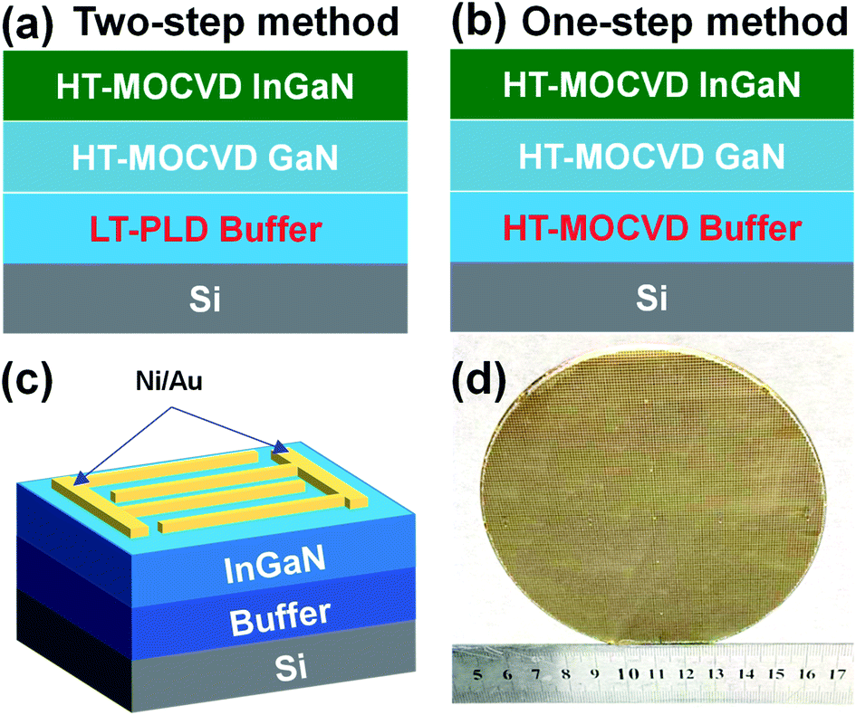 | ||
| Fig. 1 Schematic diagram of epitaxy InGaN film with different method (a) two-step method, (b) one-step method. (c) The schematic structures for the PDs. (d) Photograph of the chip on wafer. | ||
The InGaN epitaxial films of samples 1 and 2 were fabricated into MSM blue-light PDs by standard photolithography. Electron beam evaporation was adopted to deposit Ni/Au as an electrode, Fig. 1(c), and the finger length, width, and spacing for the electrode were 200, 5 and 5 mm, respectively. Afterwards, chips on wafers were obtained, Fig. 1(d). The R, dark current, and response time for these samples were studied using an optical platform with a xenon light source (150 W), an Omni-λ 300 monochromator and a Keithley 2400 electrometer.
The as-grown InGaN-based epitaxial films grown on Si substrates were characterized by high-resolution X-ray diffraction (HRXRD, Bruker, D8 X-ray diffractometer with Cu Kα1 X-ray source, l = 0.15406 nm), atomic force microscopy (AFM, Bruker Dimension Edge), optical microscopy (OM, OLYMPUS, BX51M), high-resolution transmission electron microscopy (HRTEM, FEI, TECNAI G2 S-TWIN F20), and Hall measurement (lake shore 8400).
3. Results and discussion
The optical microscopy (OM) images of samples 1 and 2 were shown in Fig. 2(a) and (b). For the sample 1, there are no cracks existing on the surface. On the contrary, there are many obvious cracks to be observed on the surface of sample 2. The results proved that the method of the combination of PLD and MOCVD can effectively reduce defects. The atomic force microscopy (AFM) images for samples 1 and 2 are shown in Fig. 2(c) and (d), it is observed that the value of root-mean-squared (RMS) roughness for sample are 3.3 and 4.2 nm, respectively. Compared with sample 1, the surface of sample 2 is relatively rough, which can be attributed to the different growth conditions. By optimizing the growth conditions of MOCVD, the lateral growth rate for InGaN is enhanced, and the coalescence of the disoriented individual islands is also promoted. These ultimately result in the smooth surfaces of InGaN epitaxial materials.20,21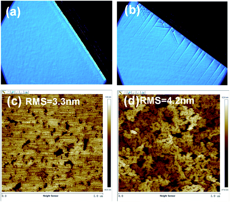 | ||
| Fig. 2 The optical microscopy images of InGaN with different method (a) sample 1, (b) sample 2. The AFM images of InGaN with different method (c) sample 1, (d) sample 2. | ||
X-ray rocking curves (XRCs) are used to measure the crystalline quality of InGaN epitaxial films. Fig. 3(a) and (b) show the typical XRCs for InGaN(0002) and InGaN(10![[1 with combining macron]](https://www.rsc.org/images/entities/char_0031_0304.gif) 2) of samples 1 and 2, respectively. We can identify that the full-width at half-maximums (FWHMs) of InGaN(0002) and InGaN(102) XRCs for sample 1 are of the average values of 276 and 313 arcsec, respectively, which are smaller than those average values for sample 2 of 314 and 352 arcsec. Based on the results mentioned above, the InGaN epitaxial films of sample 1 reveal a better crystalline quality. These differences are attributed to the different growth method, and the high-quality InGaN epitaxial films achieved can be mainly attributed to the combination of PLD and MOCVD method. PLD can supply enough energy for the migration of precursors, and thereby realize LT growth by effectively controlling the interfacial reactions between buffer and Si substrate, which enhances the crystalline quality of InGaN.20–22 To investigate the influence of the growth method on the interfacial reactions, the TEM characterization of interface between buffer and Si substrate for samples 1 and 2 is employed as shown in Fig. 3(c) and (d). For sample 1, both the clear and sharp buffer and Si substrate heterointerfaces can be identified from Fig. 3(c). However, the fuzzy buffer and Si substrate heterointerfaces could be observed for sample 2 on Fig. 3(d). Therefore, the LT-PLD could effectively suppressing the interfacial reactions between films and substrates, and provide a high-quality basic template for the high-quality InGaN epitaxial films.
2) of samples 1 and 2, respectively. We can identify that the full-width at half-maximums (FWHMs) of InGaN(0002) and InGaN(102) XRCs for sample 1 are of the average values of 276 and 313 arcsec, respectively, which are smaller than those average values for sample 2 of 314 and 352 arcsec. Based on the results mentioned above, the InGaN epitaxial films of sample 1 reveal a better crystalline quality. These differences are attributed to the different growth method, and the high-quality InGaN epitaxial films achieved can be mainly attributed to the combination of PLD and MOCVD method. PLD can supply enough energy for the migration of precursors, and thereby realize LT growth by effectively controlling the interfacial reactions between buffer and Si substrate, which enhances the crystalline quality of InGaN.20–22 To investigate the influence of the growth method on the interfacial reactions, the TEM characterization of interface between buffer and Si substrate for samples 1 and 2 is employed as shown in Fig. 3(c) and (d). For sample 1, both the clear and sharp buffer and Si substrate heterointerfaces can be identified from Fig. 3(c). However, the fuzzy buffer and Si substrate heterointerfaces could be observed for sample 2 on Fig. 3(d). Therefore, the LT-PLD could effectively suppressing the interfacial reactions between films and substrates, and provide a high-quality basic template for the high-quality InGaN epitaxial films.
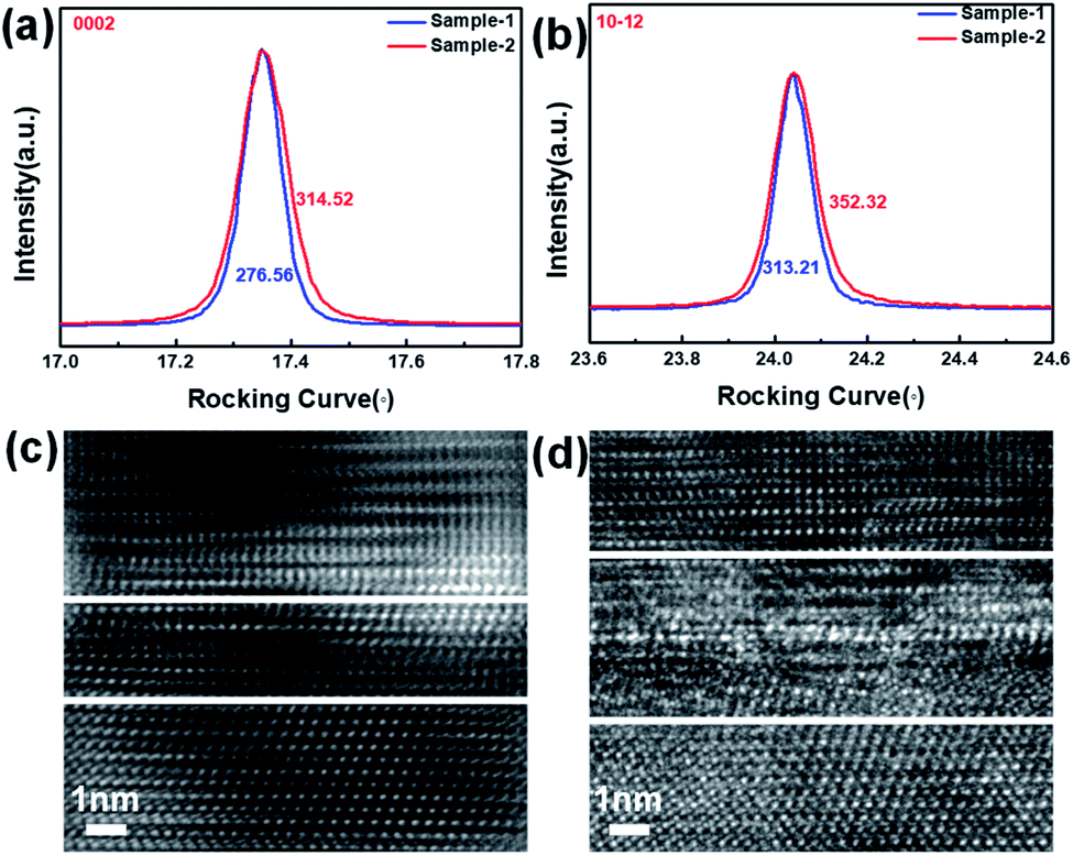 | ||
| Fig. 3 (a) InGaN(0002) and (b) InGaN(102) XRCs for sample 1 and 2. HRTEM image for (c) sample 1 and (d) sample 2. | ||
To further evaluate the electrical properties of the prepared samples, we can measure the conductive type, carrier concentration, mobility, and resistivity of semiconductors by Hall effect measurement. Details can be found in Table 1. The results indicate that sample 1 show better electrical properties than sample 2.
| Sample | Conductive type | Carrier concentration (cm−3) | Mobility (cm−3 V−1 s−1) | Resistivity (ohm cm−1) |
|---|---|---|---|---|
| Sample 1 | n | 4.1 × 10¹⁷ | 250.34 | 0.7 |
| Sample 2 | n | 2.3 × 10¹⁷ | 140.51 | 17 |
To evaluate the performance of the InGaN-based blue-light PDs, the I–V curves for sample 1-based PDs and sample 2-based PDs were characterized under dark and 430 nm light conditions, and the results are shown in Fig. 4(a). It can be found that in the dark, I for these two devices are 2.53 and 9.14 μA respectively at an applied bias of −3 V. Moreover, we can also identify the photo-to-dark current ratio from Fig. 4(a). In this case, at an applied bias of 3 V, the photo-to-dark current ratios for sample 1 and 2 based devices are 6.24 and 1.82, respectively. Fig. 4(d) shows the responsivity (R) for the sample 1 and sample 2 based blue-light PDs. It can be found that the R reaches peak values of 0.49 and 0.27 A W−1 at 425 nm for these two PDs, respectively, at an applied bias of −3 V. The R for the sample 1 based blue-light PDs is relatively high, which is ascribed to high crystalline quality and smooth surface of the InGaN epitaxial films grown by the combination of LT-PLD and HT-MOCVD. Moreover, the R reaches 0.03 and 0.02 A W−1 at 500 nm for these two PDs, respectively, at an applied bias of −3 V. The blue/500 nm rejection ratio for these devices is of 18.15 and 12.53, respectively, which indicate high spectral selectivity of the blue region. Detectivity (D* = RA1/2/(2eIdark)1/2, which A is the active area of a photodetector device, and e is the electron charge)23 is a key parameter that describes the ability of a photodetector to measure the weakest detectable signals. The D* of sample 1 and 2 based blue-light PDs is 7.81 × 10⁹ jones and 2.56 × 10⁹ jones, respectively. The D* of sample 1 based blue-light PDs is significantly higher than that of sample 2 based blue-light PDs thanks to the higher crystalline quality of InGaN in sample 1 that leads to the lower Idark.24,25
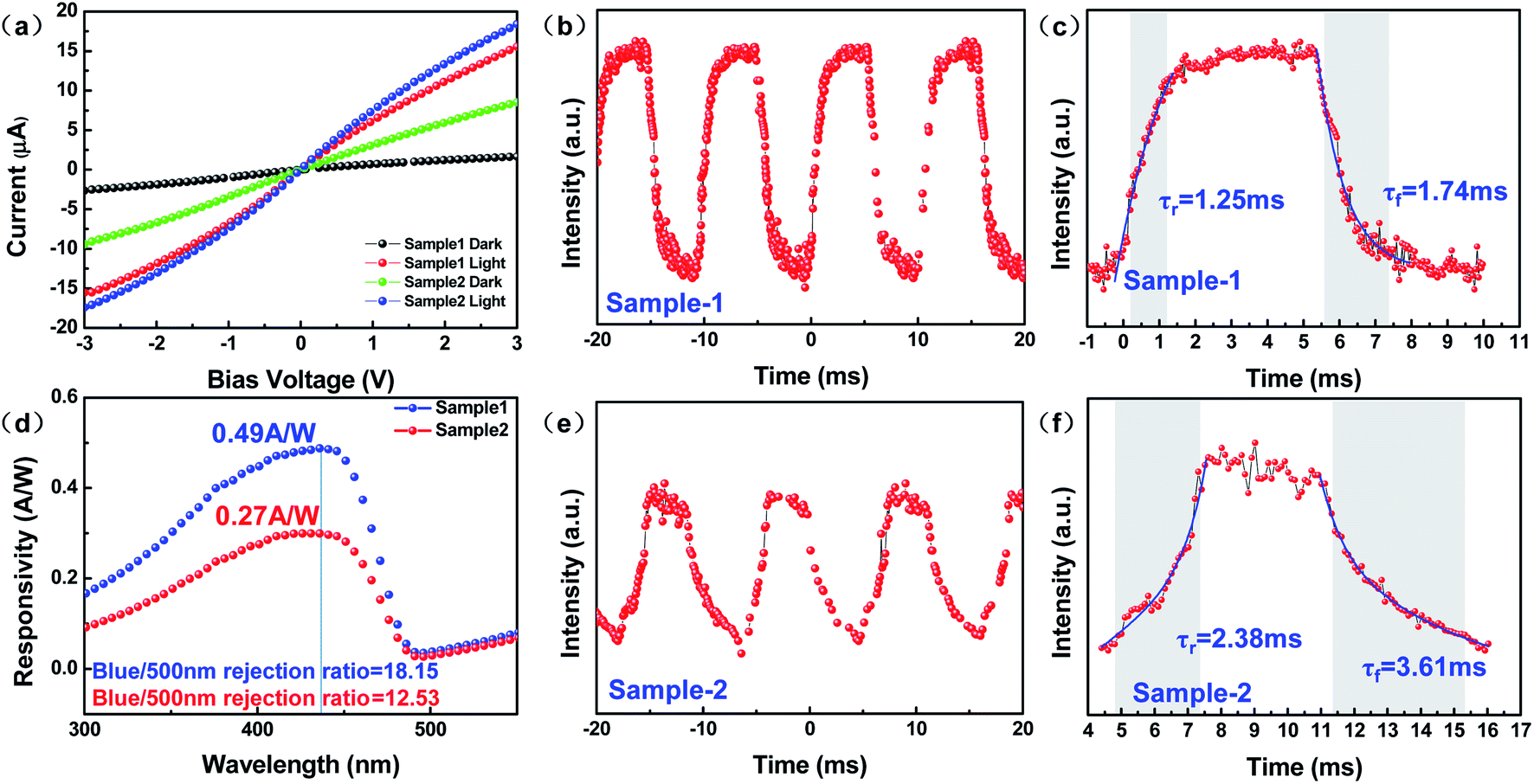 | ||
| Fig. 4 Photoelectric performance of InGaN-based blue-light photodetectors. (a) I–V characteristic curve for different photodetectors; (b, c) and (e, f) time response curve; (d) responsivity curves for different photodetectors. | ||
To measure the response speed of the fabricated blue-light PDs, the time response of the photo-current for rise time and fall time of the sample 1 based and sample 2 based blue-light PDs was carried out as shown in Fig. 4(b, c) and (e, f), respectively. The rise time and the fall time of the sample 1 based blue-light PDs were measured to be 1.25 and 1.74 ms from Fig. 4(c), respectively, while the rise time and the fall time of the sample 2 based blue-light PDs were found to be 2.38 and 3.61 ms from Fig. 4(f), respectively. Compared with the sample 1 based blue-light PDs, the rise/fall time for sample 2 based blue-light PDs is relatively long, the slow response speed of the sample 2 based blue-light PDs can be ascribed to the high dislocation density. It is well known that the carriers trapped by dislocations are in thermodynamic equilibrium, which results in the thermally assisted re-emission of captured carriers, thereby increasing the rise time.26–28 Meanwhile, the photogenerated carriers trapped by dislocation will be released to the steady-state when the light is switched off, in this case, the fall time of PDs is increased accordingly.26–28
Compared with the sample 2 based blue-light PDs, the sample 1 based blue-light PDs reveal higher R, smaller dark I, and shorter response time. Moreover, the R of the sample 1 based blue-light PDs reveals the best values among the InGaN-based PDs ever reported as listed in Table 2. The excellent properties of sample 1 based blue-light PDs are attributed to the higher crystalline quality and smoother surfaces of the InGaN epitaxial films achieved by two-step method in this work. As we all known that dislocation play the role of non-radiative center and leakage path, which can increase the leakage path and enhance the transition time for carriers.
| Device | Responsivity | τr/τf | Ref. |
|---|---|---|---|
| In0.15Ga0.85N-MSM | 0.49 A W−1 @ 3 V | 1.25/1.74 ms | This work |
| In0.15Ga0.85N-MSM | 85 mA W−1 @ 5 V | — | 29 |
| In0.17Ga0.83N-MSM | 0.22 A W−1 @ 1.5 V | — | 30 |
| In0.37Ga0.63N-MSM | 0.144 A W−1 @ 5 V | — | 31 |
| InGaN monolithic photonic chip | — | 33.9/34.7 ms | 32 |
| n-InGaN/n-Si | 0.0942 A W−1 @ 0 V | 20/33 ms | 33 |
| GaN MWA/Si | 0.47 A W−1 @ −2 V | 2/2 ms | 34 |
4. Conclusion
In summary, InGaN-based blue-light PDs with high responsivity and fast response speed have been fabricated based on high-quality InGaN epitaxial films achieved by the combination of LT-PLD and HT-MOCVD technologies. It is found that the InGaN epitaxial films grown by the combination of PLD and MOCVD technologies reveal high crystalline quality with FWHMs for InGaN(0002) and InGaN(102) of 276 and 313 arcsec, respectively, and smooth surfaces with an RMS value of 3.3 nm. The InGaN epitaxial films were used to fabricate blue-light PDs, which show R and rise/fall time of 0.49 A W−1 @ 425 nm, 1.25/1.74 ms at −3 V, respectively, which is in contrast to the InGaN epitaxial films grown by MOCVD with R and rise/fall time of 0.27 A W−1 @ 425 nm, 2.38/3.61 ms at −3 V. The excellent performance of the InGaN-based blue-light PDs can be attributed to the high-quality InGaN epitaxial films grown by the combination of PLD and MOCVD technologies. On the one hand, the LT-PLD can provide highly energy for precursors to migrate on substrate surfaces at low-temperature, and this can effectively suppress the interfacial reactions between films and substrates. On the other hand, HT-MOCVD growth enhanced the lateral overgrowth of InGaN for promoting the annihilation of dislocations by the formation of dislocation. These ensured the growth of high-quality InGaN epitaxial films on Si substrate for the fabrication of high responsivity and high response speed InGaN-based blue-light PDs. These InGaN-based blue-light PDs with excellent shed light on the potential for VLC system applications.
Conflicts of interest
The authors declare no conflict of interest.Acknowledgements
This work is supported by National Key Research and Development Projects (No. 2018YFB1801900 and 2018YFB1801902), and Guangzhou Basic and Applied Basic Research Project (No. 202002030005).References
- N. Chi, Y. Zhou, Y. Wei and F. Hu, IEEE Veh. Technol. Mag., 2020, 15, 93–102 Search PubMed.
- N. Chi, H. Hass, T. Little and X. Huang, IEEE Wireless Communications, 2015, 5, 5 Search PubMed.
- Y. Wang, L. Tao, X. Huang, J. Shi and N. Chi, IEEE Photonics J., 2015, 7, 1–7 Search PubMed.
- Y. Zhang, L. Wang, K. Wang, K. S. Wong and K. Wu, IEEE Access, 2019, 7, 91093–91104 Search PubMed.
- J. Li, P. Zou, X. Ji, X. Guo and N. Chi, Opt. Commun., 2021, 494, 127027 CrossRef CAS.
- C. Wang, G. Li, F. Hu, Y. Zhao, J. Jia, P. Zou, Q. Lu, J. Chen, Z. Li and N. Chi, Chin. Opt. Lett., 2020, 18, 110602 CrossRef.
- J. Li, F. Wang, M. Zhao, F. Jiang and N. Chi, Appl. Opt., 2019, 58, 383–388 CrossRef PubMed.
- H. Haas, L. Yin, Y. Wang and C. Chen, J. Lightwave Technol., 2016, 34, 1533–1544 Search PubMed.
- C. Kang, G. Liu, C. Lee, O. Alkhazragi, J. Wagstaff, K. Li, F. Alhawaj, T. Ng, J. Speck, S. Nakamura, S. DenBaars and B. Ooi, Appl. Phys. Express, 2020, 13, 014001 CrossRef CAS.
- X. Liu, R. Lin, H. Chen, S. Zhang, Z. Qian, G. Zhou, X. Chen, X. Zhou, L. Zheng, R. Liu and P. Tian, ACS Photonics, 2019, 6, 3186–3195 CrossRef CAS.
- P. Zou, Y. Zhao, F. Hu and N. Chi, Opt. Express, 2020, 28, 28017 CrossRef PubMed.
- K. Ho, R. Chen, G. Liu, C. Shen, J. Holguin-Lerma, A. Al-Saggaf, T. Ng, M. Alouini, J. He and B. Ooi, Opt. Express, 2018, 26, 3037–3045 CrossRef CAS PubMed.
- X. Gao, J. Yuan, Y. Yang, Y. Li, W. Yuan, G. Zhu, H. Zhu, M. Feng, Q. Sun, Y. Liu and Y. Wang, Semicond. Sci. Technol., 2017, 32, 075002 CrossRef.
- W. Cai, B. Zhu, X. Gao, Y. Yang, J. Yuan, G. Zhu, Y. Wang and P. Grünberg, Front. Inform. Technol. Electron. Eng., 2017, 18, 1288–1294 CrossRef.
- M. Benaicha, L. Dehimi and N. Sengouga, J. Semicond., 2017, 38, 044002 CrossRef.
- H. Yin, X. Wang, J. Ran, G. Hu, L. Zhang, H. Xiao, J. Li and J. Li, J. Semicond., 2011, 32, 033002 CrossRef.
- M. Lee, M. Yang, K. M. Song and S. Park, ACS Photonics, 2018, 5, 1453–1459 CrossRef CAS.
- Y. Zheng, W. Wang, Y. Li, J. Lan, Y. Xia, Z. Yang, X. He and G. Li, ACS Appl. Mater. Interfaces, 2019, 11, 13589–13597 CrossRef CAS PubMed.
- Y. Li, Z. Xing, Y. Zheng, X. Tang, W. Xie, X. Chen, W. Wang and G. Li, J. Mater. Chem. C, 2020, 8, 883–888 RSC.
- W. Wang, Z. Yang, Z. Lu and G. Li, J. Mater. Chem. C, 2018, 6, 6641–6646 RSC.
- H. Wang, Z. Lin, W. Wang, G. Li and J. Luo, J. Alloys Compd., 2017, 718, 28–35 CrossRef CAS.
- Y. Huang, L. Zhang, J. Wang, X. Chu, D. Zhang, X. Zhao, X. Li, L. Xin, Y. Zhao and F. Zhao, J. Alloys Compd., 2019, 802, 70–75 CrossRef CAS.
- Y. Zheng, X. Tang, W. Wang, L. Jin and G. Li, Adv. Funct. Mater., 2020, 31, 2008307 CrossRef.
- J. Li, X. Xi, S. Lin, Z. Ma, X. Li and L. Zhao, ACS Appl. Mater. Interfaces, 2020, 12, 11965–11971 CrossRef CAS PubMed.
- H. Tian, Q. Liu, C. Zhou, X. Zhan, X. He, A. Hu and X. Guo, Appl. Phys. Lett., 2018, 113, 121109 CrossRef.
- Y. Zheng, Y. Li, X. Tang, W. Wang and G. Li, Adv. Opt. Mater., 2020, 8, 2000197 CrossRef CAS.
- J. Jiang, C. Ling, T. Xu, W. Wang, X. Niu, A. Zafar, Z. Yan, X. Wang, Y. You, L. Sun, J. Lu, J. Wang and Z. Ni, Adv. Mater., 2018, 30, 1804332 CrossRef PubMed.
- Y. Yang, W. Wang, Y. Zheng, J. You, S. Huang, K. Wu, D. Kong, Z. Luo, H. Chen and G. Li, Appl. Phys. Lett., 2021, 118, 053501 CrossRef CAS.
- H. Wang, X. Zhang, H. Wang, Z. Lv, Y. Li, B. Li, H. Yan, X. Qiu and H. Jiang, J. Cryst. Growth, 2018, 489, 31–35 CrossRef CAS.
- B. Li, Z. Zhang, X. Zhang, H. Wang, H. Wang, Z. Wu, G. Wang and H. Jiang, IEEE Photonics Technol. Lett., 2019, 31, 1469–1472 CAS.
- C. Yu, C. Chen, S. Chang, Y. Su, S. Chen, P. Chang, P. Chen, M. Wu, H. Chen and K. Su, IEEE Photonics Technol. Lett., 2005, 17, 875–877 CAS.
- L. Chen, X. An, J. Jing, H. Jin, Z. Chu and K. H. Li, ACS Appl. Mater. Interfaces, 2020, 12, 49748–49754 CrossRef CAS PubMed.
- G. Chandan, S. Mukundan, L. Mohan, B. Roul and S. B. Krupanidhi, J. Appl. Phys., 2015, 118, 024503 CrossRef.
- W. Song, X. Wang, H. Chen, D. Guo, M. Qi, H. Wang, X. Luo, X. Luo, G. Li and S. Li, J. Mater. Chem. C, 2017, 5, 11551–11558 RSC.
| This journal is © The Royal Society of Chemistry 2021 |