DOI:
10.1039/D1RA04709D
(Paper)
RSC Adv., 2021,
11, 27107-27114
Fabrication of Ag@Au (core@shell) nanorods as a SERS substrate by the oblique angle deposition process and sputtering technology
Received
17th June 2021
, Accepted 30th July 2021
First published on 9th August 2021
Abstract
Gold (Au) and silver (Ag) are the main materials exhibiting strong Surface-Enhanced Raman Scattering (SERS) effects. The Ag nano-rods (AgNRs) and Au nano-rods (AuNRs) SERS substrates prepared using the technology of the oblique angle deposition (OAD) process have received considerable attention in recent years because of their rapid preparation process and good repeatability. However, AgNR substrates are unstable due to the low chemical stability of Ag. To overcome these limitations, an Ag@Au core–shell nano-rod (NR) array SERS substrate was fabricated using the OAD process and sputtering technology. Moreover, simulation analysis was performed using finite-difference time-domain calculations to evaluate the enhancement mechanism of the Ag@Au NR array substrate. Based on the simulation results and actual process conditions, the Ag@Au core–shell NR array substrate with the Au shell thickness of 20 nm was studied. To characterize the substrate's SERS performance, 1,2-bis(4-pyridyl)ethylene (BPE) was used as the Raman probe. The limit of detection of BPE could reach 10−12 M. The Ag@Au NR array substrate demonstrated uniformity with an acceptable relative standard deviation. Despite the strong oxidation of the hydrogen peroxide (H2O2) solution, the Ag@Au NR array substrate maintains good chemical stability and SERS performance. And long-term stability of the Ag@Au NR substrate was observed over 8 months of storage time. Our results show the successful preparation of a highly sensitive, repeatable and stable substrate. Furthermore, this substrate proves great potential in the field of biochemical sensing.
1. Introduction
Since the discovery of Surface-Enhanced Raman Scattering (SERS), it has been developed into an effective method for ultra-sensitive detection.1 It has broad application prospects in the field of chemical and biological sample detection.2–9 Using the SERS technology, the molecular ‘fingerprint’ can be obtained, allowing for the identification of a substance.10 The preparation of SERS substrates with high sensitivity and good signal reproducibility is one of the main issues of SERS-based ultra-trace analysis.11 Panneerselvam et al. proposed that SERS substrates can be divided into two types: solid and colloidal substrates.12 The solid substrate is mostly fabricated on silicon (Si) or a glass chip.13–15 Furthermore, the colloidal substrate is mainly comprised of nano-particles with different morphologies.16,17 But, the size and morphology of colloidal particles are difficult to control and these particles easily undergo agglomeration, causing a large fluctuation in nanocolloidal SERS signals. However, because the structural parameters and gaps of the solid substrate are easier to control, it shows great potential in large-scale SERS substrate preparation.18
For selecting materials fabricated on SERS substrates, only gold (Au), silver (Ag), copper (Cu) and some alkali metals (such as lithium (Li) and sodium (Na), etc.) exhibit strong SERS effects.19 Nano-rod (NR) arrays prepared using the technology of the oblique angle deposition (OAD) process based on materials exhibiting strong SERS effects have attracted researchers' interest owing to their advantages such as easy preparation and repeatability.20 Against this background, Zhao et al. took the lead in preparing the structure of AgNRs using the OAD process.21 The enhancement factor of the AgNR structure reaches 108. Other research groups have continuously optimised the performance of the AgNR structure by adjusting the process parameters.22,23 Furthermore, the effect of temperature control on the SERS performance during substrate preparation was considered.24,25 However, the AgNR substrate is limited by numerous issues attributed to defects in the Ag material, including easy surface contamination, poor stability and biocompatibility.26 When a substrate is directly exposed to the ambient environment or a harsh environment, the surface of the substrate may be considerably polluted because of the absorption of pollutants from the air, which will affect the SERS performance. Au exhibits greater chemical stability and biocompatibility than Ag.27 The AuNR substrate has also been prepared using the OAD process to improve the identification of biological samples and the stability of NR substrates.28 However, the cost of preparing AuNR substrates is high because Au is expensive. Therefore, a bimetallic nano-structure preparation approach is emerging, in which a layer of other materials is fabricated on the Ag surface to protect its SERS performance. For example, to cover a layer of TiO2, Al2O3, etc an atomic layer disposition technology has been used.29,30 Although these materials protect the AgNR structure, they reduce the detection performance of AgNRs because they lack the SERS effect. Further, while the galvanic replacement reaction (GRR) forms an Au film on the AgNR surface,31 the AgNR structure is destroyed because Ag is involved in the replacement of Au.32 In addition, a monolayer-thin Au film is coated on the Ag nanostructures to enhance the preservation ability of the substrate using the immersion plating process. However, it may lead to contamination of the substrate due to the complex composition of the electroplating solution.33 Then, one Au–Ag dealloyed nanorod SERS substrate was prepared via a co-sputtering technique using OAD followed by selective chemical etching. After etching, more Au atoms are available on the surface of the dealloyed substrates which has played a vital role in improving the SERS effect and ensures a long-term stability. However, the controllability of the etching process is weaker than that of the sputtering process. It may affect the reproducibility of substrate preparation.34 Therefore, it is critical to protect the AgNR structure to improve the stability and SERS properties of the substrate.
In this study, a Ag@Au core–shell NR array substrate was fabricated based on the concept of bimetallic NR structure preparation. The as-synthesised substrate offers the advantages of strong SERS effects and stability. A layer of the Au film was coated on the AgNR surface using sputtering technology. During sputtering, Au atoms separated from the target under bombardment using a large number of argon (Ar) ions and deposited on the AgNR surface to form a Au layer. In addition to providing protection to the AgNR structure, the Au shell could keep a good detection performance of the substrate owing to its SERS effect. The relationship between the thickness of the Au shell and the electromagnetic (EM) field distribution was investigated using finite-difference time-domain (FDTD) simulation analysis. Based on the simulation results and actual process conditions, the core–shell NR array substrate with the Au shell thickness of 20 nm was studied. The effect of Au coating was proved using transmission electron microscopy (TEM) observations and element distribution analysis. The Ag@Au NR array substrate demonstrated uniformity with an acceptable relative standard deviation. The limit of detection (LOD) could reach 10−12 M using 1,2-bis(4-pyridyl)ethylene (BPE) as the probe molecule verifying the SERS performance of the core–shell substrate. Moreover, even under the strong oxidation of the hydrogen peroxide (H2O2) solution, the Ag@Au NR array substrate can maintain stable SERS performance. And, the Ag@Au array substrate still has good SERS activity even after 8 months stored in a vacuum package. The Ag@Au NR array substrate provided a stable and sensitive platform for SERS-based target detection.
2. Experimental section
2.1. Chemicals and materials
Ag and chromium (Cr) pellets both with 99.99% purity were purchased from Jinyu Aochen (Beijing). The H2O2 solution, ethanol (C2H5OH) and sulphuric acid (H2SO4) were purchased from Sinopharm (Shanghai). Si wafers were used as the substrate. BPE was purchased from Sigma-Aldrich (USA). Milli-Q water (resistance rate of ≥18.2 MΩ cm) was produced using the Milli-Q system.
2.2. Experimental setup
The AgNR array was fabricated in an electron beam evaporator (Nanjing zzs500, Chengdu, China). The coating of the Au shell was realised on the sputtering stage using a magnetron sputtering system (Denton Discovery 24, USA). Raman spectra were obtained using a portable Raman microscope (iRaman plus, B&W Tek, USA) equipped with a 785 nm laser source. The morphology of AgNRs was analysed using field emission SEM (s-4800, Hitachi, Japan) and TEM (JEM-2100, Japan). Additionally, the complete Ag@Au core–shell nanorods were selected for elemental analysis using TEM equipped with the high-angle annular dark field (HAADF) probe.
2.3. Preparation of the core–shell structure
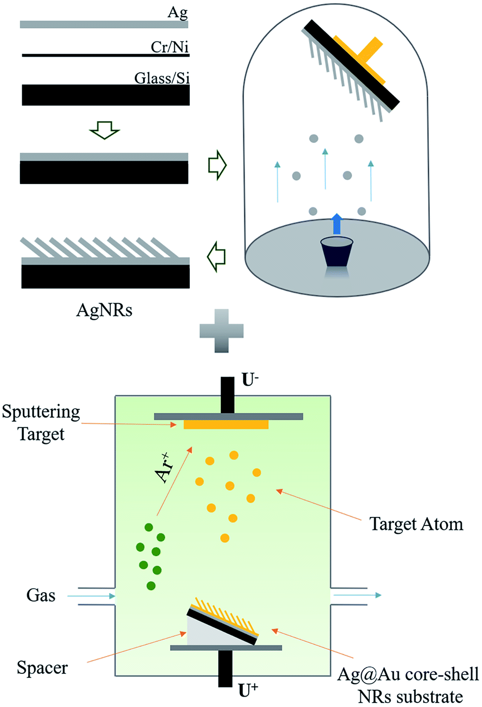
Herein, the AgNR substrate was prepared using the OAD process which has been reported in our previous work,35 this process is depicted in Fig. 1. First, the Si wafer was cleaned to facilitate the preparation of the AgNR structure. The structure was fabricated in three steps. A 20 nm-thick Ti layer was first plated on the Si wafer to increase the adhesion of the Ag film to the substrate. Then, a 200 nm-thick Ag layer was deposited on the Ti layer to enhance the adsorption of the columnar structure on the surface. Subsequently, the AgNR array was prepared at a tilting deposition angle of 86°. The tilting angle refers to the angle between the normal direction of the wafer and the direction of the evaporation source. The Au shell in the core–shell structure was realised using sputtering technology. In the sputtering process, Au atoms separated from the target under the bombardment of argon ions that will fill the whole vacuum chamber and move randomly. The random collision between Au atoms and Ag nanorods makes it possible to form an Au shell outside the Ag nanorods. During processing, the prepared AgNR substrate was attached to the sputtering stage using a high-temperature adhesive tape. And, the AgNR substrate was kept at a sputtering deposition angle of 10° by adding spacers, so that the nanorods were kept facing the sputtering target vertically. Thus, the chance of contacting Au atoms in any part of the whole nanorod is the same, even the back side of the Ag nanorod pointing away from the Au target can get an effective Au coating. This process ensures the formation of Au shells on AgNRs. Then, Au shells with different thicknesses were coated on AgNRs by controlling the sputtering parameters. In the experiments, three coating thickness of the Au shell, i.e., δ = 10 nm, 20 nm and 30 nm were adopted.
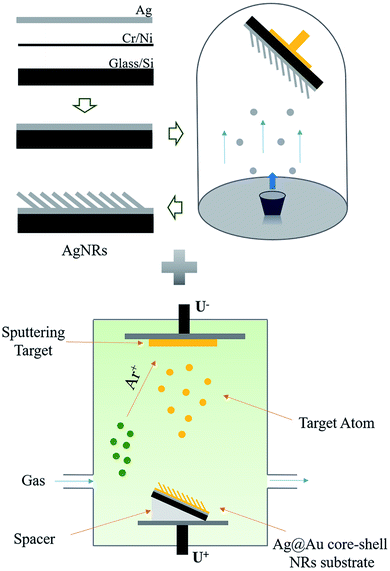 |
| | Fig. 1 Schematic of the fabrication process of the Ag@Au core–shell NR array substrate. | |
2.4. FDTD modelling
To simulate the Ag@Au core–shell NR array, the FDTD method was used (Fig. 2). A Cartesian coordinate system was established. The Z axis was the direction normal to the substrate, the Y axis was the growth direction along the Ag@Au core–shell NRs and the axis perpendicular to the Z and X axes. To simplify the model and reduce the calculation time, only three rows and columns of the Ag@Au NR array were used. The simulation area surrounded the entire model. The size of the Si wafer in the model was 1500 × 2400 nm2. According to the actual experimental parameters, Ti (20 nm) and Ag layers were fabricated on the Si wafer surface. In the Ag@Au NR array structure, the diameter, length and tilt angle of AgNRs were set to 120 nm, 800 nm and 73°, respectively. The distances between two NRs along the X and Y axes were 200 nm and 600 nm, respectively. The parameters of AgNRs set in the FDTD simulation analysis were obtained based on real experimental results. The simulation model of the Ag@Au NR array structure was obtained by changing the thickness parameters of the Au shell coated on the AgNR surface. The Au film thickness was set as 10, 20 and 30 nm. To comply with the actual situation, a Au layer of corresponding thickness was simultaneously added on the substrate surface. The grid division accuracy was 2 × 2 × 2 nm3. The absorbing boundary conditions of the perfectly matched layer were used in the X, Y and Z axes. The plane wave with a wavelength of 785 nm was used as the laser source, which was perpendicular to the substrate. Furthermore, the polarisation direction was parallel to the X axis.
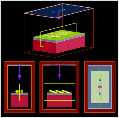 |
| | Fig. 2 Models of the Ag@Au core–shell NR array substrate. | |
2.5. Raman measurements
Raman spectra were obtained using the Raman microscope. A 785 nm semiconductor laser was used as the excitation source. The integration time of each SERS detection was 10 s and the laser power was approximately 60 mW. All the SERS spectra used to depict the curve were background-subtracted. Three spots were randomly selected from the substrate, and the average value was considered as the final data value. BPE was used as the probe to characterise the properties of the Ag@Au core–shell NR array substrate. The spectra were obtained using the Raman microscope after the sample solution was dried in air.
3. Results and discussion
3.1. FDTD theoretical simulation
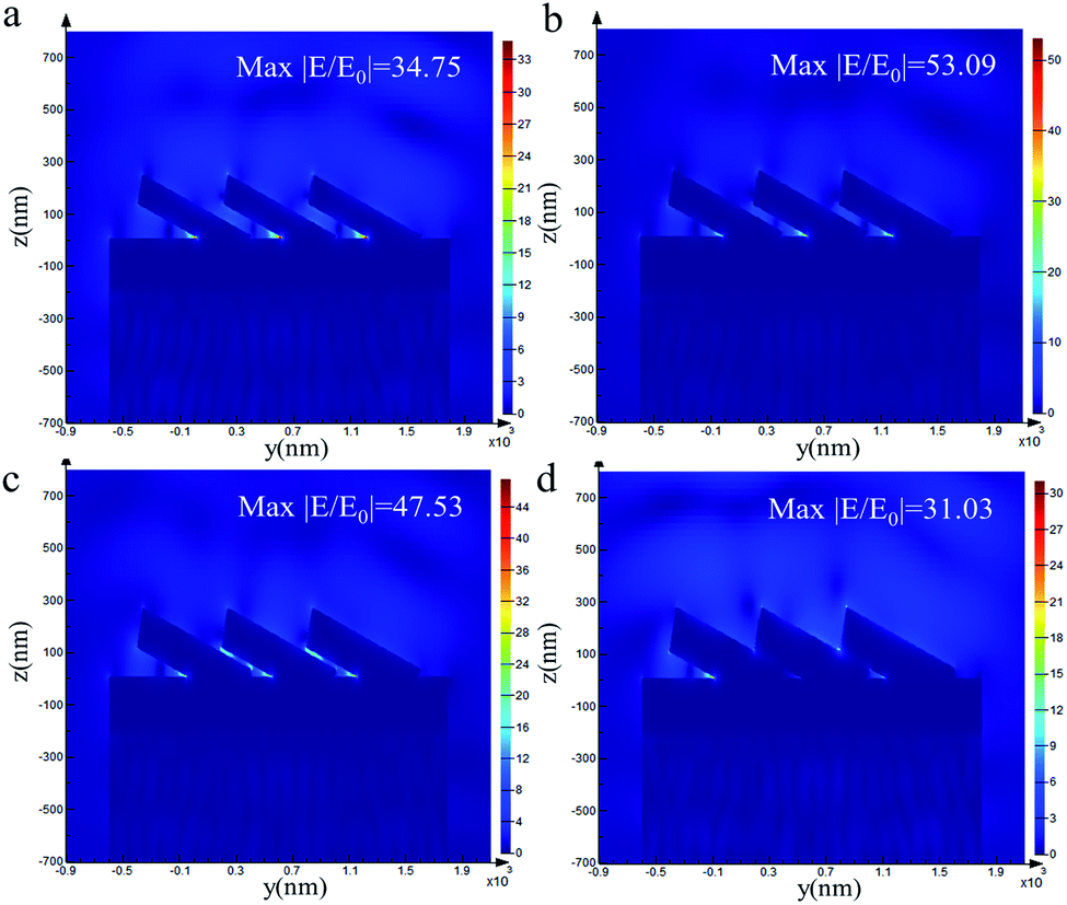
To verify the influence of the thickness of the Au film on Ag@Au NRs core–shell array substrate, the electromagnetic (EM) field distribution was visualised using FDTD calculations. The model and simulation parameters have been introduced in the previous section. Fig. 3 shows the EM field distribution of the AgNR substrate and Ag@Au NR array substrate with different thicknesses Au shells. The EM field distribution was similar for the Au shells with different thicknesses. The ‘hot spots’ were mainly concentrated in the gaps between adjacent NRs, the connections between the NRs and the underlying Au film and the tips of the NRs.
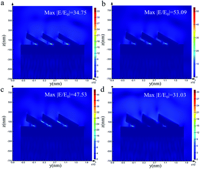 |
| | Fig. 3 Calculation results of NR array substrate with different shell thicknesses using the FDTD method (a) AgNRs, (b) Ag@Au NRs, shell, 10 nm, (c) Ag@Au NRs, shell, 20 nm, (d) Ag@Au NRs, shell, 30 nm. | |
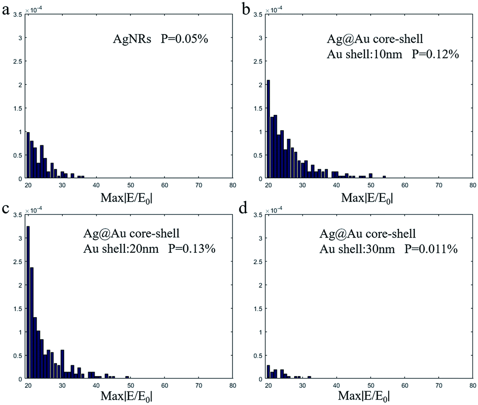
The maximum EM field intensity (max|E/E0|) values for Au shells with thicknesses of δ = 0, 10, 20 and 30 nm were 34.75, 53.09, 47.53 and 31.03, respectively. When the thickness of the Au shell was between 10 and 20 nm, the max|E/E0| value of the Ag@Au NR array substrate remained almost the same, which was in the range of 45–55. The FDTD calculation results proved that the max|E/E0| is increased to a certain extent when the Ag nanorods are coated with a reasonable thickness of the Au shell. And the results showed that the max|E/E0| value of the 10 nm-thick Au shell was the largest. Meanwhile, it is noticed that there is no significant difference in the max|E/E0| between the two cases of 10 and 20 nm Au shell. However, this may be the case when the intensity value of individual hot spots is large in the model calculation. In order to further study the influence of different Au shell thicknesses on the overall distribution of hot spots in substrate, the distribution of EM field intensity P within the range of 20–80 was statistically analyzed, as shown in Fig. 4. It is assumed that the total number of EM field intensity data points in the simulation area is N and the number of data points in the interval 20–80 is N1. The value of P (P = N/N1) represents the proportion of EM field intensity between the interval 20 and 80. The EM field density is greater when the P value is greater. For the film thickness of Au shell δ = 0, 10, 20 and 30 nm, the EM field density was 0.05%, 0.12%, 0.13% and 0.011%, respectively. With the increase of Au shell thickness, the EM field density first increases and then decreases. The EM field density is the highest when the Au shell thickness is 20 nm. This means that the substrate could provide more hot spots. Overall, the simulation results show that the SERS effect of the AgNR substrate may be improved by changing the spacing between the nanorods through coating Au shell. Meanwhile, from the process preparation perspective, the 10 nm-thick Au shell may not be completely coated. Additionally, the distance between the NRs was considerably reduced when the Au shell thickness reached 30 nm. This may cause the NRs to stick together, thereby reducing the EM field strength. Based on the simulation results and actual process conditions, 20 nm was finally selected as the Au shell thickness.
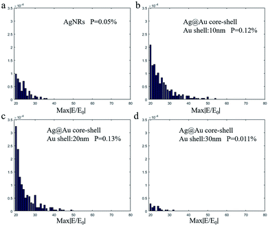 |
| | Fig. 4 Electromagnetic field density of the NR array substrate. | |
3.2 . Morphologies of the Ag@Au NR array structure
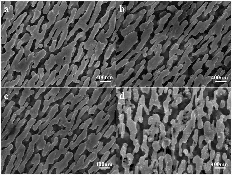
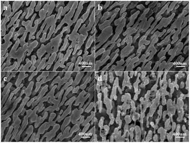
The morphology and elemental analysis were studied using SEM and TEM. Fig. 5a is the SEM image of the AgNR substrate. Fig. 5b–d present the SEM images of Ag@Au NR array structures with Au shells with different thicknesses. The SEM magnification of all structures is 20![[thin space (1/6-em)]](https://www.rsc.org/images/entities/char_2009.gif) 000×. The prepared substrate exhibits a periodic NR array structure. The spacing between the NRs gradually decreased as the thickness of the Au film increased, and the diameter of the NRs changed considerably. Fig. 5e presents the cross-sectional view of the Ag@Au NR array structure with a 20 nm-thick Au shell. The periodic and normal distributions the Ag@Au NR array structure were also observed. The NR length was approximately 850 ± 50 nm, and the tilt angle was 73° ± 2°. The sputtering scheme of the 20 nm-thick Au shell was selected based on simulation results and processing technology. The morphology of the AgNRs covered with Au shell was further studied using TEM.
000×. The prepared substrate exhibits a periodic NR array structure. The spacing between the NRs gradually decreased as the thickness of the Au film increased, and the diameter of the NRs changed considerably. Fig. 5e presents the cross-sectional view of the Ag@Au NR array structure with a 20 nm-thick Au shell. The periodic and normal distributions the Ag@Au NR array structure were also observed. The NR length was approximately 850 ± 50 nm, and the tilt angle was 73° ± 2°. The sputtering scheme of the 20 nm-thick Au shell was selected based on simulation results and processing technology. The morphology of the AgNRs covered with Au shell was further studied using TEM.
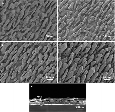 |
| | Fig. 5 Morphology of the NR array substrate (a) AgNRs, (b) Ag@Au core–shell, shell-10 nm, (c) Ag@Au core–shell, shell-20 nm, (d) Ag@Au core–shell, shell-30 nm, (e) Ag@Au core–shell, shell-20 nm, cross-sectional view. | |
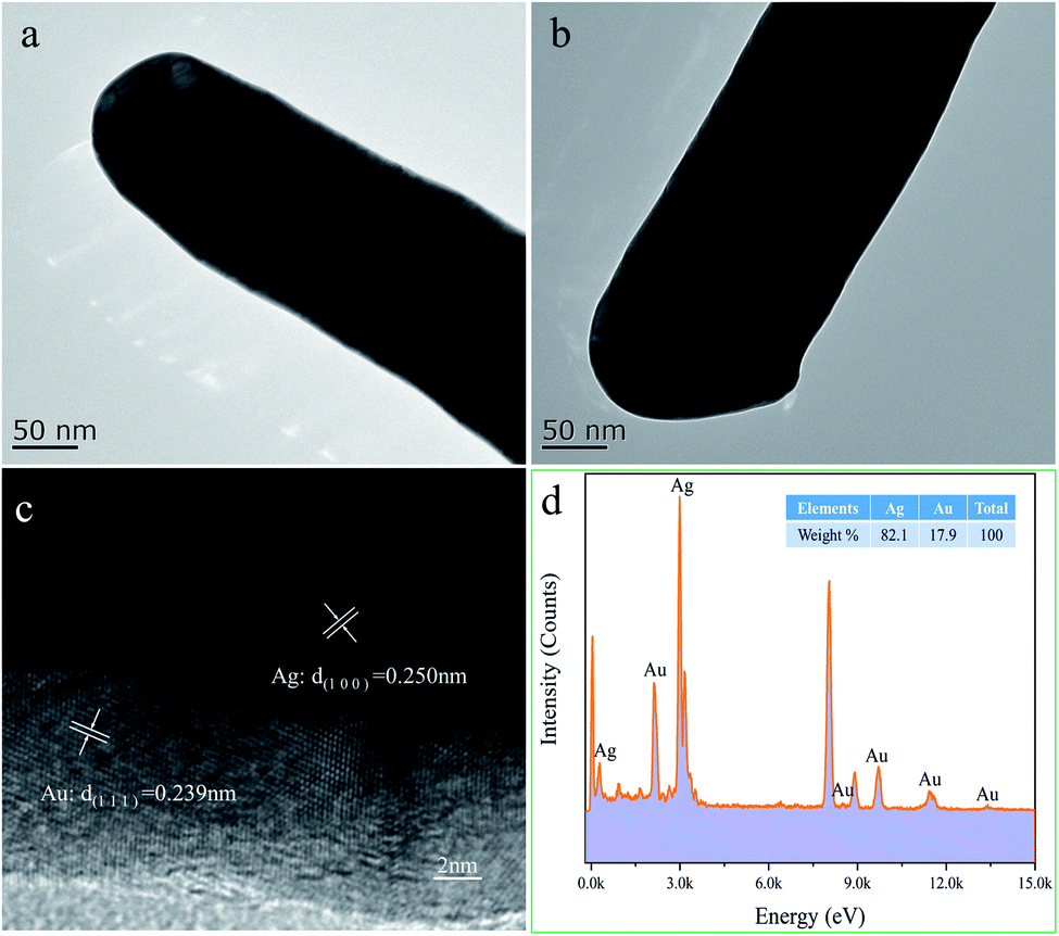
Fig. 6a and b demonstrate the TEM images of Ag@Au NR array substrate coated with 10 nm-thick and 20 nm-thick Au shells, respectively. The surface of the substrate after sputtering is smooth and continuous. Furthermore, to investigate the distribution of Au in the shell, high resolution transmission electron microscope (HRTEM) characterization was carried out. Therefore, the Ag@Au NR array substrate with 10 nm-thick Au shell were characterized to prove the existence of the Au shell. Fig. 6c reveals the (100) lattice planes of Ag and (111) lattice planes of Au. The HRTEM image confirms that Au shell is homogeneously distributed in the Ag nanorods. With the increase of the thickness of the sputtered Au, the formation of the Au shell outside the Ag nanorods is ensured.
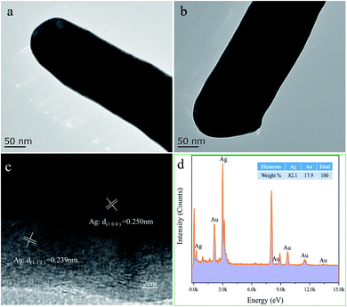 |
| | Fig. 6 TEM images of Ag@Au core–shell NR structure, (a) TEM image of 10 nm-thick Au shell substrate, (b) TEM image of 20 nm-thick Au shell substrate, (c) HRTEM image of 10 nm-thick Au shell substrate, (d) X-ray energy-dispersive spectroscopy (EDS) of 20 nm-thick Au shell substrate. | |
Furthermore, the distribution of each element in the Ag@Au NR array substrate can be determined by field-emission TEM characterization. Fig. 6d shows the X-ray energy-dispersive spectroscopy (EDS) of Ag@Au NR array substrate with 20 nm-thick Au shell, which illustrates the composition of the Ag@Au NR array substrate. Moreover, to further document the presence of Ag and Au in Ag@Au NR array substrate, the corresponding elemental mappings were performed. Fig. 7a exhibits a typical scanning TEM characterization mapping of the Ag@Au NR array substrate. Fig. 7b shows that Au and Ag are evenly distributed on the Ag@Au NR array substrate. As can be seen, the Au shell layer was evenly coated on the AgNRs with a thickness of 20 ± 3 nm. Fig. 7c and d display the elemental mapping of Ag and Au, respectively. Based on the above experimental findings, the Ag@Au NR array substrate with a uniform coating Au was successfully prepared using the sputtering technology.
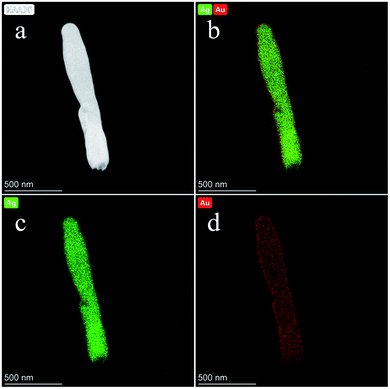 |
| | Fig. 7 Characterization of the Ag@Au core–shell NR structure with 20 nm-thick Au shell. (a) STEM image of substrate. (b) Elemental mapping image of substrate. (c) Elemental mapping image of Ag. (d) Elemental mapping image of Au. | |
3.3. Performance analysis
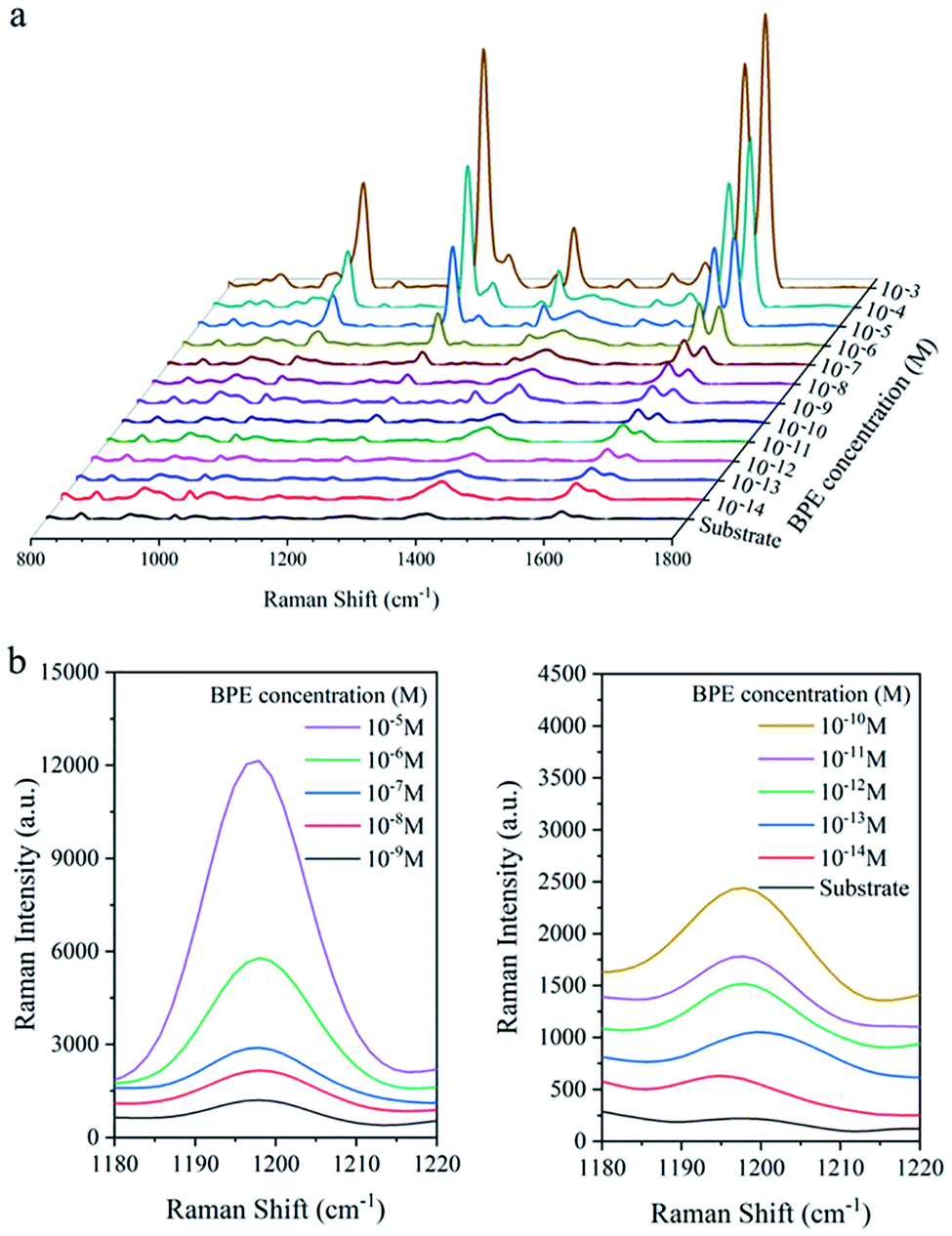
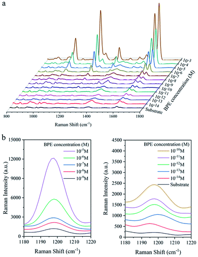
To characterise the SERS performance of Ag@Au NR array substrate, a series of BPE ethanol solutions with concentrations of 10−13 M to 10−3 M was detected using Ag@Au NR array substrate with a 20 nm-thick Au shell. As shown in Fig. 8a, the characteristic peaks of BPE appeared at 1198, 1604 and 1637 cm−1 in the SERS spectra, which were consistent with the literature.36 And, the Raman intensity of the characteristic peaks gradually decreased with a decrease in the BPE concentration. The characteristic peak at 1198 cm−1 was selected. The detailed changes in the BPE spectra from 1180 to 1220 cm−1 were studied (Fig. 8b). When the concentration of BPE was 10−13 M, the characteristic intensity of BPE at 1198 cm−1 was not obvious. Because the spectral signal-to-noise ratio was >3, our experimental results are convincing and the LOD of the Ag@Au NR array substrate for BPE was 10−12 M.
 |
| | Fig. 8 SERS performance analysis of the Ag@Au NR array substrate. (a) SERS spectra of different concentrations of BPE. (b) Details of BPE spectra in the range of 1180–1220 cm−1. | |
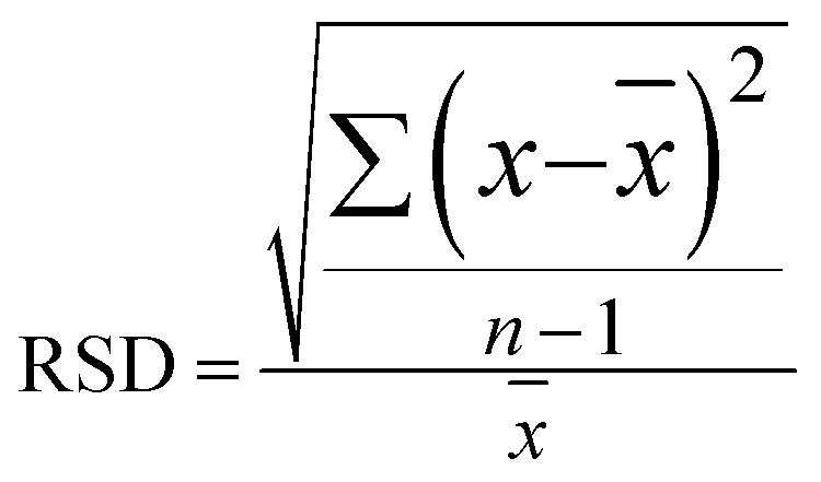
Furthermore, using BPE ethanol solutions with a concentration of 10−5 M, the uniformity of the SERS signal for the Ag@Au NR array substrate was analysed. For testing, 20 points were randomly selected on the surface of the core–shell structure. As shown in Fig. 9a, the characteristic peaks of BPE appeared at 1198, 1604 and 1637 cm−1 in the SERS spectra as the reference. Moreover, the obtained spectra showed good uniformity for the as-prepared substrate. Then, using the characteristic peak of the BPE molecule at 1198 cm−1 as a reference, a histogram of the Raman intensity was depicted in Fig. 9b. After statistical analysis, the relative intensity of the Raman spectra was found to be concentrated between 4700 and 5400. Further, the relative standard deviation (RSD) was used to measure the dispersion of the SERS spectral intensity. The RSD is calculated using the following formula:
| |
 | (1) |
where
![[x with combining macron]](https://www.rsc.org/images/entities/i_char_0078_0304.gif)
and
n are the average value and the number of samples, respectively. The calculation results showed that the RSD of the substrate at 1198 cm
−1 was ∼7.51%. The degree of dispersion conformed to the SERS detection requirements, further proving that the Ag@Au NR array substrate has good uniform performance.
 |
| | Fig. 9 Uniformity of the Ag@Au NR array substrate. (a) SERS spectra of BPE sampled at 20 random points. (b) Raman intensity distribution at the Raman shift of 1198 cm−1. | |
To simulate and verify the oxidation resistance of the Ag@Au NR array substrate, the Ag@Au NR array substrate and the AgNR SERS substrate were immersed in a 2% H2O2 solution for 1 h, respectively. The morphology of the Ag@Au NR array NR substrate and AgNRs was observed before and after treatment (Fig. 10). The morphology of the core–shell NR substrate showed no obvious change; however, the AgNRs were corroded by H2O2 and defects appeared on them. The experimental results also indirectly indicate the integrity of the coated Au shell. The structural integrity of AgNRs can be effectively protected in harsh environments by coating AgNRs with an Au shell.
 |
| | Fig. 10 SEM images of NR substrate. (a) Ag@Au NR array substrate before H2O2 treatment. (b) Ag@Au NR array substrate after H2O2 treatment. (c) AgNR substrate before H2O2 treatment. (d) AgNR substrate after H2O2 treatment. | |
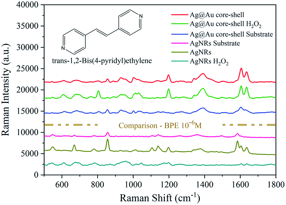
Then, a 10−6 M BPE solution was used to evaluate the SERS performance of the two types of substrates before and after H2O2 treatment. Fig. 11 shows the comparison of the intensity of two sets of SERS spectra. After H2O2 treatment, the SERS signal corresponding to the Ag@Au NR array substrate decreased slightly, whereas that of the AgNR substrate decreased considerably. Based on the above experimental findings, the complete coating of the Au film on AgNRs not only maintains the good SERS performance of the AgNR structure but also improves the stability of the NR substrate. This could realise the improved long-term preservation and use of SERS substrate.
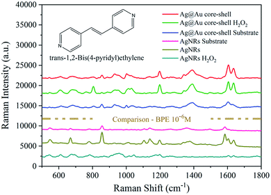 |
| | Fig. 11 Comparison of the performance of the Ag@Au NR array substrate and AgNR substrate before and after H2O2 treatment. (Inset) The molecular structure of BPE. | |
Furthermore, the SERS performance of the AgNR substrate and the Ag@Au NR array substrate coated with a 20 nm-thick Au shell was compared. It can be seen from Fig. 12 that the SERS effect of the Ag@Au NR array substrate is stronger than that of the pure AgNR substrate. This is also consistent with the FDTD calculation results. The results show that although Au has lower SERS activity than Ag, the SERS effect of the AgNR substrate may be improved by changing the spacing between the nanorods through coating Au shell. Then, the SERS performance comparison between the newly prepared Ag@Au NR array substrate and AgNR substrate and the old Ag@Au NR array substrate and AgNR substrate stored for 8 months in a vacuum package is also present in Fig. 12. As can be observed, the SERS signal of the AgNR substrate has been significantly reduced after 8 months. But SERS activity, when compared to that of the fresh and 8 months-old Ag@Au NR array substrate, is maintained well with aging. Comparing to AgNRs, the aged Ag@Au NR array substrate improved the stability of the substrate which had better performance for long life-times due to the presence of Au. It is demonstrated to be stable for SERS analysis.
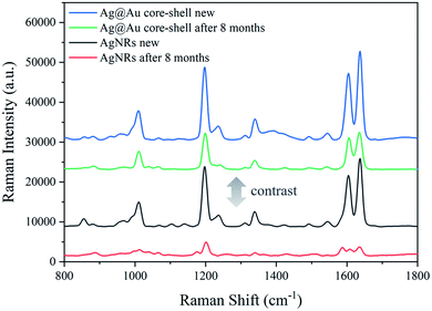 |
| | Fig. 12 Raman spectra of 10−3 M BPE: Ag@Au NR array substrate and AgNR substrate freshly prepared and 8 months old. | |
4. Conclusion
In this work, we combined the advantages of the AgNR structure (such as a simple preparation process and good repeatability) and the good chemical stability of Au materials to prepare an SERS substrate with good SERS performance and chemical stability. Using the OAD process and sputtering technology, we fabricated the Ag@Au core–shell NR array substrate. The SERS performance of the synthesised substrate could be improved by adjusting the thickness of the Au shell. According to the results of FDTD simulation analysis and the process compatibility, the 20 nm-thick Au shell was selected to cover the AgNRs. Furthermore, using BPE as the probe molecule to characterise the performance of the core–shell substrate, the LOD could reach 10−12 M. The RSD of the spectrum obtained for the substrate at the same concentration was 7.51%, showing good uniformity. And, stability of the Ag@Au NR array substrate was improved. Even under the strong oxidation of H2O2, the as-prepared Ag@Au NR array substrate could maintain better structural stability and SERS performance than the bare AgNRs. Moreover, the Ag@Au NR array substrate still has good SERS activity even after 8 months stored in a vacuum package. The method used herein maintains the structure of the AgNR substrate as well as the stability of Au. The Ag@Au core–shell NR array substrate has considerable potential in realising a simple, stable and repeatable preparation of the SERS substrate.
Author contributions
Pengxing Sha: conceptualization, investigation, software, writing-original draft. Qingqing Su: methodology, investigation, software. Peitao Dong: conceptualization, writing – review & editing, supervision, project administration, funding acquisition. Tianran Wang: visualization, investigation, formal analysis. Chushu Zhu: visualization, formal analysis. Weiye Gao: visualization, formal analysis. Xuezhong Wu: resources, writing – reviewing and editing, funding acquisition.
Conflicts of interest
The authors declare that they have no known competing financial interests or personal relationships that could have appeared to influence the work reported in this paper.
Acknowledgements
This research was funded by the National Natural Science Foundation of China (No. 51475468 and 51605486).
References
- G. Duncan and G. Royston, Chem. Soc. Rev., 2008, 37, 883–884 RSC.
- J. H. Granger, N. E. Schlotter, A. C. Crawford and M. D. Porter, Chem. Soc. Rev., 2016, 45, 3865–3882 RSC.
- M. Su, Q. Jiang, J. Guo, Y. Zhu, S. Cheng, T. Yu, S. Du, Y. Jiang and H. Liu, LWT, 2021, 143, 111143 CrossRef CAS.
- W. Fang, B. Zhang, F.-Y. Han, Z.-N. Qin, Y.-Q. Feng, J.-M. Hu and A.-G. Shen, Anal. Chem., 2020, 92, 13539–13549 CrossRef CAS PubMed.
- Y. Ma, H. Liu, M. Mao, J. Meng, L. Yang and J. Liu, Anal. Chem., 2016, 88, 8145–8151 CrossRef CAS.
- V. Marlitt, R. S. T, S. Kuldeep, S. M. S, A. T. S, R. Tomas, Z. Kinga and B. Anja, Anal. Chem., 2020, 92, 4317–4325 CrossRef PubMed.
- N. Hussain, H. Pu, A. Hussain and D.-W. Sun, Spectrochim. Acta, Part A, 2020, 236, 118357 CrossRef CAS.
- L.-B. Zhong, Q. Liu, P. Wu, Q.-F. Niu, H. Zhang and Y.-M. Zheng, Environ. Sci. Technol., 2018, 52, 5812–5820 CrossRef CAS PubMed.
- G. Xu, H. Cheng, R. Jones, Y. Feng, K. Gong, K. Li, X. Fang, M. A. Tahir, V. K. Valev and L. Zhang, Environ. Sci. Technol., 2020, 54, 15594–15603 CrossRef CAS.
- S. Nie and S. R. Emory, Science, 1997, 275, 1102 CrossRef CAS PubMed.
- M. J. Banholzer, J. E. Millstone, L. Qin and C. A. Mirkin, Chem. Soc. Rev., 2008, 37, 885–897 RSC.
- P. Rajapandiyan, L. Guo-Kun, W. Yao-Hui, L. Jun-Yang, D. Song-Yuan, L. Jian-Feng, W. De-Yin and T. Zhong-Qun, Chem. Commun., 2017, 54, 10–25 Search PubMed.
- S. Jradi, L. Zaarour, Z. Chehadi, S. Akil and J. Plain, Langmuir, 2018, 34, 15763–15772 CrossRef CAS.
- Z. Li, Z. Du, K. Sun, X. He and B. Chen, RSC Adv., 2017, 7, 53157–53163 RSC.
- B. Song, Z. Jiang, Z. Liu, Y. Wang, F. Liu, S. B. Cronin, H. Yang, D. Meng, B. Chen, P. Hu, A. M. Schwartzberg, S. Cabrini, S. Haas and W. Wu, ACS Nano, 2020, 14, 14769–14778 CrossRef.
- L. F. Tadesse, C. S. Ho, D. H. Chen, H. Arami, N. Banaei, S. S. Gambhir, S. S. Jeffrey, A. A. E. Saleh and J. Dionne, Nano Lett., 2020, 20, 7655–7661 CrossRef CAS.
- S. Lohumi, H. Lee, M. S. Kim, J. Qin and B. K. Cho, Anal. Bioanal. Chem., 2018, 410, 5663–5673 CrossRef CAS.
- T. Qiu, W. Zhang and P. K. Chu, Phys. B, 2009, 404, 1523–1526 CrossRef CAS.
- Z.-Q. Tian, B. Ren and D.-Y. Wu, J. Phys. Chem. B, 2002, 106, 9463–9483 CrossRef CAS.
- J. D. Driskell, S. Shanmukh, Y. Liu, S. B. Chaney, X. J. Tang, Y. P. Zhao and R. A. Dluhy, J. Phys. Chem. C, 2008, 112, 895–901 CrossRef CAS.
- Y. P. Zhao, S. B. Chaney, S. Shanmukh and R. A. Dluhy, J. Phys. Chem. B, 2006, 110, 3153–3157 CrossRef CAS PubMed.
- M. Subr, M. Petr, V. Peksa, O. Kylian, J. Hanus and M. Prochazka, J. Nanomater., 2015, 2015, 729231 Search PubMed.
- A. Rajput, S. Kumar and J. P. Singh, Analyst, 2017, 142, 3959–3966 RSC.
- M.-K. Oh, Y.-S. Shin, C.-L. Lee, R. De, H. Kang, N. E. Yu, B. H. Kim, J. H. Kim and J.-K. Yang, Nanoscale Res. Lett., 2015, 10, 259 CrossRef PubMed.
- D. Cai, Y. Mo, X. Feng, Y. He and S. Jiang, Appl. Surf. Sci., 2017, 406, 277–284 CrossRef CAS.
- N. H. Kim, S. J. Lee and K. Kim, Chem. Commun., 2003, 724–725 RSC.
- M. Suzuki, K. Nakajima, K. Kimura, T. Fukuoka and Y. Mori, Anal. Sci., 2007, 23, 829–833 CrossRef CAS.
- B. Li, T. Wang, Q. Su, X. Wu and P. Dong, Sensors, 2019, 19, 3742 CrossRef CAS.
- L. Ma, Y. Huang, M. Hou, Z. Xie and Z. Zhang, Sci. Rep., 2015, 5, 15442 CrossRef CAS.
- L. Ma, Y. Huang, M. Hou, J. Li, Z. Xie and Z. Zhang, J. Phys. Chem. C, 2016, 120, 606–615 CrossRef CAS.
- E. C. Cho, P. Camargo and Y. Xia, Adv. Mater., 2010, 22, 744–748 CrossRef CAS PubMed.
- C. Song, J. L. Abell, Y. He, S. Hunyadi Murph, Y. Cui and Y. Zhao, J. Mater. Chem., 2012, 22, 1150–1159 RSC.
- A. Gutés, R. Maboudian and C. Carraro, Langmuir, 2012, 28, 17846–17850 CrossRef.
- U. Waiwijit, C. Chananonnawathorn, P. Eimchai, T. Bora, G. L. Hornyak and N. Nuntawong, Appl. Surf. Sci., 2020, 530, 147171 CrossRef CAS.
- J. Chen, P. Dong, C. Wang, C. Zhang, J. Wang and X. Wu, Nano, 2017, 12, 1750131 CrossRef CAS.
- L. Zhou, S. Poggesi, G. Casari Bariani, R. Mittapalli, P. M. Adam, M. Manzano and R. E. Ionescu, Biosensors, 2019, 9, 53 CrossRef CAS PubMed.
Footnote |
| † Both authors contributed equally to this work. |
|
| This journal is © The Royal Society of Chemistry 2021 |
Click here to see how this site uses Cookies. View our privacy policy here. 
 Open Access Article
 This Open Access Article is licensed under a Creative Commons Attribution-Non Commercial 3.0 Unported Licence
 *,
Tianran Wang,
Chushu Zhu,
Weiye Gao and
Xuezhong Wu
*,
Tianran Wang,
Chushu Zhu,
Weiye Gao and
Xuezhong Wu