
 Open Access Article
 This Open Access Article is licensed under a Creative Commons Attribution-Non Commercial 3.0 Unported Licence
Fabrication optimization and application of 3D hybrid SERS substrates†
Xiaoyuan Gengab,
Chen Wuab,
Siying Liuabd,
Yu Hanab,
Liang Song*abc and
Yun Zhang *abcd
*abcd
aCAS Key Laboratory of Design and Assembly of Functional Nanostructures, Fujian Provincial Key Laboratory of Nanomaterials, Fujian Institute of Research on the Structure of Matter, Chinese Academy of Sciences, Fuzhou 350002, P. R. China. E-mail: songliang@fjirsm.ac.cn; zhangy@fjirsm.ac.cn
bXiamen Institute of Rare Earth Materials, Haixi Institute, Chinese Academy of Sciences, Xiamen Key Laboratory of Rare Earth Photoelectric Functional Materials, Xiamen 361021, P. R. China
cGanjiang Innovation Academy, Chinese Academy of Sciences, Jiangxi 341000, P. R. China
dUniversity of Chinese Academy of Sciences, Beijing 100049, P. R. China
First published on 22nd September 2021
Abstract
Three-dimensional (3D) plasmonic nanostructures with nanoparticles that can be tuned have got a lot of attention in surface-enhanced Raman scattering (SERS) due to the unique 3D plasmonic coupling. Here, two nanoparticles, gold nanosphere (AuNS) and gold nanooctahedra (AuNO), were used to construct 3D hybrid SERS substrates to investigate the effect of nanoparticle spatial position on the SERS performance of the 3D nanostructure and to obtain 3D substrates with high SERS activity. And more hybrid combination possibilities were tested to explore the variation trend of hot spots generated when the nanoparticles were near. First, two-dimensional (2D) planar substrates were prepared using the air–liquid interface-assisted self-assembly method, to examine the effect of nanoparticle size on SERS performance. Then, 3D hybrid SERS substrates were further prepared layer by layer to discuss the effect of different combination methods within three layers on SERS performance. The optimized 3D hybrid substrate with the sandwich structure of AuNS/AuNO/AuNS performed the strongest SERS enhancement effect, whose intensity was 4.1 and 1.9 times that of AuNS/AuNS/AuNS and AuNO/AuNO/AuNO, respectively, and had good reproducibility (relative standard deviation (RSD) of 1.08%). Furthermore, the thiram molecular result showed that the prepared AuNS/AuNO/AuNS had good linear relationship (R2 of 0.991) and good molecule detection sensitivity (the minimum detection volume of thiram is 100 ppb), which demonstrated the great potential of the 3D hybrid SERS substrates in practical analysis.
1. Introduction
Surface-enhanced Raman scattering (SERS) is a phenomenon in which the vibration spectrum of molecules adsorbed on a specific surface is greatly amplified. The amplification of the local electromagnetic field, particularly the hot spots formed from the near-field coupling effect between nanoparticles caused by the excitation of surface metal molecules which originates from the localized surface plasmon resonance (LSPR), results in such high enhancement effect.1–4 It has been proved that a small number of probe molecules falling on the hot spot region of the substrate provide a considerable portion of the SERS signal, showing that hot spots play a dominant role in SERS.5 Previous work on SERS has been mostly focused on investigating hot spots and fabricating structures with high enhancement effects, such as zero-dimensional (0D), one-dimensional (1D), two-dimensional (2D), and three-dimensional (3D) structures.6–8 However, high enhancement structures and enrichment of molecules under detection have many challenges.9–11 Meanwhile, the 3D structures have got a lot of attention as a novel type of SERS substrates. By increasing plasmonic coupling in the vertical direction (z-axis) based on a 2D plane, the distribution of hot spots expands from 2D plane to 3D volume, and the 3D plasmonic coupling, which becomes a unique feature of 3D structures contributes to multi-density hot spots and plays a key role in the SERS enhancement effect and high sensitivity of a 3D SERS substrate.12–16The effect of 3D plasmonic coupling includes in-plane and out-of-plane, which have been studied before. For example, Ünal et al. compared the 3D structure to its 2D counterpart structure, they found that the maximum surface-normal (out-of-plane) field enhancement greatly increased.17 Gong et al. confirmed that the hot spots existing in the whole depth (in-plane) positively affected SERS enhancement of the 3D SERS substrate.18 Our group has previously prepared several SERS substrates with different uniform nanoparticles, and the results show that the 3D substrates have better SERS enhancement performance than the 2D substrates of the same material.19,20 These results have revealed that the SERS enhancement effect of the 3D structure was significantly improved compared to the 2D counterpart substrate. However, our work on 3D substrates has only focused on the 3D assembly of single-morphology nanoparticles such as gold nanooctahedra (AuNO) and silver nanorod (AgNR), which is insufficient to investigate the 3D plasmonic coupling or to prepare high-performance 3D substrates. In addition, more 3D structures as needed have been designed and studied using metals21 or metal oxides,22 and materials like 2D materials and polymers, such as GO,23 WS2,24 cellulose25 and fibre.26 Among them, 3D structures prepared with nanoparticles and 2D materials have unique advantages in providing uniform signals and long-term stability.27 The 2D materials, in particular, have a definite thickness that could form a precise gap between the plasmonic nanostructures. The high electric field enhancement in the sub-nanometers gap could effectively improve the SERS enhancement effect of the entire substrates.28 However, surface modification is typically used for 2D materials to improve SERS enhancement performance and reduce substrate background signal. Metal nanoparticles with different morphologies can be used to prepare a 3D hybrid substrate and similarly control interlayer spacing in 3D substrates due to the relatively mature synthesis process of metal nanoparticles. Metal nanoparticles with different morphologies have different optical properties and SERS activity. For example, the SERS performance of a 3D substrate composed of AuNO performs better than that made of gold nanosphere (AuNS), because AuNO has more tunable morphological parameters compared to AuNS, including multiple atomically flat surfaces, well-defined edges and corners which were the sources of most hot spots.29,30 Studies have also shown that for 3D substrates using gold nanoparticles of the same size but different shapes, the SERS characteristics are significantly different.31 This indicates that changes in metal nanoparticles as structural units would affect the SERS performance of a 3D structure, which provides a foundation for research on the influence of metal nanoparticles with different morphologies on 3D substrates.
Furthermore, a high-reproducibility SERS substrate must match a suitable preparation method. Techniques like top-down and bottom-up methods are used primarily for the preparation of 3D SERS substrates in the past. Nanoscale devices are designed through traditional microfabrication methods (such as photolithography32) in a top-down method resulting in 3D SERS substrates with height-adjustable shape, good reproducibility and uniformity.33 However, it is difficult to manufacture substrates with a gap of less than 10 nm. Another simple and effective method for preparing 3D SERS substrates is bottom-up assembly technology, such as self-assembly, electrochemical deposition, and electrostatic adsorption, which involves assembling different nanostructures units on different substrates with precious metal nanoparticle self-assembly to create various types of ordered nanostructure SERS substrates. Conveniently, the shape and size of the assembly unit can be well regulated at a low cost and a short preparation time.34–36 The single-layer nanoparticles could be carefully laid on the air–liquid interface using the self-assembly technique, making it feasible to prepare various types of ordered nanostructures SERS substrates with different shapes of nanoparticles.20,37,38 Moreover, the layer-by-layer stacking of monolayer nanoparticles made it possible to fabricate structures with exact layers and study the correlation between 3D plasmonic coupling and SERS properties of the 3D hierarchical SERS19 or detect small biological molecules.20
A novel 3D hybrid SERS substrate introducing two different nanoparticles (AuNO, AuNS) was designed in this work. AuNO has a significant SERS enhancement effect because of its tunable plasmonic. AuNS was uniformly arranged when self-assembled on a 2D array with a curved surface making it a good choice for preparing a 3D substrate. The air–liquid interface-assisted self-assembly method was used to prepare 2D substrates made of monolayer nanoparticles (Scheme 1). And 4-MBA was used to evaluate the SERS activity of 2D substrates, then the optimal size of AuNS (45 nm) was selected to be assembled in different combinations with AuNO (89 nm) within three layers. To quantitatively detect molecular, dense 3D hot spots produced by 3D plasmonic coupling were used to enhance SERS signal. The uniformity of the substrate was investigated through SERS mapping, and the combination method AuNS/AuNO/AuNS with the best enhancement effect was determined. Finally, the detection of thiram with the minimum detectable concentration of 100 ppb and the detection of Malachite Green (MG) with the minimum detectable concentration of 10 nM was used to confirm the availability of the AuNS/AuNO/AuNS. This study provided an easy way to design and prepare hybrid 3D SERS substrates as a highly sensitive analytical tool for molecular detection in biochemical and food fields.
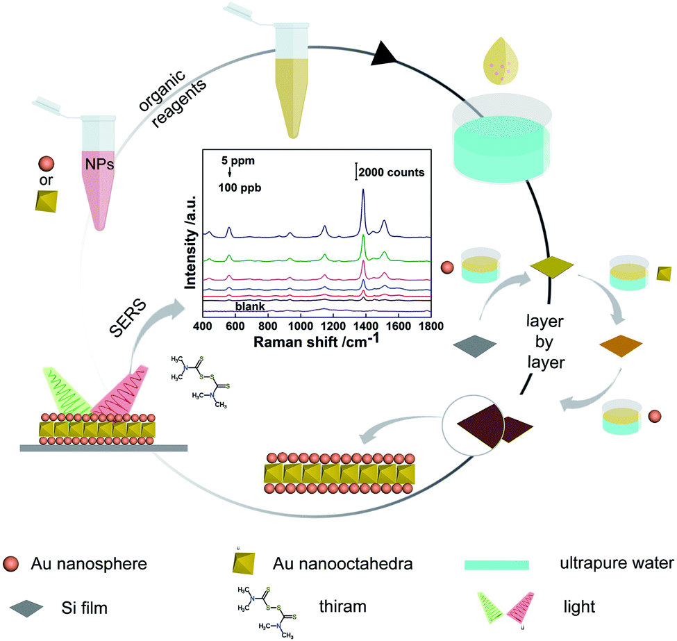 | ||
| Scheme 1 The schematic illustration of the process of a 3D hybrid SERS substrate for SERS analysis. | ||
2. Materials and methods
2.1 Materials
Hydrogen tetrachloroaurate trihydrate (HAuCl4·3H2O, 99%), sodium borohydride (NaBH4, 99%), poly(vinylpyrrolidone) (PVP, 55![[thin space (1/6-em)]](https://www.rsc.org/images/entities/char_2009.gif) 000), hexadecyl trimethyl ammonium bromide (CTAB, 99%), 4-mercaptobenzoic acid (4-MBA, 99%) and 3-butenoic acid (97%) were purchased from Sigma-Aldrich. Sodium oleate (NaOL, CP), hydrochloric acid (HCl, AR), silver nitrate (AgNO3, AR), and ascorbic acid (AA, 99.99%) were attained from Xilong Scientific Co., Ltd. All chemicals mentioned above were used without further purification. Milli-Q water (18.2 MΩ cm) was used throughout the study, and all glassware was cleaned with aqua regia and amounts of deionised water (DW) before use.
000), hexadecyl trimethyl ammonium bromide (CTAB, 99%), 4-mercaptobenzoic acid (4-MBA, 99%) and 3-butenoic acid (97%) were purchased from Sigma-Aldrich. Sodium oleate (NaOL, CP), hydrochloric acid (HCl, AR), silver nitrate (AgNO3, AR), and ascorbic acid (AA, 99.99%) were attained from Xilong Scientific Co., Ltd. All chemicals mentioned above were used without further purification. Milli-Q water (18.2 MΩ cm) was used throughout the study, and all glassware was cleaned with aqua regia and amounts of deionised water (DW) before use.
2.2 Methods
000 rpm for 40 min and washed with DW. The AuNS were dispersed into 1 mL DW. The larger diameter of AuNS was synthesised using small AuNS as seed, and the size of the AuNS was related to the volume of Au seeds added.2.3 Preparation of 3D hybrid substrates mediated by the air–liquid interface
1 mL AuNS (or AuNO) was mixed with 3 mL of 1% PVP ethanol solution. The mixture was sonicated for 3 h, washed with ethanol, and redispersed in 1 mL ethanol solution. Then 400 μL AuNS (or AuNO) ethanol solution was diluted with 400 μL dichloromethane, 400 μL cyclohexane, and 60 μL octane. The mixed solution was slowly dripped onto the surface of the water. The AuNS (or AuNO) monolayer was soon formed. After the solvent molecules had evaporated completely, a piece of silicon or glass was used to transfer the self-assembled monolayers and kept them dry in air at room temperature. After drying, another assembled monolayer was stacked continuously. Finally, 3D SERS substrates composed of AuNS and AuNO with different combination methods within three layers were obtained by repeating the process.2.4 Characterisation of the 2D and 3D substrates
The different sizes of AuNSs were characterised using transmission electron microscopy (TEM) (H-7650) and ultraviolet/visible/near-infrared (UV-vis-NIR) spectra (Agilent Cary 5000). SEM images of the substrates were acquired using a Hitachi S4800 microscope operated at 5 kV and an Apreo S LoVac microscope operated at 15 kV. The sizes of different nanoparticles were calculated by measuring more than 100 nanoparticles in TEM or SEM images using Image J software. The nanogap of near nanoparticles was calculated by measuring more than 100 spacing distances in SEM images using Image J software. The SERS activity of the 2D and 3D substrates was studied by an area SERS mapping (25 × 25 μm2 with 5 μm step) with 4-MBA as the probe. The 2D and 3D SERS substrates were soaked in 0.1 mM of 4-MBA ethanol solution for 2 h, then rinse with ethanol and dried at room temperature to remove any unbound molecules. Raman spectra were recorded on a LabRAM Aramis Raman microscope of Horiba JY. The 785 nm extinction line was focused on the substrate through a 10 × (NA = 0.25) objective. The Raman scattering light was collected using the same objective. The excitation wavelengths (633 nm, 785 nm) were focused on substrates with a power of 0.44 mW and 4.34 mW. The exposure time was 1 s for one mapping pixel.2.5 Quantitative SERS analysis of molecules
The optimized hybrid 3D SERS substrates AuNS/AuNO/AuNS (AuNS with a diameter of 45 nm and AuNO with a side length of 90 nm) were soaked in different concentrations of thiram and MG ethanol solution for 2 h. Specifically, thiram was detected at concentrations ranging from 100 ppb to 100 ppm, and MG from 10 nM to 10 μM. Then the substrates were washed with ethanol completely and dried at room temperature. To guarantee the accuracy and reliability of the detection, quantitative SERS analysis of thiram and MG was performed through the mapping area (25 × 25 μm2 with 5 μm step). All the Raman spectra were collected through a 10 × (NA = 0.25) objective, and the exposure time was 1 s. The excitation wavelength at the substrates was 633 nm laser with a power of 0.44 mW.3. Results and discussion
3.1 Synthesis and characterisation of AuNSs and AuNO
The synthesis of AuNSs with different diameters was based on the continuous growth method.40 By using small AuNS as seeds, a series of AuNSs with larger diameters were synthesised. The UV-vis-NIR spectra showed that the surface plasmon resonance (SPR) of the AuNSs was redshift from 520 nm to 532 nm as the diameter increased (Fig. 1A). The TEM images of the AuNSs are showed in Fig. 1B–F with corresponding diameters control 15.98 ± 0.64 nm, 29.82 ± 1.35 nm, 45.68 ± 1.99 nm, 54.67 ± 2.61 nm, 64.76 ± 2.46 nm, respectively. The synthesised AuNSs had good morphology and high dispersibility. However, when AuNS with a diameter over 64 nm was attempted to synthesise, the SPR of AuNS redshifted significantly (from 520 nm to 552 nm, Fig. S1A†), and the morphology of AuNS changed from nanosphere to nanopolyhedra (Fig. S1B†). It showed that after multiple growths, the morphology of nanoparticles would gradually change to more obvious polyhedrons and lose the morphology of the spheres. To minimise the influence of nanoparticle's morphology on the final result, these five AuNSs of different diameters with uniform size and good morphology were chosen for the subsequent study of the self-assembled 2D SERS substrates.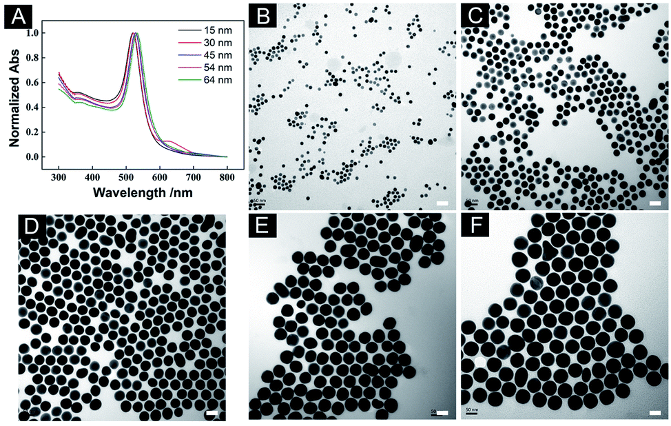 | ||
| Fig. 1 (A) The UV-vis-IR absorption spectra of AuNSs. (B–F) TEM images of the Au nanospheres with diameter control: (B) 15.98 ± 0.64 nm, (C) 29.82 ± 1.35 nm, (D) 45.68 ± 1.99 nm, (E) 54.67 ± 2.61 nm, (F) 64.76 ± 2.46 nm. The scale bars are 50 nm for all TEM images. | ||
The air–liquid interface-assisted self-assembly method was used to prepare the monolayer 2D substrates of AuNSs with different diameters. When the disposed solution was dropped on the water surface, the gold nanoparticles were closely packed and assembled to form a highly reflective monolayer film on the water surface, and then transferred to arbitrary substrates (Scheme 1). Five monolayer 2D SERS substrates self-assembled with five different diameters synthesised previously were prepared simultaneously to obtain the optimal diameters of AuNS, and the corresponding SEM images of the SERS substrate were shown in Fig. 2A–E. The AuNSs were dispersed on the substrates uniformly and tightly, without obvious cracking in a large area. The gap between two adjacent nanospheres was within a few nanometers, which was beneficial to the generation of hot spots (Table S1†). To compare the SERS performance of different substrates, 4-MBA was used as a probe molecule through a large area of SERS mapping at two wavelengths, and the comparison result was shown in Fig. 2F. As the diameter of the AuNSs increased, the corresponding SERS intensity showed a trend of first increasing and then decreasing, and the maximum intensity was achieved with the optimized diameter of 45.68 ± 1.99 nm. It was reported that in a series of AuNSs with diameters of less than 30 nm, the enhancement effect of single AuNS increased with the growth of the size.41 In this work, AuNS with a diameter of 45.68 ± 1.99 nm performed best in SERS enhancement, which might be the compromise size of AuNS in 2D plane was easy to obtain large SERS enhancement. Specifically, for the fixed laser irradiation area, it was impossible to contain more Au nanospheres of larger diameter, leading to fewer hot spots in the signal acquisition area. Furthermore, with diameters over 45.68 ± 1.99 nm, the AuNSs appeared to be more obvious growth of anisotropy, resulting in irregular spheres, which affected the arrangement in the 2D plane. In addition, the signal intensity excited by 785 nm was higher than that of 633 nm. In summary, the optimal size of AuNS (45.68 ± 1.99 nm) was used in the subsequent work.
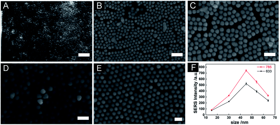 | ||
| Fig. 2 SEM images of AuNSs self-assembly with diameters of (A) 15.98 ± 0.64 nm, (B) 29.82 ± 1.35 nm, (C) 45.68 ± 1.99 nm, (D) 54.67 ± 2.61 nm, (E) 64.76 ± 2.46 nm. (F) SERS performance of monolayer AuNS substrates (A–E). The SERS intensity of 4-MBA at 1080 cm−1 was derived from the average value of the mapping areas (A–E). The scale bars are 100 nm for all SEM images. | ||
To realize the purpose of 3D hybrid SERS substrates, at least two kinds of nanoparticles were required. In our previous works, AuNO exhibited a large degree of regularity in the 2D monolayer assembly. There were also reports that the upward faces of AuNOs self-assembled on the 2D plane were almost uniform.19,42 Furthermore, AuNO had many clear edges and corners as tuning plasmonic material, which was critical for the formation of additional hot spots in the hybrid assembly structures and the SERS performance of substrates. Therefore, referring to the previous method, with the aid of gold nanorods (AuNRs) as seeds for secondary growth, AuNO was synthesised.19,39,43 As can be seen in the UV-vis-IR absorption spectra in Fig. 3A, the longitudinal dipolar plasmon resonance (LDPR) of AuNR (black) was measured at 929 nm. The absorption line reached the highest value at 600 nm (red) after being used for secondary growth to synthesise AuNO. Fig. 3B showed the TEM image of AuNRs with an average length of 89.10 ± 4.80 nm and an average diameter of 17.40 ± 1.70 nm (Fig. S2A and B†). The monolayer 2D substrate prepared by the air–liquid interface-assisted self-assembly method yields the SEM image of AuNO showed in Fig. 3C, with a TEM image in Fig. S2C† and a large area SEM image of the 2D substrate in Fig. S2D.† Typical self-assembled AuNO was on the substrate with one triangular plane facing up. Additionally, the overall 2D plane assembly of the AuNOs met the requirement for 3D hybrid assembly. The influence of AuNO side length on the corresponding SERS enhancement has been explored earlier by our group, and the superiority of AuNO with a side length of 90 nm in 3D SERS assembly has been determined.19 To this end, the AuNO with an average side length of 89.10 ± 4.80 nm was selected for the subsequent study of the 3D hybrid SERS performance.
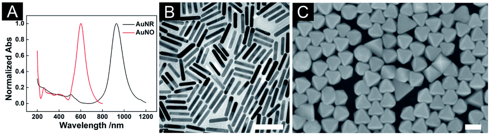 | ||
| Fig. 3 (A) The UV-vis-IR absorption spectra of AuNR (black) and AuNO (red). (B) TEM image of AuNR. (C) SEM image of AuNO self-assembly. The scale bars are 100 nm. | ||
3.2 Characterisation of AuNS and AuNO hybrid self-assembly substrates and 3D SERS performance
The optimized AuNS (45.68 ± 1.99 nm) and AuNO (89.10 ± 4.80 nm) were selected to prepare the 3D hybrid substrates to investigate their performance. As shown in Scheme 1, eight 3D substrates in various combinations were prepared at the same time through the layer-by-layer accumulation of monolayer 2D planes. Fig. 4A–H showed cross-sectional SEM images of all types of assembled 3D structures, and it was easy to find the successful three-layer structures, which indicated such an assembly method was feasible to prepare 3D hybrid substrates. The extinction spectra of 3D substrates with different combinations were showed in Fig. S3.† The resonance wavelengths exhibited in the extinction spectra of 3D substrates were almost at the wavelength region between 633 nm to 785 nm (the red and green dashed line in Fig. S3†). It indicated neither 633 nm or 785 nm could match the resonance wavelength of the substrate well. As previously stated, most AuNOs were assembled on a substrate with triangular plane facing up, ensuring that the opposite triangular plane was in contact with the substrate surface, which was verified from Fig. 4C that the AuNOs assembled in the bottom layer of 3D structure with triangular surfaces facing down. However, when the substrate surface was full of AuNSs, AuNOs will contact the curve surface of AuNSs with one triangular plane. In this study, when comparing the size of nanooctahedra to that of nanosphere, it took almost two nanospheres to equal one nanooctahedra in size (Fig. 4H), which meant more hot spots generated in nanoparticle–nanoparticle junctions when AuNO and AuNS were close.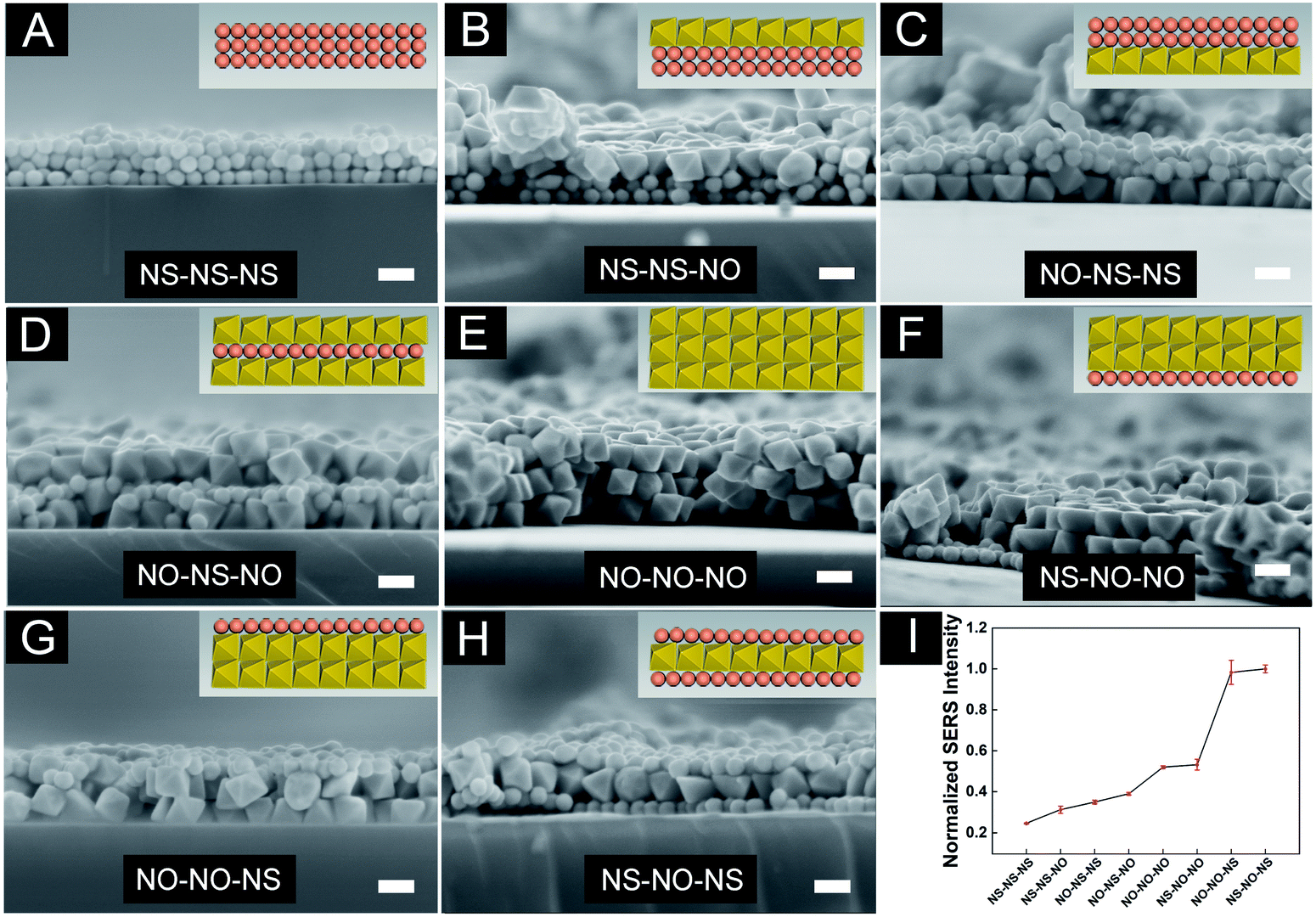 | ||
| Fig. 4 SEM images and SERS performance of the AuNS and AuNO 3D hybrid substrates. The cross-sectional view of the SEM images for the (A) AuNS/AuNS/AuNS, (B) AuNS/AuNS/AuNO, (C) AuNO/AuNS/AuNS, (D) AuNO/AuNS/AuNO, (E) AuNO/AuNO/AuNO, (F) AuNS/AuNO/AuNO, (G) AuNO/AuNO/AuNS, (H) AuNS/AuNO/AuNS. The insets are the 3D illustration. (I) Normalized SERS intensity for 3D hybrid substrates with different self-assembly combinations. The SERS intensity at 1080 cm−1 of 4-MBA were used for comparing the performance. The scale bars are 100 nm. | ||
Furthermore, the contact surfaces of the two AuNOs were triangular planes when two layers of AuNOs were assembled (Fig. 4G). When the three layers were all AuNOs (Fig. 4E), the arrangement of the AuNOs was more irregular, indicating more different forms of self-assembly, which were also consistent with earlier research that as the number of layers increases, the actual height of the 3D substrate was different from the total thickness of the monolayer in the ideal state, which indicated multiple orientations within one layer.19 In summary, the cross-sectional images verified the successful manufacturing of the 3D hybrid substrate. To further analyse the uniformity and reproducibility of 3D hybrid substrates, 4-MBA were used as Raman probe and the best-assembled nanostructure were determined from Fig. 4I, which showed normalised graph of SERS intensity of 4-MBA on eight substrates. The SERS intensity of 4-MBA at 1080 cm−1 detected in substrate AuNS/AuNO/AuNS was 4.1 times and 1.9 times of that in AuNS/AuNS/AuNS and AuNO/AuNO/AuNO, respectively. That showed the unique superiority of AuNS/AuNO/AuNS substrate.
It has been pointed out that the sphere diameter (or the curvature radius of the tip) should be tiny for a more confined region of the local electric field to achieve a strong local electric field.44 In other words, the sharper the tip, the easier it is to focus on the super-strong local electric field. When AuNO was assembled with AuNS in a 3D hybrid substrate, the triangular plane contacted the curved surface of the AuNS but contacted the triangular face of another AuNO when assembled with the same AuNO. Compared to the curved surface of AuNS, the triangular plane of the AuNO had a smaller radius of curvature. Therefore, it was easy to draw the inference that under the same conditions, the hot spot produced by the AuNO–AuNO junctions showed a weaker SERS intensity than that of the hot spot produced by the AuNO–AuNS junctions (only the hot spot at the particle contact site was compared here). Therefore, as shown in Fig. 4I, with the same three-layer nanostructure, AuNO/AuNO/AuNO exhibited the SERS enhancement effect far inferior to AuNS/AuNO/AuNS and AuNO/AuNO/AuNS. The SERS intensity of AuNS (45 nm) in this article under excitation of 785 nm was far inferior to that of AuNO (Fig. S4†), so the SERS performance of AuNO/AuNO/AuNO was stronger than that of AuNS/AuNS/AuNS (Fig. 4I). Additionally, Zhang et al. studied the exact location of hot spots in the 3D nanostructure, and they found that the precise location of the hot spot of the 3D substrate was related to the excitation laser. Specifically, under the excitation of 785 nm laser, the strongest signal was concentrated in the middle area of the 3D substrate.45 This meant that under the excitation of 785 nm laser, the hot spots generated by nanoparticles in the middle layer provide the dominant SERS enhancement effect. Among the different substrates assembled with AuNO and AuNS in this work, SERS enhancement of substrates with the middle layer of AuNO (Fig. 4E–H) was stronger than that of substrates with the middle layer of AuNS (Fig. 4A–D), which responded to the result that the SERS activity of AuNO under the laser of 785 nm was stronger than that of AuNS (Fig. S4†). Therefore, AuNS/AuNO/AuNS showed the best SERS enhancement effect. In addition, Fig. S5† showed that light transmittance of different 3D substrates was varied, which could be the size difference between AuNO and AuNS leading to the fine distinction of the thickness of substrates.
Another important feature of the 3D hybrid SERS substrates is good reproducibility. The reproducibility of the substrates of different combinations was evaluated by mapping the SERS intensities over an area of 25 × 25 μm2 with a scanning step of 5 μm at excitation wavelengths of 785 nm and an integration time of 1 s. Fig. 5A–H showed the SERS mapping of 4-MBA (10−4 mol L−1) with different substrates at the peak of 1080 cm−1. SERS spectra of 4-MBA detected by substrates with different combinations. The corresponding SERS spectra of 4-MBA detected by substrates with different combinations were shown in Fig. 5I. The SERS mapping images indicated a high uniformity of the 3D hybrid SERS structures, and the corresponding relative standard deviation (RSD) values were in the range of 1.08% to 5.00% across the mapping areas for excitation wavelengths of 785 nm, which were much smaller than those of the monolayer 2D SERS substrates and were up to an excellent standard (less than 10.00%) for requiring a commercial SERS substrate.46,47 From the results, we could conclude that the SERS substrates conducted with AuNO and AuNS exhibited excellent uniformity of the SERS signal over a large area, which benefited from the compact structure prepared by air–liquid interface-assisted self-assembly manner and the uniform size of AuNO and AuNS.
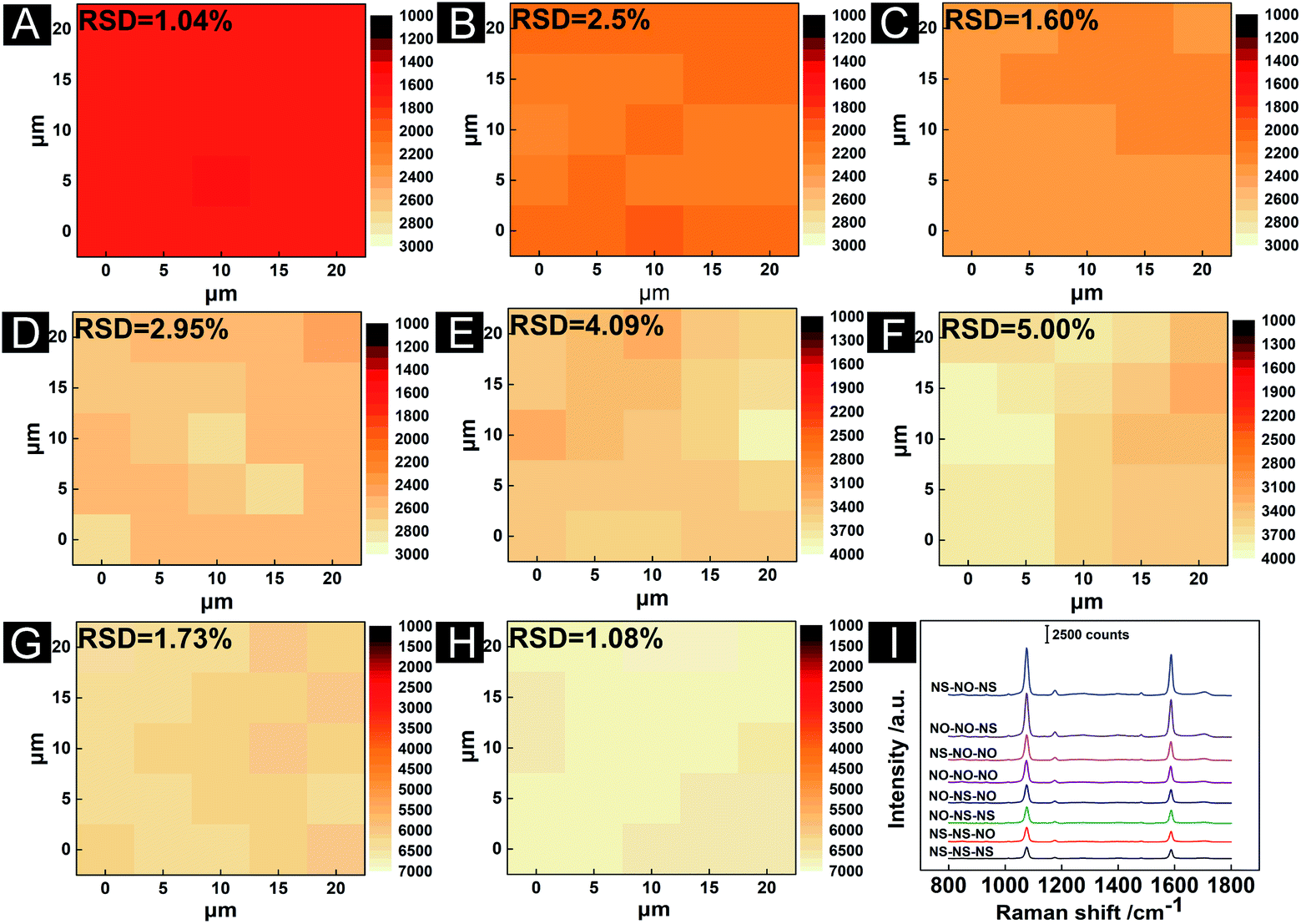 | ||
| Fig. 5 SERS mapping images of the intensity at 1080 cm−1 of 4-MBA with (A) AuNS/AuNS/AuNS, (B) AuNS/AuNS/AuNO, (C) AuNO/AuNS/AuNS, (D) AuNO/AuNS/AuNO, (E) AuNS/AuNO/AuNO, (F) AuNS/AuNO/AuNO, (G) AuNO/AuNO/AuNS, (H) AuNS/AuNO/AuNS. (I) SERS spectra of 4-MBA detected by substrates with different combinations. | ||
3.3 SERS quantitative for molecules
To verify the practicability of the AuNS/AuNO/AuNS 3D hybrid SERS substrate, thiram and MG were employed as the quantitative detection method. Thiram is a fungicide that has been frequently used to prevent fungal disease in seeds and crops. However, with moderate toxicity, it may cause headaches, dizziness, nausea and other gastrointestinal problems for the human to contact thiram suddenly. MG is often used in the aquaculture industry because it is cheap and highly effective. However, it has long been known to be toxic and carcinogenic so to be banned or set the minimum concentrations as low as 2 μg kg−1 in some countries. The detection results of thiram and MG by our optimized 3D substrates were shown in Fig. 6. In the SERS spectra of thiram (Fig. 6A), the peak at 1386 cm−1 was the most obvious that was assigned to asymmetric CH3 deformation mode and C–N stretching mode. Hence, the most distinct peak of thiram at 1386 cm−1 was used for the quantitative analysis. As shown in Fig. 6B, the fitting curve revealed a good linear relationship between the concentration of thiram and the intensity of the SERS intensity of the target peak. The concentration of thiram that the AuNS/AuNO/AuNS 3D hybrid SERS substrate could detect was at least 100 ppb, which was lower than the maximum residual limit of thiram in fruit as required (5 ppm stipulated by China's national standard, 7 ppm and 3 ppm stipulated by the US Environmental Protection Agency and the European Union, respectively). Fig. 6C showed SERS spectra for MG with different concentrations on 3D substrate (AuNS/AuNO/AuNS), which contains the strongest peak at 1617 cm−1 caused by the in-plane vibrations of C–C, and the second strongest peak at 1180 cm−1 assigned by the in-plane modes of C–H bend. With the increase of concentration from 10 nM to 10 μM, the SERS intensity of peak at 1617 cm−1 became stronger with good linearity (R2 of 0.987 in Fig. 6D), showing the potential of this 3D hybrid substrates. Therefore, our substrates were expected to play a practical role in the molecular detection of food and the environment.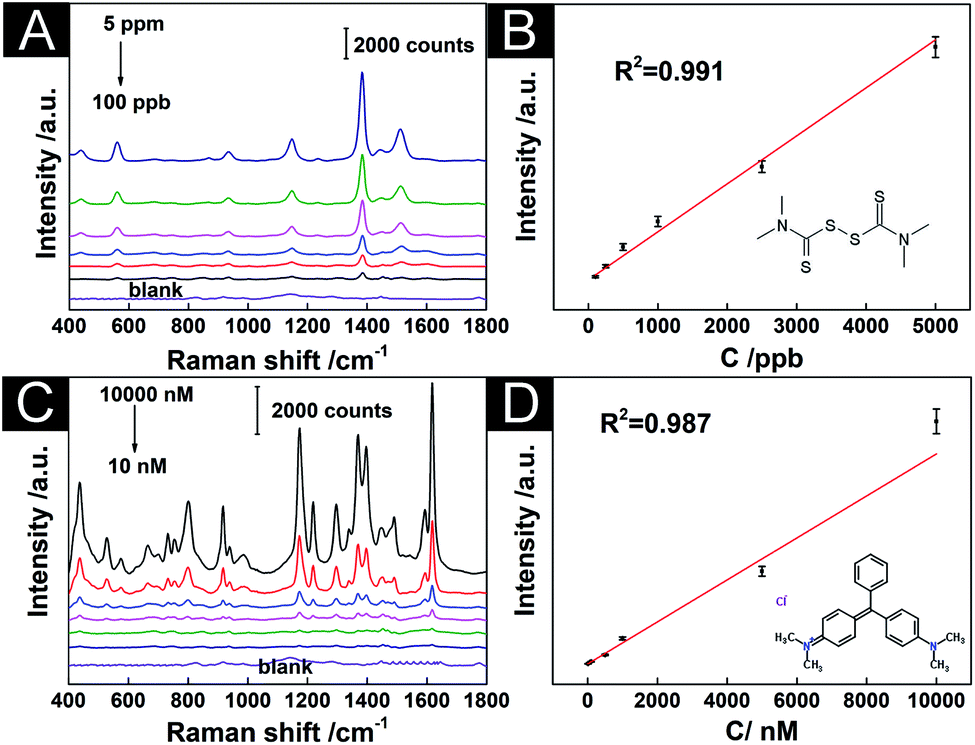 | ||
| Fig. 6 (A) SERS spectra of thiram of different concentrations ranging from 100 to 5000 ppb absorbed on the 3D hybrid SERS substrate (AuNS/AuNO/AuNS). (B) Intensity of 1386 cm−1 as a function of the concentrations of thiram. (C) SERS spectra of MG of different concentrations ranging from 10 nM to 10 μM absorbed on the 3D hybrid SERS substrate (AuNS/AuNO/AuNS). (D) 1617 cm−1 band intensities versus the concentration of MG. Detection condition: laser wavelength 633 nm, accumulation time 1 s, exposure time 1 s and laser power 0.44 mW. | ||
4. Conclusions
In summary, we fabricated highly sensitive and uniform 3D hybrid SERS substrates using an air–liquid interface-assisted self-assembly method to assemble monolayer films closely arranged by AuNO or AuNS nanoparticles onto a substrate. To compare the relationship between the diameter of the Au nanospheres and the SERS enhancement effect, 4-MBA was chosen as the Raman probe molecule. To construct 3D structures, the AuNS with the best SERS activity and the AuNO were selected. The SERS enhancement effects of different combination methods were compared, and the AuNS/AuNO/AuNS showed the best SERS enhancement effect, which also had perfect reproducibility (RSD as low as 1.08%). Furthermore, the detection of small molecules like thiram and MG by AuNS/AuNO/AuNS has shown a good linear relationship, further verifying the substrate's practicality. Through this work, the potential of the hybrid assembly of nanoparticles is further confirmed, which brings a positive sign for developing three-dimensional substrates and the research of plasmonic coupling in the future and provides the availability of molecular detection in the practical application of SERS at the same time.Conflicts of interest
There are no conflicts to declare.Acknowledgements
This work was supported by Xiamen Science and Technology Plan Project (No. 3502Z20193079, 3502Z20203086, 3502Z20203084, 3502Z20191015), the Project of Major Science Technology Innovation Platform of Xiamen (No. 3502ZCQ20171002).References
- D. L. Jeanmaire and R. V. Duyne, J. Electroanal. Chem., 1977, 84, 1–20 CrossRef CAS.
- K. A. Willets and R. V. Duyne, Annu. Rev. Phys. Chem., 2007, 58, 267–297 CrossRef CAS PubMed.
- J. A. Creighton, C. G. Blatchford and M. G. Albrecht, J. Chem. Soc., Faraday Trans. 2, 1979, 75, 790–798 RSC.
- C. Shu, L. Y. Meng, H. Y. Shan, J. F. Li and Z. Q. Tian, ACS Nano, 2016, 10, 581–587 CrossRef PubMed.
- S. Nie and S. R. Emory, Science, 1997, 275, 1102–1106 CrossRef CAS PubMed.
- M. S. Bakshi, G. Kaur, P. Thakur, T. S. Banipal, F. Possmayer and N. O. Petersen, J. Phys. Chem. C, 2007, 111, 5932–5940 CrossRef CAS.
- C. S. Ah, Y. J. Yun, H. J. Park, W. J. Kim, D. H. Ha and W. S. Yun, Chem. Mater., 2011, 17, 5558–5561 CrossRef.
- I. Haas, S. Shanmugam and A. Gedanken, J. Phys. Chem. B, 2006, 110, 16947–16952 CrossRef CAS PubMed.
- K. Taewook, H. Soongweon, C. Yeonho and P. L. Luke, Small, 2010, 3, 66–72 Search PubMed.
- W. Wu, L. Liu, Z. G. Dai, J. H. Liu, S. L. Yang, L. Zhou, X. H. Xiao, C. Z. Jiang and V. A. L. Roy, Sci. Rep., 2015, 5, 12205 CrossRef CAS PubMed.
- R. H. Que, M. W. Shao, S. J. Zhuo, C. Y. Wen, S. D. Wang and S. T. Lee, Adv. Funct. Mater., 2011, 21, 3337–3343 CrossRef CAS.
- H. Liu, L. Yang and J. Liu, Trends Anal. Chem., 2016, 80, 364–372 CrossRef CAS.
- G. C. Phan-Quang, X. Han, C. S. L. Koh, H. Y. F. Sim and X. Y. Ling, Acc. Chem. Res., 2019, 52, 1844–1854 CrossRef CAS PubMed.
- H. M. Lin, Y. H. Chen and S. Gwo, JACS Au, 2010, 132, 11259–11263 CrossRef PubMed.
- E. Chowdhury, M. S. Rahaman, N. Sathitsuksanoh, C. A. Grapperhaus and M. G. O'Toole, Nanotechnology, 2021, 32, 025506 CrossRef CAS PubMed.
- Y. Zeng, F. Wang, D. Du, S. Liu, C. Wang, Z. Xu and H. Wang, Appl. Surf. Sci., 2021, 544, 148924 CrossRef CAS.
- K. Güngr, E. Ünal and H. V. Demir, Opt. Express, 2013, 21, 23097–23106 CrossRef PubMed.
- T. X. Gong, Y. F. Huang, Z. J. Wei, W. Huang, X. B. Wei and X. S. Zhang, Nanotechnology, 2020, 31, 205501 CrossRef CAS PubMed.
- Y. Han, S. Wu, X.-D. Tian and Y. Zhang, ACS Appl. Mater. Interfaces, 2020, 12, 28965–28974 CAS.
- S.-Y. Liu, X.-D. Tian, Y. Zhang and J.-F. Li, Anal. Chem., 2018, 90, 7275–7282 CrossRef CAS PubMed.
- N. Hussain, H. Pu and D. W. Sun, Food Chem., 2021, 350, 129025 CrossRef CAS PubMed.
- Y. Zhang, H. Wu, Z. Liu, S. Xie and J. Li, J. Materiomics, 2021, 7, 347–354 CrossRef.
- H. L. Lai, S. Ghosh and S. Chattopadhyay, Analyst, 2021, 146, 3557–3567 RSC.
- K. Abid, N. H. Belkhir, S. B. Jaber, R. Zribi, M. G. Donato, G. Di Marco, P. G. Gucciardi, G. Neri and R. Maalej, J. Phys. Chem. C, 2020, 124, 20350–20358 CrossRef CAS.
- J. B. Phyo, A. Woo, H. J. Yu, K. Lim, B. H. Cho, H. S. Jung and M. Y. Lee, Anal. Chem., 2021, 93, 3778–3785 CrossRef CAS PubMed.
- J. Liu, C. Zhu, Q. Pan, G. Meng and Y. Lei, ChemistrySelect, 2020, 5, 8338–8343 CrossRef CAS.
- Y. S. Song, H. C. Huang, W. H. Lu, N. L. Li, J. Su, S. B. Cheng, Y. C. Lai, J. Chen and J. H. Zhan, Food Chem., 2021, 344, 128570 CrossRef CAS PubMed.
- Z. Zhan, L. Liu, W. Wang, Z. Cao, A. Martinelli, E. Wang, Y. Cao, J. Chen, A. Yurgens and J. Sun, Adv. Opt. Mater., 2016, 4, 2021–2027 CrossRef CAS.
- J. Reguera, J. Langer, D. Aberasturi and L. Liz-Marzán, Chem. Soc. Rev., 2017, 46, 3866–3885 RSC.
- R. Mei, Y. Wang, Q. Yu, Y. Yin and L. Chen, ACS Appl. Mater. Interfaces, 2020, 12, 2059–2066 CrossRef CAS PubMed.
- Z. Zhu, H. Meng, W. Liu, X. Liu and Z. Tang, Angew. Chem., Int. Ed., 2011, 50, 1593–1596 CrossRef CAS PubMed.
- A. M. Bowen, M. J. Motala, J. M. Lucas, S. Gupta, A. J. Baca, A. Mihi, A. P. Alivisatos, P. V. Braun and R. G. Nuzzo, Adv. Funct. Mater., 2012, 22, 2927–2938 CrossRef CAS.
- Q. Zhang, Y. H. Lee, I. Y. Phang, C. K. Lee and X. Y. Ling, Small, 2014, 10, 2703–2711 CrossRef CAS PubMed.
- S. Yang, M. I. Lapsley, B. Cao, C. Zhao, Y. Zhao, Q. Hao, B. Kiraly, J. Scott, W. Li, L. Wang, Y. Lei and T. J. Huang, Adv. Funct. Mater., 2013, 23, 720–730 CrossRef CAS PubMed.
- Y. Gao, T. You, N. Yang, C. Zhang and P. Yin, Adv. Mater. Interfaces, 2019, 6, 1801966 CrossRef.
- S. Pekdemir, S. Karabel, N. B. Kiremitler, X. Liu, P. F. Nealey and M. S. Onses, ChemPhysChem, 2017, 18, 2114–2122 CrossRef CAS PubMed.
- M. Kahl, E. Voges, S. Kostrewa, C. Viets and W. Hill, Sens. Actuators, B, 1998, 51, 285–291 CrossRef CAS.
- X. Tian, Y. Lin, J. Dong, Y. Zhang, S. Wu, S. Liu, Y. Zhang, J. Li and Z. Tian, Adv. Opt. Mater., 2017, 5, 1700581 CrossRef.
- S. R. Wu, X. D. Tian, S. Y. Liu, Z. Yun and J. F. Li, J. Raman Spectrosc., 2018, 49, 659–667 CrossRef CAS.
- Y. Q. Zheng, Y. Y. Ma, J. Zeng, X. L. Zhong, M. S. Jin, Z. Y. Li and Y. N. Xia, Chem.–Asian J., 2013, 8, 673 CrossRef.
- V. Joseph, A. Matschulat, J. Polte, S. Rolf, F. Emmerling and J. Kneipp, J. Raman Spectrosc., 2011, 42, 1736–1742 CrossRef CAS.
- T. Gong, Y. Luo, H. Zhang, C. Zhao, W. Yue, M. Pu, W. Kong, C. Wang and X. Luo, J. Mater. Chem. C, 2020, 8, 1135–1142 RSC.
- X. Ye, C. Zheng, J. Chen, Y. Gao and C. B. Murray, Nano Lett., 2013, 13, 765–771 CrossRef CAS PubMed.
- M. Richard-Lacroix, Y. Zhang, Z. Dong and V. Deckert, Chem. Soc. Rev., 2017, 46, 3922–3944 RSC.
- Y. Zhang, S. Chen, P. Radjenovic, N. Bodappa, H. Zhang, Z. L. Yang, Z. Tian and J. F. Li, Anal. Chem., 2019, 91, 5316–5322 CrossRef CAS PubMed.
- M. J. Natan, Faraday Discuss., 2006, 132, 321–328 RSC.
- U. S. Dinish, C. Y. Fu, A. Agarwal and M. Olivo, Biosens. Bioelectron., 2011, 26, 1987–1992 CrossRef CAS PubMed.
Footnote |
| † Electronic supplementary information (ESI) available. See DOI: 10.1039/d1ra04473g |
| This journal is © The Royal Society of Chemistry 2021 |