
 Open Access Article
 This Open Access Article is licensed under a Creative Commons Attribution-Non Commercial 3.0 Unported Licence
Realizing new designs of multiplexed electrode chips by 3-D printed masks†
Madeline Keougha,
Jennifer F. McLeodab,
Timothy Salomonsa,
Phillip Hillena,
Yu Peiab,
Graham Gibson ac,
Kevin McEleneya,
Richard Oleschuk*a and
Zhe She*ab
ac,
Kevin McEleneya,
Richard Oleschuk*a and
Zhe She*ab
aDepartment of Chemistry, Queen's University, Chernoff Hall, Kingston, ON K7L 3N6, Canada. E-mail: richard.oleschuk@chem.queensu.ca; zhe.she@queensu.ca
bBeaty Water Research Centre, Queen's University, Kingston, ON K7L 3N6, Canada
cNanoFabrication Kingston, Queen's University, Kingston, ON K7L 0E9, Canada
First published on 17th June 2021
Abstract
Creating small and portable analytical methods is a fast-growing field of research. Devices capable of performing bio-analytical detection are especially desirable with the onset of the global pandemic. Lab-on-a-chip (LOC) technologies, including rapid point-of-care (POC) devices such as glucose sensors, are attractive for applications in resource-poor settings. There are many challenges in creating such devices, from sensitive molecular designs to stable conditions for storing the sensor chips. In this study we have explored using three-dimensional (3D) printing to create shadow masks as a low-cost method to produce multiplexed electrodes by physical vapour deposition. Although the dimensional resolution of the electrodes produced by using 3D printed masks is inferior to those made through photolithography-based techniques, their dimensions can be readily tailored ranging from 1 mm to 3 mm. Multiple mask materials were tested, such as polylactic acid and polyethylene terephthalate glycol, with acrylonitrile butadiene styrene shown to be the best. Simple strategies in making chip holders by 3D printing and controlling working electrode surface area with epoxy glue were also investigated. The prepared chips were tested by performing surface chemistry with thiol-containing molecules and monitoring the signals electrochemically.
Introduction
Developing new and effective diagnostic methods for detection of emerging biological targets has never been more important than during a global pandemic. The need for biological diagnosis does not stop at the detection of deadly viruses, but extends to many other applications, e.g., tracking cancer biomarkers in patients and monitoring bacterial contamination in environmental samples.1 Traditional analysis is reliable, but often time-consuming. For example, after a water sample is transported to a public laboratory, it typically takes 2 to 5 days to generate results for bacterial contaminations.2 In addition, the process requires highly technical personnel to both prepare the samples and perform the analyses. Continuous efforts have been made in an attempt to overcome challenges in development and simplify the analysis. User-friendly point-of-care (POC) devices are goals for many researchers as they can provide rapid on-site diagnosis, which is highly beneficial, particularly in resource-poor settings.3 Emerging methods based on optical, piezoelectric and electrochemical transducers are promising areas of research due to their size, sensitivity, and cost, making them useful for POC methods. Escobedo et al. showed how to combine microfluidic devices with surface plasmon resonance in the detection of uropathogenic Escherichia coli.4 Pingarrón and co-workers reported a piezoelectric method for detecting bacteria using lectin-modified gold sensors.5 Electrochemical sensing, like in the highly successful glucose monitor, has been adapted by Kelley et al. to detect cancer-relevant DNA sequences.6 Furthermore, Kraatz et al. illustrated a new electrochemical and microscopic method to monitor DNA mismatching and perform multiplexed animal species (e.g., chicken, horse and buffalo) recognition.7Electrode designs are critical for effective electrochemical biosensing and the design of the electrode is specified by the application. For instance, Kerman et al. designed tattoo-based potentiometric ion-selective sensors for wearable pH monitoring.8 Kelley et al. have shown that electrochemically deposited nanostructures can enhance sensitivity in biomolecular detection.9 Additionally, White et al. produced aptamer-based sensors on a gold microelectrode platform for absorption of serum proteins.10 There is a multitude of ways to fabricate electrodes with different dimensions and shapes. Electron-beam lithography and chemical etching are highly effective in designing well-defined shapes down to the 30 nm scale.11 However, electron-beam lithography requires an electron-beam source that can be programmed to write the patterns of the electrode, a time-consuming process that is not always readily available due to instrument availability, and the patterning process is time intensive and thus expensive. Alternative electrode fabrication techniques such as photolithography12 and wet or dry etching13,14 are high-resolution techniques for the fabrication of chip electrodes with nanoscale features. However, these methods are not easily accessible, as they are labour-intensive and require access to a clean room.15 Alternatively, soft lithography has also been employed and can be applied easily to create different designs. However, the method is limited by the inability to change designs rapidly.16 Therefore, hybrid methodologies of electron-beam and soft lithographic methods have been developed in making microelectrodes.17
Recently, inkjet printing and screen printing have emerged as useful techniques for printing electrodes because of their ability to rapidly produce patterned conductive materials.18 Wheeler et al. achieved fabrication of a low-cost digital microfluidic device using inkjet printing.19 Dong and co-workers reported using carbon paste to print semi-3D electrodes by layer-by-layer screen printing.20 Mixed Ag–Au nanoparticles and organometallic conductive structure can also be achieved by inkjet printing, reported by Gamerith et al.21 Three-dimensional (3D) printing builds on the inkjet concept but affords the ability to make truly 3D objects with complex architectures via a “layer-by-layer” deposition process. Devices can be designed with computer-assisted drafting software and the 3D models are then sliced into a series of layers for printing. The diversity of the technique has been illustrated in the design of many (bio-)analytical devices, such as sample channels and cartridges.22–24
Printing electrodes with conductive materials directly has its own advantage, but not all electrode materials can be realized in this way yet. In this study, we investigate an alternative method combining 3D printing with physical vapour deposition (PVD) for creating functional chips with gold electrodes (shown schematically in Fig. 1). Functionalized gold surfaces have a wide range of applications in nanotechnology and biosensing.25,26 Self-assembled monolayers, and more specifically, functionalized SAMs, play a central role in applications of gold surfaces.27 3D printing allows for modular mask design, rapid fabrication for various electrode configurations and fabrication of a chip reader to connect the sensor to the analytical instrument. Electrodes can then be produced efficiently with the various mask designs using PVD. However, selecting suitable materials for making the masks and controlling the gold deposition process to create conductive and functional gold layers/electrodes proved challenging. Typically, fused deposition modelling (FDM) 3D printing “ink” materials are intended to have low glass transition temperature (Tg) for easy application, but this means the masks have poor thermal stability for PVD. Searching for a material with good thermal properties after printing led to ABS (acrylonitrile butadiene styrene) being selected as the most suitable material for making the shadow mask. The higher Tg of ABS reduces the risk of warping during the PVD process. Although printing with ABS is slightly harder than materials such as polylactic acid (PLA) and requires printers with larger temperature ranges, ABS printed masks showed good electrode fidelity while being subjected to the radiation and high temperature of electron-beam evaporation (88–92 °C under the experimental conditions). Electrode fidelity was probed using electrochemical experiments that observed charge transfer changes by the modification with thiol-containing molecules. The surface morphology was scanned by atomic force microscopy.
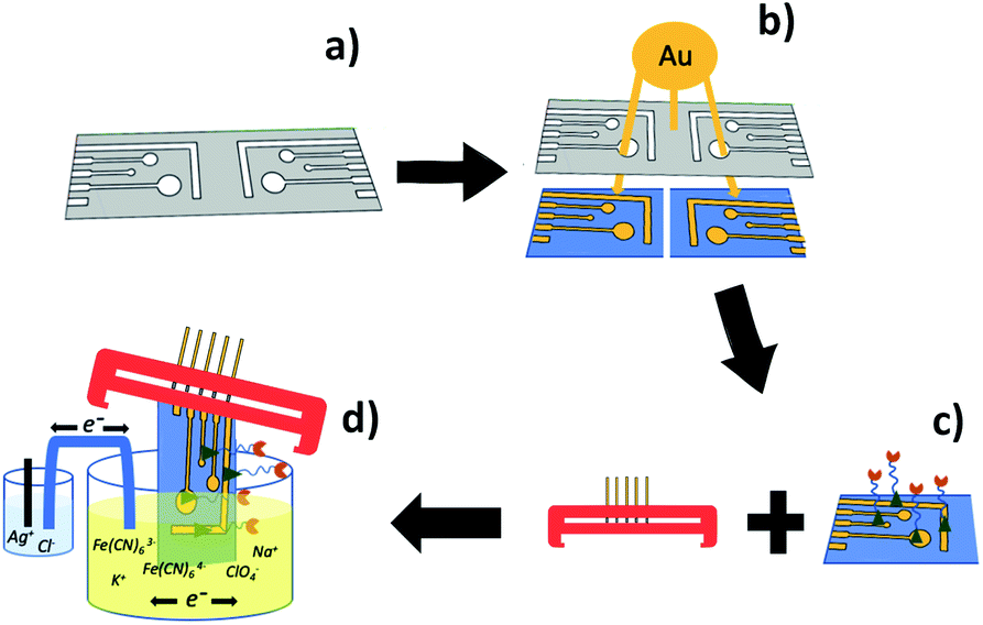 | ||
| Fig. 1 Schematic illustration of fabrication methods and analysis. (a) Photomask fabrication by 3-D printing; (b) electrode fabrication via PVD; (c) surface modification and chip reader fabrication; (d) connecting chip and electrochemical analysis. | ||
Experimental
Reagents
Anhydrous ethyl alcohol was purchased from Greenfield Global (Brampton, Ontario). Acetone (99.5%), potassium nitrate (99%), agar (Fisher BioReagents™), potassium ferrocyanide trihydrate (certified ACS), potassium ferricyanide (certified ACS), HEPES (99%), and sulfuric acid (certified ACS) were purchased from Fisher Scientific (Ottawa, Ontario). Isopropyl alcohol (99%), methanol (99.9%), 6-mercapto-1-hexanol (MCH, 97%), sodium perchlorate monohydrate (98%), and potassium hydroxide (95%) were purchased from Sigma-Aldrich (Oakville, Ontario). PLA filament was purchased from AMZ3D (Amazon.ca). ABS filament was purchased from HatchBox (Pomona, California). Polyethylene terephthalate glycol-modified (PETG) filament was purchased from MG Chemicals (Burlington, Ontario). Gorilla Epoxy™ was obtained from Gorilla Glue Company (Cincinnati, Ohio). Milli-Q (MQ) water (>18.2 MΩ) was used exclusively in the preparation of aqueous solutions.CAD design and 3D printing
The design of shadow masks was completed using two computer-assisted design (CAD) applications, Google SketchUp (Mountain View, California) and OnShape (Cambridge, Massachusetts) (Fig. 2a and b), which are currently available for free. The chip reader design was completed on Fusion 360 by Autodesk, Inc. (San Rafael, California). Designs were exported as .stl files. Shadow mask fabrication methods were optimized for thermal stability and precision. Masks were printed in PLA, PETG and ABS with an Original Prusa i3 MK3S 3D printer by Prusa Research (Prague, Czech Republic). Chip reader structural components, namely the housing, pin holder, and chip tab (Fig. 2c and d), were printed in PLA with the same printer. Superglue™ was used to secure spring-loaded pogo pins to the pin holder in the desired position. For increased flexibility, pogo pins were soldered to copper wires of length 4.5 cm. Glass electrodes were secured to chip tabs with additional adhesive. Screws/nuts were used to secure the chip housing to the chip tab and electrode.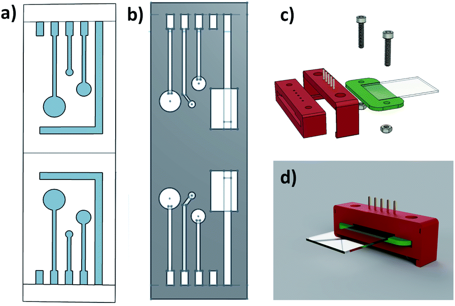 | ||
| Fig. 2 CAD designs for 3D printing. (a) 2D renderings of shadow mask designs for L-shaped counter electrode (CE) from Google SketchUp; (b) block-shaped CE design from OnShape. (c) CAD rendering of chip reader design in exploded view on Fusion 360. (d) CAD rendering of assembled chip reader. Sizes (radii) of working electrodes are 1 mm 2 mm, and 3 mm in both designs. | ||
Electrode fabrication
Electrode fabrication was accomplished at NanoFabrication Kingston (NFK) by depositing gold using electron-beam evaporation, a form of PVD, through a 3D-printed shadow mask onto cleaned standard borosilicate slides. The PVD system contains a 3 kW Linear e-Gun from Thermionics (Hayward, California). Glass slides were cleaned by 30 seconds of rinsing in acetone, isopropyl alcohol (IPA), and deionized water, respectively, with drying under a stream of N2. Organic residue was removed from glass slides by treating them with oxygen plasma using a Plasma-Preen II-973 plasma cleaner from Plasmatic Systems (North Brunswick, New Jersey) operating at 100% power (700 W). Substrates were dehydrated on a baking plate at 200 °C for 5 minutes between plasma cleaning and loading the evaporator to improve metal adhesion. Glass slides and shadow masks were arranged and secured to the plate using single-sided 3 mm-wide Kapton tape. Titanium and gold metals were loaded into separate pockets in the evaporator and were deposited sequentially. Two rounds of depositions (4 glass slides/8 electrode sets) for each condition were carried out. Film thickness was monitored by quartz crystal microbalance. Electrode chips were cleaned by rinsing for 30 seconds under acetone, methanol, and ethanol, respectively, then dried under a stream of N2. Some chips were tested with an additional layer of epoxy coating to cover the contacting wires and control working electrode surface areas. In these cases, equal amounts of Gorilla Epoxy™ resin (Gorilla Glue Company, Cincinnati, Ohio) and hardener were deposited onto a disposable surface and mixed for 60 seconds. Epoxy was applied in the desired area and left to dry for 45 minutes at room temperature.Surface modification
Surface modification was carried out using solutions of 2 mM MCH in EtOH. Filter paper was placed inside a Petri dish and the Au electrode chips were placed on top of the paper. The filter paper was then wetted with 900 μL of the 1![[thin space (1/6-em)]](https://www.rsc.org/images/entities/char_2009.gif) :1 (v/v) MQ/EtOH solution and an aliquot of 50 μL of MCH solution was applied to each working electrode. The Petri dish was carefully sealed with parafilm to prevent evaporation of the liquid droplets. The Petri dish was placed in the refrigerator for 24 hours before an additional 300 μL of 1:1 MQ/EtOH were added to the filter paper and 50 μL of MCH solution applied to each working electrode. This was followed by a further 24 hours in the refrigerator. The Au electrode chips were then rinsed with EtOH for 30 seconds and blown dry with nitrogen gas before electrochemical and surface analysis.
:1 (v/v) MQ/EtOH solution and an aliquot of 50 μL of MCH solution was applied to each working electrode. The Petri dish was carefully sealed with parafilm to prevent evaporation of the liquid droplets. The Petri dish was placed in the refrigerator for 24 hours before an additional 300 μL of 1:1 MQ/EtOH were added to the filter paper and 50 μL of MCH solution applied to each working electrode. This was followed by a further 24 hours in the refrigerator. The Au electrode chips were then rinsed with EtOH for 30 seconds and blown dry with nitrogen gas before electrochemical and surface analysis.
Electrochemical measurements
Electrode chips were cleaned by rinsing with acetone, methanol, and ethanol for 30 seconds, respectively, and then dried under a stream of N2. Organic residue was removed using a plasma etcher for 60 seconds at 1000 mTorr before electrochemistry and surface modifications. Glassware was cleaned by washing with soap and distilled water then rinsing 3–5 times with acetone, 3–5 times with MQ water and dried under a stream of N2. The electrochemical system was set up inside a Faraday cage using an Electrochemical Multiplex Potentiostat (CH Instruments, model CHI1030C). The electrochemical cell is comprised of an external reference electrode (RE, Ag/AgCl in 3 M KCl), three gold working electrodes (WE) and a gold counter electrode (CE) on the glass chip. The electrolyte solution and RE are connected via salt bridge. Following the chip reader assembly, the gold electrode was submerged in electrolyte solution with appropriate electrical connections for each electrode channel. Cyclic voltammograms (CV) were obtained using a window from −0.1 V to 0.6 V with a scan rate of 0.1 V s−1. The scan always started with open-circuit potential and positive scan polarity. Three CV cycles were collected for each set. The 2nd cycles as the first completed cycles are plotted. The sensitivity of the measurement was adjusted to match the current levels.Atomic force microscopy (AFM)
Atomic force microscopy was performed for topographical analysis of bare Au, and Au after SAM formation with MCH. Surface analysis was carried out with an MFP-3D Origins + AFM from Asylum Research, Oxford Instruments (Santa Barbara, California) using an AC160TS-R3 cantilever with resonance frequency of 300 kHz and a spring constant of 26 N m−1. Image processing and data analysis were performed using Gwyddion 2.55 software by the Czech Metrology Institute (Jihlava, Czechia).Results and discussion
Fabrication using advanced techniques such as electron-beam lithography can produce well defined nanostructures and electrodes, offering flexibility in both dimensions and shapes.11 However, electron-beam sources are not readily available. In search of a new flexible design and fabrication process, we have investigated the combination of 3D printing with physical vapour deposition. 3D printing allows one to design features on shadow masks with different sizes and shapes as shown in Fig. 2a and b. Complex architectures containing 3 different working electrodes (radii: 1 mm 2 mm, and 3 mm) have been incorporated into the mask designs. Shadow masks with the L-shaped CE design shown in Fig. 2a were limited by lifting at the corner of the L in the following metal deposition step so the design was modified to a rectangle to improve the mask stability. The surface area of counter electrodes is larger than the surface area of working electrodes. The electrochemical behaviour of the electrodes was tested using a standard external Ag/AgCl reference electrode, although one of the working electrodes could also act as a gold pseudo-reference electrode.Shadow masks were printed from commercially available PLA, ABS, or PETG. ABS, a strong thermoplastic for material extrusion printing,28 has the highest glass transition temperature of the polymers (Table 1) and demonstrated the highest degree of thermal stability during metal depositions. Thermal stability is a crucial factor to be considered for the 3D printed shadow mask due to exposure to radiation during the e-beam evaporation process. Results of four metal depositions and details are shown in Fig. 3. As shown in Fig. 3a and b, masks prepared from PLA and ABS/PETG did not maintain their shapes well during the deposition and the structure of the electrodes on their chips was deformed with bends of approximately 2 to 10 mm. It can be seen that the 2.0 mm ABS masks (Fig. 3c and d) yielded the best results. Even though there is a loss in deposition precision by increasing mask thickness, it is offset by the improved thermal stability of the mask. PVD using ABS masks with thickness of 2 mm was first carried out to deposit 50 nm thickness of gold for the electrode structures to limit the time the mask was exposed to heat. Some of the masks deformed slightly under the conditions, but the electrodes were well defined on the chips. However, the 50 nm thickness of gold was found to be insufficiently conductive. The gold coating thickness was increased to 100 nm to improve conductivity and the ABS masks maintained their shape during the prolonged deposition process. Some ABS masks survived 100 nm deposition better than the 50 nm deposition with little deformation. The exact reason is unknown, but it is speculated it is possibly due to the slight variations in co-polymer composition of acrylonitrile, butadiene and styrene associated with ABS filament. The composition is usually not released by the commercial suppliers. The resolution of the design is influenced by the printer and its nozzle dimensions. The Prusa i3 used in this experiment is very affordable was fitted with a 400 μm diameter nozzle. This can be reduced to produce finer structures with more expensive printers. The smallest feature, the connector, has a width of 1 mm in design in this work. The height of the 3D mask is likely affecting the final dimension, as the fabricated connector was found to be 13 ± 5% (n = 8) smaller than the design (1 mm). The optimized chips from Table 1 condition were used for subsequent electrochemical characterization.
| (a) | (b) | (c) | (d) | |
|---|---|---|---|---|
| Shadow mask material | PLA | PETG/ABS | ABS | ABS |
| Shadow mask thickness (mm) | 0.5/1.0 | 0.5 | 2.0 | 2.0 |
| Adhesive layer | Cr | Ti | Ti | Ti |
| Gold thickness (nm) | 100 | 78 | 50 | 100 |
| Shadow mask Tg (°C) | 60–70 | 70–80/110 | 110 | 110 |
| Mask stability | Low | Very low | Medium | Medium |
| Electrical conductivity | Good | Poor | Very poor | Good |
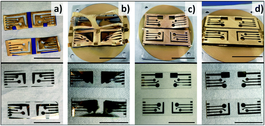 | ||
| Fig. 3 Illustration of masks and chips after physical vapour deposition. Gold was deposited through fused filament 3D printed shadow masks onto standard borosilicate glass slides. (a) 0.5/1.0 mm PLA masks, Cr adhesive layer, 100 nm Au, (b) 0.5 mm ABS/PETG, Ti adhesive layer, 78 nm Au, (c) 2.0 mm ABS, Ti adhesive layer, 50 nm Au (d) 2.0 mm ABS, Ti adhesive layer, 100 nm Au. Scale bars = 4 cm. | ||
Chip readers are essential for making the electrical connections to a potentiostat. Pogo pins incorporated into the chip reader are connected to the leads of the potentiostat, while the electrodes have been designed with connecting pads for the chip reader pins. Chip readers, as shown in Fig. 2c and d, were 3D printed for flexible design, low-cost production, and rapid prototyping. PLA filaments offered good tensile strength for the chip reader and attachment clips with high surface quality.28 Damage to the electrode contact pads occurs when the chip slides into the reader from the pogo pin scratching the gold. To increase the longevity of the electrode and minimize the damage, the chip reader was designed in three pieces (Fig. 2c). The electrodes are fitted into the position with two pieces before the piece with pogo pins is gently clipped to the connecting pads as shown in Fig. S1.†
As SAM formation is an essential step of many applications, we have examined SAMs formed on the gold electrodes prepared using ABS masks and PVD (Table 1). Since SAMs can alter the heterogenous charge transfer between the gold surface and electrolyte solutions,29,30 cyclic voltammetry was used to monitor the formation of the SAMs and changes to the surface as illustrated in Fig. 4a. Cyclic voltammograms were measured on the three working electrodes, small (Fig. 4b), medium (Fig. 4c), and large (Fig. 4d) before and after exposing the gold electrodes to MCH.
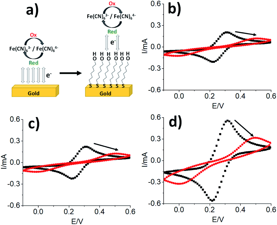 | ||
| Fig. 4 Formation of MCH monolayer on gold electrode surfaces. (a) Illustration of electron transfer before and after MCH modification on gold surfaces. Cyclic voltammograms measured of gold surfaces (black) and gold surface modified with MCH (red) on (b) small WE, (c) medium WE, (d) large WE. The CV was obtained using a scan rate of 0.1 V s−1 in a 10 mM HEPES aqueous buffer pH 7.4 containing 5 mM K4Fe(CN)63−/5 mM K3Fe(CN)64− as a redox couple and 1 M NaClO4 as the supporting electrolyte. RE is a Ag/AgCl/3 M KCl electrode. | ||
For the small gold electrode, a peak separation of 84 mV and an oxidation peak of 0.21 mA at about 0.3 V was observed without functionalization. When the electrode was modified with MCH molecules, an increase in peak separation to 514 mV was observed and the oxidation peak shifted to 0.5 V with a decreased current of 0.12 mA. Similar perturbations were also observed with the medium and large gold electrodes as shown in Fig. 4c and d. The oxidation-reduction peak separations increased from 84 mV to 521 mV and from 102 mV to 489 mV on the medium and large electrodes, respectively. Furthermore, the oxidation and reduction currents were also supressed in the SAM-functionalized electrodes. E.g., oxidation current reduced from 0.22 mA to 0.13 mA for the medium electrode. As expected, formation of a MCH SAM partially blocks the electron transfer between the Fe(CN)63−/4− redox couple and the Au electrode causing the decrease in the oxidation and reduction current leading to the flattening of the curves.
The electron transfer reaction, and the electrode's suitability as a sensor, will be dependent on the morphology of the SAM layer. Thus, the topography of fabricated electrodes was probed by AFM. Fig. 5a and b show the deposited electrode gold surface with thicknesses of 50 and 100 nm, respectively. The 50 nm gold film (Fig. 5a) has more isolated seed crystals compared to the 100 nm gold surface (Fig. 5b) and an increasing amount of grain boundaries. This may lead to the reduced conductivity of the electrode discussed earlier. It is also possible that the non-uniformity of the gold film becomes more pronounced with a thin gold layer of 50 nm. Fig. 5c shows the electrode after MCH modification, and there is no visual difference. Statistical analysis performed on images with consistent dimensions (1 μm × 1 μm, Fig. 5d) illustrates little average height change between the 50 and 100 nm films, with overlapping height distributions. Moreover, the roughness increased insignificantly from a root-mean-square of 1.439 nm to 1.472 nm. More dramatic changes were observed when the surface of the gold electrode was modified with MCH molecules. The surface roughness with a root-mean-square value of 2.174 nm was obtained. More detailed statistical analysis shown in Fig. 5d shows a wider and higher height distribution with MCH-modified gold than the bare gold electrode. This surface change is due to known corrosion effects triggered by the thiol molecules during SAM formation,31 and demonstrates that the deposited gold surface can be functionalized by SAMs, consistent with the electrode's electrochemical changes after the MCH modification.
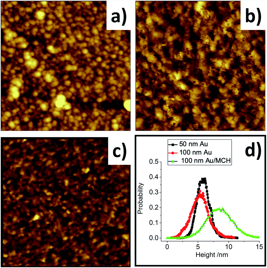 | ||
| Fig. 5 AFM topography images (1 × 1 μm2) of Au surfaces with 5 nm Ti adhesive layer acquired with MFP-3D infinity contact-mode. (a) Bare Au 50 nm thick; (b) bare Au 100 nm thick; (c) MCH/Au 100 nm thick; (d) height distributions of surfaces from topographic image (a) black; (b) red; (c) green. | ||
One challenge in using the electrodes deposited on the chips is controlling the surface area of the working electrodes exposed to the solution. As both the WE and connector are made of gold, the immersion depth of the chip in the solution can vary and this leads to variation in the signals as shown in Fig. 6a, c and e. In order to increase the consistency in the surface area of electrodes, the connectors were coated. Epoxy resin was used as a surface coating as it is robust in aqueous solutions at different pH values and temperatures, and prevents unwanted electrochemical reactions on the covered surfaces.32 Once the connectors between WEs and contact pads are covered, the reproducibility of the CVs and electrode surface area significantly improved as shown in Fig. 6b, d and f. Using the oxidation peak to compare variation of signals, the relative standard deviation of the oxidation peak current before coating the connectors was 11.4%, 12.7% and 5.5% for small, medium and large electrodes (Table 2). Upon epoxy coating, these were reduced to 4.8%, 4.7% and 0.5% respectively. While applying epoxy coating manually does not produce electrodes with perfectly equal surface areas, it does significantly improve the consistency, to as little as 0.5% relative standard deviation for the large electrodes.
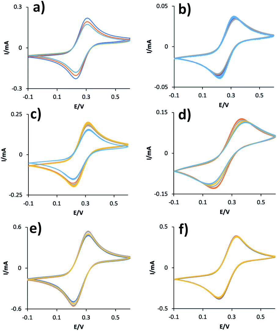 | ||
| Fig. 6 CVs obtained using electrodes with and without epoxy coating on the connectors. No epoxy coating on the connectors of (a) small, (c) medium and (e) large electrodes. Connectors of (b) small, (d) medium and (f) large electrodes are coated with epoxy. The CV was obtained using a scan rate of 0.1 V s−1 in a 10 mM HEPES aqueous buffer containing 5 mM K4Fe(CN)63−/5 mM K3Fe(CN)64− as a redox couple and 1 M NaClO4 as the supporting electrolyte. RE is a Ag/AgCl/3 M KCl electrode. | ||
| Mean oxidation peak (mA) | Standard deviation (mA) | Relative standard deviation (%) | |
|---|---|---|---|
| Small bare | 0.1900 | 0.022 | 11.4 |
| Small epoxy | 0.0352 | 0.002 | 4.8 |
| Medium bare | 0.1914 | 0.024 | 12.7 |
| Medium epoxy | 0.1204 | 0.006 | 4.7 |
| Large bare | 0.5159 | 0.028 | 5.5 |
| Large epoxy | 0.3895 | 0.002 | 0.5 |
Conclusion
We have illustrated the use of 3D printed shadow masks for the fabrication of PVD gold electrodes. Balancing the contrary requirement of lower glass transition temperature for printing material and high temperature stability for PVD, ABS was found to be the best for translating design patterns to functional gold electrodes on chips. Electrode fabrication is also complemented with 3D printed connectors and connecting wire passivation strategies to improve reliability and reproducibility of the devices. Cyclic voltammetry demonstrated the electrodes are electrically active and thiol-gold chemistry can be easily performed on the gold electrodes, opening applications in biosensing and electrocatalysis.33–35 3-D printing is a complementary technique to other shadow mask fabrication methods. Patterning methods such as laser micromachining and xurography can offer finer resolution 1 to 10 μm (ref. 36–38) compared to 3-D printing resolution offered by current FDM printers (50 to 400 μm). However, vinyl films often used by xurography can begin warping with temperatures > 60–100 °C depending on the nature of the of the materials, which limit the fabrication conditions for physical vapour deposition of gold electrodes. Furthermore, FDM 3D printers (similar to that used in this study) cost $300–1000 CAD and are becoming ubiquitous. In contrast, laser machining is much more expensive and not as widely available. These methods are complementary in micro- and nanofabrication applications.Conflicts of interest
There are no conflicts to declare.Acknowledgements
ZS and RO would like to acknowledge Natural Sciences and Engineering Research Council, Canada Foundation for Innovation, Queen's University for their financial supports.References
- S. Vigneshvar, C. C. Sudhakumari, B. Senthilkumaran and H. Prakash, Front. Bioeng. Biotechnol., 2016, 4, 11 CrossRef CAS PubMed.
- Public Health Inspector's Guide to Environmental Microbiology Laboratory Testing, Ontario Agency for Health Protection and Promotion (Public Health Ontario), 2019 Search PubMed.
- S. Kuss, H. M. A. Amin and R. G. Compton, Chem.–Asian J., 2018, 13, 2758–2769 CrossRef CAS PubMed.
- J. Gomez-Cruz, S. Nair, A. Manjarrez-Hernandez, S. Gavilanes-Parra, G. Ascanio and C. Escobedo, Biosens. Bioelectron., 2018, 106, 105–110 CrossRef CAS PubMed.
- B. Serra, M. Gamella, A. J. Reviejo and J. M. Pingarrón, Anal. Bioanal. Chem., 2008, 391, 1853–1860 CrossRef CAS PubMed.
- J. Das, I. Ivanov, T. S. Safaei, E. H. Sargent and S. O. Kelley, Angew. Chem., 2018, 130, 3773–3778 CrossRef.
- P. M. Diakowski and H. B. Kraatz, Chem. Commun., 2011, 47, 1431–1433 RSC.
- A. J. Bandodkar, V. W. S. Hung, W. Jia, G. Valdés-Ramírez, J. R. Windmiller, A. G. Martinez, J. Ramírez, G. Chan, K. Kerman and J. Wang, Analyst, 2013, 138, 123–128 RSC.
- B. Lam, J. Das, R. D. Holmes, L. Live, A. Sage, E. H. Sargent and S. O. Kelley, Nat. Commun., 2013, 4, 2001 CrossRef PubMed.
- J. Liu, S. Wagan, M. Dávila Morris, J. Taylor and R. J. White, Anal. Chem., 2014, 86, 11417–11424 CrossRef CAS PubMed.
- C. Vieu, F. Carcenac, A. Pépin, Y. Chen, M. Mejias, A. Lebib, L. Manin-Ferlazzo, L. Couraud and H. Launois, Appl. Surf. Sci., 2000, 164, 111–117 CrossRef CAS.
- M. Debono, D. Voicu, M. Pousti, M. Safdar, R. Young, E. Kumacheva and J. Greener, Sensors, 2016, 16, 2023 CrossRef PubMed.
- N. V. Hoang, S. Kumar and G.-H. Kim, Nanotechnology, 2009, 20, 125607 CrossRef PubMed.
- S. Minnikanti, J. Ahn, Y. S. Obeng and D. R. Reyes, ACS Nano, 2019, 13, 3924–3930 CrossRef CAS PubMed.
- J. Yan, V. A. Pedrosa, A. L. Simonian and A. Revzin, ACS Appl. Mater. Interfaces, 2010, 2, 748–755 CrossRef CAS PubMed.
- L. W. James, K. Amit, A. B. Hans, K. Enoch and M. W. George, Nanotechnology, 1996, 7, 452–457 CrossRef.
- Z. She, A. Di Falco, G. Hahner and M. Buck, Appl. Surf. Sci., 2016, 373, 51–60 CrossRef CAS.
- C. Dixon, J. Lamanna and A. R. Wheeler, Adv. Funct. Mater., 2017, 27, 1604824 CrossRef.
- C. Dixon, A. H. C. Ng, R. Fobel, M. B. Miltenburg and A. R. Wheeler, Lab Chip, 2016, 16, 4560–4568 RSC.
- H. Zhu, X. Lin, Y. Su, H. Dong and J. Wu, Biosens. Bioelectron., 2015, 63, 371–378 CrossRef CAS PubMed.
- S. Gamerith, A. Klug, H. Scheiber, U. Scherf, E. Moderegger and E. J. W. List, Adv. Funct. Mater., 2007, 17, 3111–3118 CrossRef CAS.
- G. I. J. Salentijn, P. E. Oomen, M. Grajewski and E. Verpoorte, Anal. Chem., 2017, 89, 7053–7061 CrossRef CAS PubMed.
- A. V. Nielsen, M. J. Beauchamp, G. P. Nordin and A. T. Woolley, Annu. Rev. Anal. Chem., 2020, 13, 45–65 CrossRef PubMed.
- B. C. Gross, J. L. Erkal, S. Y. Lockwood, C. Chen and D. M. Spence, Anal. Chem., 2014, 86, 3240–3253 CrossRef CAS PubMed.
- J. C. Love, L. A. Estroff, J. K. Kriebel, R. G. Nuzzo and G. M. Whitesides, Chem. Rev., 2005, 105, 1103–1169 CrossRef CAS PubMed.
- N. Wongkaew, M. Simsek, C. Griesche and A. J. Baeumner, Chem. Rev., 2019, 119, 120–194 CrossRef CAS PubMed.
- C. D. Bain, E. B. Troughton, Y. T. Tao, J. Evall, G. M. Whitesides and R. G. Nuzzo, J. Am. Chem. Soc., 1989, 111, 321–335 CrossRef CAS.
- J.-Y. Lee, J. An and C. K. Chua, Appl. Mater. Today, 2017, 7, 120–133 CrossRef.
- A. L. Eckermann, D. J. Feld, J. A. Shaw and T. J. Meade, Coord. Chem. Rev., 2010, 254, 1769–1802 CrossRef CAS PubMed.
- A. L. Eckermann, J. A. Shaw and T. J. Meade, Langmuir, 2010, 26, 2904–2913 CrossRef CAS PubMed.
- K. Edinger, M. Grunze and C. Wöll, Ber. Bunsen-Ges. Phys. Chem., 1997, 101, 1811–1815 CrossRef CAS.
- D. G. Kurth, G. K. Broeker, C. P. Kubiak and T. Bein, Chem. Mater., 1994, 6, 2143–2150 CrossRef CAS.
- M. L. Clark, A. Ge, P. E. Videla, B. Rudshteyn, C. J. Miller, J. Song, V. S. Batista, T. Lian and C. P. Kubiak, J. Am. Chem. Soc., 2018, 140, 17643–17655 CrossRef CAS PubMed.
- J. McLeod, C. Park, A. Cunningham, L. O’Donnell, R. S. Brown, F. Kelly and Z. She, Analyst, 2020, 145, 6024–6031 RSC.
- S. Martic, M. Labib and H. B. Kraatz, Electrochim. Acta, 2011, 56, 10676–10682 CrossRef CAS.
- D. A. Bartholomeusz, R. W. Boutte and J. D. Andrade, J. Microelectromech. Syst., 2005, 14, 1364–1374 Search PubMed.
- J. Liu, J. B. Mahony and P. R. Selvaganapathy, Microsyst. Nanoeng., 2017, 3, 17040 CrossRef CAS PubMed.
- A. Kundu, C. Nattoo, S. Fremgen, S. Springer, T. Ausaf and S. Rajaraman, RSC Adv., 2019, 9, 8949–8963 RSC.
Footnote |
| † Electronic supplementary information (ESI) available. See DOI: 10.1039/d1ra03482k |
| This journal is © The Royal Society of Chemistry 2021 |