DOI:
10.1039/D1RA03438C
(Paper)
RSC Adv., 2021,
11, 19482-19491
Ultra-wideband self-powered photodetector based on suspended reduced graphene oxide with asymmetric metal contacts†
Received
2nd May 2021
, Accepted 19th May 2021
First published on 28th May 2021
Abstract
The ultraviolet to terahertz band forms the main focus of optoelectronics research, while light detection in different bands generally requires the use of different materials and processing methods. However, researchers are aiming to realize multi-band detection simultaneously in the same device in certain specific application scenarios and ultra-wideband photoelectric detectors can also realize multi-function and multi-system integration. Therefore, the research and development work on ultra-wideband photoelectric detectors has important practical application value. Here, we produced self-powered suspended Pd-reduced graphene oxide-Ti (Pd-rGO-Ti) photodetectors. We varied the properties of the rGO films by using different annealing temperatures and achieved p-doping and n-doping of the films by evaporating palladium films and titanium films, respectively, thus enabling preparation of photothermoelectric (PTE) photodetectors based on rGO films. The resulting detectors have excellent photoelectric responses over a wideband illumination wavelength range from 375 nm to 118.8 μm (2.52 THz). At the same time, we determined the best experimental conditions and device structure by varying the channel width, the laser spot irradiation position and the experimental atmospheric pressure. The maximum responsivity obtained from our detectors is 142.08 mV W−1, the response time is approximately 100–200 ms and the devices have high detection sensitivity. Based on this work, we assumed in the subsequent experiments that detectors with higher performance can be obtained by reducing the channel width and atmospheric pressure. With advantages that include simple fabrication, low cost, large-scale production potential and ultra-wideband responses, these Pd-rGO-Ti photodetectors have broad application prospects in high-performance integrated optoelectronics.
1 Introduction
Electromagnetic waves cover the range from gamma rays to radio waves and each wave band in this range is of great value and significance to mankind. Among these wave bands, the ultraviolet to terahertz range represents the main focus of optoelectronics research. This band of light carries a great deal of valuable information. For example, ultraviolet light detection plays an important role in applications including astronomy and environmental monitoring.1–3 In addition, visible light detection is the cornerstone of modern digital camera technology,3–5 while infrared light detection is an important aspect of optical communications and plays an irreplaceable role in health detection, security systems and night vision applications.3,6,7 Terahertz light (0.1–10 THz) is of great value in nondestructive testing and biomedical imaging applications because of the weak photon energies involved.3,8–10 Therefore, the development of an ultra-wideband photoelectric detection system that can detect all wavelengths from ultraviolet to terahertz is highly significant.
Photodetection is a frontier research subject that has seen in-depth development but is still advancing constantly. This research mainly involves studies of the interactions between light and matter and retrospective study of the detected optical information through the changes that occur in the system's electrical parameters, including the amplitude, phase, polarization state and other optical parameters. To date, there have been numerous representative optoelectronic response materials, including the first and second generations of semiconductors, which have reached very mature application stages, and third generation semiconductors with larger bandgap widths.11–17 As a semiconductor material with a direct bandgap, black phosphorus (BP) is used widely in the study of photoelectric responses to visible and near-infrared light.18–20 Transitional metal dichalcogenides (TMDCs) play important roles in the development of high-performance optoelectronic devices.21–23 Because of their excellent photovoltaic characteristics, the potential use of perovskite materials as photoelectric responsive materials has gradually attracted researchers' attention.24,25 In addition to the materials mentioned above, another very important class of photoelectric detection materials is carbon-based nanomaterials. Graphene and graphene-based materials are the most representative examples of carbon-based photoelectric responsive materials.26–31 The zero-bandgap structure of graphene represents not only its most prominent advantage but also an inevitable disadvantage in the development of graphene photoelectric detectors. The advantages lie mainly in the theoretical possibility of full spectral absorption with a zero bandgap, while the disadvantages are that the band electrons have both very short excitation lifetimes and very low quantum efficiency. In addition, monolayer graphene absorbs only 2.3% of the incident light in the infrared and visible spectral range.32,33 These problems mean that graphene is unable to meet the application requirements of high-performance wide spectrum photoelectric detection materials fully. As a superior graphene-based material, reduced graphene oxide (rGO) is therefore attracting increasing attention from researchers.
As a derivative of graphene, rGO is prepared by oxidizing and ultrasonically peeling graphite to produce graphene oxide and then reducing this oxide. The resulting material has rich and tunable photoelectric properties. First, the energy band structure of rGO is adjustable. This adjustability occurs because a portion of the carbon atoms in rGO are bonded with oxygen-containing functional groups, including hydroxyl, epoxy, carbonyl and carboxyl groups; these carbon atoms are thus transformed from the sp2 hybridization to the sp3 hybridization and the sp3 hybridization produces a δ bond, which causes the material to have a wide bandgap. Second, the semiconductor type of rGO can also be adjusted. If electron-extracting functional groups such as the carboxyl, carbonyl, sp3-bonded hydroxyl, ether and epoxide groups in rGO are dominant, the material will be p-type, but if electron-donating functional groups such as the sp2-bonded hydroxyl, ether and epoxide groups are dominant, the material will then be n-type. Therefore, the semiconductor type can be converted between p-type and n-type by simply changing the proportion of functional groups present in the material.34 Finally, the work function of rGO can be adjusted. Molecular dynamics and density functional theory calculations show that the rGO work function can be adjusted significantly by adjusting the type of oxygen-containing functional group used in the material.35 At present, rGO-based photodetectors cover the ultra-wideband spectrum from the ultraviolet (UV) to the mid-infrared (MIR) band.36,37 Basant et al. realized UV light detection using rGO prepared by a solution method and Liang et al. used the high-temperature resistivity of rGO to realize the MIR photoelectric response.38–40 However, two prominent problems are still restricting practical application of these rGO photodetectors. First, the response speeds of these detectors are slow. The reported response times of rGO detectors are generally on the level of seconds or even minutes. The other problem is the low device responsivity, with the rGO detectors reported to date typically having responsivities below 10 mA W−1.38,41–43
In this work, self-powered suspended Pd-rGO-Ti photodetectors that were annealed at various temperatures were fabricated. The self-supporting rGO film was suspended on a hollow substrate to avoid the cooling of photoexcited carriers from substrate surface polar phonons and the heat dissipation from the substrate.44,45 At the same time, self-powered photothermoelectric detectors were realized by evaporating metal layers with different work functions. We determined the best device structure and best experimental conditions by studying the effects of the different test conditions, including the location of the laser spot, the annealing temperature, the channel width between the Pd-plated area and the Ti-plated area, the laser wavelength and the atmospheric pressure, on the performance of our photodetectors. These detectors realize ultra-wideband photoelectric detection from the ultraviolet to the terahertz region simultaneously. The highest responsivity is 142.08 mV W−1 and the response time ranges from approximately 100–200 ms. In addition, the detectors reduce the detection noise considerably without application of an external bias, which allows them to have very high detection sensitivity.
2 Results and discussion
2.1 Preparation and characteristics of the Pd-rGO-Ti photodetectors
The monolayer or multilayer graphene oxide (GO) for use in the experiments was prepared using Hummers' method.46 The prepared GO powder was configured with deionized water in a specific ratio into a 2 mg mL−1 GO aqueous solution and was mixed uniformly via ultrasonic dispersion. The prepared GO solution was then drip-coated on a tailored polytetrafluoroethylene (PTFE) substrate and was stored at room temperature (25 °C) for 72 h to allow the water in the solution to evaporate naturally and thus form a GO film. The extremely low surface energy of PTFE meant that the GO film could be removed from the substrate completely to obtain a self-supporting GO film. The GO film was then placed in a mixed atmosphere composed of 95% argon (Ar) and 5% hydrogen (H2) for heat treatment for 3 h to prepare the reduced graphene oxide (rGO) film. The annealing temperatures used were 200, 400, 600, 800 and 1000 °C. Fig. S1† show scanning electron microscopy (SEM) images of the surfaces of the rGO films that were annealed at the different temperatures. There are no significant differences in the morphologies of the rGO films and the film surfaces all show wrinkles. The cross-sectional images (Fig. S2†) show that the thickness of the films used in the experiment is in the 1–2 μm range.
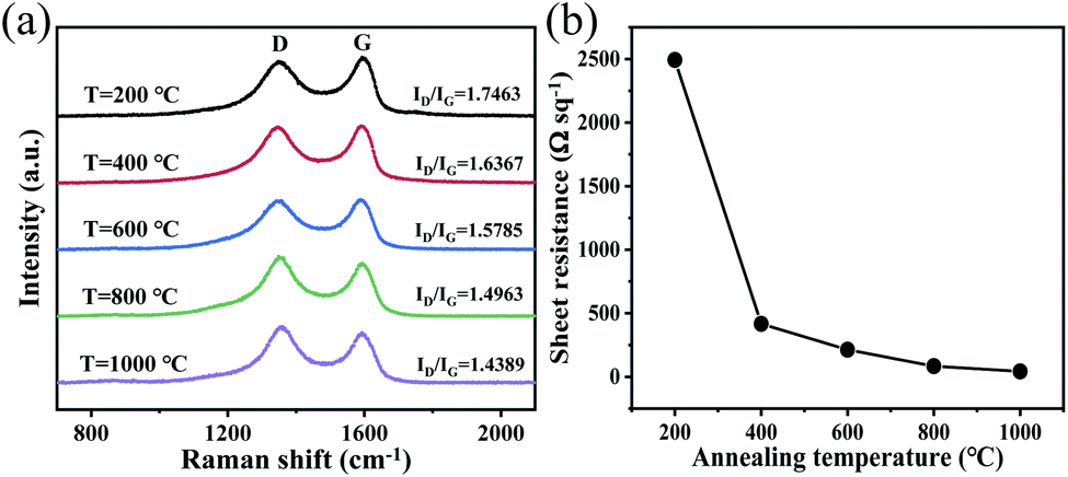
Raman spectroscopy characterizes the effects of the annealing temperature on the internal structures of the rGO films. As shown in Fig. 1a, the films that were prepared at different annealing temperatures show two strong Raman bands at 1351 cm−1 and 1592 cm−1, which correspond to the D band and the G band of graphene, respectively. The ratio of the D band and G band intensities (ID/IG) is associated with the defect concentration in the graphitic carbon materials. As the annealing temperature increases, ID/IG decreases from 1.7463 to 1.4389. This means that the size of each sp2 hybridized region inside the rGO is reduced but the number of sp2 hybridized regions is increased simultaneously and this can improve the conductivity of the films.47–50 The sheet resistance values of the rGO films annealed at the different temperatures are measured using the four probe method and the results are shown in Fig. 1b. The sheet resistance is an important parameter when evaluating the restoration of a π-conjugated system.51 The results indicate that the sheet resistance decreased significantly from 2493.8 Ω sq−1 to 42.7 Ω sq−1 as the annealing temperature rose, i.e., the film conductivity is greatly improved, which demonstrates that high annealing temperatures are beneficial for restoration of π-conjugated systems.52,53
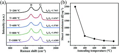 |
| | Fig. 1 (a) Raman spectra and (b) sheet resistances of free-standing rGO thin films that were annealed at 200, 400, 600, 800 and 1000 °C. | |
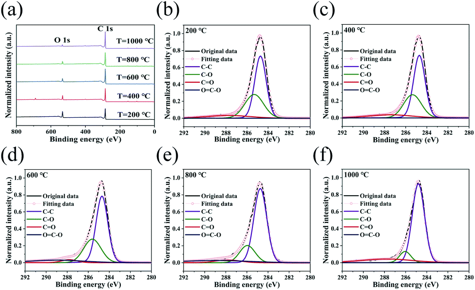
Fig. 2a shows the survey spectra of the rGO films with their different annealing temperatures obtained by X-ray photoelectron spectroscopy (XPS). The peaks at 285 eV and 534 eV represent C 1s and O 1s, respectively. The peak at around 700 eV comes from the Mn element introduced in the Hummers' method used to prepare GO films, and the peaks below 200 eV come from the Si element introduced in the silicon wafer which holds down the GO film in order to prevent it from being removed during vacuum pumping in the annealing process. As the annealing temperature increases, the total oxygen content of the rGO film decreases in tandem; this is then manifested as a reduction in the intensity of the O 1s spectra and an increase in the ratio of C to O. This indicates that a higher annealing temperature produces a higher degree of reduction, more thorough removal of the oxygen from the GO and better film conductivity. The distinct peak at around 700 eV comes from the Mn element introduced in the Hummers' method used to prepare GO films, and the peaks below 200 eV come from the Si element introduced in the silicon substrate used in the annealing process.The C 1s XPS spectra of the rGO films are divided into four functional groups: C–C (∼284.7 eV), C–O (∼285.6 eV), C![[double bond, length as m-dash]](https://www.rsc.org/images/entities/char_e001.gif) O (∼287.8 eV) and OC–O (∼289.0 eV), as shown in Fig. 2b–f. As the reduction temperature increases, the proportion of C–C functional groups in the film also increases while the proportions of the other three oxygen-containing functional groups gradually decrease, thus indicating that increasing the annealing temperature can increase the removal rates of the oxygen-containing functional groups and bring the rGO closer in structure to intrinsic graphene. However, even if the annealing temperature reaches 1000 °C, a small amount of the C–O functional group still remains in the rGO, which means that the rGO cannot be reduced fully to intrinsic graphene.
O (∼287.8 eV) and OC–O (∼289.0 eV), as shown in Fig. 2b–f. As the reduction temperature increases, the proportion of C–C functional groups in the film also increases while the proportions of the other three oxygen-containing functional groups gradually decrease, thus indicating that increasing the annealing temperature can increase the removal rates of the oxygen-containing functional groups and bring the rGO closer in structure to intrinsic graphene. However, even if the annealing temperature reaches 1000 °C, a small amount of the C–O functional group still remains in the rGO, which means that the rGO cannot be reduced fully to intrinsic graphene.
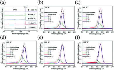 |
| | Fig. 2 (a) Survey XPS spectra of rGO reduced at different temperatures. C 1s XPS spectra of rGO thin films annealed at (b) 200, (c) 400, (d) 600, (e) 800 and (f) 1000 °C. | |
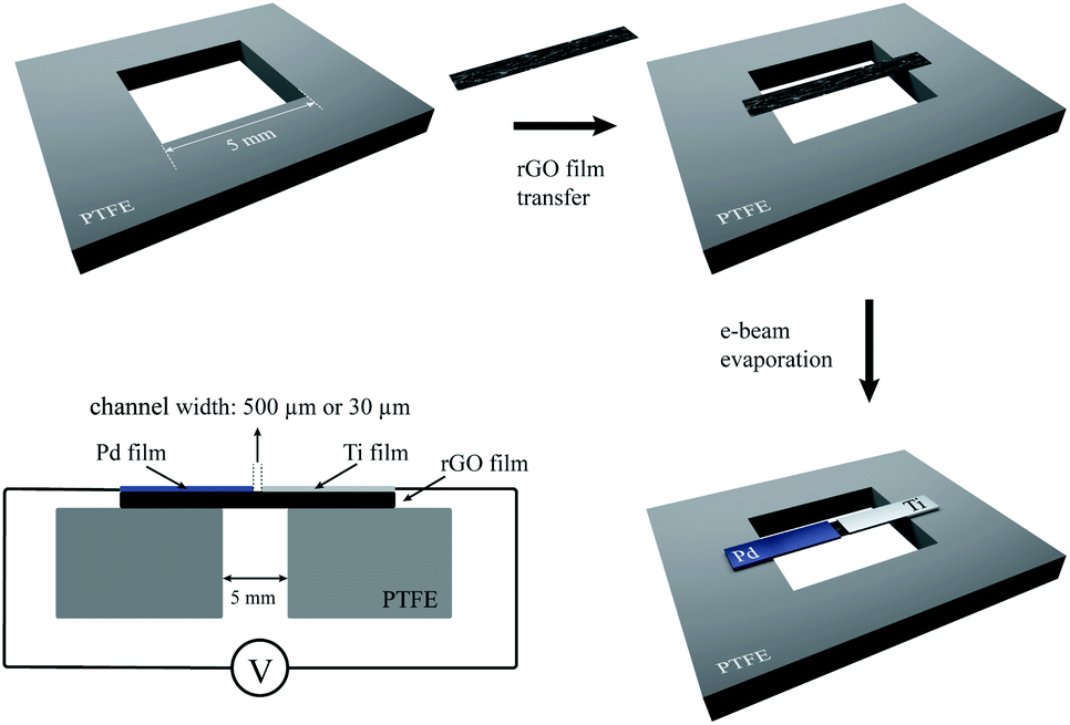
The work function of rGO decreases from 4.9 eV to 4.5 eV with the increase of the annealing temperature.54,55 To achieve good p-type doping and n-type doping to the rGO films, it is necessary to select metals with high work functions and low work functions, respectively. The Fermi level of high work function metal is close to the valence band of rGO, thus forming a Schottky barrier that is large relative to electrons and small relative to holes. Therefore, the barrier is favorable for hole injection and unfavorable for electron injection. At this time, the working current of rGO mainly comes from holes and the device is p-type. In contrast, the Fermi level of low work function metal is close to the conduction band of rGO, thus forming a Schottky barrier that is large relative to holes and small relative to electrons. Therefore, the barrier is favorable for electron injection and the device is n-type. In addition, the selected metals and the rGO must both show good wettability and remain stable in the atmospheric environment. For some high work function metals with good wettability, it can even form a barrier-free contact with the valence band to holes. While for low work function metals with good wettability, it can form a barrier-free contact with the conduction band to electrons.56–61 After consideration of the factors listed above, palladium is selected to form the p-type ohmic contact and titanium is selected to fabricate the n-type ohmic contact to rGO by electron beam vapor deposition. Fig. 3 illustrates the fabrication process used for the suspended Pd-rGO-Ti photodetectors (for further fabrication details, see the Device fabrication section). Fig. S3a† shows the photomicrographs of the Pd-rGO-Ti nanostructures. The region with the evaporated palladium film is shown on the left, the region with the evaporated titanium film is shown on the right, and the rGO intrinsic region is in the middle. The channel width between the two metal electrodes was controlled by adjusting the mask size to research the effects of the channel width on the photodetector performance. In our experiments, two channel widths of 500 μm and 30 μm were selected. Photographs of the photodetectors with the two different channel widths are shown in Fig. S3b and c.†
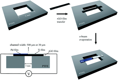 |
| | Fig. 3 Schematic illustration of the fabrication process for the Pd-rGO-Ti photodetectors. The figure on the bottom left shows a diagrammatic cross-section of the photodetector. | |
2.2 Photoresponses of the Pd-rGO-Ti photodetectors under UV to THz illumination
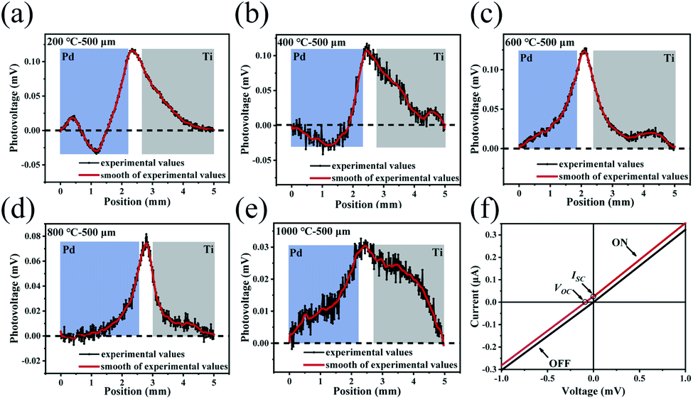
The photoresponse performances of the Pd-rGO-Ti photodetectors were tested using various types of continuous-wave laser, including UV (375 nm), visible (532 nm) and near-infrared (808 and 1550 nm) semiconductor lasers, a middle-infrared (10.6 μm) CO2 laser and a 2.52 THz (118.8 μm) gas laser. Full details of these measurements can be found in the Material characterization and photoelectric measurements section. The results of scanning photovoltage measurements from the palladium-plated area to the titanium-plated area of the photodetectors with 500 μm channel annealed at different temperatures under illumination at 532 nm are shown in Fig. 4a–e. The corresponding scanning measurement results for the detectors with 30 μm channel are shown in Fig. S4a–e.† When the light spot was scanned continuously from the palladium-plated area to the titanium-plated area, the photovoltages of the photodetectors that were annealed at 200 °C and 400 °C changed from negative to positive, while the photodetectors annealed at 600 °C, 800 °C and 1000 °C continued to output positive photovoltages. However, when the light spot irradiated a location of the intrinsic region, the devices that were annealed at the different temperatures all output their maximum photovoltages. Therefore, in subsequent experiments with illumination at different wavelengths, the position with the maximum photovoltage output was selected for detection in all cases. Current–voltage (I–V) characteristics measured with (red line) and without (black line) laser illumination of the photodetector (annealing temperature: 200 °C) are shown in Fig. 4f. Upon illumination of this photodetector, a net photocurrent was generated at zero bias (ISC) along with an open circuit voltage (VOC), which is a typical photothermoelectric (PTE) signature. The absence of any changes in the slope of the I–V curve excluded bolometric effects from being the origin of the photosignal observed here.
 |
| | Fig. 4 Scanning photovoltage measurement results from the palladium-plated area to the titanium-plated area of photodetectors with 500 μm channel annealed at (a) 200, (b) 400, (c) 600, (d) 800 and (e) 1000 °C under illumination at 532 nm. (f) I–V curve of the Pd-rGO-Ti photodetector, annealed at 200 °C, with (red line) and without (black line) laser illumination. | |
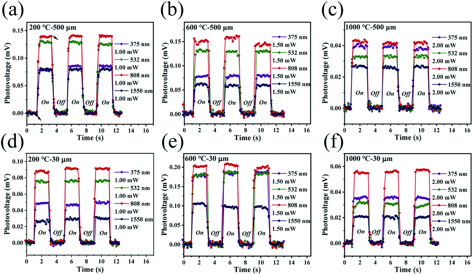
Fig. 5a–f and S5a–d† show the three periods of the photovoltage under UV to near-infrared (NIR) light illumination. The time periods with and without light are both 2 s long. The photovoltage of the detector is zero without illumination but the photovoltage rises rapidly to its maximum value during illumination. When the detector returns to the dark state again, the photovoltage decays rapidly to zero. Multiple on/off cycling demonstrated that our detector can produce a good dynamic response and good stability and reproducibility, and the photoresponse curves recorded at various wavelengths all show the same trend. It should be noted here that the photovoltage fluctuates when the detector is illuminated; these fluctuations are mainly caused by the fact that the suspended rGO film is easily affected by any slight fluctuations in the surrounding air.
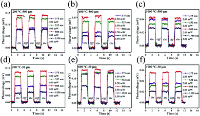 |
| | Fig. 5 On–off curves of the photovoltages of photodetectors annealed at (a) 200, (b) 600 and (c) 1000 °C with the 500 μm channel and annealed at (d) 200, (e) 600 and (f) 1000 °C with the 30 μm channel when illuminated at different light wavelengths under UV to NIR. | |
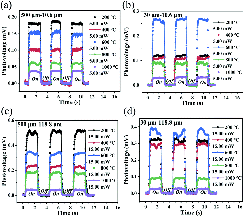
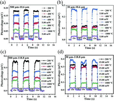
Fig. 6a–d show three periods of the photovoltage for photodetectors with two different channels that were annealed at different temperatures under illumination at 10.6 μm and 2.52 THz. The figures show that the detector also has good stability and reproducibility under middle-infrared (MIR) and terahertz illumination. The photovoltage ΔV generated after illumination was caused by the PTE effect and can be expressed as:
here,
S is the Seebeck coefficient and Δ
T is the temperature rise of the heated area of the device.
3,62 The phenomenon by which the temperature rises after the material absorbs the energy from light irradiation is called the photothermal effect and this temperature difference will cause the voltage to be generated;
i.e., when the electrons (or holes) in the heated material move with the temperature gradient from the high temperature area to the low temperature area, a current will be generated and the potential difference will be formed along with charge accumulation. The Seebeck coefficient is defined as the gradient of the electric potential with respect to the temperature change:
if the semiconductor is n-type, the moving carriers are electrons and the Seebeck coefficient
SN is negative,
i.e.,
SN < 0. However, if the semiconductor is p-type, the holes are the moving carriers and the Seebeck coefficient
SP is positive,
i.e.,
SP > 0. The difference in the photovoltage generated by the photodetectors that were annealed at different temperatures mainly comes from the change in the semiconductor type and the work function of the rGO films caused by the different annealing temperatures, but the quantitative change requires further study.
 |
| | Fig. 6 On–off curves of the photovoltage of the (a) 500 μm wide channel and (b) 30 μm wide channel photodetectors under 10.6 μm illumination. On–off curves of the photovoltage of the (c) 500 μm wide channel and (d) 30 μm wide channel photodetectors under 2.52 THz illumination. | |
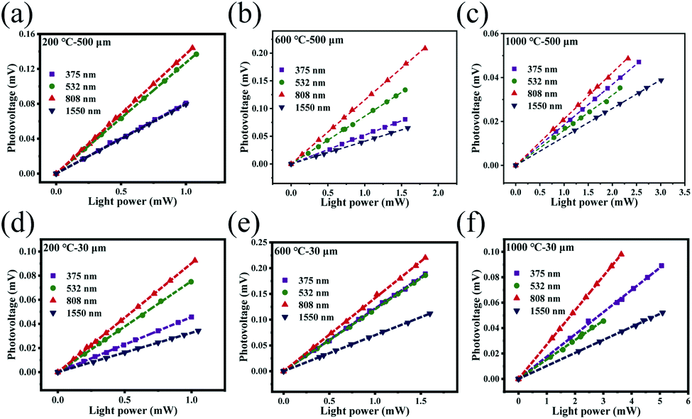
Fig. 7a–e and S6a–d† show the power dependences of the photovoltages of the photodetectors for a series of light wavelengths ranging from the UV to the NIR region. It is obvious from these results that the photovoltage is linearly proportional to the illumination power, which ensures linear behavior in the Pd-rGO-Ti devices that were annealed at different temperatures when operating as photodetectors.
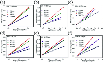 |
| | Fig. 7 Dependence of photovoltage on light power under UV to NIR illumination of detectors with 500 μm wide channels annealed at (a) 200, (b) 600 and (c) 1000 °C and detectors with 30 μm wide channels annealed at (d) 200, (e) 600 and (f) 1000 °C. | |
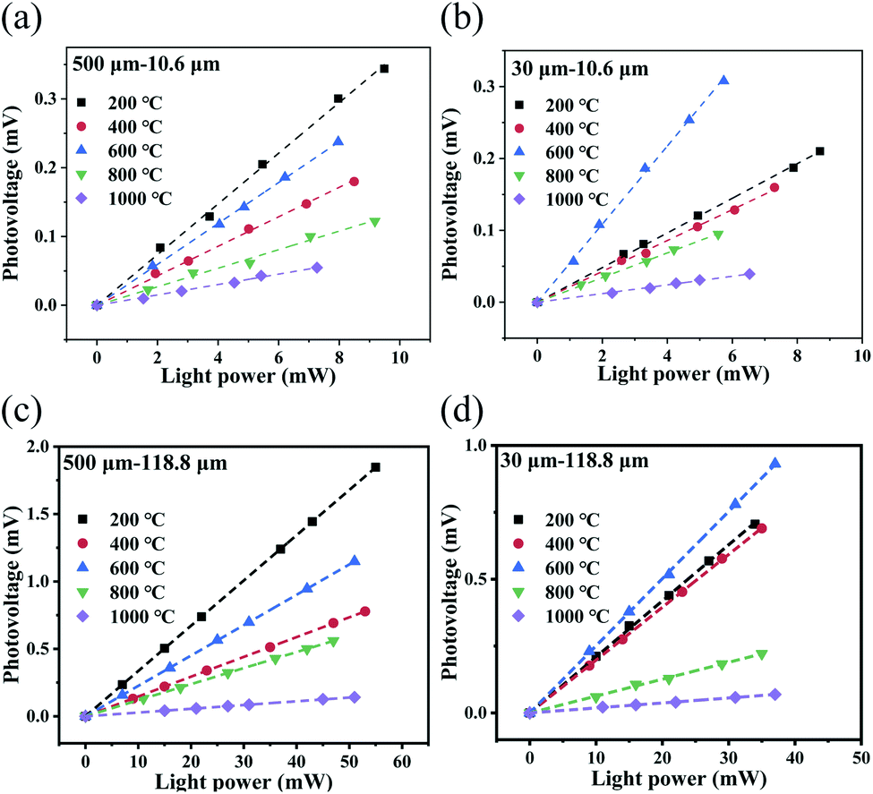
At the same time, the photovoltage generated by the detector also increases linearly with increasing MIR and terahertz power (see Fig. 8a–d), thus indicating that the detector can be used for quantitative measurement of the MIR and terahertz power.
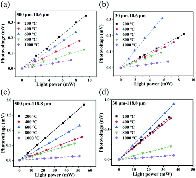 |
| | Fig. 8 Dependence of the photovoltage of the (a) 500 μm wide channel and (b) 30 μm wide channel photodetectors on the light power under 10.6 μm illumination. Dependence of the photovoltage of the (c) 500 μm wide channel and (d) 30 μm wide channel photodetectors on the light power under 2.52 THz illumination. | |
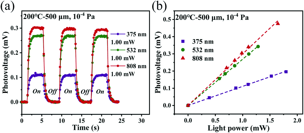
Because the main detector mechanism is the PTE effect, the heat exchange that occurs between the device and the air should have an effect on the photoresponse of the device. Therefore, transfer of the device from the atmospheric environment (105 Pa) to a vacuum cavity (10−4 Pa) for photoelectric detection was proposed. The photodetector with the 500 μm channel that was annealed at 200 °C was taken as an example, and its photoresponse characteristics under a vacuum are shown in Fig. 9a and b. When compared with the photoresponse of the same detector in the atmospheric environment (see Fig. 5a and 7a), the device shows a very obvious performance improvement under the vacuum conditions. In the atmospheric environment, the heat generated by the rGO film after light absorption has two ways to dissipate, i.e., heat exchange with the air molecules and heat conduction along the film toward the electrodes. However, the heat exchange between the rGO film and the air molecules no longer occurs under the vacuum and more heat is localized on the rGO film.63 According to eqn (1), the photovoltage generated by the detector will increase. However, this also makes the time required to reach thermal equilibrium in vacuum longer, that is, the corresponding response time under vacuum conditions is longer than that under atmospheric conditions (see Fig. S7†).
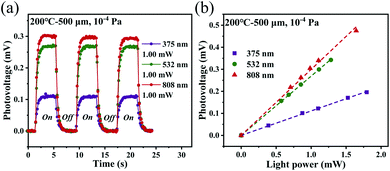 |
| | Fig. 9 (a) On–off curves of the photovoltage of a photodetector with a 500 μm wide channel annealed at 200 °C, as measured in a vacuum (10−4 Pa) under light illumination at different wavelengths. (b) Dependence of photovoltage of the photodetector with the 500 μm wide channel annealed at 200 °C on the light power in a vacuum (10−4 Pa) under light illumination at different wavelengths. | |
2.3 Important parameters of the Pd-rGO-Ti photodetector
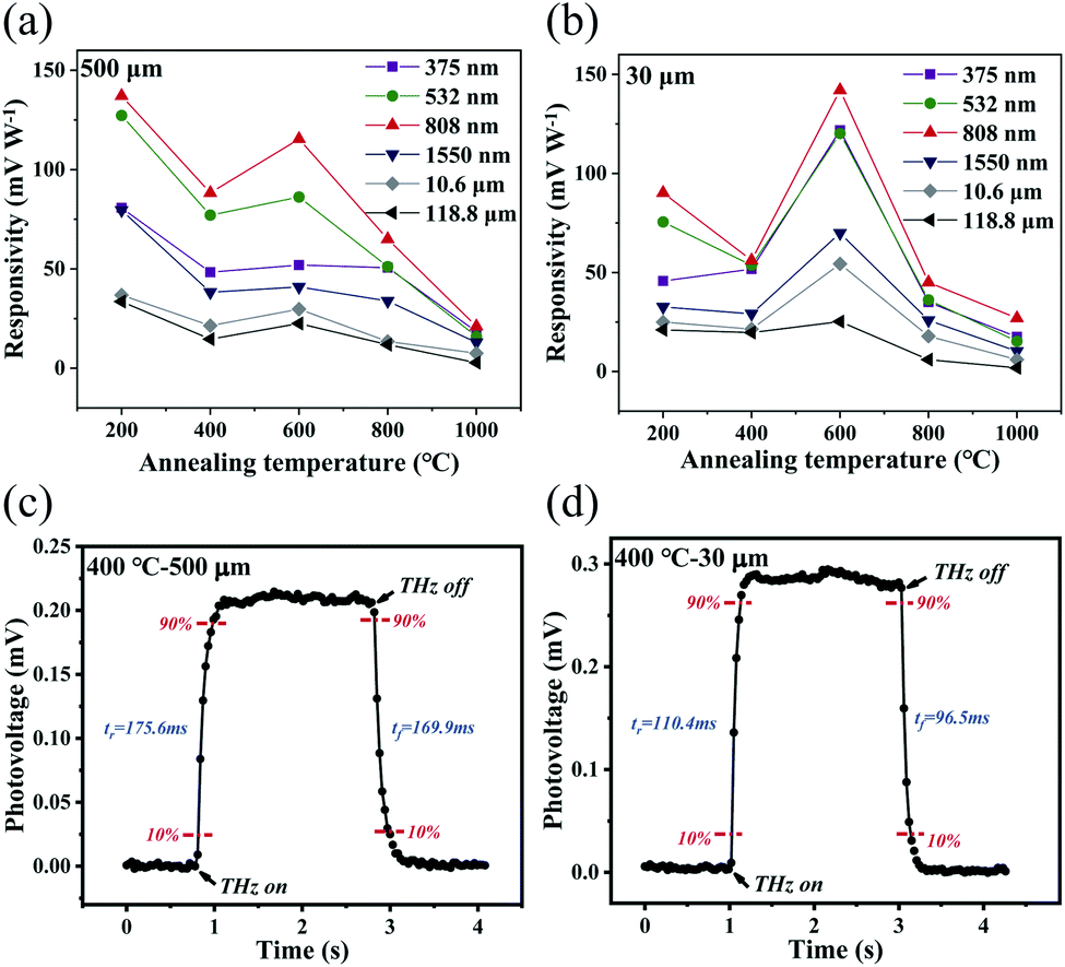
Fig. 10a and b present the dependence of the responsivity RV values of the different photodetectors on their annealing temperatures. The responsivity RV is defined as:where ΔV is the photovoltage generated at the illumination power P. The responsivity is the quantity of the unit laser power that is converted into an electrical signal, which represents the ability of the detector to convert optical signals into electrical signals and is thus an important indicator of the photodetector performance. The figures show that for the 500 μm channel detectors, the maximum responsivity appears in the detector that was annealed at 200 °C and its RV is 137.11 mV W−1. When the annealing temperature is increased, the responsivity of these detectors decreases. For the case of the 30 μm channel detectors, the responsivity initially increases and then decreases with increasing annealing temperature. The maximum responsivity appears in the detector that was annealed at 600 °C and its RV is 142.08 mV W−1. This demonstrates that the channel width has a definite influence on the responsivity of the detector. In addition, the detectors with the different annealing temperatures all show their best photoresponses under illumination at 808 nm. The phenomenon that the responsivity varies with the annealing temperature of the rGO films can be explained as follows: If electron-extracting functional groups such as the carboxyl, carbonyl, sp3-bonded hydroxyl, ether and epoxide groups in rGO are dominant, the material will be p-type, but if electron-donating functional groups such as the sp2-bonded hydroxyl, ether and epoxide groups are dominant, the material will then be n-type.34 The C 1s XPS spectra of rGO films annealed at different temperatures in Fig. 2b–f show that CO and OC–O functional groups (mainly forming carboxyl and carbonyl groups) are almost removed as the annealing temperature increases, and C–O functional groups (mainly forming hydroxyl, ether and epoxy groups) decrease slowly, while the C–C functional groups keep increasing. Therefore, the rGO films undergo p-type and n-type semiconductors transformation by increasing the annealing temperature. At the same time, the energy band structure of rGO films are changed. A portion of the carbon atoms in rGO films are bonded with oxygen-containing functional groups, including hydroxyl, epoxy, carbonyl and carboxyl groups; these carbon atoms are thus transformed from the sp2 hybridization to the sp3 hybridization and the sp3 hybridization produces a δ bond, which increases the bandgap of the rGO films. The relative ratio of the sp3 hybridization and the sp2 hybridization ultimately determines the band structure.64–67 It can be seen from Fig. 2a that the ratio of carbon content to oxygen content C/O continues to increase as the annealing temperature increases, which means that the oxygen-containing functional groups are gradually removed. Therefore, GO films first transform from insulators to semiconductors, and then from p-type semiconductors to n-type semiconductor, and then the degree of n-doping gradually decreases. When the annealing temperature is high to a certain value, rGO films are no longer n-type semiconductors, but semimetals instead. In consequence, the Seebeck coefficient SN and SP of the Pd-rGO-Ti photodetectors are greatly different, which is the main reason for the difference in responsivity of the photodetectors with different annealing temperatures. The rGO films annealed at 200 °C and 400 °C are mainly semiconductors, so the scanning photovoltages of the Pd-rGO-Ti photodetectors change from negative to positive (Fig. 4a and b and S4a, b†). While the semiconductor characteristics of the rGO films annealed at 600 °C, 800 °C and 1000 °C gradually disappear and converted to semimetals, so the Pd-rGO-Ti photodetectors continue to output positive photovoltages (Fig. 4c–e and S4c–e†).
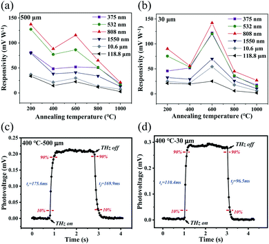 |
| | Fig. 10 Effect of annealing temperature on the responsivity of (a) the 500 μm channel detector and (b) the 30 μm channel detector under various light irradiation conditions. Rise time tr and fall time tf characteristics of the detectors annealed at 400 °C under 2.52 THz illumination with (c) the 500 μm channel and (d) the 30 μm channel. | |
Another indicator that can be used to evaluate photodetectors is the response time. When a photodetector receives laser radiation, the photovoltage will not reach a maximum immediately and the photovoltage will not be reduced immediately to zero when this radiation is removed. All photodetectors require a relaxation process and the response time is a physical quantity that reflects the response speed of the photodetectors and can be divided into the rise time tr and the fall time tf. According to the general definition, the rise time tr refers to the time taken by the photodetector to rise from 10% of the maximum photovoltage to 90% of the maximum photovoltage, while the fall time tf refers to the time taken by the detector to fall from 90% of the maximum photovoltage to 10% of the maximum photovoltage. The response times of our detectors were measured by switching the incident light on and off regularly and monitoring the resulting dynamic photovoltage changes. The time interval between two collected data points was set at 20 ms. The photoresponses of the detectors that were annealed at 400 °C under 2.52 THz irradiation are taken as an example and the rise time tr and fall time tf characteristics of the detector with the 500 μm wide channel and those of the detector with the 30 μm wide channel are shown in Fig. 10c and d, respectively. Table S1† presents a comparison of the tr and tf values of the Pd-rGO-Ti photodetectors with the different channel widths and annealing temperatures under 2.52 THz illumination. It can be seen from Table S1† that both tr and tf are in the 100–200 ms range. At the same annealing temperature, the response time of the detector with the 30 μm channel is obviously lower than that of the detector with the 500 μm channel. Therefore, channel size reduction is beneficial in improving the response speed of the detector.
The noise equivalent power (NEP) and the specific detectivity (D*) are two other important parameters used to evaluate the photodetector performance. The NEP is defined as the incident light power when the effective value of the signal voltage output by a photodetector is equal to the root-mean-square voltage value of the noise and it is actually the minimum laser power that the photodetector can detect. The NEP thus reflects the ability of the detector to detect weak laser signals, which also indicates the sensitivity of the detector. A smaller value of the NEP indicates higher detector sensitivity. The NEP is calculated as:
where
Vnoise represents the noise voltage of the detector.
3,63,68 Because our detectors do not require an external bias,
Vnoise is mainly thermal noise. Thermal noise is also known as Johnson noise and comes from the irregular thermal motion of the carriers. When the temperature is above absolute zero, each electron in a conductor or semiconductor moves randomly. Although the average value of this motion is zero, the instantaneous current perturbations generate a root-mean-square voltage value and this voltage is defined as:
| |
 | (5) |
where
k is the Boltzmann constant,
T is the thermodynamic temperature of the detector and
R is the channel resistance of the detector. The specific detectivity
D* is calculated as:
| |
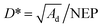 | (6) |
where
Ad is the active area of the detector.
3,63 Table 1 and S2
† show the NEP and
D* values, respectively, of the Pd-rGO-Ti photodetectors at the different annealing temperatures. It can be seen from these results that the properties of these detectors are nearly of the same order of magnitude, regardless of the annealing temperature used for the rGO films, under UV to THz illumination.
Table 1 NEP values of Pd-rGO-Ti photodetectors annealed at various temperatures under illumination in the UV to THz range
| Annealing temperature (°C) |
200 |
400 |
600 |
800 |
1000 |
| NEP(10−6 W Hz−1/2) |
375 nm |
Pd-rGO-Ti (500 μm) |
0.08 |
0.05 |
0.04 |
0.02 |
0.05 |
| Pd-rGO-Ti (30 μm) |
0.12 |
0.05 |
0.02 |
0.03 |
0.05 |
| 532 nm |
Pd-rGO-Ti (500 μm) |
0.05 |
0.03 |
0.02 |
0.02 |
0.05 |
| Pd-rGO-Ti (30 μm) |
0.07 |
0.04 |
0.02 |
0.03 |
0.06 |
| 808 nm |
Pd-rGO-Ti (500 μm) |
0.05 |
0.03 |
0.02 |
0.02 |
0.04 |
| Pd-rGO-Ti (30 μm) |
0.06 |
0.04 |
0.02 |
0.02 |
0.03 |
| 1550 nm |
Pd-rGO-Ti (500 μm) |
0.08 |
0.07 |
0.05 |
0.03 |
0.06 |
| Pd-rGO-Ti (30 μm) |
0.17 |
0.08 |
0.03 |
0.04 |
0.09 |
| 10.6 μm |
Pd-rGO-Ti (500 μm) |
0.17 |
0.12 |
0.06 |
0.09 |
0.11 |
| Pd-rGO-Ti (30 μm) |
0.21 |
0.10 |
0.07 |
0.12 |
0.27 |
| 118.8 μm |
Pd-rGO-Ti (500 μm) |
0.19 |
0.18 |
0.08 |
0.1 |
0.3 |
| Pd-rGO-Ti (30 μm) |
0.26 |
0.12 |
0.09 |
0.16 |
0.49 |
All the important parameters (i.e., the responsivity, response time, NEP and D*) of the Pd-rGO-Ti photodetectors are summarized and are compared with the parameters of other representative reported ultra-wideband photodetectors, as shown in Table 2. These results show that our suspended Pd-rGO-Ti photodetector shows an ultra-wideband response, high detectivity and good performance, thus demonstrating its promise for high-efficiency photodetection.
Table 2 Comparison of the Pd-rGO-Ti photodetectors and other representative reported ultra-wideband photodetectors
| Material |
Wavelength |
Responsivity |
Response time |
NEP (W Hz−1/2) |
D* (cm Hz1/2 W−1) |
Bias |
Ref. |
| rGO |
UV-THz |
1.82–142.08 mV W−1 |
100–200 ms |
0.02–0.49 × 10⁻⁶ |
1.06–15.80 × 10⁶ |
0 |
This work |
| rGO |
UV-THz |
0.7–87.3 mV W−1 |
13.5–49.7 ms (exponential fitting) |
0.02–2.99 × 10⁻⁶ |
0.07–6.67 × 10⁶ |
0 |
69 |
| rGO-Si |
VIS-THz |
0.62–9.0 mA W−1 |
10 s |
Non |
Non |
1 V |
70 |
| rGO |
UV-THz |
0.3–1.3 mA W−1 |
110–170 ms |
Non |
Non |
1 V |
71 |
| rGO |
UV-NIR |
0–51.46 mA W−1 |
40–161 ms |
Non |
Non |
0.5 V |
72 |
| Graphene-InSb |
VIS-MIR |
70 mA W−1 |
4 ms |
Non |
Non |
0–2 V |
73 |
| Graphene-MoS2 |
VIS-NIR |
62 A W−1 |
1.5 s |
Non |
Non |
1V |
74 |
| CNT |
VIS-MIR |
≤28 mV W−1 |
32 μs |
1.1 × 10⁻¹¹ |
4.69 × 10³ |
0 |
75 |
| CNT |
UV-THz |
3.0–17.0 mA W−1 |
0.15 ms |
Non |
6.30–35.20 × 10⁶ |
0.2 V |
76 |
| MoS2 |
UV-NIR |
28.9–50.7 mA W−1 |
Non |
Non |
0.88–1.55 × 10⁹ |
10 V |
77 |
3 Methods
3.1 Device fabrication
The rGO film was fixed on a 5 mm-wide hollow insulating substrate to prepare a suspended rGO film detector. Then a 20 nm-thick titanium film and a 20 nm-thick palladium film were deposited on the left and right ends of the rGO film, respectively, at different annealing temperatures by electron beam evaporation to form an asymmetric metal electrode structure. Periodic illumination was applied from the rear of the sample to prevent the metal film on the rGO film surface from reflecting or absorbing large quantities of light when the front of the sample was irradiated. The copper wires were connected to the electrodes through a conductive adhesive and were then connected to the external circuit for optoelectronic testing. No bias was applied to the photodetector during the experiments.
3.2 Material characterization and photoelectric measurements
All measurements were performed in air at room temperature. The Raman measurements were performed on a WITec Alpha300R confocal Raman microscopy system using a 532 nm excitation laser with a spot size diameter of approximately 500 nm. The morphologies of the rGO films with their various annealing temperatures were characterized using field emission scanning electron microscopy (FE-SEM; Merlin Compact, Carl Zeiss). The X-ray photoelectron spectra (XPS) of the rGO films were collected using an ESCALAB 250Xi X-ray photoelectron spectrometer. The illumination of the detectors was switched on and off using an electronic timer and shutter. A Keithley 2410 SourceMeter unit and a Keithley 2602B SourceMeter unit were used to measure the forward and reverse (I–V) characteristics and the time-resolved photoresponse (V–t) characteristics of the suspended nanostructure. The photoelectric test system contains four semiconductor lasers with wavelengths of 375 nm (MDL-III-375-100 mW, CNI International Trade Dept. USA), 532 nm (MGL-III-532-300 mW, CNI International Trade Dept. USA), 808 nm (MDL-III-808-100 mW, CNI International Trade Dept. USA) and 1550 nm (TEM-F-1550-30 mW, CNI International Trade Dept. USA), a 10.6 μm CO2 laser (LS3, Access Laser. USA) and a 2.52 THz (118.8 μm) gas laser (FIRL 100, Edinburgh Instruments Ltd. UK). The light spots of the 532, 808 and 1550 nm lasers and those of the 10.6 μm and 118.8 μm lasers are circles with diameters of ∼1.9, ∼4.4, 3, 3 and 3 mm, respectively. The light spot of the 375 nm laser is rectangular, with dimensions of 3.7 mm × 3.5 mm. The light power received by the samples was measured using a light power meter (PD300-1W, STARLAB). The light powers reported in the article were obtained by subtracting the optical power transmitted through the device from the optical power that was irradiated on the device surface.
4 Conclusions
We prepared suspended Pd-rGO-Ti PTE photodetectors by evaporating palladium and titanium films on the surfaces of suspended rGO films that were annealed at various temperatures and then tested the photoresponses to laser illumination over the range from UV to THz. We determined the best device structure and experimental conditions by studying the effects of different test conditions, including the location of the laser spot, the annealing temperature, the channel width between the palladium-plated area and the titanium-plated area, the laser wavelength and the atmospheric pressure, on the performance of our photodetectors. For the 500 μm channel detectors, the maximum responsivity appears in the detector that was annealed at 200 °C and its Rv is 137.11 mV W−1, while the maximum responsivity for the 30 μm channel detectors appears in the detector that was annealed at 600 °C and its Rv is 142.08 mV W−1. In addition, we explored the response time, NEP and D* characteristics of our detectors and compared them with those of other reported broadband detectors. These results show that our detectors have characteristics that include good responsivity, fast response speeds, high sensitivity and ultra-wide response bands. Our proposed fabrication method is simple, low in cost and has the potential for use in large-scale production, thus demonstrating promise for production of ultra-wideband optoelectronic devices based on rGO, and it is therefore worthy of further investment in future research.
Conflicts of interest
There are no conflicts to declare.
Acknowledgements
This work was partially supported by the NSAF (no. U1730246), the Beijing Municipal Natural Science Foundation (no. 4192024) and the National Engineering Laboratory for Dangerous Articles and Explosives Detection Technologies.
References
- Y. Z. Jin, J. P. Wang, B. Q. Sun, J. C. Blakesley and N. C. Greenham, Nano Lett., 2008, 8, 1649–1653 CrossRef CAS PubMed.
- E. Monroy, F. Omnes and F. Calle, Semicond. Sci. Technol., 2003, 18, R33–R51 CrossRef CAS.
- X. W. He, F. Leonard and J. Kono, Adv. Opt. Mater., 2015, 3, 989–1011 CrossRef CAS.
- X. Tang, M. L. Chen, A. Kamath, M. M. Ackerman and P. Guyot-Sionnest, ACS Photonics, 2020, 7, 1117–1121 CrossRef CAS.
- H. Yoo, W. G. Kim, B. H. Kang, H. T. Kim, J. W. Park, D. H. Choi, T. S. Kim, J. H. Lim and H. J. Kim, ACS Appl. Mater. Interfaces, 2020, 12, 10673–10680 CrossRef PubMed.
- M. E. Itkis, F. Borondics, A. P. Yu and R. C. Haddon, Science, 2006, 312, 413–416 CrossRef CAS PubMed.
- Y. Liu, N. Wei, Q. S. Zeng, J. Han, H. X. Huang, D. L. Zhong, F. L. Wang, L. Ding, J. Y. Xia, H. T. Xu, Z. Ma, S. Qiu, Q. W. Li, X. L. Liang, Z. Y. Zhang, S. Wang and L. M. Peng, Adv. Opt. Mater., 2016, 4, 238–245 CrossRef CAS.
- J. B. Jackson, M. Mourou, J. F. Whitaker, I. N. Duling, S. L. Williamson, M. Menu and G. A. Mourou, Opt. Commun., 2008, 281, 527–532 CrossRef CAS.
- F. Sizov, Opto-Electron. Rev., 2010, 18, 10–36 CAS.
- M. Tonouchi, Nat. Photonics, 2007, 1, 97–105 CrossRef CAS.
- L. Chen and M. Lipson, Opt. Express, 2009, 17, 7901–7906 CrossRef CAS PubMed.
- M. Piels, J. F. Bauters, M. L. Davenport, M. J. R. Heck and J. E. Bowers, J. Lightwave Technol., 2014, 32, 817–823 CAS.
- J. Kim, S. S. Joo, K. W. Lee, J. H. Kim, D. H. Shin, S. Kim and S.-H. Choi, ACS Appl. Mater. Interfaces, 2014, 6, 20880–20886 CrossRef CAS PubMed.
- Z. Su, E. S. Hosseini, E. Timurdogan, J. Sun, M. Moresco, G. Leake, T. N. Adam, D. D. Coolbaugh and M. R. Watts, Opt. Lett., 2017, 42, 2878–2881 CrossRef CAS PubMed.
- M. Zhang, L. Wang, L. Meng, X.-G. Wu, Q. Tan, Y. Chen, W. Liang, F. Jiang, Y. Cai and H. Zhong, Adv. Opt. Mater., 2018, 6, 1800077 CrossRef.
- M. Iwami, Nucl. Instrum. Methods Phys. Res., Sect. A, 2001, 466, 406–411 CrossRef CAS.
- H. W. Brandhorst and A. E. Potter, J. Appl. Phys., 1964, 35, 1997–2003 CrossRef.
- J. Wu, G. K. W. Koon, D. Xiang, C. Han, C. T. Toh, E. S. Kulkarni, I. Verzhbitskiy, A. Carvalho, A. S. Rodin, S. P. Koenig, G. Eda, W. Chen, A. H. Castro Neto and B. Oezyilmaz, ACS Nano, 2015, 9, 8070–8077 CrossRef CAS PubMed.
- Q. Guo, A. Pospischil, M. Bhuiyan, H. Jiang, H. Tian, D. Farmer, B. Deng, C. Li, S.-J. Han, H. Wang, Q. Xia, T.-P. Ma, T. Mueller and F. Xia, Nano Lett., 2016, 16, 4648–4655 CrossRef CAS PubMed.
- C. Lin, R. Grassi, T. Low and A. S. Helmyt, Nano Lett., 2016, 16, 1683–1689 CrossRef CAS PubMed.
- W. Choi, M. Y. Cho, A. Konar, J. H. Lee, G.-B. Cha, S. C. Hong, S. Kim, J. Kim, D. Jena, J. Joo and S. Kim, Adv. Mater., 2012, 24, 5832–5836 CrossRef CAS PubMed.
- Z. Zheng, T. Zhang, J. Yao, Y. Zhang, J. Xu and G. Yang, Nanotechnology, 2016, 27, 225501 CrossRef PubMed.
- L. Zeng, L. Tao, C. Tang, B. Zhou, H. Long, Y. Chai, S. P. Lau and Y. H. Tsang, Sci. Rep., 2016, 6, 20343 CrossRef CAS PubMed.
- A. Kojima, K. Teshima, Y. Shirai and T. Miyasaka, J. Am. Chem. Soc., 2009, 131, 6050–6051 CrossRef CAS PubMed.
- J. Ding, Y. Liu, H. Fang, Y. Wang, Q. Li, J.-L. Sun and Q. Yan, ACS Photonics, 2018, 5, 3172–3178 CrossRef CAS.
- F. Xia, T. Mueller, Y.-m. Lin, A. Valdes-Garcia and P. Avouris, Nat. Nanotechnol., 2009, 4, 839–843 CrossRef CAS PubMed.
- T. Mueller, F. Xia and P. Avouris, Nat. Photonics, 2010, 4, 297–301 CrossRef CAS.
- G. Konstantatos, M. Badioli, L. Gaudreau, J. Osmond, M. Bernechea, F. P. Garcia de Arquer, F. Gatti and F. H. L. Koppens, Nat. Nanotechnol., 2012, 7, 363–368 CrossRef CAS PubMed.
- Z. Sun, Z. Liu, J. Li, G.-a. Tai, S.-P. Lau and F. Yan, Adv. Mater., 2012, 24, 5878–5883 CrossRef CAS PubMed.
- I. Nikitskiy, S. Goossens, D. Kufer, T. Lasanta, G. Navickaite, F. H. L. Koppens and G. Konstantatos, Nat. Commun., 2016, 7, 11954 CrossRef CAS PubMed.
- F. Bonaccorso, Z. Sun, T. Hasan and A. C. Ferrari, Nat. Photonics, 2010, 4, 611–622 CrossRef CAS.
- K. F. Mak, M. Y. Sfeir, Y. Wu, C. H. Lui, J. A. Misewich and T. F. Heinz, Phys. Rev. Lett., 2008, 101, 196405 CrossRef PubMed.
- R. R. Nair, P. Blake, A. N. Grigorenko, K. S. Novoselov, T. J. Booth, T. Stauber, N. M. R. Peres and A. K. Geim, Science, 2008, 320, 1308 CrossRef CAS PubMed.
- N. D. K. Tu, J. Choi, C. R. Park and H. Kim, Chem. Mater., 2015, 27, 7362–7369 CrossRef.
- P. V. Kumar, M. Bernardi and J. C. Grossman, ACS Nano, 2013, 7, 1638–1645 CrossRef CAS PubMed.
- L. Liu, L. Wang, J. Gao, J. Zhao, X. Gao and Z. Chen, Carbon, 2012, 50, 1690–1698 CrossRef CAS.
- Q. Lai, S. Zhu, X. Luo, M. Zou and S. Huang, AIP Adv., 2012, 2, 032146 CrossRef.
- B. Chitara, S. B. Krupanidhi and C. N. R. Rao, Appl. Phys. Lett., 2011, 99, 113114 CrossRef.
- H. Liang, AIP Adv., 2014, 4, 107131 CrossRef.
- F. Jabbarzadeh, M. Siahsar, M. Dolatyari, G. Rostami and A. Rostami, Appl. Phys. B Laser Opt., 2015, 120, 637–643 CrossRef CAS.
- B. Chitara, L. S. Panchakarla, S. B. Krupanidhi and C. N. R. Rao, Adv. Mater., 2011, 23, 5339 CrossRef CAS.
- S. Ghosh, B. K. Sarker, A. Chunder, L. Zhai and S. I. Khondaker, Appl. Phys. Lett., 2010, 96, 163109 CrossRef.
- F. A. Chowdhury, T. Mochida, J. Otsuki and M. S. Alam, Chem. Phys. Lett., 2014, 593, 198–203 CrossRef CAS.
- H. Tian, Y. Cao, J. Sun and J. He, RSC Adv., 2017, 7, 46536–46544 RSC.
- M. Freitag, T. Low and P. Avouris, Nano Lett., 2013, 13, 1644–1648 CrossRef CAS PubMed.
- W. S. Hummers and R. E. Offeman, J. Am. Chem. Soc., 1958, 80, 1339 CrossRef CAS.
- D. Yang, A. Velamakanni, G. Bozoklu, S. Park, M. Stoller, R. D. Piner, S. Stankovich, I. Jung, D. A. Field, C. A. Ventrice and R. S. Ruoff, Carbon, 2009, 47, 145–152 CrossRef CAS.
- S. Stankovich, D. A. Dikin, R. D. Piner, K. A. Kohlhaas, A. Kleinhammes, Y. Jia, Y. Wu, S. T. Nguyen and R. S. Ruoff, Carbon, 2007, 45, 1558–1565 CrossRef CAS.
- Y. Shen, S. B. Yang, P. Zhou, Q. Q. Sun, P. F. Wang, L. Wan, J. Li, L. Y. Chen, X. B. Wang, S. J. Ding and D. W. Zhang, Carbon, 2013, 62, 157–164 CrossRef CAS.
- L. G. Cancado, A. Jorio, E. H. M. Ferreira, F. Stavale, C. A. Achete, R. B. Capaz, M. V. O. Moutinho, A. Lombardo, T. S. Kulmala and A. C. Ferrari, Nano Lett., 2011, 11, 3190–3196 CrossRef CAS PubMed.
- Y. Cao, Y. J. Zhao, Y. X. Wang, Y. Zhang, J. G. Wen, Z. R. Zhao and L. Q. Zhu, Carbon, 2019, 144, 193–201 CrossRef CAS.
- H. B. Feng, R. Cheng, X. Zhao, X. F. Duan and J. H. Li, Nat. Commun., 2013, 4, 1539 CrossRef PubMed.
- J. P. Zhao, S. F. Pei, W. C. Ren, L. B. Gao and H. M. Cheng, ACS Nano, 2010, 4, 5245–5252 CrossRef CAS PubMed.
- R. Kumar, N. Goel, R. Raliya, P. Biswas and M. Kumar, Nanotechnology, 2018, 29, 404001 CrossRef PubMed.
- J. Ito, J. Nakamura and A. Natori, J. Appl. Phys., 2008, 103, 113712 CrossRef.
- Z. Chen, J. Appenzeller, J. Knoch, Y.-m. Lin and P. Avouris, Nano Lett., 2005, 5, 1497–1502 CrossRef CAS PubMed.
- A. Javey, J. Guo, Q. Wang, M. Lundstrom and H. Dai, Nature, 2003, 424, 654–657 CrossRef CAS PubMed.
- W. Kim, A. Javey, R. Tu, J. Cao, Q. Wang and H. Dai, Appl. Phys. Lett., 2005, 87, 173101 CrossRef.
- Y. Nosho, Y. Ohno, S. Kishimoto and T. Mizutani, Appl. Phys. Lett., 2005, 86, 073105 CrossRef.
- G. Giovannetti, P. A. Khomyakov, G. Brocks, V. M. Karpan, J. van den Brink and P. J. Kelly, Phys. Rev. Lett., 2008, 101, 026803 CrossRef CAS PubMed.
- C. Zhou, J. Kong, E. Yenilmez and H. Dai, Science, 2000, 290, 1552–1555 CrossRef CAS PubMed.
- F. H. L. Koppens, T. Mueller, P. Avouris, A. C. Ferrari, M. S. Vitiello and M. Polini, Nat. Nanotechnol., 2014, 9, 780–793 CrossRef CAS PubMed.
- M. Chen, Y. X. Wang, J. G. Wen, H. H. Chen, W. L. Ma, F. Fan, Y. Huang and Z. R. Zhao, ACS Appl. Mater. Interfaces, 2019, 11, 6411–6420 CrossRef CAS PubMed.
- G. Eda, C. Mattevi, H. Yamaguchi, H. Kim and M. Chhowalla, J. Phys. Chem. C, 2009, 113, 15768–15771 CrossRef CAS.
- I. Jung, D. A. Dikin, R. D. Piner and R. S. Ruoff, Nano Lett., 2008, 8, 4283–4287 CrossRef CAS PubMed.
- K. Hu and V. V. Tsukruk, Chem. Mater., 2015, 27, 6717–6729 CrossRef CAS.
- C. Mattevi, G. Eda, S. Agnoli, S. Miller, K. A. Mkhoyan, O. Celik, D. Mastrogiovanni, G. Granozzi, E. Garfunkel and M. Chhowalla, Adv. Funct. Mater., 2009, 19, 2577–2583 CrossRef CAS.
- Y. Liu, J. Yin, P. F. Wang, Q. Q. Hu, Y. X. Wang, Y. Xie, Z. R. Zhao, Z. M. Dong, J. L. Zhu, W. D. Chu, N. Yang, J. Q. Wei, W. Y. Ma and J. L. Sun, ACS Appl. Mater. Interfaces, 2018, 10, 36304–36311 CrossRef CAS PubMed.
- J. G. Wen, Y. Y. Niu, P. F. Wang, M. Chen, W. D. Wu, Y. Cao, J. L. Sun, M. Zhao, D. M. Zhuang and Y. X. Wang, Carbon, 2019, 153, 274–284 CrossRef CAS.
- Y. Cao, J. Y. Zhu, J. Xu, J. H. He, J. L. Sun, Y. X. Wang and Z. R. Zhao, Small, 2014, 10, 2345–2351 CrossRef CAS PubMed.
- H. Yang, Y. Cao, J. H. He, Y. Zhang, B. B. Jin, J. L. Sun, Y. X. Wang and Z. R. Zhao, Carbon, 2017, 115, 561–570 CrossRef CAS.
- Y. Cao, H. Yang, Y. J. Zhao, Y. Zhang, T. T. Ren, B. B. Jin, J. H. He and J. L. Sun, ACS Photonics, 2017, 4, 2797–2806 CrossRef CAS.
- J. Xu, J. Hu, R. Wang, Q. Li, W. Li, Y. Guo, F. Liu, Z. Ullah, L. Wen and L. Liu, Appl. Phys. Lett., 2017, 111, 051106 CrossRef.
- H. Xu, J. X. Wu, Q. L. Feng, N. N. Mao, C. M. Wang and J. Zhang, Small, 2014, 10, 2300–2306 CrossRef CAS PubMed.
- S. Nanot, A. W. Cummings, C. L. Pint, A. Ikeuchi, T. Akiho, K. Sueoka, R. H. Hauge, F. Leonard and J. Kono, Sci. Rep., 2013, 3, 1335 CrossRef PubMed.
- Y. Liu, J. Yin, P. F. Wang, Q. Q. Hu, Y. X. Wang, Y. Xie, Z. R. Zhao, Z. M. Dong, J. L. Zhu, W. D. Chu, N. Yang, J. Q. Wei, W. Y. Ma and J. L. Sun, ACS Appl. Mater. Interfaces, 2018, 10, 36304–36311 CrossRef CAS PubMed.
- Y. Xie, B. Zhang, S. Wang, D. Wang, A. Wang, Z. Wang, H. Yu, H. Zhang, Y. Chen, M. Zhao, B. Huang, L. Mei and J. Wang, Adv. Mater., 2017, 29, 1605972 CrossRef PubMed.
Footnotes |
| † Electronic supplementary information (ESI) available. See DOI: 10.1039/d1ra03438c |
| ‡ These authors contributed equally to this work. |
|
| This journal is © The Royal Society of Chemistry 2021 |
Click here to see how this site uses Cookies. View our privacy policy here. 
 Open Access Article
 This Open Access Article is licensed under a Creative Commons Attribution-Non Commercial 3.0 Unported Licence
 *a
*a