
 Open Access Article
 This Open Access Article is licensed under a Creative Commons Attribution-Non Commercial 3.0 Unported Licence
Flexible hybrid photodetector based on silver sulfide nanoparticles and multi-walled carbon nanotubes†
Sung Ho Kima,
Jieun Limab,
Seonjeong Leea,
Myung Hyun Kanga,
Wooseok Song a,
Jongsun Lima,
Sunsuk Leea,
Eun Kyoung Kimb,
Joung Kyu Park*a and
Sung Myung*a
a,
Jongsun Lima,
Sunsuk Leea,
Eun Kyoung Kimb,
Joung Kyu Park*a and
Sung Myung*a
aAdvanced Materials Division, Korea Research Institute of Chemical Technology, Daejeon 34114, Korea. E-mail: parkjk@krict.re.kr; msung@krict.re.kr
bDepartment of Chemical and Biomolecular Engineering, Yonsei University, Seoul 03722, Korea
First published on 6th July 2021
Abstract
Herein, we reported a wearable photodetector based on hybrid nanocomposites, such as carbon materials and biocompatible semiconductor nanocrystals (NCs), exhibiting excellent photoresponsivity and superior durability. Currently, semiconductor nanocrystal quantum dots (QDs) containing heavy metals, such as lead or cadmium (in the form of lead sulfide (PbS) and cadmium sulfide (CdS)), are known to display excellent detection properties and are thus widely employed in the fabrication of photodetectors. However, the toxic properties of these heavy metals are well known. Hence, in spite of their enormous potential, the QDs based on these heavy metals are not generally preferred in biological or biomedical applications. These limitations, though, can be overcome by the judicious choice of alternate materials such as silver sulfide (Ag2S) NCs, which are biocompatible and exhibit multiple excitons in Ag2S QDs. The other chosen component is a carbon-based material, such as the multi-walled carbon nanotube (MWCNT), which is preferred primarily due to its strong and superior mechanical durability. In this study, a hybrid nanocomposite film was synthesized from Ag2S NCs and MWCNTs by a simple one-step fabrication process using ultrasonic irradiation. Additionally, this method did not involve any chemical functionalization or post-processing step. The size of Ag2S NCs in the hybrid film was controlled by the irradiation time and the power of the ultrasonic radiation. Further, appropriate composition ratio of the hybrid composite was optimized to balance the photo-response and mechanical durability of the photodetector. Thus, using this synthetic method, an excellent photoresponsivity property of the device was demonstrated for a near-infrared (NIR) light source with various light wavelengths. Furthermore, no visible change in photoresponsivity was observed for bending motions up to 105 cycles and for a range of angles (0–60°). This novel method provides an eco-friendly alternative to existing functional composites containing toxic heavy metals and is a promising approach for the development of wearable optoelectronic devices.
Introduction
In recent times, owing to the development of the Internet of Things (IoT) technology, wearable optoelectronic devices such as skin-like photodetectors have attracted considerable interest and attention as they are used for monitoring vital signs, blood flow, and heartbeat.1,2 In this regard, various semiconductor materials such as nanowires, perovskites, and quantum dots (QDs) have been investigated to improve the performance of photodetectors. In addition, optoelectronic detectors that can be applied to the human body require flexible and stable mechanical properties. A number of research groups have thus studied the hybridization of carbon materials (CNs) and semiconductor nanomaterials and their feasibility as complementary materials. CNs, such as carbon nanotubes (CNTs) or graphene, have been the focus of intense investigation owing to their excellent conductivity, flexibility, and durability. For example, hybrid nanostructures based on CNs have been utilized in optical devices that require ultrahigh responsivity because of the strong light absorption of TiO2 nanoparticles, MoS2, PZT, and other related organic compounds etc.3 Since the skin, consisting of the stratum corneum, epidermis, and dermis has an optical absorbance between 240 and 633 nm, NIR radiation is preferred as it is capable of sending signals from deep inside the dermis owing to its substantial penetration depth into the skin.4 There have been many research reports on optical devices using QDs with excellent optical properties in the NIR region; these are widely applied in the fabrication of patchable devices that could be attached to the human skin.5–8 QDs such as PbS, PbSe, and CdS with narrow band gaps or composites of QDs and CNs have been utilized to overcome the difficulty of applying semiconductor materials to NIR detectors, owing to their NIR detection characteristics.9–11 However, the hybrid materials employed in various optical and photonic devices contain heavy metals, such as lead and cadmium, which have toxic properties and therefore are fatal to the human body. This aspect has proven to be a critical limitation in their application to wearable devices. To overcome this issue, biocompatible Ag2S nanoparticles (Ag2S NPs) have been extensively studied for application in optoelectronic devices such as photocells and photoconductors owing to their high biocompatibility and unique absorption ability in the UV-NIR region.12,13 Highly flexible and mechanically stretchable properties should be required for wearable optoelectronic devices. However, despite the ductile properties of Ag2S film, the thin layer based on only Ag2S NPs was fractured easily under bending conditions due to the poor interface adhesion.14 To solve this issue, we synthesized Ag2S on CNTs with excellent mechanical stability and electrical conductivity, and prepared hybrid layers consisted of Ag2S NPs and CNTs.In this work, we demonstrate efficient NIR photodetectors with hybrid nanocomposite films based on Ag2S NPs and CNTs. Nanocomposites based on CNTs and Ag2S NPs (CNT–ANs) were successfully synthesized by a simple one-step solution process using ultrasonic irradiation. The sonochemical method is an effective technique for the synthesis of nanomaterials with unique shapes and properties. Moreover, this technique has a strong enough propagation pressure to create bubble formation and to hold an incomplete collapse in the solution.15 The optimized synthesis of CNT–ANs was determined by adjusting the Ag2S proportion in CNT–ANs, and the NIR detectors based on CNT–ANs were characterized against light exposure at different wavelengths and photo power densities.
Our NIR detector based on CNT–ANs exhibits an excellent photo-response of 278.22 A W−1 under light exposure (wavelength of 800 nm) with a power density of 0.15 mW cm−2, which is considerably higher than that of photodetectors based on CNT–PbS.16 In addition, this synthetic method based on CNT–ANs allowed us to improve the physical flexibility and sensitivity of the photodetector; moreover, these materials exhibit excellent properties. These synthesis methods and optoelectronic properties suggest a facile and an efficient approach for fabricating hybrid optoelectronic devices for various applications, including flexible devices and advanced wearable sensors. Furthermore, it could prove to be a viable replacement to previous devices based on heavy metal materials.
Experimental
Synthesis of CNT–ANs based multi-walled CNTs and Ag2S NPs
Ag2S NPs and CNT–ANs were prepared using a sonochemical method. For the synthesis of Ag2S NPs, 1 mmol of AgNO3 was added to 10 mL of 1-dodecanethiol (DDT). The solution was treated by ultrasound radiation for 30 min, and the resulting suspension was centrifuged several times using ethyl acetate to remove any residual by-products. The obtained Ag2S NPs were dispersed in isopropyl alcohol (1 mg mL−1). The CNT–ANs too were synthesized in a similar way, wherein, AgNO3 and multi-walled CNTs were added to the DDT solution. During the synthetic procedure, the concentrations of CNTs and DDT were kept constant while the concentration of AgNO3 was varied from 0.1 to 2 mM.Fabrication of photodetector based on CNT–ANs
A schematic of the CNT–AN-based photodetector fabrication process is shown in Fig. 1(a). Fig. 1(a–i) reveal the synthesis of CNT–ANs by the sonochemistry method using the mixture of CNT, AgNO3, and DDT. In this work, the amounts of CNT and DDT were kept constant, while the concentration of AgNO3 was adjusted to various proportions (1![[thin space (1/6-em)]](https://www.rsc.org/images/entities/char_2009.gif) :1, 1:5, 1:10, and 1:20) of CNT–ANs. As a result, CNT–ANs were successfully synthesized and dispersed in a highly volatile alcohol-based isopropyl alcohol solvent. Additionally, Ag2S NPs, when dispersed in various organic solvents, were observed to remain intact without precipitation even after three months (Fig. S1 in ESI†) because of the presence of DDT as a protective coat on the surface of NPs.17 The CNT–ANs were then spray-coated on to SiO2 or polydimethylsiloxane (PDMS) substrates for the fabrication of the CNT–ANs film. Subsequently, it was annealed in a vacuum oven to remove residual solvents present within (Fig. 1 (a-ii)). In the final step, a metallic source–drain electrode was formed by thermal evaporation on top of the CNT–ANs film, as shown in Fig. 1 (a-iii).
:1, 1:5, 1:10, and 1:20) of CNT–ANs. As a result, CNT–ANs were successfully synthesized and dispersed in a highly volatile alcohol-based isopropyl alcohol solvent. Additionally, Ag2S NPs, when dispersed in various organic solvents, were observed to remain intact without precipitation even after three months (Fig. S1 in ESI†) because of the presence of DDT as a protective coat on the surface of NPs.17 The CNT–ANs were then spray-coated on to SiO2 or polydimethylsiloxane (PDMS) substrates for the fabrication of the CNT–ANs film. Subsequently, it was annealed in a vacuum oven to remove residual solvents present within (Fig. 1 (a-ii)). In the final step, a metallic source–drain electrode was formed by thermal evaporation on top of the CNT–ANs film, as shown in Fig. 1 (a-iii).
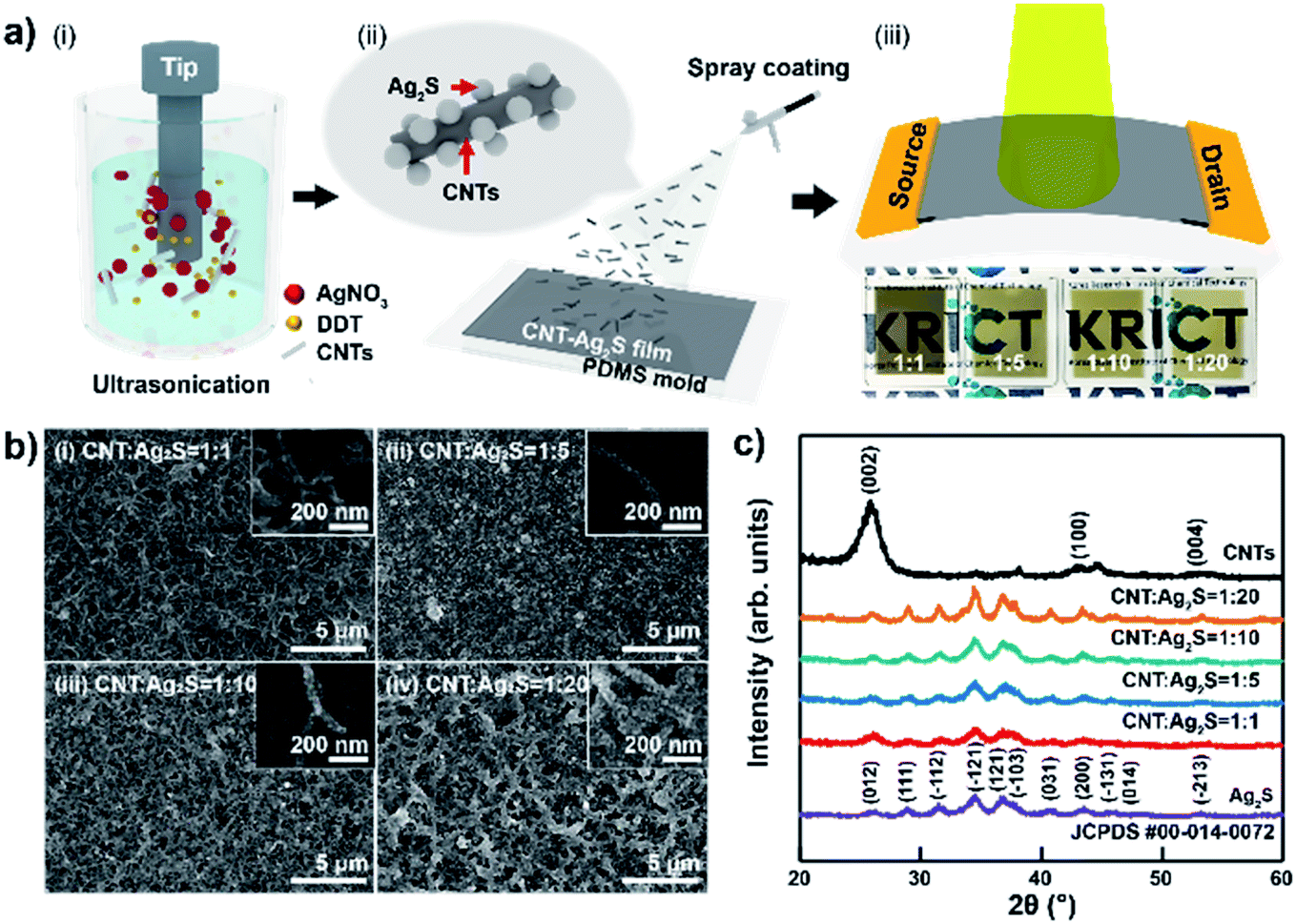 | ||
| Fig. 1 (a) Schematic of the fabrication of photodetectors based on CNT–ANs: (i) synthesis of the CNT–ANs based on multi-walled CNTs, AgNO3, and DDT by ultrasonic irradiation, (ii) hybrid structure of CNT–ANs and deposition of the CNT–ANs film on PDMS substrate by spray-coating method, (iii) fabrication of the electrodes on the CNT–ANs film for photodetector. (b) (i–iv) SEM images of CNT–ANs synthesized in various proportions. Here, the scale bar is 5 μm, and the inset shows the magnified SEM image of deposited CNT–ANs for various solution concentrations (scale bar is 200 nm). (c) XRD patterns of the CNT–ANs in various proportions. | ||
Results and discussion
The surface morphology of CNT–ANs was first investigated using field emission scanning electron microscopy (FE-SEM) (Fig. 1(b)), wherein the ratio of CNTs to Ag2S NPs was varied from 1:1 to 1:20. Ag2S NPs were found to have grown on the CNT surface, and the size of Ag2S NPs was observed to increase with a corresponding increase in the proportion of AgNO3 added. Thus, large Ag2S NPs were observed when using small capping ligands, such as DDT, at relatively high reaction temperatures. Also, transmission electron microscope (TEM) investigation confirmed that the particle size of Ag2S NPs is approximately 10 nm (Fig. S2 in ESI†), and scanning electron microscopy with energy dispersive X-ray spectroscopy (SEM-EDS) shows the existence of C, Ag and S elements in CNT–ANs (Fig. S3 in ESI†). In addition, it was observed that the density of excess Ag2S NPs increased on the CNT surfaces during the synthesis of NPs, resulting in high proportions of Ag2S NPs.18 However, cracks in the CNT–AN films by excess Ag2S NPs resulted in a decrease in the electrical conductivity between grains (Fig. S4 in ESI†).19 Additionally, Ag2S NPs in CNT–ANs have poor crystallinity when using a low-power sonication radiation. Hence, NPs were synthesized successfully under a sonication radiation of high power for over 120 min (Fig. S5 in ESI†).20 The structural characterization of the various synthesized CNT–ANs (Fig. 1(c)) was performed using X-ray diffraction (XRD). A number of Bragg diffraction peaks of α-phase Ag2S NPs were observed at 2θ values of 26.323°, 28.966°, 31.521°, 36.557°, 36.806°, 37.719°, 43.407°, and 45.426°, which could be successfully indexed as (012), (111), (−112), (−121), (121), (−103), (200), and (−131) diffraction planes (Ag2S, #JCPDF 00-014-0072), respectively.21,22 In the XRD pattern of CNTs, the observed peaks at 25.919, 42.959, and 53.29° were assigned to (002), (100), and (004) diffraction planes (CNTs, #JCPDF 00-058-1638), respectively. Moreover, the XRD peak intensity of CNT–ANs increased with an increase in NP precursors indicating that the crystallinity of Ag2S was improved. Further, the observed XRD pattern of CNT–ANs was quite similar to that of the Ag2S NPs, suggesting that the internal phase structure of Ag2S does not undergo any significant change when combined with CNT. In particular, no characteristic (002) diffraction peaks of CNTs were observed in the XRD pattern of the hybrid nanocomposite CNT–ANs. The primary reason for this trend is the presence of low amounts of CNTs as large amounts of Ag2S are present on the surface. Moreover, as the ratio of Ag2S increased, the full width at half maximum (FWHM) value of the (−112) peak decreased, indicating that the particle size increased gradually.23
The surface chemical composition analysis of different proportions of CNT–AN samples was investigated via X-ray photoelectron spectroscopy (XPS) (Fig. 2(a)). The Ag 3d core level spectrum for the Ag 3d5/2 and Ag 3d3/2 peaks showed a strong intensity and a set of symmetric peaks at 368.08 and 374.28 eV, respectively. There were no shoulder or satellite peaks observed between the Ag 3d peaks. Further, the intensity of the peak too was observed to increase with an increase in the concentration of Ag2S. In the S 2p core-level spectrum, the S 2p1/2 and S 2p3/2 peaks were observed at 162.58 and 161.48 eV, respectively.24 The intensity of the silver peak was observed to increase gradually with the respective atomic ratios ranging between 1:1.33 and 1:2 (Fig. S6 in ESI†). All the obtained XPS profiles were calibrated against the C 1s peak located at 284.48 eV. The peak at 284.7 eV was assigned to the sp2 hybridized carbon (C–C), and the peak at 285.5 eV was assigned to the C–S bonding peak according to sulfur. When the survey peak in CNT–ANs was measured with various proportions of Ag2S, the intensity of the carbon peak decreased gradually with a proportional increase in the amount of Ag2S. In addition, as the ratio of Ag2S in the CNT–ANs sample increased, the intensity of the C–S bonding peak too was observed to become stronger. To compare the characteristics of CNT–ANs, three different samples of thin films were prepared based on CNT–ANs, mixtures of DDT with CNTs, and CNTs using the same synthetic method (Fig. S7 in ESI†). When DDT was added to the CNT solution, sulfur peaks associated with the DDT solution were observed. In addition, the mixture of DDT and CNT exhibited a low intensity for C–O and COOH bonding and a high intensity for the C–S bonding. On the other hand, when AgNO3 was added to the CNT–DDT solution mixture, sulfur peaks related to Ag2S in the thin film were observed. Moreover, a higher intensity of C–S bonding in C 1s was obtained this time when compared to its intensity values in the CNT–DDT only mixture (i.e. the mixture without AgNO3). This indicates that sulfur is formed first on the CNTs and AgNO3 reacts sequentially to form Ag2S NPs. Fourier transform-infrared (FT-IR) spectroscopy was used to investigate the surface modification of CNTs by DDT and AgNO3.25 The results are shown in Fig. S8 in ESI.† For CNTs, the spectra exhibited almost no functional groups on the surface. However, after synthesis, the CNTs revealed the presence of various kinds of functional groups. The bands at 2917 and 2848 cm−1 correspond to the C–H stretching vibrations. This indicates that the Ag2S NPs are bound to CNTs by a variety of functional groups.
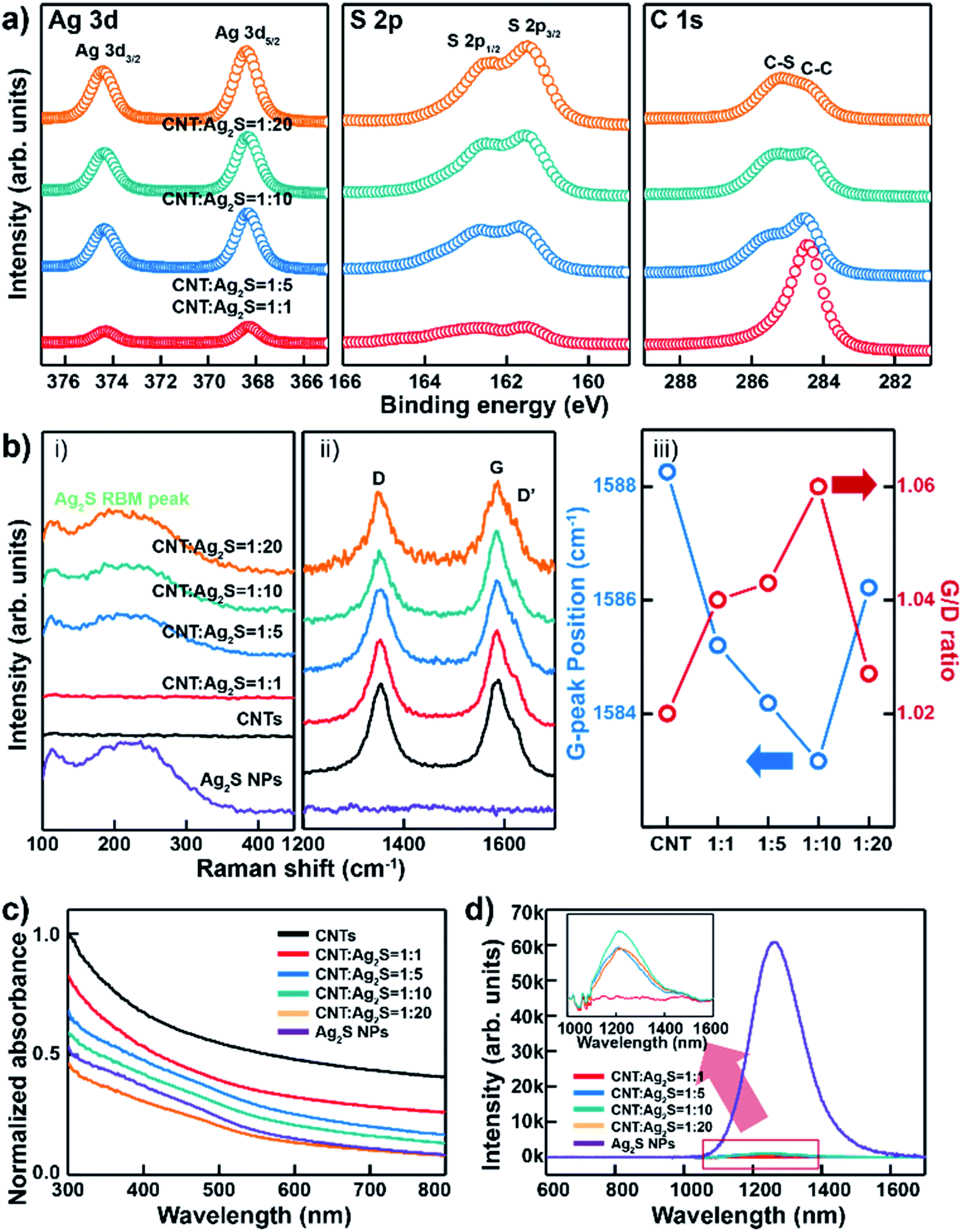 | ||
| Fig. 2 Characterization of CNT–ANs synthesized in various proportions (1:1, 1:5, 1:10, 1:20 (CNT:Ag2S)). (a) XPS profiles of the Ag 3d, S 2p, and C 1s core levels of the CNT–ANs. (b) Raman spectra of CNT–ANs under the 514 nm laser excitation. (i) RBM peaks of Ag2S, (ii) D, D′, and G peak positions, (iii) G/D ratio and G peak positions. (c) Absorption spectra of CNT–ANs (d) PL emission spectra of the CNT–ANs at an excitation wavelength of 460 nm. | ||
As shown in the Raman spectra of CNTs, Ag2S NPs, and CNT–ANs (Fig. 2(b)-(i and ii)), the D-band, G-band, and D′-band peaks were measured according to the radial breathing mode (RBM) of Ag2S.26 In this case, the Raman spectra were recorded at an excitation wavelength of 514 nm. As the peaks at 1437 cm−1 arise from the vibrations of silver metal and sulfur oxide compounds, which are formed due to the photo-induced decomposition of Ag2S in air under the exposure of high laser excitation power (Fig. S9 in ESI†), the measurement was performed at a relatively low power (power < 0.86 mW) of the laser radiation.27 The RBM peak in the Raman spectrum originated from the phonon vibration mode of Ag–S bonding in Ag2S NPs. Broad peaks at 250 cm−1 were observed for Ag2S NPs, but not for CNTs. It is worth noting that Ag2S NPs were well formed on the CNT surface. However, in the case of the 1:1 (CNT:Ag2S) proportion, the RBM peak was not obtained because Ag2S NPs were not synthesized yet, which can be seen from the XPS results presented in Fig. 2(a). It seems that the amount of Ag2S was too small for the complete synthesis of the NPs. Additionally, with an increase in the proportion of Ag2S, a blue-shift of the G-band and an increase in the intensity ratio of the D and G bands (ID/IG) were observed (Fig. 2(b-iii)). This could be attributed to the increasing density of Ag2S on the CNT surface and the net n-type doping effect of Ag2S NPs on CNTs.28 In the case of the mixture with a 1:20 (CNT:Ag2S) ratio, the defect concentration increased and a reverse shift from non-bonding Ag2S NPs was observed.
Fig. 2(c) shows the absorption spectra of CNTs, Ag2S, and CNT–ANs. No characteristic absorption peak was observed for CNTs, while a peak of absorption in the 400–500 nm range was recorded for Ag2S NPs and CNT–ANs.29 The charge transfer between Ag2S NPs and CNT–ANs was investigated by photoluminescence (PL) analysis (Fig. 2(d)). Ag2S NPs show a PL emission band at approximately 1264.89 nm, while the CNT–AN films show a relatively low peak intensity than Ag2S. PL emission quenching of Ag2S NPs in CNT–ANs resulted due to the charge transfer from photo-excited Ag2S NPs to CNTs.30 In addition, a remarkable blue-shift of the emission peak was observed at 1210.25 nm for all the films with mixture ratios of 1:5, 1:10, and 1:20 (CNT:Ag2S) except for the film with the proportion ratio of 1:1 (CNT:Ag2S), which did not exhibit any PL peak. This blue-shift is explained by the change in the initial electronic density and confinement energy of the Ag2S NPs.31,32
Thin film layers based on CNT–ANs for flexible photodetectors were fabricated by spray-coating on an ultraviolet light-treated SiO2 substrate. Here, the thickness of the CNT–ANs was about 480 nm (Fig. S10 in ESI†). Source/drain electrodes (5 nm Cr/70 nm Au) were deposited on the CNT–ANs film through a shadow mask. The channel length and width of the device were 50 and 500 μm, respectively. The current–voltage (I–V) curve shows the conductivity of each synthesized CNT–ANs film within 1 V (Fig. 3(a)). The curve shows a clear linear response wherein the current of the CNT–ANs film was observed to increase with a corresponding decrease in Ag2S proportions. Fig. 3(b) shows the photocurrent of the fabricated photodetectors based on CNT–ANs under white light exposure. The CNT–ANs device with a 1:10 (CNT:Ag2S) proportion exhibits the best on-state photocurrent with the recorded value being 26.03 μA. Photoresponsivity (R) of the 1:10 CNT–Ag2S photodetector with the best photocurrent was calculated by using R = (IPhoto − IDark)/PS, where P is light intensity, S is the illuminated area of the channel. R of our device is 8.3 A W−1 under white light exposure. In addition, the photosensitivity and detectivity were 5.7 × 10⁴ and 1.7 × 10¹⁰ Jones, respectively. The value of the gain (G) coefficient at wavelengths of 350, 550, 800 nm were 29.52, 18.78, 12.91, respectively. It is notable that as the wavelength of incident light increases, the gain of photodetectors decreases. Fig. 3(c) exhibits the typical photoresponsivity of CNT–ANs (with a 1:10 (CNT:Ag2S) proportion) as a function of the source–drain voltage under light exposure with a power density of 12.26 mW cm−2. The observed change of photocurrent with increasing source–drain voltage leads to an increase in the current of the photodetector. The trend continued until the maximum current was reached at a source–drain voltage of 1 V. Fig. S11 in ESI† show the photocurrent in logarithmic scale according to drain voltage. Fig. 3(d) shows a schematic of the energy band alignment with the photodetection mechanism. In the case of nanoscale NPs, the band gap broadening phenomenon can occur because of the strong internal forces to the lattice of the nanoscale materials. Also, Akamatsu et al. showed that the band gap of Ag2S NPs larger than 5 nm almost equal to that of the Ag2S bulk value.33 As mentioned before, the diameter of Ag2S NP in this study was 10 nm, which indicates that there is no quantum confinement effect on NPs and the band gap (Eg) of our Ag2S NP is around 1 eV.34,35 The conduction band minimum (CBM) and valence band maximum (VBM) of Ag2S NPs are taken to be 4.5 and 5.4 eV, respectively.36 The work function of CNTs is in the range of 4.7–4.95.37,38 When the device is exposed to light, photoexcited electrons are transferred from the Ag2S NPs to the CNTs owing to the efficient electron conductivity of the CNTs, which leads to a decrease in the PL intensity.30,31
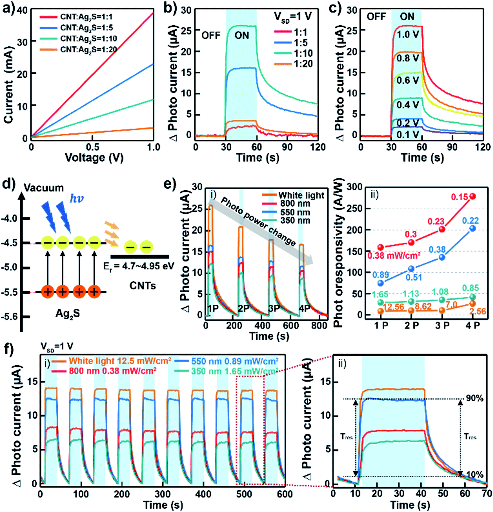 | ||
| Fig. 3 Optoelectrical properties of CNT–AN-based films on SiO2 substrates. (a) Current–voltage (I–V) characteristic curves of the CNT–AN-based films. (b) Photocurrent of photodetector based on CNT–ANs under white light exposure. (c) photocurrent of photo devices based on CNT–ANs with a 1:10 (CNT:Ag2S) proportion as a function of the source–drain bias voltage. (d) Schematic energy band diagram of the Fermi levels of CNT and Ag2S NPs. (e) Photo responsivity of the photodetector based on CNT–ANs with a 1:10 (CNT:Ag2S) proportion. (i and ii) Photocurrent due to the exposure to various light sources such as white light, and light at 800, 550, and 350 nm wavelength. The source–drain bias voltage (VSD) is 1 V. (f) (i) Photo-response of devices based on CNT–ANs with a 1:10 (CNT:Ag2S) proportion under cyclic illumination with white-light, 800, 550, and 350 nm for a corresponding power density of 12.5, 0.38, 0.89, and 1.65 mW cm−2, and (ii) the response times (τres) and decay time (τdec) under white light illumination. | ||
We obtained the power dependence of the photocurrent of photodetectors based on CNT–ANs with a 1:10 (CNT:Ag2S) at a source–drain voltage of 1 V under illumination with white light, with light having wavelengths of 800, 550, and 350 nm (Fig. 3(e)-(i and ii)), respectively. The obtained results indicated that the photocurrent changed continuously with the photo-power density, with the best recorded photo-responsivity being 278.22 A W−1 at a wavelength of 800 nm (0.15 mW cm−2) of the NIR light source. This response, displaying an excellent reactivity in the NIR wavelength range, is notably higher than that of the PbS/CNT-based photodetectors reported in previous studies.16,39 This could be ascribed to the excellent absorption characterization of Ag2S NPs in the NIR region.40,41
In this study, CNT–ANs that do not contain heavy metals such as Pb or Cd, were successfully synthesized and applied in the fabrication of flexible and implantable NIR photodetectors. Fig. 3(f)-(i) shows the photo-response of devices based on CNT–ANs with a 1:10 (CNT:Ag2S) proportion under cyclic illumination with white light and at wavelengths 800, 550, and 350 nm for corresponding power densities of 12.5, 0.38, 0.89, and 1.65 mW cm−2. The recorded photocurrents were observed to be constant for up to 600 s, further confirming the superior performance and stability of the devices. Fig. 3(f)-(ii) shows the response time (τres) and decay time (τdec) under white-light illumination. The measured τres, for which the photocurrent rises from 10 to 90% of maximum, was 1.18 s, while the measured τdec was 15.16 s. Additionally, in cases where the illumination wavelengths were below 800, 550, and 350 nm, the response speed was observed to decrease slightly (Table S1 in ESI†).
To verify the applicability of wearable devices to human skin and the durability of our CNT–AN films for flexible photodetectors, flexible devices based on CNT–ANs were fabricated on a PDMS substrate by spray-coating. The sensing performance was measured according to the bending cycles and bending angles (Fig. 4(a)). In this work, a bending tester (JUNIL TECH Co., LTD-JIBT-610-Radius Bending) was used with a bending radius of 5 mm (Fig. 4(b)). Although the photo-response was relatively reduced because of the quenching effect of the substrate, the photodetection performance remained stable even after 105 bending cycles (Fig. 4(c)). Moreover, the photocurrent maintains almost the same response at high bending angles (0–60°) (Fig. 4(d)).42 This result demonstrates the good mechanical stability of the devices owing to the superior mechanical flexibility characteristic of CNTs. This approach, thus, may pave the way forward for the fabrication of advanced flexible photoelectronic devices.
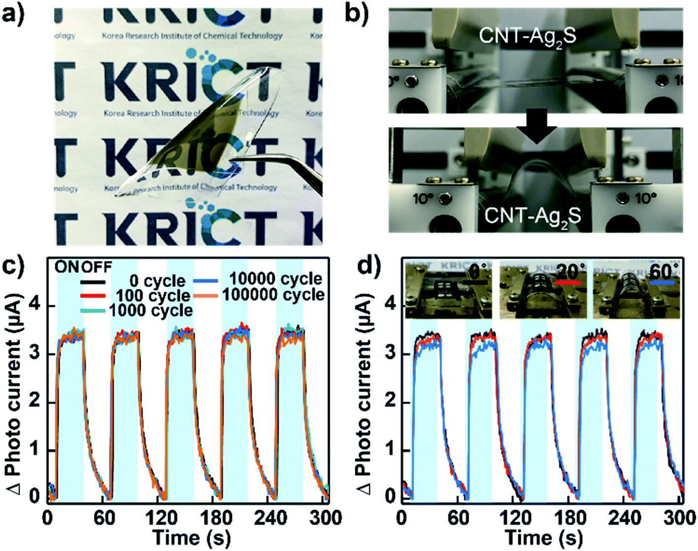 | ||
| Fig. 4 Flexibility and durability performances of films based on CNT–ANs with a 1:10 (CNT:Ag2S) proportion. (a) Photograph of CNT–ANs film on a PDMS mold substrate. (b) Bending test of CNT–ANs films. (c) Photo-response according to the number of bending cycles (bending radius = 5 mm). (d) Photo-response after bending at wide angles (0°–60°). The insets show bending test of CNT–ANs. | ||
Conclusions
In summary, lead-free hybrid structures based on CNTs and biocompatible Ag2S NPs were successfully synthesized by ultrasonication to produce high-performance flexible photodetectors. The synthesized CNT–ANs exhibited high responsivity and excellent sensitivity under various illumination wavelengths. In particular, NIR detectors based on CNT–ANs exhibited an excellent photo-response of 278.22 A W−1 under a light exposure with a power density of 0.15 mW cm−2 and 800 nm wavelength, showing the possibility of its application as an NIR detector. In addition, flexible photodetectors based on CNT–ANs were mechanically and electrically stable after 105 bending cycles and high bending angles. We believe that our synthesis methods and their optoelectronic properties present a facile and efficient approach for manufacturing wearable optoelectronic devices.Author contributions
S. K, J. L., S. L., M.K. and W. S. contributed to the fabrication of photodetectors with hybrid nanocomposite films based on Ag2S NPs and CNTs. J. L., S. L., S. S. L., and J. P. performed experimental measurements and analysed the data. S. K and S. M. conceived and designed the experiments, and S. K., S. L. and S. M. wrote the manuscript, and all authors discussed the results and commented on the manuscript.Conflicts of interest
There are no conflicts to declare.Acknowledgements
This research was supported by the Nano/Material Technology Development Program through the National Research Foundation of Korea (NRF) funded by the Ministry of Education, Science and Technology (NRF-2017M3D9A1073502). This research was also supported by the Bio & Medical Technology Development Program of the National Research Foundation (NRF) funded by the Ministry of Science, ICT & Future Planning (NRF-2020M3A9E4039224).References
- J. An, T. D. Le, C. H. J. Lim, V. T. Tran, Z. Zhan, Y. Gao, L. Zheng, G. Sun and Y. J. Kim, Adv. Sci., 2018, 5, 1800496 CrossRef PubMed.
- Y. Liu, M. Pharr and G. A. Salvatore, ACS Nano, 2017, 11, 9614–9635 CrossRef CAS PubMed.
- X. Chen, K. Shehzad, L. Gao, M. Long, H. Guo, S. Qin, X. Wang, F. Wang, Y. Shi, W. Hu, Y. Xu and X. Wang, Adv. Mater., 2020, 32, 1902039 CAS.
- M. J. van Gemert, S. L. Jacques, H. J. Sterenborg and W. M. Star, IEEE Trans. Biomed. Eng., 1989, 36, 1146–1154 CrossRef CAS PubMed.
- C. Cheng, S. Li, A. Thomas, N. A. Kotov and R. Haag, Chem. Rev., 2017, 117, 1826–1914 CrossRef CAS PubMed.
- E. O. Polat, G. Mercier, I. Nikitskiy, E. Puma, T. Galan, S. Gupta, M. Montagut, J. J. Piqueras, M. Bouwens, T. Durduran, G. Konstantatos, S. Goossens and F. Koppens, Sci. Adv., 2019, 5, 7846 CrossRef PubMed.
- W. Bai, T. Kuang, C. Chitrakar, R. Yang, S. Li, D. Zhu and L. Chang, Biosens. Bioelectron., 2018, 122, 189–204 CrossRef CAS.
- N. P. Shetti, A. Mishra, S. Basu, R. J. Mascarenhas, R. R. Kakarla and T. M. Aminabhavi, ACS Biomater. Sci. Eng., 2020, 6, 1823–1835 CrossRef CAS.
- X. Yu, S. Zhang, H. Zeng and Q. J. Wang, Nano Energy, 2016, 25, 34–41 CrossRef CAS.
- Y. Gong, P. Adhikari, Q. Liu, T. Wang, M. Gong, W. L. Chan, W. Y. Ching and J. Wu, ACS Appl. Mater. Interfaces, 2017, 9, 11016–11024 CrossRef CAS PubMed.
- Z. Sun, Z. Liu, J. Li, G. A. Tai, S. P. Lau and F. Yan, Adv. Mater., 2012, 24, 5878–5883 CrossRef CAS.
- C. Wang, Y. Wang, L. Xu, D. Zhang, M. Liu, X. Li, H. Sun, Q. Lin and B. Yang, Small, 2012, 8, 3137–3142 CrossRef CAS PubMed.
- Y. Zhang, G. Hong, Y. Zhang, G. Chen, F. Li, H. Dai and Q. Wang, ACS Nano, 2012, 6, 3695–3702 CrossRef CAS.
- Y. Lei, L. Gu, X. Yang, Y. Lin and Z. Zheng, Adv. Mater. Interfaces, 2021, 8, 2002255 CrossRef CAS.
- H. Xu, B. W. Zeiger and K. S. Suslick, Chem. Soc. Rev., 2013, 42, 2555–2567 RSC.
- I. Ka, V. Le Borgne, K. Fujisawa, T. Hayashi, Y. A. Kim, M. Endo, D. Ma and M. A. El Khakani, Mater. Today Energy, 2020, 16, 100378 CrossRef.
- J. Lee, M. Kim, C. K. Hong and S. E. Shim, Meas. Sci. Technol., 2007, 18, 3707–3712 CrossRef CAS.
- Y. Zhang, Y. Liu, C. Li, X. Chen and Q. Wang, J. Phys. Chem. C, 2014, 118, 4918–4923 CrossRef CAS.
- G. Hwang, Y.-T. Shieh and K. Hwang, Adv. Funct. Mater., 2004, 14, 487–491 CrossRef CAS.
- Y. Ding, J. Zheng, X. Xia, T. Ren and J. Kan, LWT--Food Sci. Technol., 2016, 67, 206–213 CrossRef CAS.
- S. I. Sadovnikov and E. Yu Gerasimov, Nanoscale Adv., 2019, 1, 1581–1588 RSC.
- A. I. Gusev and S. I. Sadovnikov, Thermochim. Acta, 2018, 660, 1–10 CrossRef CAS.
- H. Doh, S. Hwang and S. Kim, Chem. Mater., 2016, 28, 8123–8127 CrossRef CAS.
- W. Jiang, Z. Wu, X. Yue, S. Yuan, H. Lu and B. Liang, RSC Adv., 2015, 5, 24064–24071 RSC.
- K. Cheng, X. Yang, X. Zhang, J. Chen, J. An, Y. Song, C. Li, Y. Xuan, R. Zhang, C. Yang, X. Song, Y. Zhao and B. Liu, Adv. Funct. Mater., 2018, 28, 1803118 CrossRef.
- Y. Delgado-Beleño, M. Cortez-Valadez, C. E. Martinez-Nuñez, R. Britto Hurtado, R. A. B. Alvarez, O. Rocha-Rocha, H. Arizpe-Chávez, A. Perez-Rodríguez and M. Flores-Acosta, Chem. Phys., 2015, 463, 106–110 CrossRef.
- S. I. Sadovnikov, E. G. Vovkotrub and A. A. Rempel, Dokl. Phys. Chem., 2018, 408, 81–84 CrossRef.
- L. G. Bulusheva, A. V. Okotrub, A. G. Kurenya, H. Zhang, H. Zhang, X. Chen and H. Song, Carbon, 2011, 49, 4013–4023 CrossRef CAS.
- M. H. Kang, S. H. Kim, S. Jang, J. E. Lim, H. Chang, K. Kong, S. Myung and J. K. Park, RSC Adv., 2018, 8, 28447–28452 RSC.
- I. Ka, V. Le Borgne, D. Ma and M. A. El Khakani, Adv. Mater., 2012, 24, 6289–6294 CrossRef CAS.
- D. Wang, J. K. Baral, H. Zhao, B. A. Gonfa, V. Truong, M. A. El Khakani, R. Izquierdo and D. Ma, Adv. Funct. Mater., 2011, 21, 4010–4018 CrossRef CAS.
- W. Feng, C. Qin, Y. Shen, Y. Li, W. Luo, H. An and Y. Feng, Sci. Rep., 2015, 4, 3777 CrossRef PubMed.
- K. Akamatsu, S. Takei, M. Mizuhata, A. Kajinami, S. Deki, S. Takeoka, M. Fujii, S. Hayashi and K. Yamamoto, Thin Solid Films, 2000, 359, 55–60 CrossRef CAS.
- R. Zamiri, H. Abbastabar Ahangar and A. Zakaria, et al., Chem. Cent. J., 2015, 9, 28 CrossRef PubMed.
- R. V. Kumar, O. Palchik, Y. Koltypin, Y. Diamant and A. Gedanken, Ultrason. Sonochem., 2002, 9, 65–70 CrossRef CAS.
- Y. Lei, H. Jia, W. He, Y. Zhang, L. Mi, H. Hou, G. Zhu and Z. Zheng, J. Am. Chem. Soc., 2012, 134, 17392–17395 CrossRef CAS PubMed.
- M. Shiraishi and M. Ata, Carbon, 2001, 39, 1913–1917 CrossRef CAS.
- P. Liu, Q. Sun, F. Zhu, K. Liu, K. Jiang, L. Liu, Q. Li and S. Fan, Nano Lett., 2008, 8, 647–651 CrossRef CAS PubMed.
- L. Gao, D. Dong, J. He, K. Qiao, F. Cao, M. Li, H. Liu, Y. Cheng, J. Tang and H. Song, Appl. Phys. Lett., 2012, 24, 6289–6294 Search PubMed.
- Y. Shen, J. Lifante, E. Ximendes, H. D. A. Santos, D. Ruiz, B. H. Juárez, I. Zabala Gutiérrez, V. Torres Vera, J. Rubio Retama, E. Martín Rodríguez, D. H. Ortgies, D. Jaque, A. Benayas and B. Del Rosal, Nanoscale, 2019, 11, 19251–19264 RSC.
- A. H. Poh, F. R. M. Adikan and M. Moghavvemi, Med. Biol. Eng. Comput., 2020, 58, 1159–1175 CrossRef PubMed.
- J. F. Miethe, F. Lubkemann, N. C. Bigall and D. Dorfs, Front. Chem., 2019, 7, 1–11 CrossRef.
Footnote |
| † Electronic supplementary information (ESI) available. See DOI: 10.1039/d1ra03385a |
| This journal is © The Royal Society of Chemistry 2021 |