
 Open Access Article
 This Open Access Article is licensed under a Creative Commons Attribution-Non Commercial 3.0 Unported Licence
Study of deposition parameters and growth kinetics of ZnO deposited by aerosol assisted chemical vapor deposition†
Sergio Sánchez-Martín *ab,
S. M. Olaizolaab,
E. Castañoab,
E. Urionabarrenetxeaab,
G. G. Mandayoab and
I. Ayerdiab
*ab,
S. M. Olaizolaab,
E. Castañoab,
E. Urionabarrenetxeaab,
G. G. Mandayoab and
I. Ayerdiab
aCEIT-Basque Research and Technology Alliance (BRTA), Manuel Lardizabal 15, 20018 Donostia/San Sebastián, Spain. E-mail: iayerdi@tecnun.es
bUniversidad de Navarra, Tecnun, Manuel Lardizabal 13, 20018 Donostia/San Sebastián, Spain
First published on 21st May 2021
Abstract
Aerosol-assisted Chemical Vapor Deposition (AACVD) is a thermally activated CVD technique that uses micro-droplets as deposition precursors. An AACVD system with a custom-designed reaction chamber has been implemented to grow ZnO thin films using zinc chloride as a precursor. The present work aims to study the impact of the deposition parameters on the thin film, as well as the microstructure evolution and growth kinetics. Aerosol flow has an effect on the density of nucleation sites and on the grain size. The temperature affects the morphology of the grown ZnO, showing a preferential orientation along the c-axis for 350 °C, 375 °C and 400 °C substrate temperatures. The microstructural evolution and the growth kinetics are also presented. A different evolution behavior has been observed for 350 °C, where nucleation site density is the highest at the early stages and it decreases over time in contrast with the cases of 375 °C and 400 °C, where there is an initial increase and a subsequent decrease. The activation energy of the chemical reaction is 1.06 eV. The optical characterization of the material has been performed through reflection measurements showing a relationship between the spectrum and the ZnO film thickness. The electrical characterization has been done by means of an interdigital capacitor, with which it is possible to measure the grain and grain boundary resistance of the material. Both resistances are of the order of 105–106 Ω.
1 Introduction
ZnO is a semiconductor material with wide relevance in the scientific community due to its electronic and optical properties.1 ZnO is a n-type II–IV semiconductor with a hexagonal wurtzite structure and a direct bandgap of 3.37 eV. It has some advantages over other oxide materials such as In2O3, TiO2 or SnO2, namely, lower cost and non-toxicity. With a large exciton binding energy, ZnO is emerging as a very promising material for optoelectronic applications in the near UV range of the spectrum,2,3 e.g. Light Emitting Diodes (LEDs).4 ZnO it is also valuable as a chemoresistive material and can act as a gas sensor due to its chemical and thermo-mechanical stability.5,6 It also has applications in the field of spintronics.7The deposition technique and its parameters have a strong influence on the quality and properties of a deposited thin film. Theoretical and experimental procedures have been addressed to study the growth methods. Some theoretical works study the growth mechanisms by using simulation methods such as molecular dynamics,8,9 or the Density Functional Theory (DFT).10,11 On the other hand, there are many experimental works studying different deposition techniques. Considering that morphology and stability are crucial factors for material applications, there are several advanced deposition techniques with high control over the ZnO thin film growth. Pulsed Laser Deposition (PLD) has been used as a ZnO deposition technique by G. Wisz, et al.12 Microstructure and optical properties of ZnO films prepared by sol–gel have been analyzed by H. Li et al.,13 P. Boryło et al., have studied the influence of the temperature in an Atomic Layer Deposition (ALD) process.14 Structural studies of ZnO obtained employing DC sputtering and electron beam evaporation have been done by M. E. L. Sabino et al.15 Microstructural analysis has been performed by M. Krunks et al. of ZnO nanostructured layers grown by spray pyrolysis.16 Aerosol Assisted Chemical Vapor Deposition (AACVD) technique has also been used, depicting high stoichiometric and structural control of the grown films as C. E. Knapp et al., show in their work.17
AACVD has some characteristics that make it a competitive thin film deposition method: (i) low temperature requirements, (ii) good stoichiometric and morphology control, (iii) high deposition rate, (iv) low cost and (v) wide availability of precursors.17–19 The precursors usually employed for the AACVD deposition of ZnO are zinc chloride,20 zinc acetate21 and zinc acetylacetonate.22,23
Previous works performed with the AACVD technique using zinc chloride as a precursor are focused on the temperature influence and the use of dopants.20,24 However, there is a lack of reports about the growth kinetics and the impact of process parameters such as aerosol flow rate on the AACVD growth of ZnO thin films.
In this work, ZnO thin films are grown by AACVD technique on silicon and alumina substrates using zinc chloride as a precursor. The effect of deposition parameters, as aerosol flow or substrate temperature, are studied through scanning electron microscopy (SEM). In addition to SEM imaging, microstructural evolution and growth kinetics are also analyzed by X-ray diffraction (XRD) and profilometry. A Matlab program has been developed for determining particle size and nucleation site density. The electrical and optical properties are also studied by means of impedance spectroscopy and reflection measurements respectively.
The AACVD growth method and the characterization performed in this work may be applicable to other materials. This is braced by the fact that there is a wide range of precursors available for the AACVD growth of similar materials.
2 Experimental
2.1. AACVD system description
The AACVD system consists of an atomizer where the aerosol is generated, a N2 bottle to supply the necessary N2 flow both to assist the generation of the aerosol and to draw the aerosol into the reaction chamber, and a reaction chamber. The reaction chamber is cylindrical, with a diameter of 250 mm and a height of 70 mm. It has a viewport at the top. A heater at the bottom is capable of reaching temperatures of up to 425 °C. The aerosol enters through a custom-made toroidal showerhead. It is 75 mm in diameter and has 22 equally spaced holes of 1 mm diameter. The distance between the showerhead and the substrate is 7 mm. The holes are oriented towards the center of the chamber bottom, forming an angle of 63° with the normal vector of the substrate.2.2. ZnO layer fabrication and characterization
Polished silicon wafers (100) and alumina tablets have been used as substrates. The deposition processes have been carried out under atmospheric pressure. The precursor solution has been prepared dissolving 0.4 g of zinc chloride (ZnCl2) in 40 ml of ethanol and mixing them in an ultrasonic bath for 1 hour. The atomizer Palas UGF 2000 generates the micrometric size droplets assisted by a flow of N2 with a pressure of 4 bar. The same N2 flow is used as a carrier gas, drawing the aerosol into the reaction chamber. The chemical reactions are thermally activated on the hot surface of the substrate.In order to study the impact of the deposition parameters on the microstructure of the grown ZnO, several sets of experiments have been carried out varying aerosol flow rate, substrate temperature and process time. ZnO has been grown on silicon wafers. The different experiments are detailed in Table 1.
| Temperature (°C) | Flow rate (L min−1) | Process time (min) | |
|---|---|---|---|
| Set 1 | 375 and 400 | 4, 6, 8 | 60 |
| Set 2 | 350, 375, 400 | 6 | 60 |
| Set 3 | 350, 375, 400 | 6 | 5, 10, 15, 20, 30 and 60 |
| Set 4 | 325, 350, 362, 375, 387, 400 | 6 | 15 |
| Set 5 | 325, 350, 375, 400 | 6 | 15 |
To determine the morphology of the ZnO layers, the samples have been analyzed in a FEG-SEM JSM-7000F, with an Integrated EDS Solution system. The SEM images have been analyzed with a Matlab program that provides the nucleation site density as well as the average particle size. The program recognizes the grain boundary and separates the grains by means of an image processing toolbox. Then the program can count the number of grains as well as determine their size, but as this information is obtained from SEM images, the average particle size is the area projected in the horizontal plane. To measure the thickness of the ZnO layer for the kinetics study, ZnO is deposited on silicon wafers placing over them a mechanical mask with 11 windows of 2 mm2 in two rows of 7 and 4 separated by 1 and 2 cm respectively (set 4, Table 1). Then, the thickness of the ZnO squares deposited is measured by a profilometer KLA Tencor P-6. The crystallographic structure of ZnO thin films has been studied by X-ray diffraction (XRD) in a diffractometer Bruker D8 Advance A25, using an angle of incidence w = 2° and the characteristic wavelength of the Kα line for Cu (wavelength of 1.5406 Å).
Additionally, the electrical impedance of the ZnO has been measured. Frequency sweeps have been performed using an Impedance analyzer (HIOKI IM 3570 Impedance Analyser). The frequency range of the measurements varied from 10 Hz up to 1 MHz, taking 300 measurements per decade. To perform these measurements, the ZnO has been deposited on platinum interdigitated electrodes (IDEs) previously defined on alumina substrates. The ZnO thin film has been grown at 375 °C for 45 min, with a flow of 6 L min−1, resulting in a thin film of 1 μm of thickness.
The layout of the samples is shown in Fig. 1, and the main dimensions of the electrodes are given in Table 2.
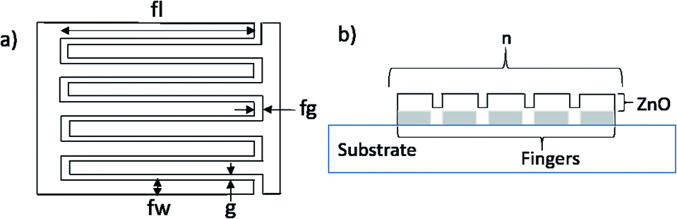 | ||
| Fig. 1 (a) Top view of interdigitated electrodes used to measure the electric impedance of ZnO films. (b) Cross section of the device. | ||
| Gap between fingers, g | 20 μm |
|---|---|
| Gap at the end of the fingers, fg | 30 μm |
| Finger width, fw | 70 μm |
| Finger length, fl | 950 μm |
| Electrode thickness | 320 nm |
| Number of fingers, n | 11 |
| Total area | 1 mm2 |
Finally, optical measurements have been performed by a UPB-150-ART Integrating sphere, to obtain the reflection spectra of grown ZnO thin films in the visible region. The optical reflection has been measured for the samples obtained in set 5 described in Table 1.
3 Results
3.1. Flow and temperature influence on the thin film deposition
ZnO thin films deposited at three different gas flow, 4, 6 and 8 L min−1, two different temperatures, 375 °C and 400 °C, and a deposition time of 1 h are analysed to study the influence of the aerosol flow on the grown thin films. Fig. 2 shows SEM images of the six samples and Table 3 summarizes the average particle size and nucleation site density.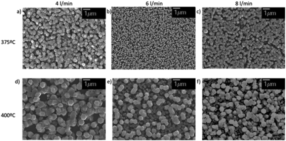 | ||
| Fig. 2 SEM images of ZnO deposited for three different flows and two different temperatures, every of them of 1 h. | ||
| (a) Average particle size (μm2) | (b) Nucleation site density (particles per μm2) | |||||
|---|---|---|---|---|---|---|
| 4 L min−1 | 6 L min−1 | 8 L min−1 | 4 L min−1 | 6 L min−1 | 8 L min−1 | |
| 375 °C | 0.11 | 0.03 | 0.08 | 5.12 | 9.31 | 4.55 |
| 400 °C | 0.61 | 0.35 | 0.44 | 3.25 | 5.96 | 3.61 |
The change of flow produces a variation in the grain size (see Table 3a). The one that provides the smallest particle size is 6 L min−1. Accordingly, the flow also produces an effect on the nucleation density (see Table 3b), reaching a maximum of 9.31 particles per μm2 for 6 L min−1 and a temperature of 375 °C. Meanwhile for 4 L min−1 and 8 L min−1 are 5.12 and 4.55 particles per μm2 respectively, which means a decrease of approximately 50 and 45% compared to the value obtained for the flow rate of 6 L min−1. For the temperature of 400 °C, the nucleation site density for the 6 L min−1 sample is 5.96 particles per μm2, while 3.25 and 3.61 particles per μm2 are grown for 4 L min−1 and 8 L min−1, which means a decrease of 45 and 40% respectively. According to these results, the smallest particle size is obtained for the process conditions of the highest nucleation site density, i.e. a flow rate of 6 L min−1 and a deposition temperature of 375 °C. Since the particle concentration in the aerosol does not vary with the flow rate (ESI†), the impact of the flow rate on nucleation site density and particle size is thought to be determined by the kinetic energy of the aerosol droplets. For a flow of 4 L min−1 the droplet velocity is not high enough to allow all droplets to arrive at the substrate due to the presence of convection currents generated by the heater located at the bottom of the chamber. In contrast, for a flow of 8 L min−1, the velocity is so high that some droplets are not adsorbed and rebound on the substrate surface. Therefore, from the thin film quality point of view, the best flow rate is 6 L min−1, since it provides the smallest particle size and the highest nucleation site density, both of which are essential for growing a homogeneous thin film. The influence of the flow in the microstructure of the ZnO is minor compared to the temperature influence (see Table 3a). Islands with different sizes are formed depending on the temperature, the higher the temperature, the larger the particle size is.
In order to further characterize the temperature dependence of the microstructure, XRD analyses have been performed on ZnO thin films grown with the parameters shown in set 2, Table 1. Fig. 3 shows the XRD patterns. The SEM images of the ZnO grown in the processes of this set are shown in Fig. 4.
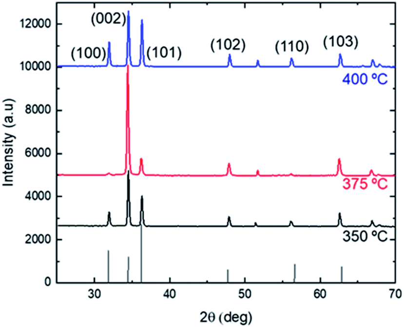 | ||
| Fig. 3 XRD image of the ZnO thin film prepared at 350 °C, 375 °C, 400 °C and flow of 6 L min−1, the deposition time has been 1 hour. The ZnO JCPDS (36-1451)25 data is presented at the bottom of the graphic for comparison. | ||
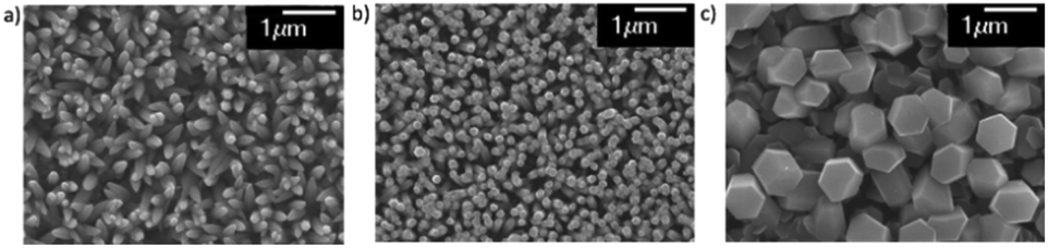 | ||
| Fig. 4 SEM images of the ZnO deposition at (a) 350 °C, (b) 375 °C and (c) 400 °C, for a flow of 6 L min−1 and 1 h of deposit. | ||
The XRD patterns of the grown ZnO confirm, in all cases, the formation of a hexagonal wurtzite structure according to the JCPDS, (36-1451).25 They exhibit, in all cases, a high intensity peak at 2θ ≈ 35°, which corresponds to (002) plane. This peak stands out especially for the film deposited at 375 °C. For the 350 °C and 400 °C patterns, the intensity of the (002) peak decrease while the intensity of the (101) peak is higher than the one obtained for 375 °C, which implies larger surface areas in the (001) plane.25Fig. 4 shows what is expected from the XRD results. A preferential crystallization of the c-axis oriented ZnO grains perpendicular to the substrate surface in the sample deposited at 375 °C (Fig. 4b) is consistent with the high intensity of (002) peak. In addition, grain growth along the c-axis minimizes the (001) plane surface,26 which is consistent with the smallest average grain size measured for the 375 °C sample. For the 350 °C deposition (Fig. 4a), some pyramidal-shape grains grow not perpendicular to substrate surface, which explains the decrease in (002) peak and the higher intensity of the (101) peak.25 As for Fig. 4c, the hexagonal shape of the grains is visible at 400 °C, but a larger grain size (longer hexagon apothem) and different orientations of growth are consistent with the decrease in (002) peak as peak (101) becomes higher. As a final remark, these results agree with previous studies showing the highest intensity peak in the ZnO (002) plane.16,27
It is worthy to compare the temperature influence on the AACVD of ZnO with other deposition approaches as PLD or ALD. The work performed by M. Liu et al., show the effect of the deposition temperature on the crystallinity and surface morphology in their PLD processes.28 The temperatures analyzed vary from 100 °C up to 500 °C showing that for the lowest temperatures there is not (002) ZnO growth which is a behaviour similar to what we obtain at temperatures lower than 325 °C. The (002) intensity peak increases with the temperature, reaching the maximum at 400 °C, that is similar to the one that provides a higher intensity peak in our work (375 °C). For 500 °C the (002) peak decreases, similarly to what happen in our case from 375 °C to 400 °C. Regarding the ALD processes performed by J. Iqbal et al., the temperature required for ZnO deposition (100–300 °C) is lower than for our AACVD depositions. The XRD analysis shows intensity peaks not only for the (002) plane but also for the (100) and (101). The deposition temperature that results in grains with a better orientation degree along the c-axis is 300 °C, which is smaller than the one that provides the better c-axis orientation for our AACVD system.
3.2. Study of microstructural evolution during ZnO film growth and growing kinetics
With the aim of studying the microstructural evolution, SEM images have been taken for a group of samples obtained in processes carried out at three different temperatures, 350 °C, 375 °C and 400 °C with 6 L min−1 constant flow, and deposition time ranging from 5 min to 1 h. As it is shown in Fig. 5, for the cases of 375 °C and 400 °C, in the first 15–20 minutes, there is a significant growth of nucleation sites. After minute 20, the number of nucleation sites decreases while particle size increases since the coalescence of islands and the formation of multi-domain islands are the principal processes. Finally, a continuous thin film is achieved after 1 hour of process. In the case of 350 °C, the average particle size is the smallest at the beginning, but it eventually will overtake the 375 °C grain size for the 1 h deposition sample due to the grains also grow along the planes (101) and (100) apart from (001). This factor facilitates the covering of the whole surface faster than the 375 °C and 400 °C cases but with the disadvantage of growing a thinner film.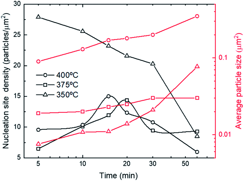 | ||
| Fig. 5 Number of nucleation points of ZnO (left axis) and average particle size (right axis) vs. deposition time for 350 °C, 375 °C and 400 °C, for a flow of 6 L min−1. | ||
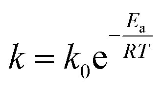
To complete the microstructural characterization, a kinetics study has been performed. In Fig. 6 the deposition rate versus the deposition temperature for samples of set 4, Table 1 is depicted. Two regions can be distinguished in the graph. From 325 °C up to 375 °C, the film growth rate increases exponentially with temperature according to an Arrhenius equation, expressed in the general form as:29,30
 | (1) |
 | ||
| Fig. 6 Logarithmic evolution of the deposition rate with respect to the inverse of the deposition temperature. | ||
For temperatures higher than 375 °C, the ZnO deposition rate remains constant, as the flat region of Fig. 6 shows. In this region, the size of the grown particles is larger than the obtained for lower temperatures. The velocity with which the reagents arrive to the regular surface now limits the film growth.
3.3. Electronic and optical characterization
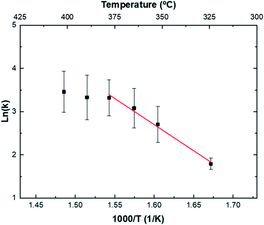
The impedance of the grown ZnO thin film, Z (f), is analyzed in the complex plane. For this study, a ZnO thin film (TF) of 1 μm of thickness has been deposited on the interdigital devices shown in Fig. 1. The impedance measurements have been performed before the ZnO deposition, after the thin film deposition, and after a thermal treatment (TT) at 700 °C during 4 h.The measurements have been performed from a frequency of 10 Hz up to 1 MHz. The data obtained is presented through a Nyquist plot, Fig. 7. An equivalent circuit is proposed in order to interpret the results, for this, the thin film is considered as an array of grains with boundaries,35 as it is depicted in Fig. 8a. Consequently, a RC parallel circuit is used to fit the conduction of carriers through the grains and other RC parallel circuit for grain boundaries. Both RC circuits are in series as Fig. 8b shows. The obtained resistance and capacitance values are shown in Table 4.
 | ||
| Fig. 7 Nyquist plot of the impedance measured for the thin films grown on the interdigitals with a thickness of 1 μm with and without thermal treatment. The inset shows the Nyquist plot of the bare interdigitals. | ||
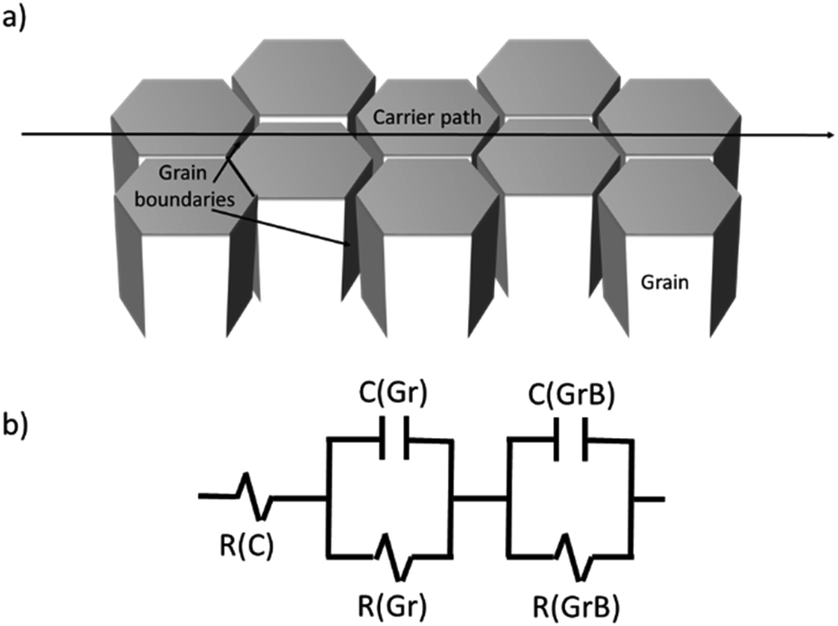 | ||
| Fig. 8 (a) Model of conduction pathway going through grains (Gr) and grain boundaries (GrB). (b) Equivalent circuit for the ZnO thin films with two RC parallel circuit in series with the contact resistance, R(C).37 | ||
| R(C) | R(Gr) | R(GrB) | C(Gr) | C(GrB) | |
|---|---|---|---|---|---|
| TF | 35 Ω | 470 kΩ | 1.5 MΩ | 6.7 × 10⁻¹¹ F | 1.3 × 10⁻⁹ F |
| TF TT | 35 Ω | 350 kΩ | 750 kΩ | 1.5 × 10⁻¹¹ F | 3.1 × 10⁻¹⁰ F |
| Bare | 35 Ω | 1.6 kΩ | 2.5 × 10⁻⁷ F |
Values of capacitance between 10−9 and 10−10 F are associated with grain boundary conduction. On the other hand, capacitances in the range of 10−12 F are associated with grain conduction.36 Regarding the resistive values, there is a slight difference in the resistance values associated with grain conduction between the sample with and without annealing, which is explained by the rearrangement of atoms during the thermal process.
On the other hand, the resistance value associated with the grain boundaries in the annealed sample is significantly lower as the annealing increases the grain size, reducing the number of grain boundaries.
Concerning the optical measurements, Fig. 9 shows the reflectance of the ZnO of the samples grown in set 5, Table 1.
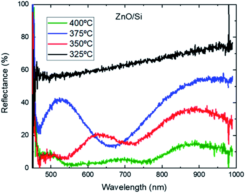 | ||
| Fig. 9 Reflectance in % of the ZnO grown with 4 different temperatures and a deposition time of 15 min, captured with an integrating sphere. | ||
The ZnO thin film grown at 325 °C shows the highest reflectance in the studied region. No peaks are observed. The measured reflectance corresponds to that of the substrate attenuated by the very thin, even discontinuous, layer of ZnO. At 350 °C, two reflection peaks are formed, around 650 nm and 900 nm. As the deposition temperature increases, the reflection peak moves from 650 towards 500 nm, as in the cases of 375 °C and 400 °C. The reflectance peak around 900 nm is present for all cases.
All these trends are also observable in the study of N. B. Khelladi et al. This variation of reflectance as a function of deposition temperature can be related to the growth kinetics and thus to the thickness of the thin film, as shown by N. B. Khelladi et al.,38 for ZnO films of three different thicknesses, 200 nm, 500 nm and 700 nm, grown with the sol–gel technique. Besides thickness, there are another aspects that may interfere in the ZnO reflection as could be the grain size and/or the carrier concentration.39 These results open the possibility of in situ monitoring of thin film growth by spectrometric analysis.
4. Conclusion
ZnO thin films have been deposited by AACVD for the study of the effect of deposition parameters as well as growth kinetics. Aerosol flow has been confirmed to slightly influence particle size. However, it is the temperature of deposition that has the greatest impact on the morphology of the grown film, as would be expected in a reaction controlled process. The morphology presents variations in the orientation planes for the studied temperatures, 350 °C 375 °C and 400 °C, but the one with a better degree of preferential orientation along the c-axis is 375 °C. The activation energy of the chemical reaction has been calculated, giving a value of 1.06 eV, which is bigger than the shown in other works for the spray pyrolysis technique. The impedance measurements are in accordance to the microstructural characterization results. The resistance term due to the grain boundaries decreases after a thermal treatment of the sample due to reduction in the number of grain boundaries. The optical characterization shows that there is a relation between the thin film thickness and the spectrographic measurements. To conclude ZnO thin film growth has some direct applications, for example as chemoresistive material for gas sensing devices. ZnO can also be an antireflective coating to improve solar cells performance. It also has applications in electro-optical devices as Light Emitting Diodes (LEDs) and spintronics.Conflicts of interest
There are no conflicts to declare.Acknowledgements
This research has been supported by EU H2020 program 767285 “Nanostencil”. We acknowledge the support of our colleagues completely necessary to perform this work.Notes and references
- S. O'Brien, M. G. Nolan, M. Çopuroglu, J. A. Hamilton, I. Povey, L. Pereira, R. Martins, E. Fortunato and M. Pemble, Thin Solid Films, 2010, 518, 4515–4519 CrossRef.
- C. W. Bunn, Proc. Phys. Soc., 1935, 47, 835–842 CrossRef CAS.
- T. Minami, Semicond. Sci. Technol., 2005, 20(4), S35–S44 CrossRef CAS.
- F. Rahman, Opt. Eng., 2019, 58, 1 Search PubMed.
- Y. Xia, L. Zhou, J. Yang, P. Du, L. Xu and J. Wang, ACS Appl. Electron. Mater., 2020, 2, 580–589 CrossRef CAS.
- V. S. Bhati, M. Hojamberdiev and M. Kumar, Energy Reports, 2020, 6, 46–62 CrossRef.
- S. J. Pearton, D. P. Norton, Y. W. Heo, L. C. Tien, M. P. Ivill, Y. Li, B. S. Kang, F. Ren, J. Kelly and A. F. Hebard, J. Electron. Mater., 2006, 35, 862–868 CrossRef CAS.
- N. Baguer, V. Georgieva, L. Calderin, I. T. Todorov, S. Van Gils and A. Bogaerts, J. Cryst. Growth, 2009, 311, 4034–4043 CrossRef CAS.
- A. Hasnaoui, O. Politano, J. M. Salazar, G. Aral, R. K. Kalia, A. Nakano and P. Vashishta, Surf. Sci., 2005, 579, 47–57 CrossRef CAS.
- S. Schmidt, G. Greczynski, C. Goyenola, G. K. Gueorguiev, Z. Czigány, J. Jensen, I. G. Ivanov and L. Hultman, Surf. Coatings Technol., 2011, 206, 646–653 CrossRef CAS.
- C. Goyenola, S. Stafström, L. Hultman and G. K. Gueorguiev, J. Phys. Chem. C, 2012, 116, 21124–21131 CrossRef CAS.
- G. Wisz, I. Virt, P. Sagan, P. Potera and R. Yavorskyi, Nanoscale Res. Lett., 2017, 12, 6 CrossRef PubMed.
- H. Li, J. Wang, H. Liu, H. Zhang and X. Li, J. Cryst. Growth, 2005, 275, 943–946 CrossRef.
- P. Boryło, K. Matus, K. Lukaszkowicz, J. Kubacki, K. Balin, M. Basiaga, M. Szindler and J. Mikuła, Appl. Surf. Sci., 2019, 474, 177–186 CrossRef.
- M. E. L. Sabino, D. M. Oliveira, V. D. Falcão, A. C. Bernardes-Silva and J. R. T. Branco, Powder Diffr., 2008, 23, S91–S93 CrossRef CAS.
- M. Krunks, T. Dedova and I. Oja Açik, Thin Solid Films, 2006, 515, 1157–1160 CrossRef CAS.
- C. E. Knapp and C. J. Carmalt, Chem. Soc. Rev., 2016, 45, 1036–1064 RSC.
- D. S. Bhachu, M. R. Waugh, K. Zeissler, W. R. Branford and I. P. Parkin, Chem.–A Eur. J., 2011, 17, 11613–11621 CrossRef CAS.
- X. Hou and K. L. Choy, Chem. Vap. Depos., 2006, 12, 583–596 CrossRef CAS.
- S. Vallejos, N. Pizúrová, J. Čechal, I. Gràcia and C. Cané, J. Vis. Exp., 2017, 1–5 Search PubMed.
- M. R. Waugh, G. Hyett and I. P. Parkin, Chem. Vap. Depos., 2008, 14, 369–372 CrossRef.
- D. B. Potter, M. J. Powell, J. A. Darr, I. P. Parkin and C. J. Carmalt, RSC Adv., 2017, 7, 10806–10814 RSC.
- A. Shukla, V. K. Kaushik and D. Prasher, Electron. Mater. Lett., 2014, 10, 61–65 CrossRef CAS.
- F. Zahedi, R. S. Dariani and S. M. Rozati, Acta Metall. Sin., 2015, 28, 110–114 CrossRef CAS.
- S. Chen, R. M. Wilson and R. Binions, J. Mater. Chem. A, 2015, 3, 5794–5797 RSC.
- S. Chen, M. McLachlan, A. Sapelkin and R. Binions, J. Mater. Chem. A, 2015, 3, 22311–22315 RSC.
- E. Bacaksiz, S. Aksu, G. Çankaya, S. Yilmaz, I. Polat, T. Kucukomeroglu and A. Varilci, Thin Solid Films, 2011, 519, 3679–3685 CrossRef CAS.
- M. Liu, X. Q. Wei, Z. G. Zhang, G. Sun, C. S. Chen, C. S. Xue, H. Z. Zhuang and B. Y. Man, Appl. Surf. Sci., 2006, 252, 4321–4326 CrossRef CAS.
- K. J. Laidler, Pure Appl. Chem., 1996, 68, 149–192 CAS.
- A. S. Patnaik and J. L. Goldfarb, Cellul. Chem. Technol., 2016, 50, 311–320 CAS.
- R. S. Sabry and D. K. H. Kafi, Int. J. Appl. Nat. Siences, 2013, 2, 29–38 Search PubMed.
- R. Ayouchi, F. Martin, D. Leinen and J. R. Ramos-Barrado, J. Cryst. Growth, 2003, 247, 497–504 CrossRef CAS.
- K. L. Choy, Prog. Mater. Sci., 2003, 48, 57–170 CrossRef CAS.
- H. Bisht, A. Mehrtens and M. A. Aegerter, Interface Control. Mater, 2000, 9, 18–23 CAS.
- L. D. Sappia, M. R. Trujillo, I. Lorite, R. E. Madrid, M. Tirado, D. Comedi and P. Esquinazi, Mater. Sci. Eng., B, 2015, 200, 124–131 CrossRef CAS.
- Y. Min, PhD in Electronic, Photonic, and Magnetic Materials, Massachusetts Institute of Technology, 2003.
- L. D. Sappia, M. R. Trujillo, I. Lorite, R. E. Madrid, M. Tirado, D. Comedi and P. Esquinazi, Mater. Sci. Eng., B, 2015, 200, 124–131 CrossRef CAS.
- N. B. Khelladi and N. E. C. Sari, Adv. Mater. Sci., 2013, 13, 799–800 Search PubMed.
- E. Ş. Tüzemen, S. Eker, H. Kavak and R. Esen, Appl. Surf. Sci., 2009, 255, 6195–6200 CrossRef.
Footnote |
| † Electronic supplementary information (ESI) available. See DOI: 10.1039/d1ra03251h |
| This journal is © The Royal Society of Chemistry 2021 |