DOI:
10.1039/D1RA02531G
(Paper)
RSC Adv., 2021,
11, 19779-19787
High performance GZO/p-Si heterojunction diodes fabricated by reactive co-sputtering of Zn and GaAs through the control of GZO layer thickness†
Received
31st March 2021
, Accepted 26th May 2021
First published on 1st June 2021
Abstract
The effect of thickness of Ga doped ZnO (GZO) layer on the performance of GZO/p-Si heterojunctions fabricated by reactive co-sputtering of Zn–GaAs target is investigated. GZO films were deposited at 375 °C with 0.5% GaAs area coverage of Zn target and 5% O2 in sputtering atmosphere. X-ray diffraction and X-ray photoelectron spectroscopy show that c-axis orientation of crystallites, Ga/Zn ratio and oxygen related defects depend substantially on the thickness of films. The 200–350 nm thick GZO films display low carrier concentration ∼1017 cm−3, which increases to >1020 cm−3 for thicker films. The diodes fabricated with >500 nm thick GZO layers display non-rectifying behaviour, while those fabricated with 200–350 nm thick GZO layers display nearly ideal rectification with diode factors of 1.5–2.5, along with, turn-on voltage ∼1 V, reverse saturation current ∼10−5 A, barrier height ∼0.4 eV and series resistance ∼200 Ω. The drastically improved diode performance is attributed to small Ga/Zn ratio (∼0.01) and extremely low dopant activation (∼0.3%), owing to diffusion and non-substitutional incorporation of Ga in thin GZO layers, which cause self-adjustment of doping concentration. These factors, together with c-axis orientation and chemisorbed oxygen at grain boundaries, facilitate ideal diode characteristics, not reported earlier for GZO/p-Si heterojunctions.
Introduction
Zinc oxide (ZnO) continues to be extensively explored for applications in several technological areas, including, photovoltaics,1 optoelectronics,2 nano-electronics3,4 and laser technology.5,6 For most of these applications, the special characteristics of ZnO, which include, a direct band gap of 3.37 eV and exciton binding energy of 60 meV, together with its resource accessibility, low cost and non-toxicity,7,8 make it a sought after material with unique advantages. Highly doped ZnO films1–3 have emerged as excellent transparent electrode materials, which care being used as alternative to tin oxide and indium–tin-oxide (ITO) for many applications, including solar cells and flat panel displays.4–6 The controlled, in situ n-doping of ZnO, however offers a viable, convenient and efficient method for fabricating devices that have immense potential for diverse applications, spanning: photo-detectors,9 sensors,10 thermoelectrics,7 catalysis,11 piezoelectric transducers,12 nanogenerators,13 field emission14 and heterojunctions.15 Substantial efforts have also been made towards stable and reproducible p-type doping of ZnO,2 particularly for the fabrication of homojunction diodes and laser diodes.16–18 Unfortunately, there have been constraints in obtaining reliable p-type ZnO with adequate carrier concentration and conductivity.2 The development of ZnO-based heterojunctions is therefore a plausible option, albeit compared to homo-junctions, the efforts in this direction have met with limited success, as seen in the cases of ZnO based piezoelectric transducers, gas sensors and solar cells.2,3 This is mainly due to the elevated energy barrier formed at the junction interface with large band offsets and barrier height inhomogeneities.7–9,19 Nonetheless, a number of efforts have been made towards the fabrication of ZnO-based heterojunctions, substituting p-type ZnO with p-type, SiC,20 Si,21 NiO,22 CuI,23 diamond,24 GaN25 and CuO.26 The n-ZnO/p-Si heterojunction diodes are specially attractive, owing to the availability and quality of crystalline silicon, as well as the possibility of hybrid integration of ZnO based devices with high density silicon technology. As a result, fabrication of n-ZnO/p-Si heterojunction diodes have been attempted by various deposition processes, such as thermal evaporation,27,28 chemical bath deposition29 magnetron sputtering30,31 pulsed laser deposition32,33 and chemical vapour deposition,34 albeit with moderate performance, resulting in diode ideality factors, usually in the range of 2–10.35–37
Owing to closeness of the ionic radii of Ga and Zn, Ga-doped ZnO (GZO) films can be obtained with minimal defects and strain38,39 and hence, are attractive for controlled doping of ZnO and fabrication of ZnO-based devices. The immense technological advantages, such as, low temperature operation, high deposition rates, uniformity and scalability, have driven the application of RF sputtering of a ZnO–Ga2O3 ceramic target for the routine deposition of GZO films.2,3,6,34,35 Being particularly suitable for device fabrication on flexible substrates, RF sputtering of a ZnO–Ga2O3 ceramic target has also been employed to fabricate ZnO-based heterojunction diodes.40–42 Interestingly, the use of reactive co-sputtering of Zn and Ga targets has been rather scarce, possibly due to the melting of Ga near room temperature, although there have been some attempts to reactively sputter a Zn–Ga alloy target in Ar–O2 atmosphere for depositing GZO films.43–45 An alternative approach has been demonstrated by our group,46 in which, the co-sputtering of Zn and GaAs in Ar–O2 atmosphere was used to grow transparent and conducting GZO films. The main advantage of this simple reactive co-sputtering approach (DC or RF) is that the doping content and stoichiometry of GZO films can be effectively manipulated by partially covering the Zn erosion track by a small piece of GaAs and controlling the oxygen percentage in Ar–O2 atmosphere.46,47 We have recently extended this technologically smart approach48 to the fabrication of n-GZO/p-Si heterojunctions. It was demonstrated that the doping and stoichiometry in GZO layer can be effectively managed to improve the performance of GZO/p-Si heterojunction, with an ease that was hitherto, not possible with sputtering of a ZnO–Ga2O3 ceramic target. This work has in particular shown that although the diode performance is controlled primarily by the Ga content of GZO layer, the behaviour of heterojunctions is significantly affected by the microstructure and oxygen related defects in GZO films, all of which are critically dependent on the oxygen partial pressure in reactive sputtering atmosphere.
The present study describes further exploration of the fabrication of n-GZO/p-Si heterojunction diodes by reactive co-sputtering of a Zn–GaAs target, with particular focus on the role of thickness of the GZO layer in determining the performance of the diode. It is well known that the microstructure and crystallinity of ZnO films are strongly thickness dependent and hence, thickness plays a significant role in determining their electrical as well as optical properties.49–52 It is usually observed that for thicknesses in the range of 100–400 nm, GZO films display substantially smaller values of carrier concentration and mobility, compared to the thicker films.50,51 There are also associated changes in the band gap and transmittance (in visible region) of the films,50–52 although for thickness approaching ∼1000 nm, the specular transmittance is substantially limited by diffused scattering due to increase in roughness, as has been reported53 for In doped ZnO films. Moreover, studies relating the thickness of GZO layer with the performance of n-GZO/p-Si heterojunctions diodes are not seen in the literature, particularly for devices fabricated by sputtering technique. Considering the important role of thickness in determining the microstructure and physical properties of GZO films, the understanding of its effect on the performance of GZO/Si devices may be essential for their optimization. In the present work, the GZO/Si heterojunctions were fabricated under identical sputtering conditions, with different thicknesses of the GZO layer between 200 nm to 850 nm, which is the typically employed range of thickness for various opto-electronic applications. The structure, composition and the electrical/optical properties of the GZO films of different thicknesses have been investigated to evaluate the thickness dependent changes associated with Ga doping level in the GZO layer and its microstructure. The behavior and performance of the GZO/p-Si heterojunctions have been investigated and the diode parameters have been correlated with the doping level of Ga and the microstructure and oxygen related defects in the GZO layer. Our results show that the diode performance is strongly dependent on the thickness of GZO layer, which displays self-adjustment of the doping level in the vicinity of GZO/Si interface, leading to the formation of nearly ideal diode heterojunctions with thin GZO layers.
Experimental
GZO films were deposited on quartz and p-Si wafer 〈100〉 (about, 1 cm × 1 cm size and carrier concentration ∼1015 cm−3) by reactive RF magnetron sputtering of a Zn target in Ar–O2 mixture by partially covering a zinc (99.99%) target with a piece of GaAs, as described elsewhere47,48 and also shown as Fig. S1, in section A of ESI.† Prior to deposition, the substrates have been cleaned with ultrasonic rinsing with de-ionized water, acetone, and propanol and finally degreased in propanol vapor. The RF power was fixed at 400 W and the deposition was carried out at a gas pressure of ∼2 Pa and substrate temperature of ∼375 °C. The oxygen partial pressure was fixed at ∼0.10 Pa which corresponds to 5% O2 in a sputtering atmosphere. The deposition time were varied from 15 min to 60 min to deposit GZO films of different thicknesses in the range of (200–850) nm. The thickness of the films deposited on quartz substrate was measured from the interference patterns in their transmittance spectra. Powder X-ray diffraction (XRD) measurements were carried out by a high-resolution X-ray diffractometer in ω–2θ mode, using a RIGAKU-Smart Lab-X-ray diffractometer, equipped with a 9 kW Cu rotating anode X-ray source. The resistivity, carrier concentration and mobility of the films were measured at room temperature by van der Pauw's method, using a Lake Shore 8400 series Hall system. X-ray photoelectron spectroscopy (XPS) was performed with Kratos analytical Axis Supra ESCA instrument, equipped with monochromatic Al Kα (1486.6 eV) source. The XPS measurements were made after surface cleaning with 2 keV Ar+ ions for 2–3 min. All the peaks were corrected for charging with reference to C 1s peak (284.8 eV). The Shirley type function was used to fit the background signal and the peaks were fitted with a combination of Gaussian and Lorentzian line shapes, using ESCApe software.
Results
Structure and morphology
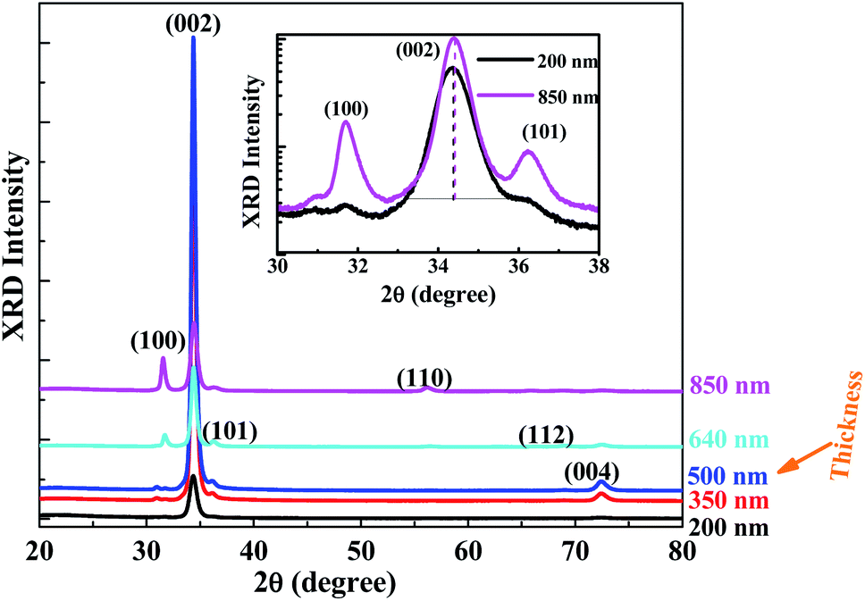
Fig. 1 shows the powder XRD patterns of GZO films of different thicknesses. All the films display diffraction peaks corresponding to wurtzite ZnO (JCPDS file 36-1451), dominated by the (002) peak, indicating strong c-axis preferred orientation of crystallites. No XRD peaks due to GaAs or elemental Zn, Ga and As were seen in any of the films. For the purpose of comparison, the typical XRD pattern of a GZO film deposited by sputtering of a composite ZnO–Ga2O3 target is shown as Fig. S2 in section B of ESI.† The 200 nm thick film shows the presence of (100) and (101) peaks as weak shoulders to the dominant (002) and (004) peaks, indicating nearly complete c-axis orientation of crystallites. With increase of thickness, the (100) reflection acquires more prominence and a monotonous increase in the intensity ratio of (100) to (002) peaks (I(100)/I(002)) is seen. However, the films with thickness above 500 nm show multiple peaks due to (100), (101), (110), (112) and (201) reflections, indicating enhanced misorientation of crystallites, compared to the films with smaller thickness. The value of lattice constant, c was found to be 5.219 Å for the 200 nm thick films, which tends to decrease slightly with increase of thickness, attaining a value of 5.213 Å for the 850 nm thick films.
 |
| | Fig. 1 X-ray diffraction patterns of GZO films of different thicknesses; inset shows the logarithmic plot for the films with the lowest and highest thicknesses. | |
The standard c value for hexagonal ZnO is 5.2066 Å, hence, all the films display tensile strain ∼10−3 along c-axis, which decreases slightly with increase of thickness. The tensile strain along c-axis may be attributed to the possible incorporation of excess/interstitial oxygen in the films, since the substitutional doping of Ga in ZnO lattice is expected to produce a compressive hydrostatic strain,9 as the radius of Ga3+ ion is smaller than that of Zn2+ ion. The crystallite size along c-axis was obtained from the FWHM of (002) peak for all the films. The 200 nm thick film exhibited crystallite size of ∼20 nm which decreased slightly to the range of (10–15) nm for thicker films.
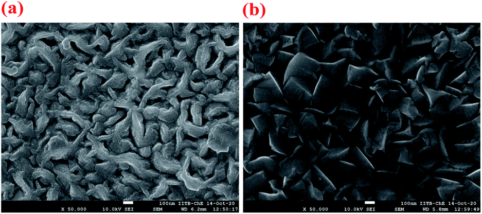
The typical FESEM images of GZO films deposited on Si are shown in Fig. 2. The surface morphology of the lower thickness film (∼200 nm) shows anisotropic lateral features, due to the formation of needle like, elongated agglomerates on the surface. In contrast, the 850 nm thick film displays a rough surface morphology, consisting of facetted and nearly equiaxed grains, similar to those reported earlier for sputtered ZnO films grown in the substrate temperature range of 300–400 °C.54
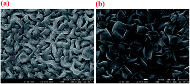 |
| | Fig. 2 FESEM images of (a) 200 nm and (b) 850 nm thick GZO films deposited on Si (bar size is 100 nm). | |
Optical transmittance
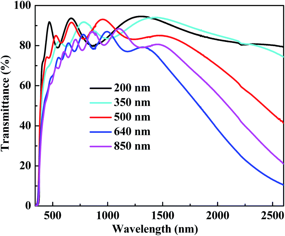
The specular transmittance spectra of GZO films are shown in Fig. 3. All the films display high transmittance with interference features in the visible region, indicating their good optical quality, along with sharp absorption edges. With increase of thickness, the average visible transmittance gradually reduces, due to increase of sub-band gap absorption in the range of 400–500 nm and scattering losses in the visible region, possibly owing to increase in surface roughness. GZO films of thickness larger than ∼500 nm also display substantial decrease of transmittance in near infrared region due to free carrier absorption and the onset of plasma resonance, which is attributed to their higher carrier concentrations, as will be seen below.
 |
| | Fig. 3 Specular transmittance of GZO films of different thicknesses. | |
Hall measurement and resistivity
The electrical parameters of typical GZO films have been obtained by Hall and resistivity measurements and the dependences of resistivity, carrier concentration and mobility on the thickness of GZO films are shown in Fig. 4. The 200 nm and 350 nm thick GZO films were found to have resistivities in the range of 20–50 Ω cm, which decreased drastically to ∼10−3 Ω cm for the thicker films. All the films displayed n-type behaviour and the large decrease of resistivity with increase of film thickness is due to the substantial increase of carrier concentration as well as mobility. Interestingly, the 350 nm thick film displays a carrier concentration of ∼6.4 × 1017 cm−3 which jumps to ∼2 × 1020 cm−3 for the 500 nm thick films and remains unchanged with further increase of thickness. The mobility also displays a large and monotonous increase from ∼0.5 cm2 V−1 s−1 to ∼24.1 cm2 V−1 s−1 as the thickness increases from 350 nm to 850 nm. Hall mobility cannot be measured for 200 nm GZO film because of high resistivity. The large increase of carrier concentration with film thickness is consistent with the free carrier effects seen in transmittance spectra of the films in the infrared region (Fig. 3), which showed substantial free carrier absorption only for 500 nm or thicker GZO films.
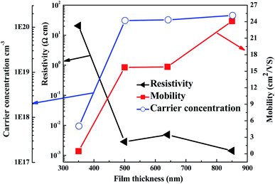 |
| | Fig. 4 Dependence of resistivity, carrier concentration and mobility of GZO on film thickness. | |
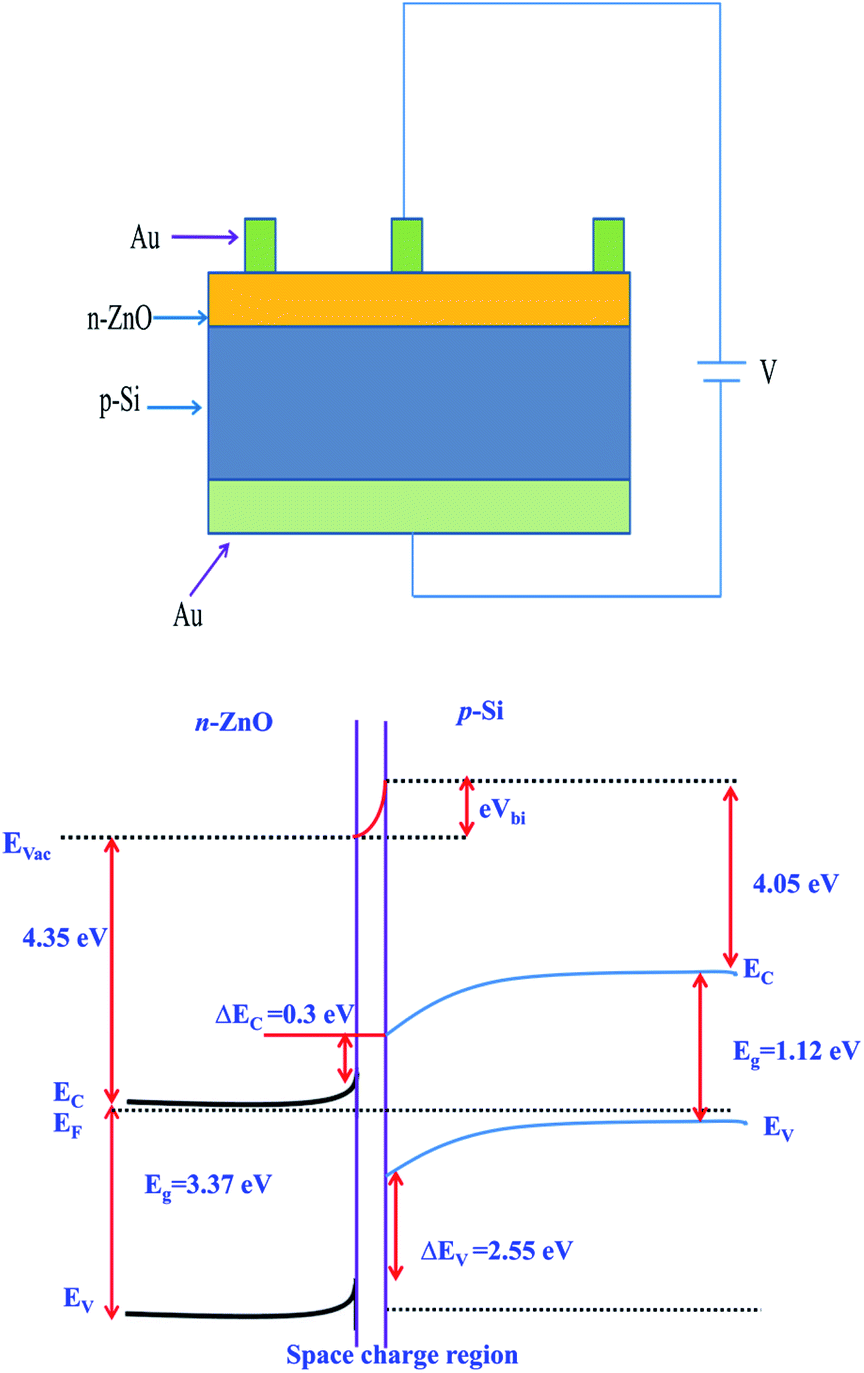
Junction characterization
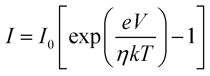
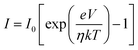
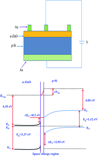
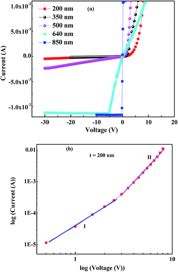
The n-GZO/p-Si heterojunction diode is schematically shown in Fig. 5(a). The corresponding energy band diagram (following the Anderson model55) is shown in Fig. 5(b) for low carrier concentration GZO layer. The band gaps (Eg) of ZnO and Si are respectively taken as 3.37 eV and 1.12 eV and the respective electron affinities (χ) as 4.35 eV and 4.05 eV. As shown in Fig. 4(b), the conduction and valence band offsets, given respectively by ΔEC (=χ(ZnO) − χ(Si)) and ΔEV (=Eg(ZnO) − Eg(Si) + ΔEC), are 0.3 eV and 2.55 eV. The I–V characteristics of the heterojunctions fabricated with GZO films of different thicknesses were obtained in planar electrode geometry, and are shown in Fig. 6(a). The I–V characteristics of the junctions formed with 200 nm and 350 nm thick GZO films show typical rectifying behavior, while the junctions formed with 500 nm thick film shows poorer rectification. On the contrary, the junctions formed with thicker GZO films exhibit nearly ohmic I–V characteristics, representing non-rectifying behavior. For the heterojunctions displaying rectifying I–V characteristics, the diode parameters were obtained from I–V characteristics and are presented in Table 1. For the purpose of comparison with contemporary literature, Table S1 of ESI† (section C) presents the reported diode parameters for ZnO/Si heterojunctions fabricated by different processes. It is seen from Table 1, that the turn-on-voltage is nearly 1 V for all the diodes, which is comparable to the reported values of 1–3 V (Table S1†) for GZO/p-Si heterojunctions.56,57 The values of reverse saturation current (measured at −10 V) are found to be in the range of (1.2–1.5) × 10−5 A for all the diodes, which is also in agreement with the reported results (Table S1†) for GZO/p-Si heterojunctions.56,57 The ideality factors (η) of the heterojunction diodes were obtained from:55| |
 | (1) |
where, e is the electronic charge, k is the Boltzmann's constant, I0 is the temperature-dependent reverse saturation current, η is the ideality factor and T is absolute temperature. By using the conventional approach,58 the parameters η and I0 were estimated from the ln(I) vs. V dependence at room temperature. The variation of the ideality factor (η) of n-GZO/p-Si diodes with the thickness of GZO layer is shown in Table 1. The value of η for the diode fabricated with 500 nm thick GZO layer is 12. It changed drastically to 2.5, for the diode fabricated with 350 nm thick GZO layer and improved further to 1.5, with decrease of thickness to 200 nm. It is noted from Table S1† that the values of diode ideality factor for GZO/p-Si heterojunctions fabricated by different deposition techniques are usually reported in the range of 2–10.35,36,56,57,59 In comparison, our results show that the GZO/p-Si heterojunction diodes fabricated with GZO layer thickness in the range of 200 to 350 nm, display close to ideal behavior with diode factors in the range of 1.5–2.5. These values of diode factor appear highly promising for various device applications, particularly considering the technological versatility and scalability of reactive sputtering technique as a growth process at moderate substrate temperatures.
 |
| | Fig. 5 The schematic structure of n-GZO/p-Si heterojunction diode along with the energy band diagram for lightly doped n-GZO/p-Si heterojunction. | |
 |
| | Fig. 6 (a) Room temperature I–V characteristics of heterojunctions fabricated with GZO layers of different thicknesses (b) the log(I) vs. log(V) graph in forward bias, for the heterojunction diode employing 200 nm thick GZO layer. | |
Table 1 Diode parameters of GZO/p-Si heterojunctions fabricated with GZO layers of different thicknesses
| Thickness (nm) |
Turn on voltage (V) |
Reverse bias current (at −10 V) (A) |
Ideality factor (η) |
Barrier height (eV) |
Series resistance (Ω) |
| 200 |
1.0 |
1.22 × 10⁻⁵ |
1.5 |
0.47 |
287 |
| 350 |
1.0 |
1.48 × 10⁻⁵ |
2.5 |
0.39 |
217 |
| 500 |
0.8 |
1.54 × 10⁻⁵ |
12 |
2.0 |
130 |
In order to evaluate the barrier height (φB) of the diode, the function H(I) is defined as60
| |
 | (2) |
and
where
A* is the Richardson constant (the value
A*
![[thin space (1/6-em)]](https://www.rsc.org/images/entities/char_2009.gif)
for p-type Si being
32 A cm
−2 K
−2). The linear plot of
H(
I)
versus I gives the
y-axis intercept as
ηφB. The value of
φB was found to be 2.0 eV for the diode fabricated with 500 nm thick GZO film, which decreased substantially to the range of (0.39–0.47) eV for (200–350) nm thick GZO films. The values of barrier height for GZO/p-Si diodes are usually reported (Table S1
†) in the range of (0.50–1.021) eV.
30,56,57 The series resistance (
Rs) is also an important factor for the application of heterojunction diodes, which can be determined from the downward curvature (nonlinear portion) of the forward bias
I–
V characteristics. Following this method,
61 the relation connecting
I and
Rs is
| |
 | (4) |
where,
IRs is the potential drop across the diode. This equation can be restructured as
| |
 | (5) |
in which, the slope of
Y(
I)
vs. I gives the value of
Rs.
The measured values of Rs are also listed in Table 1 and are found to be in the range of (100–300) Ω for the diodes fabricated with 200 nm to 500 nm thick GZO layer. These values compare well with the reported values (Table S1†) of Rs (400 Ω to 60 kΩ) for GZO/p-Si diodes.56,57 Fig. 6(b) shows the logI–logV graph in forward bias for the n-GZO/p-Si diode fabricated with 200 nm thick GZO layer. The plot displays two distinct linear parts, corresponding to different conduction mechanisms. The lower voltage region represents non-rectifying character with transition voltage at ∼0.5 V. At higher voltages, the current increases exponentially, following I ∼ exp(αV), which has been usually attributed to thermionic emission in wide band gap p–n junctions.62,63
X-ray photoelectron spectroscopy
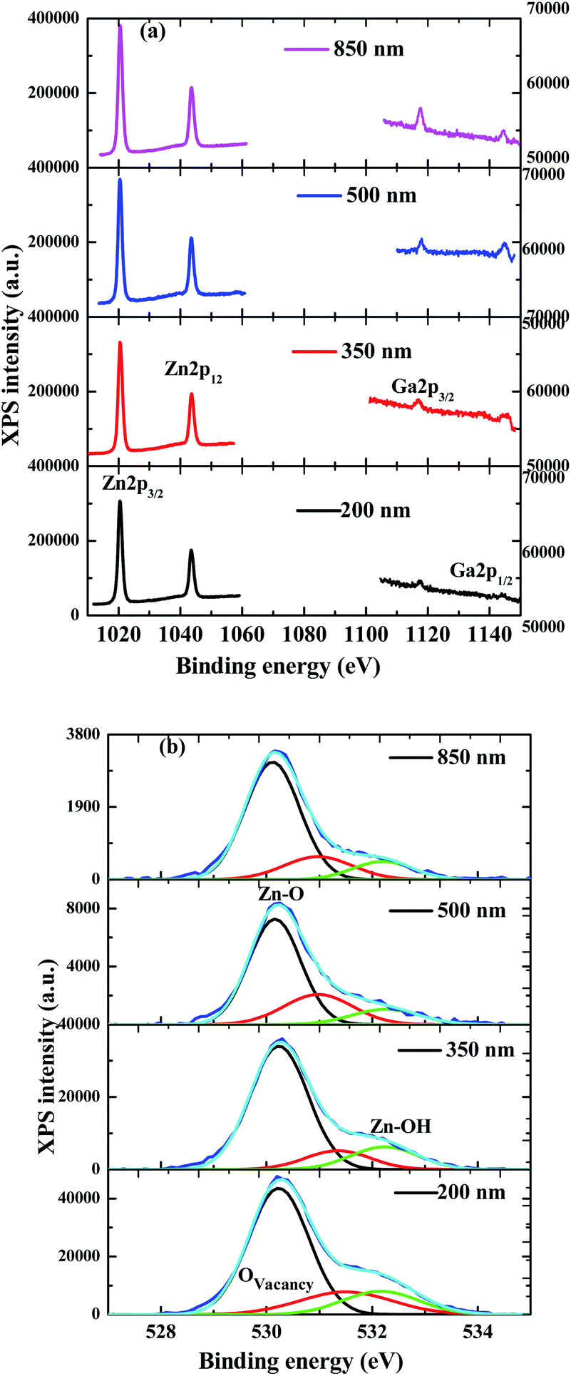
XPS studies have been carried out to understand the strong thickness dependences of the electrical parameters of GZO films and the diode behavior of GZO/Si junctions. The XPS survey scans showed that Zn, O and Ga are present in all the GZO films. Traces of As impurity were also seen, but well below the atomic concentrations of dopant Ga atoms, as expected due to the high vapour pressure of As at the growth temperature and reported earlier.47 The high resolution spectra of GZO films of different thicknesses are presented in Fig. 7(a), showing the Zn 2p and Ga 2p core level peaks. The appearance of Zn 2p3/2 peak in the range of 1021.7–1022.4 eV indicates the presence of Zn2+ state,64,65 while that of Ga 2p3/2 peaks in the range of 1118.0–1118.1 eV indicates the presence of Ga3+ state in the films.66,67 The Ga/Zn ratios were obtained from XPS data and are given in Table 2 for all the films. It is seen that with increase of film thickness from 200 nm to 500 nm, the Ga/Zn ratio increases significantly from ∼0.003 to ∼0.007. However, with further increase of film thickness to 640 nm, the Ga/Zn ratio increases to ∼0.012 and remains nearly the same for the 850 nm thick film, thus displaying saturation behaviour. The larger incorporation of Ga in thicker films explains the reduction of tensile strain and possibly, the increased misorientation and slight decrease in the size of crystallites. It is, however noteworthy that the incorporation of Ga in GZO films of lower thickness is significantly smaller. As mentioned above, the XPS spectra were recorded after surface cleaning; hence the differences in Ga/Zn ratio of the films of different thicknesses are representative of changes in the bulk and not only at the surface. Thus, the significantly smaller Ga/Zn ratio seen in 500 nm or lower thickness films is attributed to the possible loss of Ga by diffusion into SiO2/Si, owing to its high diffusivity.68
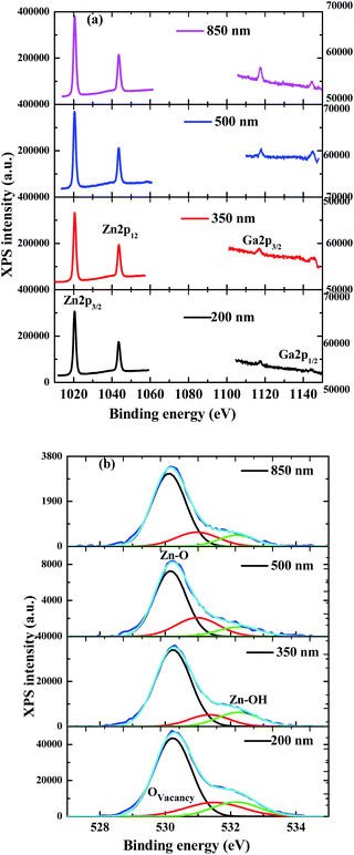 |
| | Fig. 7 (a) Zn 2p and Ga 2p, and (b) the peak-fitted O 1s core level spectra of GZO films of different thicknesses. | |
Table 2 Ga/Zn ratio and activation efficiency (%) of Ga in GZO films of different thicknesses
| Thickness (nm) |
Ga/Zn |
Activation efficiency (%) |
| 200 |
0.0026 |
— |
| 350 |
0.0050 |
0.3 |
| 500 |
0.0071 |
25.6 |
| 640 |
0.0120 |
30.4 |
| 840 |
0.0121 |
37.6 |
The chemical state of oxygen incorporated in the films of different thicknesses was also analyzed by XPS. Fig. 7(b) presents the O 1s core level peaks for GZO films, displaying asymmetric shapes. These peaks were deconvoluted and fitted by three component peaks, centered at ∼530 eV (OI), ∼531 eV (OII) and ∼532 eV (OIII). The OI component is due to the O2− state in ZnO lattice,47 while the OII component is associated with the O2− ions in oxygen deficient regions of ZnO, implying the presence of oxygen vacancies.47,67–70 It is found that the OII component remains practically unchanged in the GZO films of different thicknesses. The higher binding energy, OIII component, which appears in the range of 532.2–532.6 eV, has been usually associated with chemisorbed oxygen/hydroxyl species at the surface66 and grain boundaries.69 It is noticed that the OIII component is slightly stronger in the films of lower thickness, which may be indicative of increased oxygen chemisorptions at the grain boundaries.
Discussions
The radically different behaviors of heterojunctions formed with GZO layers of thicknesses lower and higher than ∼500 nm, can be understood in the light of the changes in structure, chemical composition and consequently the electrical/optical properties of GZO films that take place with thickness. The Ga/Zn ratios and the measured carrier concentrations were used to obtain the Ga activation efficiency (%) in films of different thicknesses and these values are also listed in Table 2. The Ga/Zn ratio in the thicker films (640 nm and 850 nm) is ∼0.012, which implies a dopant concentration of ∼4.8 × 1020 cm−3, assuming substitutional doping. The corresponding Ga activation efficiency in these films is in the range of (30–37)%, which is not far from the reported dopant activation efficiencies of 30–50% in doped ZnO.47 The large carrier concentration (≳1020 cm−3) in thicker films is thus suggestive of the efficient substitution of Ga in ZnO lattice and negligible compensating effect due to the minute presence of As impurity. Interestingly, Table 2 shows that the dopant activation efficiency decreases with decreasing thickness and the observed carrier concentration of 350 nm thick films (∼7 × 1017 cm−3) implies a dopant activation efficiency of just about 0.3%. Although the carrier concentration of the 200 nm thick film could not be measured, its significantly higher resistivity compared to the 350 nm thick film suggests that its dopant activation efficiency may even be smaller.
The above results show that the substantially smaller carrier concentration of thin GZO layers are not only due to the lower Ga/Zn ratio, but more importantly, due to the drastically smaller dopant activation efficiency, which is suggestive of non-substitutional incorporation of Ga in the thinner GZO layers. Earlier XPS studies of sputtered GZO films of thickness ∼100 nm, by Gabás et al.71 have revealed that the GZO/Si interface consists of silicon oxides, zinc silicates and some metallic Zn, as well as a small quantity of metallic Ga. They have also demonstrated by impedance spectroscopy measurements that the GZO/Si interface is less resistive than that of undoped ZnO/Si, due to Ga intrusion in the interface, making the charge transport across it, less hindered.71 It is also known that non-stoichiometric GaxOy phases can be formed during the sputtering of Ga2O3 films, leading to a wide range of oxygen substoichiometry72 and there is also a possibility of forming ZnGa2O4 phase.73,74 Another possibility is the strong compensation due to the formation of acceptor complexes, such as, (GaZn + Oi) and (AlZn + Oi),75–77 respectively reported in Ga and Al doped ZnO films, grown under O-rich conditions. A recent X-ray absorption study of reactively sputtered GZO films from our group47 has shown that the formation of (GaZn + Oi) acceptor complex depends critically on the availability oxygen during sputtering. As a consequence, the carrier concentration and mobility of these films decrease drastically with increase of O2 percentage in sputtering atmosphere in a very narrow range of 5% to 6%.47 In view of the above possibilities, it is inferred that one or more of these factors are responsible for the drastic loss of active Ga in the vicinity of GZO/Si interface, which could partly be caused by the availability of excess oxygen at the Si substrate. In any case, the net result is a severe reduction of carrier concentration, the effect of which is seen more prominently in the thinner GZO layers.
It is clear from above that the doping level in GZO layer plays the most crucial role in the formation of an ideal n-GZO/p-Si heterojunction diode. At higher thicknesses, the larger Ga/Zn ratio and efficient Ga doping result in substantially enhanced carrier concentration and conductivity of the GZO films. The GZO layer with higher electrical conductivity forms a non-rectifying contact between with p-Si, causing significant deviation from diode behavior. In the case of the devices formed with thinner GZO layers, the loss of dopant Ga and its inactivation in the vicinity of the GZO/Si interface, due to reasons explained above, causes a substantial reduction of carrier concentration in the active GZO layer, and is mainly responsible for the formation heterojunction diodes with much improved rectifying behavior. It appears that a proper choice of the thickness of GZO layer results in the self-adjustment of active Ga, leading to optimized doping concentration, suitable for the formation of ideal heterojunction diodes. It is also noted that the GZO films deposited with lower thicknesses display slightly larger crystallites and nearly complete orientation of crystallites along c-axis. This may further facilitate reduction in recombination losses at the junction interface, leading to improvement in diode characteristics. Furthermore, the films of lower thickness possess slightly higher chemisorbed oxygen/hydroxyl species, which are likely to be at the grain boundaries and may passivate defects, resulting in reduced carrier trapping. Our results show that there is a strong thickness dependence of the chemical composition of reactively sputtered GZO layer, in particular, the Ga concentration and the chemical state of oxygen, both of which critically influence the heterojunction diode performance. These factors appear to contribute towards the high performance of GZO/Si heterojunction diodes, particularly seen in the case of the GZO/p-type Si heterojunction fabricated with a 200 nm thick GZO layer, which displays nearly ideal diode behavior.
Conclusion
The role of GZO layer thickness in optimizing the performance of n-GZO/p-Si heterojunction diodes has been investigated in this work, in which, GZO was deposited by RF reactive magnetron co-sputtering of a Zn–GaAs target at 375 °C and 5% O2 in Ar–O2 atmosphere. The junctions formed with larger than 500 nm thick GZO layers do not display rectifying behaviour, primarily due to the high carrier concentration (>1020 cm−3) of these films. The heterojunctions fabricated with GZO films of 500 nm or lesser thickness, deposited under the same growth conditions, display significantly improved diode characteristics. In particular, the diodes fabricated with 200 nm and 350 nm thick GZO layers display nearly ideal diode factors of 1.5 and 2.5, respectively. These diodes display turn-on voltages ∼1 V, reverse saturation current ∼10−5 A, barrier heights ∼0.4 eV and series resistance in the range of 100–200 Ω. The drastic improvement in the diode performance is primarily attributed to substantially smaller Ga/Zn ratio in thin GZO layers, possibly due to the diffusion of Ga into SiO2/Si and extremely low dopant activation efficiency (∼0.3%), compared to thicker films, which leads to a drastic decrease of carrier concentration to ∼1017 cm−3. These factors appear to cause self-adjustment of the doping concentration in the GZO layer, if its thickness is appropriately chosen. In addition, better crystallite orientation along c-axis and larger presence of chemisorbed oxygen/hydroxyl species in thin GZO layers may also cause the passivation of defects at junction interface and reduced recombination losses, facilitating the nearly ideal diode behaviour, not reported earlier for GZO/p-Si heterojunction system. It is thus inferred that the strong thickness dependence of the performance of GZO/Si diode is rooted essentially, in the chemical composition of the reactively sputtered GZO layer, in particular, the Ga dopant concentration and the chemical state of oxygen. The diode parameters reported here, are highly promising and demonstrate that a careful manipulation of the thickness of GZO layer deposited by reactive sputtering can be efficiently utilized to optimize the performance of these devices for various applications.
Conflicts of interest
There are no conflicts to declare.
Acknowledgements
Hall Measurement Central Facility, Central Surface Analytical Facility and HRXRD Central Facility of IIT Bombay are acknowledged for Hall, XPS and XRD measurements, respectively. The authors thank M. Monish for electrical and optical measurements and helpful discussions.
Notes and references
- M. A. Zimmler, T. Voss, C. Ronning and F. Capasso, Appl. Phys. Lett., 2009, 94, 241120 CrossRef.
- Y. S. Choi, J. W. Kang, D. K. Hwang and S. J. Park, IEEE Trans. Electron Devices, 2010, 57, 26–41 CAS.
- A. B. Djuriic, A. M. C. Ng and X. Y. Chen, Prog. Quantum Electron., 2010, 34, 191–259 CrossRef.
- Z. L. Wang, Appl. Phys. A: Mater. Sci. Process., 2007, 88, 7–15 CrossRef CAS.
- V. I. Klimov, A. A. Mikhailovsky, S. Xu, A. Malko, J. A. Hollingsworth, C. A. Leatherdale, H.-J. Eisler and M. G. Bawendi, Science, 2000, 290, 314–317 CrossRef CAS PubMed.
- T. D. Krauss, Nature, 2007, 447, 385–386 CrossRef CAS PubMed.
- K. Ellmer, Nat. Photonics, 2012, 6, 809–817 CrossRef CAS.
- Ü. Özgür, Y. I. Alivov, C. Liu, A. Teke, M. A. Reshchikov, S. Doğan, V. Avrutin, S. J. Cho and H. Morkoçd, J. Appl. Phys., 2005, 98, 041301 CrossRef.
- H. Kind, H. Yan, B. Messer, M. Law and P. Yang, Adv. Mater., 2002, 14, 158 CrossRef CAS.
- Z. L. Wang, Mater. Today, 2004, 7, 26–33 CrossRef CAS.
- S. R. Kelly, X. Shi, S. Back, L. Vallez, S. Y. Park, S. Siahrostami, X. Zheng and J. K. Nørskov, ACS Catal., 2019, 9, 4593–4599 CrossRef CAS.
- D. C. Look, Mater. Sci. Eng., B, 2001, 80, 383–387 CrossRef.
- C. L. Hsu and K. C. Chen, J. Phys. Chem. C, 2012, 116, 9351 CrossRef CAS.
- Y. K. Tseng, C. J. Huang, H. M. Cheng, I. N. Lin, K. S. Liu and I. C. Chen, Adv. Funct. Mater., 2003, 13, 811 CrossRef CAS.
- Y. W. Heo, Y. W. Kwon, Y. Li, S. J. Pearton and D. P. Norton, Appl. Phys. Lett., 2004, 84, 3474 CrossRef CAS.
- K.-K. Kim, H.-S. Kim, D.-K. Hwang, J.-H. Lim and S.-J. Park, Appl. Phys. Lett., 2003, 83, 63 CrossRef CAS.
- A. Tsukazaki, A. Ohtomo, T. Onuma, M. Ohtani, T. Makino, M. Sumiya, K. Ohtani, S. F. Chichibu, S. Fuke, Y. Segawa, H. Ohno, H. Koinuma and M. Kawasaki, Nat. Mater., 2005, 4, 42 CrossRef CAS.
- W. S. Noh, J. A. Lee, J. H. Lee, Y. W. Heo and J. J. Kim, Ceram. Int., 2016, 42, 4136–4142 CrossRef CAS.
- H. Y. Kim, J. H. Kim, M. O. Park and S. Im, Thin Solid Films, 2001, 398–399, 93–98 CrossRef CAS.
- M. Guziewicz, R. Schifano, E. Przezdziecka, J. Z. Domagala, W. Jung, T. A. Krajewski and E. Guziewicz, Appl. Phys. Lett., 2015, 107, 101105 CrossRef.
- G. Akgul, F. A. Akgul, H. E. Unalan and R. Turan, Philos. Mag., 2016, 96, 1093–1109 CrossRef CAS.
- S. Y. Tsai, M. H. Hon and Y. M. Lu, Solid-State Electron., 2011, 63, 37–41 CrossRef CAS.
- F.-L. Schein, H. V. Wenckstern and M. Grundmann, Appl. Phys. Lett., 2013, 102, 092109 CrossRef.
- J. Huang, L. J. Wang, K. Tang, J. J. Zhang, Y. B. Xia and X. G. Lu, Appl. Surf. Sci., 2012, 258, 2010–2013 CrossRef CAS.
- T. A. Krajewski, P. Stallinga, E. Zielony, K. Goscinski, P. Kruszewski, L. Wachnicki, T. Aschenbrenner, D. Hommel, E. Guziewicz and M. Godlewski, J. Appl. Phys., 2013, 113, 194504 CrossRef.
- F. A. Akgul, G. Akgul, R. Turan and H. E. Unalan, J. Am. Ceram. Soc., 2016, 99, 2497–2503 CrossRef.
- W. I. Park, G. C. Yi, J. W. Kim and S. M. Park, Appl. Phys. Lett., 2003, 82, 4358 CrossRef CAS.
- T. L. Tansley and S. J. T. Owen, J. Appl. Phys., 1984, 55, 454 CrossRef CAS.
- S. Paul, J. Sultanaa, A. Bhattacharyya, A. Karmakar and S. Chattopadhyay, Optik, 2018, 164, 745–752 CrossRef CAS.
- F. Chaabouni, M. Abaab and B. Rezig, Superlattices Microstruct., 2006, 39, 171–178 CrossRef CAS.
- D. Song, D.-H. Neuhaus, J. Xia and A. G. Aberle, Thin Solid Films, 2002, 422, 180 CrossRef CAS.
- S. Majumdar and P. Banerji, J. Appl. Phys., 2009, 105, 043704 CrossRef.
- H. Qi, Q. Li, C. Wang, L. Zhang and L. Lv, Vacuum, 2007, 81, 943 CrossRef CAS.
- P. Hazra, S. K. Singh and S. Jit, J. Semicond. Sci. Technol., 2014, 14, 117–123 CrossRef.
- J. D. Lee, C. Y. Park, H. S. Kim, J. J. Lee and Y. G. Choo, J. Phys. D: Appl. Phys., 2010, 43, 365403 CrossRef.
- S. Aksoy and Y. Caglar, Superlattices Microstruct., 2012, 51, 613–625 CrossRef CAS.
- G. C. Park, S. M. Hwang, J. H. Lim and J. Joo, Nanoscale, 2014, 6, 1840 RSC.
- S. H. Chang, H. M. Cheng, C. L. Tien, S. C. Lin and K. P. Chuang, Opt. Mater., 2014, 38, 87–91 CrossRef CAS.
- K. Ellmer and A. Bikowski, J. Phys. D: Appl. Phys., 2016, 49, 413002 CrossRef.
- P. Mondal and D. Das, Appl. Surf. Sci., 2013, 286, 397–404 CrossRef CAS.
- P. K. Song, M. Watanabe, M. Kon, A. Mitsui and Y. Shigesato, Thin Solid Films, 2002, 411, 82–86 CrossRef CAS.
- C. E. Kim, P. Moon, S. Kim, J.-M. Myoung, H. W. Jang, J. Bang and I. Yun, Thin Solid Films, 2010, 518, 6304–6307 CrossRef CAS.
- Q.-B. Ma, Z.-Z. Ye, H.-P. He, L.-P. Zhu, W.-C. Liu, Y.-F. Yang, L. Gong, J.-Y. Huang, Y.-Z. Zhang and B.-H. Zhao, J. Phys. D: Appl. Phys., 2008, 41, 055302 CrossRef.
- X. Bie, J. G. Lu, L. Gong, L. Lin, B. H. Zhao and Z. Z. Ye, Appl. Surf. Sci., 2009, 256, 289–293 CrossRef CAS.
- Q.-B. Ma, Z.-Z. Ye, H.-P. He, L.-P. Zhu, J.-R. Wang and B.-H. Zhao, Mater. Lett., 2007, 61, 2460–2463 CrossRef CAS.
- D. Singh, S. Singh, U. Kumar, R. S. Srinivasa and S. S. Major, Thin Solid Films, 2014, 555, 126–130 CrossRef CAS.
- S. K. Appani, A. K. Yadav, D. S. Sutar, S. N. Jha, D. Bhattacharyya and S. S. Major, Thin Solid Films, 2020, 701, 137966 CrossRef CAS.
- P. Mondal, S. K. Appani, D. S. Suta and S. S. Major, J. Mater. Sci.: Mater. Electron., 2021, 32, 4248–4257 CrossRef CAS.
- T. Yamada, A. Miyake, S. Kishimoto, H. Makino, N. Yamamoto and T. Yamamoto, Appl. Phys. Lett., 2007, 91, 051915 CrossRef.
- X. Yu, J. Ma, F. Ji, Y. Wang, C. Cheng and H. Ma, Appl. Surf. Sci., 2005, 245, 310–315 CrossRef CAS.
- S. Liang and X. Bi, J. Appl. Phys., 2008, 104, 113533 CrossRef.
- Q. Huang and X. Bi, J. Appl. Phys., 2013, 113, 053702 CrossRef.
- S. Major and K. L. Chopra, Sol. Energy Mater., 1988, 17(5), 319–327 CrossRef CAS.
- R. Nandi and S. S. Major, Appl. Surf. Sci., 2017, 399, 305–312 CrossRef CAS.
- R. L. Anderson, IBM J. Res. Dev., 1960, 4, 283 CAS.
- H. M. Chiu, Y. T. Chang, W. W. Wu and J. M. Wu, ACS Appl. Mater. Interfaces, 2014, 6, 5183–5191 CrossRef CAS PubMed.
- N. F. Koksal, M. Sbeta, A. Atilgan and A. Yildiz, Phys. B, 2021, 600, 412599 CrossRef CAS.
- A. Drici, G. Djeteli, G. Tchangbedji, H. Derouiche, K. Jondo, K. Napo, J. C. Bernède, S. Ouro-Djobo and M. Gbagba, Phys. Status Solidi B, 2004, 201, 1528 CrossRef CAS.
- H. Qi, Q. Li, C. Wang, L. Zhang and L. Lv, Vacuum, 2007, 81, 943 CrossRef CAS.
- S. M. Sze, Physics of Semiconductor Devices, Wiley, New York, second edn, 1981 Search PubMed.
- S. K. Cheung and N. W. Cheung, Appl. Phys. Lett., 1986, 49, 85–87 CrossRef CAS.
- M. K. Hudait, P. Venkateswarlu and S. B. Krupanidhi, Solid-State Electron., 2001, 45, 133 CrossRef CAS.
- X. D. Chen, C. C. Ling, S. Fung and C. D. Beling, Appl. Phys. Lett., 2006, 88, 132104 CrossRef.
- J. F. Moulder, W. F. Stickle, P. E. Sobol and K. D. Bomben, Handbook of X-ray Photoelectron Spectroscopy, ed. J. Chastian, Perkin Elmer Corporation Physical Electronics Division, USA, 1992 Search PubMed.
- M. Chen, X. Wang, Y. H. Yu, Z. L. Pei, X. D. Bai, C. Sun, R. F. Huang and L. S. Wen, Appl. Surf. Sci., 2000, 158, 134–140 CrossRef CAS.
- S. M. Park, T. Ikegami and K. Ebihara, Thin Solid Films, 2006, 513, 90–94 CrossRef CAS.
- D. Das and P. Mondal, RSC Adv., 2016, 6, 6144–6153 RSC.
- S. W. Jones, 2008, Corpus ID: 14437811.
- C. S. Lee, C. H. Jeon, B. T. Lee and S. H. Jeong, J. Alloys Compd., 2018, 742, 977–985 CrossRef CAS.
- A. Kaphle, T. Reed, A. Apblett and P. Hari, J. Nanomater., 2019, 2019, 7034620 Search PubMed.
- M. Gabás, E. Ochoa-Martínez, E. Navarrete-Astorga, L. Cánovas, P. Herrero, F. S. Agulló-Rueda, J. J. Martínez-Serrano and J. R. Ramos-Barrado, Appl. Surf. Sci., 2017, 419, 595–602 CrossRef.
- C. V. Ramana, E. J. Rubio, C. D. Barraza, A. M. Gallardo, S. McPeak, S. Kotru and J. T. Grant, J. Appl. Phys., 2014, 115, 043508 CrossRef.
- A. Sans, G. Martínez-Criado, J. Pellicer-Porres, J. F. Sánchez-Royo and A. Segura, Appl. Phys. Lett., 2007, 91, 221904 CrossRef.
- Z.-L. Lu, W.-Q. Zou, M.-X. Xu, F.-M. Zhang and Y.-W. Du, Chin. Phys. Lett., 2009, 26, 116102 CrossRef.
- D. O. Demchenko, B. Earles and H. Y. Liu, Phys. Rev. B: Condens. Matter Mater. Phys., 2011, 84, 075201 CrossRef.
- E. Menéndez-Proupin, P. Palacios and P. Wahnon, Mater. Chem. Phys., 2015, 160, 420–428 CrossRef.
- A. Bikowski, D. A. Zajac, M. Vinnichenko and K. Ellmer, J. Appl. Phys., 2019, 126, 045106 CrossRef.
Footnote |
| † Electronic supplementary information (ESI) available. See DOI: 10.1039/d1ra02531g |
|
| This journal is © The Royal Society of Chemistry 2021 |
Click here to see how this site uses Cookies. View our privacy policy here. 
 Open Access Article
 This Open Access Article is licensed under a Creative Commons Attribution-Non Commercial 3.0 Unported Licence
 *a,
Shravan K. Appania,
D. S. Sutarb and
S. S. Majora
*a,
Shravan K. Appania,
D. S. Sutarb and
S. S. Majora