
 Open Access Article
 This Open Access Article is licensed under a Creative Commons Attribution-Non Commercial 3.0 Unported Licence
A two-step chemical vapor deposition process for the growth of continuous vertical heterostructure WSe2/h-BN and its optical properties†
M. Alahmadiab,
F. Mahvashac,
T. Szkopekc and
M. Siaj *a
*a
aNanoQAM, Quebec Center for Functional Materials, Department of Chemistry, University of Quebec in Montreal, Succ CentreVille, CP8888, Montreal, Quebec H3C 3P8, Canada. E-mail: siaj.mohamed@uqam.ca
bDepartment of Chemistry, College of Science, Taibah University, Al-Madinah Al-Munawarah 41321, Saudi Arabia
cDepartment of Electrical and Computer Engineering, McGill University, Montréal, H3A 2A7, Quebec, Canada
First published on 7th May 2021
Abstract
The expansion of two-dimensional (2D) van der Waals heterostructure materials growth and synthesis leads to impressive results in the development and improvement of electronic and optoelectronic applications. Herein, a vertical WSe2/hBN heterostructure was obtained via a dual CVD system, in which prior to the WSe2 growth a continuous monolayer hBN was obtained on a SiO2/Si substrate. Comparing growth on SiO2/Si and quartz substrates, we found that the underlayer of hBN leads to a desorption/diffusion process of tungsten (W) and selenium (Se) producing high-quality and large-area WSe2 growth. In contrast with WSe2/SiO2 and WSe2/quartz heterostructures, the photoluminescence properties of WSe2/hBN exhibit a sharp intense WSe2 peak at 790 nm with a narrow full width at half-maximum (80 meV) due to no dangling bonds and dielectric effect of the hBN interface. The photoluminescence results suggest that the WSe2/hBN heterostructure has high crystallinity with a defect-free interface.
Introduction
Among all 2D materials, semiconducting transition metal dichalcogenides (TMDCs) such as WSe2, WS2, MoS2, and MoSe2 have offered useful physical and optical properties that can potentially be used for future optoelectronic and electronic applications.1–4 Among these materials, WSe2 in its monolayer form is composed of three atomic layers; the outer top and bottom layers are dichalcogenide atoms (selenium Se), encompassing a transition metal atom (tungsten W) in the middle.5,6 Recent studies of monolayer WSe2 materials have shown desirable properties including a small direct bandgap (1.65 eV),7 novel spin valley coupling,8 tunable charge carrier behaviour,9 and strong photoemission.10,11 In the last few years, significant studies have demonstrated that the substrate effect on the characteristics of as-grown 2D materials is the most important pillar in reducing surface impurities and structural defects. In addition, the substrate has a direct effect on the optical and electronic properties.12–15 For example, the mobility of charge carriers in graphene on the SiO2 substrate is around 10![[thin space (1/6-em)]](https://www.rsc.org/images/entities/char_2009.gif) 000 cm2 V−1 s−1, while free-standing graphene at 5 K has a charge carrier mobility of 200000 cm2 V−1 s−1.16,17 Further, the electron mobility of MoS2 on SiO2 is 30 to 60 cm2 V−1 s−1 at room temperature, and the majority of devices display N-type behaviour. On the other hand, the mobility of MoS2 on the polymethyl methacrylate (PMMA) dielectric substrate increases up to 470 cm2 V−1 s−1.18
000 cm2 V−1 s−1, while free-standing graphene at 5 K has a charge carrier mobility of 200000 cm2 V−1 s−1.16,17 Further, the electron mobility of MoS2 on SiO2 is 30 to 60 cm2 V−1 s−1 at room temperature, and the majority of devices display N-type behaviour. On the other hand, the mobility of MoS2 on the polymethyl methacrylate (PMMA) dielectric substrate increases up to 470 cm2 V−1 s−1.18
Recently, insulating hexagonal boron nitride has been considered an exemplary substrate because of its unique properties. The insulating two-dimensional layer, single atomic thick hBN film has sp2 hybridized atoms (boron and nitrogen) in a hexagonal lattice, a wide bandgap (5.5 eV) and high optical phonon energy (twice than SiO2).19–21 HBN has a robust hexagonal in-plane bonding structure resulting in an extremely flat surface free of charge impurities and free of charge-trap from the dangling bonds.13 Consequently, it becomes an excellent choice as a dielectric substrate for growth 2D materials and electric and photoelectric devices like a field-effect transistor.12,22,23 So far, many studies have reported the CVD growth of TMDC heterostructures on mechanically exfoliated hBN substrates. Mechanical exfoliation (scotch tape) could exhibit an excellent hBN crystalline structure.24 However, it is relatively complicated process, the yield is very low, the interface between layers can be easily contaminated, and this method lacks producing large-area of 2D material.25,26 Therefore, the direct growth of out-of-plane heterostructures via bottom-down technique gas-phase chemical vapor deposition which has been elucidated to be compliant, scalable, easily operational, and precisely controllable,27 is required to synthesize highly crystalline TMDC heterostructures on hBN substrates, rather than using mechanical exfoliation. Nevertheless, the growth of good quality, large-scale monolayer MX2 heterostructures have been a great challenge. The growth temperature and introduction of H2 gas to the growth chamber can induce the decomposition of the hBN film before growing the TMDC layer.28 For That, the growth time of semiconducting TMDC should be short to avoid the hBN decomposition.
In the present study, we realized a controllable synthesis of WSe2/hBN vertical heterostructure, where a direct CVD WSe2 atomic layers are grown on ultra-smooth CVD-hBN layer in ambient pressure and under different hydrogen flux concentrations and at high temperatures (950 °C). We found that the CVD growth of WSe2 is largely dependent on the synthesis temperature and hydrogen concentration. The optimal condition for up to 300 μm2 WSe2 complete monolayer growth on insulating hBN substrates was found to be, 950 °C and 15 sccm H2 concentration. Increasing the H2 flux to 20 sccm leads to WSe2 multilayer formation. The high quality and uniformly monolayer of WSe2 growth on hBN substrates were characterized using Raman spectroscopy, photoluminescence and X-ray photoelectron spectroscopy. Not only were we able to effectively grow large-area WSe2 on top of hBN at 950 °C under high H2 gas concentration, but we also improve the optical properties. After the WSe2 growth, the optical properties of the heterostructure WSe2/hBN are compared to WSe2/SiO2 and WSe2/quartz heterostructures. For WSe2/hBN structure a sharp and intense photoluminescence peak of the WSe2 at 790 nm with narrow FWHM (80 meV) was obtained. The sharp photoluminescence peak suggests that the WSe2 materials have substantial crystallinity and high quality which is related directly to the dielectric constant and the flat surface of hBN substrate free from dandling bonds. Recently, Lui et al. showed substrates effect on the photoluminescence of chemical vapor deposition transferred WSe2 monolayer on polyethylene terephthalate (PET), quartz, SiO2/Si and sapphire substrates.29 The PL emission intensities can drastically change depending on the substrate effect. From the analysis of the excitonic behavior, the results reveal that the spectral weight between the neutral and charged excitons in the PL spectra is significantly modified by the substrate types, and the charged exciton binding energy is inversely related to the substrate dielectric constant. These results suggest that the choice of the substrate plays a significant role in the modulation of the PL properties and exciton states of atomically thin WSe2, which is in a good agreement with the present work. This work will provide a route to synthesize various TMDC/hBN heterojunctions at high temperatures and will encourage optical and electrical applications based TMDCs.
Experimental
CVD synthesis of hexagonal boron nitride (hBN)
We have conducted the hBN layer growth directly on 300 nm Si/SiO2 and quartz substrates with different carrier gas flow rates and with fixed growth time by utilizing the ammonia borane (AB) precursor (Sigma-Aldrich, 97%). At a high temperature, 1000 °C, for 30 minutes, we tested different hydrogen/argon flux growth conditions, H2:Ar sccms (5:5; 10:10 and 15:15). The precursor (AB) was heated in a separated growth chamber to reach approximately 100 °C using a heating belt, and the temperature of the heating belt was monitored using a thermocouple thermometer. At the temperature of 70 °C, the precursor slowly was introduced into the system growth chamber. Upon completion of the synthesis process, the systems' furnace was rapidly cooled to room temperature maintaining the growth gas flow. The as-synthesized hBN film was used as the substrate to grow WSe2 films in the next step.30
Direct CVD synthesis of the WSe2/hBN/SiO2 heterostructure
The two-zone CVD furnaces were used for large-scale area of WSe2/hBN heterostructure film synthesis. Selenium (Se) and tungsten trioxide (WO3) were used as precursors. Se powder (440 mg) was positioned in a ceramic crucible occupying the first CVD furnace section at a low temperature of 540 °C.30 The as-grown hBN/SiO2 film30 was placed facing top-down above the ceramic crucible containing WO3 powders (260 mg). In the middle of the furnace-heating zone, this ceramic crucible was placed at a temperature of 950 °C. The distance between these precursors was set to 45 cm. Thereafter, the system was heated until it reached a temperature of 950 °C at a rate of 40 °C min−1. Then, the system remained under atmospheric pressure for 15 minutes. During this growth time, the hydrogen and argon (H2/Ar) gases were utilized as carrier gases with flow rates of (320/20 sccm) and (320/15 sccm) for the synthesis of the multilayer and monolayer of WSe2 films, respectively. Eventually, the samples were removed after the system was cooled down to room temperature.Characterizations
Several characterization methods have been used to examine the resulting products. The optical spectroscopy images were taken by using an Olympus microscope (BX51). Raman and photoluminescence measurements were done in a confocal Raman system (Alpha300R) and (WITec UHTS 300) equipped with laser excitation of 532 nm wavelength. The chemical configurations were studied and examined using X-ray photoelectron spectroscopy using a PHI 5600-ci system (physical Electron, Eden Prairie, MN). AFM was implemented in Bruker's Scanasyst to determine the surface morphology and thickness of the resulting products.Results and discussion
The illustration in Fig. 1a shows the CVD growth system for WSe2/hBN van der Waals heterostructure film synthesis. hBN layers were grown on the top of Si/SiO2 and quartz substrates under atmospheric pressure and at a high furnace temperature (1000 °C). The Si/SiO2 substrates were ∼1 cm2 in size and the hBN layers fully covered substrates, as made evident by the slightly changed green color of the Si/SiO2 substrate. XPS was carried out on hBN coated Si/SiO2 substrates for chemical bonding and stoichiometric analysis. The survey spectrum is illustrated in Fig. 1b, which indicates the presence of B and N elements. A B/N ratio of 1.03 was determined, verifying that the stoichiometry of the film is in excellent agreement with that of hBN.31 The carbon and oxygen binding energies are attributes to the exposure of hBN film to air prior to XPS measurement. The hBN film grown on quartz during 1 h was characterized by Raman spectroscopy and UV-visible absorption spectroscopy. Fig. 1c illustrates the absorbance spectrum along with an AFM image. The quartz background was subtracted using a quartz blank. A sharp absorption peak at 6.1 eV has been observed, which is in excellent agreement with the literature value for hBN.32 A rough film was obtained on quartz, as was observed on SiO2/Si, with a roughness of 8 nm. We could not estimate the thickness of as grown film on quartz using ellipsometry due to inadequate index contrast between hBN and quartz. The Raman spectrum is shown in Fig. 1d affirms the presence of hBN film via the presence of the E2g Stokes peak at 1374 cm−1.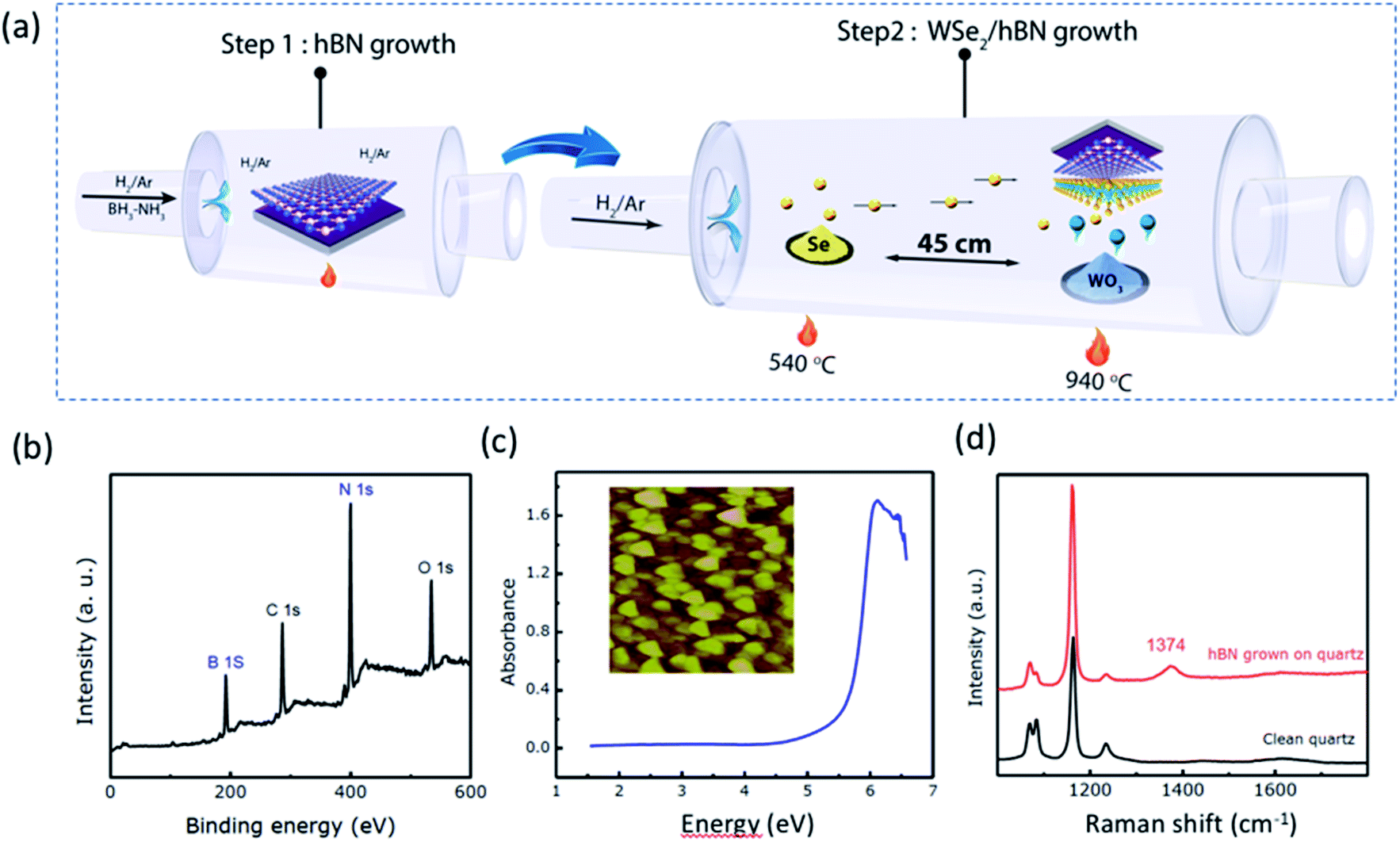 | ||
| Fig. 1 (a) A schematic view shows the CVD process of the WSe2/hBN van der Waals heterostructures using a two-step CVD method. CVD step I: hBN synthesis upon the SiO2 substrates at a high growth temperature (950 °C), the end-product of this step is illustrated; CVD step II: the growth of the WSe2 film on the hBN film, the growth conditions and the end-product are schemed. Characterization of hBN film grown on Si/SiO2 with the growth time of 1 h. (b) XPS survey. Characterization of hBN film grown on a quartz substrate with the growth time of 1 h. (c) The UV-visible absorption spectrum of hBN grown on the quartz substrate, measured at room temperature. Inset shows the AFM image of the sample. The image size is 1 μm. The root mean squared roughness Rq was calculated to be 8 nm. (d) Raman spectra of a clean quartz substrate and hBN film grown on a quartz substrate. | ||
For the WSe2/hBN synthesis, we found that 15 min is the optimum growth time to prohibit the CVD hBN decomposition. Indeed, when we attempt to synthesize WSe2 for a long period of time (40 min) on top of the CVD-hBN film, we found that the hBN film had completely decomposed. To show clearly the hBN effect as the substrate on the WSe2 growth, we proceed to WSe2 growth on SiO2 and quartz substrates, under the same growth condition. Fig. 2a exhibits the optical images of WSe2 grown on the hBN at 950 °C with a flowing rate of H2 (20 sccm). The growth under this condition yielded to multilayered WSe2 films, which is confirmed by the optical microscopy images as WSe2 domains (yellow triangles) on top of WSe2 film (dark-green areas) and Raman spectroscopy. Based on our observation, the triangular domains on top of the WSe2 layer, which have domain sizes in the range of 10 to 20 μm, could merge to form a continuous WSe2 film. A high growth temperature tends to favor the multilayer growth of WSe2. However, the WSe2 crystal synthesis on top of SiO2 exhibited smaller domains with an average domain size around 15 μm, which can be referred to the rough surface or the charge impurities of the SiO2 substrate. Based on the above results, under an optimized experimental condition (950 °C and 15 sccm of H2) a high continuous WSe2 layer could be obtained on top of hBN/SiO2 (Fig. 2c and d). Due to the elimination of the substrate defects such as charged impurities and substrate roughness, WSe2 crystals growth on the h-BN layer leads to a large film size above 400 micrometer, which is larger than the WSe2 crystals grown on SiO2 and quartz substrates (Fig. 2b). Homogeneity in color contrast on the optical image obviously indicates that the large-area monolayer WSe2 appeared with a flat and uniform surface. The growth of WSe2 on the hBN film is also larger than other TMDC crystals such as WSe2, WS2, and MoSe2 grown on top of SiO2 substrates.33–36 Eventually, by relatively decreasing both growth temperature and H2 gas flow rate (15 sccm), the layer number of WSe2 is decreased, and WSe2 triangular domains are not observed suggesting a homogeneous WSe2 layer (Fig. 2c). Fig. S1† shows optical images of hBN on SiO2/Si and quartz substrates, clearly showing continuous hBN layers (cm scale). The SEM and energy dispersive X-ray (EDX) elemental mapping are shown in Fig. S1c and d.† In addition, TEM and SAED, was performed on the edge of suspended pristine hBN layers by using a partial etch of the substrate.37 A bright-field TEM image illustrated in Fig. S2a† reveals a continuous and transparent layer and the SAED measurement shown in the Fig. S2b† gives the expected hexagonal lattice structure of hBN monolayer. The data shown in Fig. S1 and S2† confirm continuous hBN layer growth on SiO2/Si substrates.
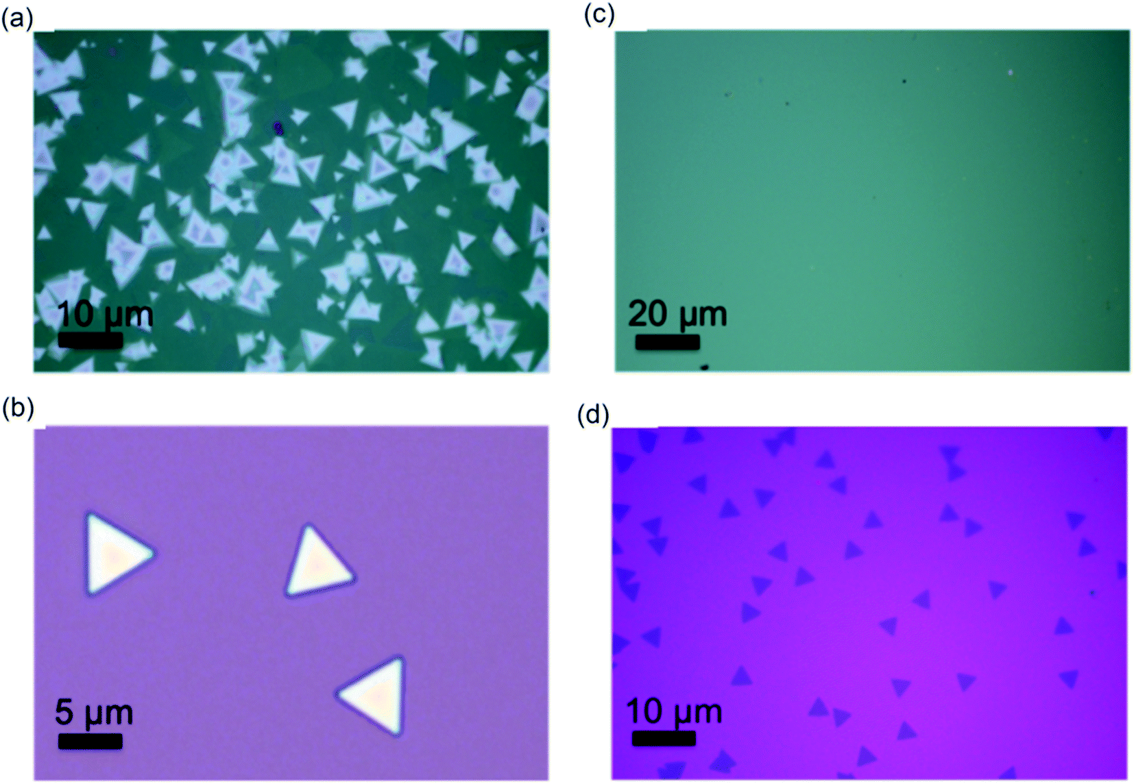 | ||
| Fig. 2 (a and b) Show the optical microscopy (OM) images of the multilayered WSe2 on the hBN film and the SiO2 substrate, respectively, at the same growth condition. (c and d) Shows the OM images of the monolayer WSe2/hBN and WSe2/SiO2, respectively. | ||
The growth mechanism could be explained by a simple dissociation, adsorption, and diffusion process in which the W and S adsorb on top of hBN and assemble into WSe2 film. Indeed, the hBN growth on top of SiO2 leads to a smoother surface. Fig. 3 illustrates the AFM images and Raman spectra of as-grown hBN films on Si/SiO2 substrates with different carrier gas flow rates. The thickness of each film was estimated using spectroscopic ellipsometry. A single Stokes peak located at 1374 cm−1 corresponding to the E2g vibration mode of hBN is observed (Fig. 3a and b). The smaller peak at 1450 cm−1 is assigned as the third order Si transverse optical (TO) phonon which is due to the underlying Si/SiO2 substrate.38 We have found that the hBN film is smoother and thinner as the carrier gas flow rate increases. We have observed different Raman shift for our hBN film in the range of 1370–1375 cm−1. The shifting of hBN Raman peak has been observed in literature. It was found that the Raman peak frequency would shift to a higher frequency under a compressive stress.39 It was reported that monolayer hBN exhibits a blue shifted Raman peak in comparison to its position in bulk hBN.40 Interestingly, Pakdel et al. found that the high-frequency E2g phonon mode in hBN shifted to a higher frequency and broadened as the crystallite size decreased.41 They established relationships between the hBN frequency shift, the broadening of the mode, and the crystallite size. The hBN peak is slightly shifted to a higher frequency as the carrier gas flow rate increased (Fig. 3c). This may suggest that the crystalline size of hBN shrank. Using 15 sccm carrier gases, we have estimated a crystallite size of ∼4 nm based on the reported dependence of Raman shift and crystallite size, however, the AFM measurements give the crystallite size average of ∼18 nm. We have observed a decrease in hBN film thickness as the carrier gas flow rate increased. Moreover, as the film grew thicker, it roughened due to surface irregularities and multiple grain boundaries. Thus, as the first step, we succeeded in growing hBN on Si/SiO2 and quartz substrates using CVD without the aid of any metal catalyst and the grown hBN film is thinner and smoother. Moreover, the carrier gas flow rate affects the CVD grown hBN film roughness and thickness. Large area hBN films with the thickness of 2 nm and rms roughness of 0.6 nm, as made evident by the slightly changed green color of the Si/SiO2 substrate (Fig. 2c).
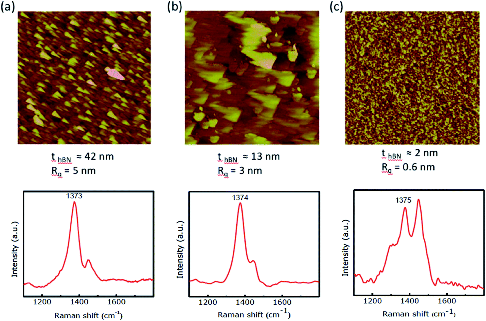 | ||
| Fig. 3 Characterization of hBN film grown on Si/SiO2 with the growth time of 1 h and variable carriers gas flow rates. AFM image and Raman spectrum of hBN film grown on Si/SiO2 substrate in 5 sccm of H2 and 5 sccm of Ar (a), 10 sccm of H2 and 10 sccm of Ar (b), 15 sccm of H2 and 15 sccm of Ar (c). The image size is 1 μm. The root mean squared roughness Rq was calculated using a Nanoscope analyzer. The thickness of the hBN film was estimated using spectroscopic ellipsometry. | ||
Raman and PL were performed in order to investigate the crystal structure and the band gap of the resulting WSe2/hBN film heterostructure.42,43 Fig. 4a shows Raman peak frequency E2g mode of the underneath hBN layer, which located at 1373 cm−1. This is consistent with the CVD grown hBN binding energy previously reported.21,28 This peak evidently confirmed the presence of the underlying hBN after completing the second CVD growth process step of the WSe2 materials. The Raman spectra of the WSe2 film showed two modes E12g and A1g at 249 cm−1 and 251 cm−1, respectively. The layer number of WSe2 can be measured by the difference between these intensity peaks. Fig. 4b demonstrates the typical Raman spectra taken from a multilayer CVD grown WSe2 on the hBN layer at 950 °C/20 sccm H2. The Raman spectra of the monolayer WSe2 is shown in Fig. 4c grown at (950 °C/15 sccm H2). The sharp peak refers to the mode E12g at 249 cm−1 and the absence of the peak at around 307 cm−1 (A21g vibration mode) confirms that the synthesized heterostructure in these growth parameters was a monolayered WSe2. The as-synthesized WSe2/hBN heterostructures at different growth conditions were characterized using Raman mapping. Raman intensity mapping recorded over a 20 μm2 area for the underlying hBN film (Fig. 4f and g). These also reveal that the uniform color contrast over the whole area clearly shows a continuous and homogeneous hBN film on top of the SiO2 substrate. A Raman map of hBN E12g (∼1369 cm−1) peak intensity is shown in Fig. S3 (see ESI†). It is clear from this image that the intensity is very uniform indicating a uniform thickness. The Raman mapping of the as-synthesized multilayer WSe2 films is also shown in Fig. 4h. The red regions on the Raman mapping correspond to the multilayer WSe2 while the yellow regions correspond to the multilayer continuous film WSe2 domains, which grew overlapping. The Raman intensity map of the peaks (249 and 307 cm−1) further demonstrates the synthesis of the uniform WSe2 monolayer on top of the hBN film at (940 °C/15 sccm H2) as is indicated in Fig. 4i. The Raman map demonstrates the same color throughout the entire monolayer, indicating a highly homogeneous crystal quality. In addition to Raman spectroscopy, the as-synthesized WSe2/hBN heterostructure was further examined using X-ray photoelectron spectroscopy as shown in Fig. S1.† Fig. S1a† represents the B 1s peaks at binding energy ∼190.2 eV for the B–N bond. Fig. S1b† shows the N 1s peak at binding energy ∼397.6 eV for the N–B bonding. These peaks are consistent with those previously reported for monolayer hBN.44–46 Both B 1s and N 1s confirm that the hBN film still exists after the WSe2 growth is completed in the second CVD step. The XPS spectra of the top layer CVD grown WSe2 is present in Fig. S4c and d,† respectively. The binding energies at 32.8, 36.8, 39.4 eV are assigned to the W 4f7/2, W 4f5/2 and W 5p3/2, respectively. The presence of the two binding peaks at 55.8 and 56.7 eV are assigned to the Se3 d3/2, and Se3 d5/2, respectively. These resulting values are consistent with previously published values.47–49
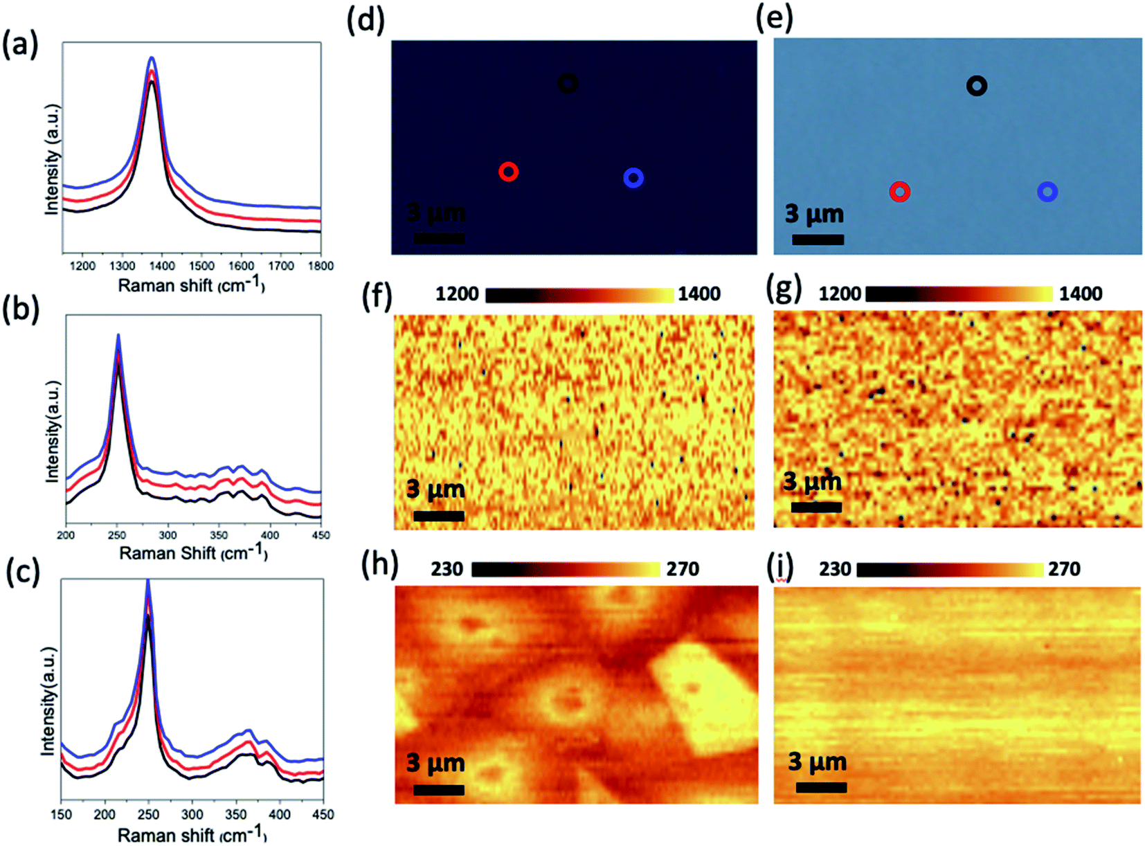 | ||
| Fig. 4 Raman investigation of the WSe2/hBN heterostructure. (a) Displays three Raman spectra of the underlying hBN film collected from different positions of the sample. (b) Shows the Raman spectrum of the multilayer WSe2 grown at (950 °C/20 sccm H2). (c) Displays the Raman spectrum of the monolayer WSe2 synthesized at (940 °C/15 sccm H2). (d and e) Are optical images of the WSe2/hBN synthesized (950 °C/20 sccm H2) and (950 °C/15 sccm H2), respectively. (f and g) Are Raman mapping images of the underlying hBN materials taken from the regions of panels (d) and (e) following the Stokes E12g (∼1369 cm−1) peak intensity of hBN integrated between 1300 and 1400 cm−1. (h and i) Show the Raman map of the E12g (∼249 cm−1) peak intensity of the WSe2 taken from the regions of panels (d) and (e), respectively. | ||
The optical property of the monolayer WSe2/hBN heterostructure film grown at (950 °C to 15 sccm H2) was further characterized using photoluminescence (PL) as shown in Fig. 5. The WSe2 films exhibited strong PL spectra localized at approximately 760 nm with a narrow FWHM (80 meV), in comparison with PL intensity spectra of the WSe2 on the SiO2 and the quartz substrate as seen in Fig. 5b and c, respectively. Ordinarily, the quality of the materials and the lifetime of electron–hole coupling are related to the FWHM of the PL emission peak.12,50 The narrow FWHM of WSe2/hBN can be a result of the high crystallinity, clean interfaces and reduced charged impurities of the continuous films when grown on hBN. The PL mapping of the synthesized WSe2 materials on different substrates, such as hBN, SiO2, and quartz is shown in Fig. 5d–f, respectively. The difference in the PL mapping colors does not reflect the emission color. We can clearly conclude that the underlying insulating hBN is an ideal substrate for reducing structural defects, improving optical properties, and promising for growth scalability.
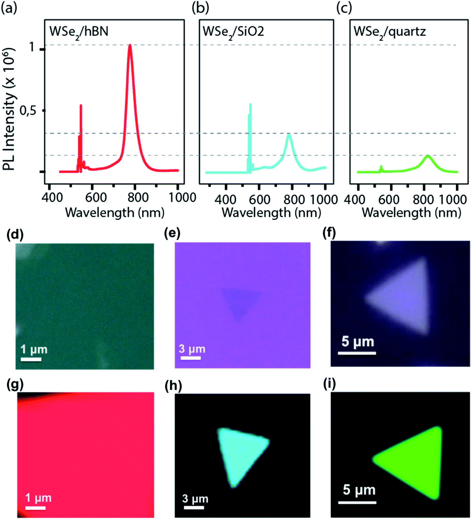 | ||
| Fig. 5 PL investigation of the growth of WSe2 on various substrates. (a–c) Display the monolayer PL spectra of the WSe2/hBN, WSe2/SiO2 and WSe2/quartz, respectively. (d–f) Demonstrate optical images of the WSe2/hBN, WSe2/SiO2 and WSe2/quartz, respectively. (g–i) Show PL intensity mapping of the monolayer WSe2/hBN, WSe2/SiO2 and WSe2/quartz, respectively. | ||
Conclusions
We have accomplished the synthesis of a large area, uniform, and high quality two-dimensional atomic layer WSe2 directly on hBN substrates using a two-step CVD approach without the need for the transfer process. It is concluded that the surface morphology of the substrate influences the WSe2 growth materials. By using an hBN film as an insulating substrate, a large area (400 μm2) WSe2/hBN heterostructure was synthesized, which was much larger than those obtained using a SiO2 substrate. To obtain an atomically smooth surface WSe2/hBN van der Waals heterostructure, the growing time, temperature, and the amount of H2 were optimized for WSe2 material growth. The growth time was optimized to be 15 min at high temperature 950 °C and high concentration of H2, 15 sccm. The growth mechanism could be explained by a simple dissociation, adsorption, and diffusion process in which the W and S adsorb on top of hBN and assemble into WSe2 film. The properties and the nanostructure of the van der Waals layers were confirmed using different techniques including optical microscopy, Raman, PL, and XPS. Raman and photoluminescence mapping showed that the as-synthesized heterostructure expresses optical modulation. The narrow FWHM of the emission peak (80 meV) of the WSe2/hBN indicates the high crystallinity and the quality of this heterostructure. This work indicates that our two-step growth process can be used as a common approach to synthesize other wafer-scale and contamination-free out of plane heterostructure 2D materials.Conflicts of interest
There are no conflicts to declare.Acknowledgements
This work was supported through funding from the Natural Science and Engineering Research Council of Canada (NSERC), the Canada Research Chairs program (CRC) and Canada Foundation for Innovation. We acknowledge NanoQAM center for the characterization facilities. Also, a special thanks goes to the Taibah University, Kingdom of Saudi Arabia for Alahmadi's Fellowship.References
- R. F. Frindt and A. D. Yoffe, Proc. R. Soc. London, Ser. A, 1963, 273, 69–83 Search PubMed.
- K. Wang, B. Huang, M. Tian, F. Ceballos, M.-W. Lin, M. Mahjouri-Samani, A. Boulesbaa, A. A. Puretzky, C. M. Rouleau and M. Yoon, ACS Nano, 2016, 10, 6612–6622 CrossRef CAS PubMed.
- J. C. Shaw, H. Zhou, Y. Chen, N. O. Weiss, Y. Liu, Y. Huang and X. Duan, Nano Res., 2014, 7, 1–511 CrossRef.
- Z. Li, S. Yang, R. Dhall, E. Kosmowska, H. Shi, I. Chatzakis and S. B. Cronin, ACS Nano, 2016, 10, 6836–6842 CrossRef CAS PubMed.
- Z. Li, G. Ezhilarasu, I. Chatzakis, R. Dhall, C.-C. Chen and S. B. Cronin, Nano Lett., 2015, 15, 3977–3982 CrossRef CAS PubMed.
- K. Xu, Z. Wang, X. Du, M. Safdar, C. Jiang and J. He, Nanotechnology, 2013, 24, 465705 CrossRef PubMed.
- S. M. Eichfeld, L. Hossain, Y. Lin, A. F. Piasecki, B. Kupp, a G. Birdwell, R. a. Burke, N. Lu, X. Peng, J. Li, A. Azcatl, S. Mcdonnell, R. M. Wallace, M. J. Kim, T. S. Mayer, J. M. Redwing and J. a Robinson, ACS Nano, 2015, 9, 2080–2087 CrossRef CAS PubMed.
- G. Clark, S. Wu, P. Rivera, J. Finney, P. Nguyen, D. H. Cobden and X. Xu, APL Mater., 2014, 101101, 1–6 Search PubMed.
- H.-J. Chuang, X. Tan, N. J. Ghimire, M. M. Perera, B. Chamlagain, M. M.-C. Cheng, J. Yan, D. Mandrus, D. Tománek and Z. Zhou, Nano Lett., 2014, 14, 3594–3601 CrossRef CAS PubMed.
- Q. H. Wang, K. Kalantar-Zadeh, A. Kis, J. N. Coleman and M. S. Strano, Nat. Nanotechnol., 2012, 7, 699 CrossRef CAS PubMed.
- J. S. Ross, P. Klement, A. M. Jones, N. J. Ghimire, J. Yan, D. G. Mandrus, T. Taniguchi, K. Watanabe, K. Kitamura and W. Yao, Nat. Nanotechnol., 2014, 9, 268 CrossRef CAS PubMed.
- M. Okada, T. Sawazaki, K. Watanabe, T. Taniguch, H. Hibino, H. Shinohara and R. Kitaura, ACS Nano, 2014, 8, 8273–8277 CrossRef CAS PubMed.
- H. Wang, T. Taychatanapat, A. Hsu, K. Watanabe, T. Taniguchi, P. Jarillo-herrero and T. Palacios, Nano, 2011, 32, 1209–1211 CAS.
- S. Bertolazzi, D. Krasnozhon and A. Kis, ACS Nano, 2013, 7, 3246–3252 CrossRef CAS PubMed.
- H. Lim, S. I. Yoon, G. Kim, A.-R. Jang and H. S. Shin, Chem. Mater., 2014, 26, 4891–4903 CrossRef CAS.
- K. I. Bolotin, K. J. Sikes, Z. Jiang, M. Klima, G. Fudenberg, J. Hone, P. Kim and H. L. Stormer, Solid State Commun., 2008, 146, 351–355 CrossRef CAS.
- J.-H. Chen, C. Jang, S. Xiao, M. Ishigami and M. S. Fuhrer, Nat. Nanotechnol., 2008, 3, 206 CrossRef CAS PubMed.
- W. Bao, X. Cai, D. Kim, K. Sridhara and M. S. Fuhrer, Appl. Phys. Lett., 2013, 102, 042104 CrossRef.
- C. R. Dean, a. F. Young, I. Meric, C. Lee, L. Wang, S. Sorgenfrei, K. Watanabe, T. Taniguchi, P. Kim, K. L. Shepard and J. Hone, Nat. Nanotechnol., 2010, 5, 722–726 CrossRef CAS PubMed.
- N. Jain, T. Bansal, C. a. Durcan, Y. Xu and B. Yu, Carbon, 2013, 54, 396–402 CrossRef CAS.
- S. Behura, P. Nguyen, S. Che, R. Debbarma and V. Berry, J. Am. Chem. Soc., 2015, 137, 13060–13065 CrossRef CAS PubMed.
- I. Meric, C. R. Dean, N. Petrone, L. Wang, J. Hone, P. Kim and K. L. Shepard, Proc. IEEE, 2013, 101, 1609–1619 CAS.
- G. Lu, T. Wu, Q. Yuan, H. Wang, H. Wang, F. Ding, X. Xie and M. Jiang, Nat. Commun., 2015, 6, 6160 CrossRef CAS PubMed.
- J. Bao, K. Jeppson, M. Edwards, Y. Fu, L. Ye, X. Lu and J. Liu, Electron. Mater. Lett., 2016, 12, 1–16 CrossRef CAS.
- S. Wang, X. Wang and J. H. Warner, ACS Nano, 2015, 9, 5246–5254 CrossRef CAS PubMed.
- Y. Gong, J. Lin, X. Wang, G. Shi, S. Lei, Z. Lin, X. Zou, G. Ye, R. Vajtai, B. I. Yakobson, H. Terrones, M. Terrones, B. K. Tay, J. Lou, S. T. Pantelides, Z. Liu, W. Zhou and P. M. Ajayan, Nat. Mater., 2014, 13, 1135–1142 CrossRef CAS PubMed.
- Y. Feng, K. Zhang, F. Wang, Z. Liu, M. Fang, R. Cao, Y. Miao, Z. Yang, W. Mi, Y. Han, Z. Song and H. S. P. Wong, ACS Appl. Mater. Interfaces, 2015, 7, 22587–22593 CrossRef CAS PubMed.
- S. Wang, X. Wang and J. H. Warner, ACS Nano, 2015, 9, 5246–5254 CrossRef CAS PubMed.
- D. Liu, X.-Q. Yan, H.-W. Guo, Z.-B. Liu, W.-Y. Zhou and J.-G. Tian, J. Appl. Phys., 2020, 128, 43101 CrossRef CAS.
- B. Liu, M. Fathi, L. Chen, A. Abbas, Y. Ma and C. Zhou, ACS Nano, 2015, 9, 6119–6127 CrossRef CAS PubMed.
- M. Merisalu, T. Kahro, J. Kozlova, A. Niilisk, A. Nikolajev, M. Marandi, A. Floren, H. Alles and V. Sammelselg, Synth. Met., 2015, 200, 16–23 CrossRef CAS.
- B. V. A. Rao, M. Y. Iqbal and B. Sreedhar, Corros. Sci., 2009, 51, 1441–1452 CrossRef.
- C. Jung, S. M. Kim, H. Moon, G. Han, J. Kwon, Y. K. Hong, I. Omkaram, Y. Yoon, S. Kim and J. Park, Sci. Rep., 2015, 5, 15313 CrossRef CAS PubMed.
- Y. Rong, Y. Fan, A. L. Koh, A. W. Robertson, K. He, S. Wang, H. Tan, R. Sinclair and J. H. Warner, Nanoscale, 2014, 6, 12096–12103 RSC.
- X. Ma, R. Zhang, C. An, S. Wu, X. Hu and J. Liu, Chin. Phys. B, 2019, 28, 37803 CrossRef CAS.
- J. Li and M. Östling, Electronics, 2015, 4, 1033–1061 CrossRef CAS.
- W. D. McFall, D. R. McKenzie and R. P. Netterfield, Surf. Coat. Technol., 1996, 81, 72–78 CrossRef CAS.
- F. Mahvash, S. Eissa, T. Bordjiba, A. C. Tavares, T. Szkopek and M. Siaj, Sci. Rep., 2017, 7, 42139 CrossRef CAS PubMed.
- S. Reich, A. C. Ferrari, R. Arenal, A. Loiseau, I. Bello and J. Robertson, Phys. Rev. B: Condens. Matter Mater. Phys., 2005, 71, 205201 CrossRef.
- T. Taira, S. Obata and K. Saiki, Appl. Phys. Express, 2017, 10, 55502 CrossRef.
- A. Pakdel, C. Zhi, Y. Bando, T. Nakayama and D. Golberg, ACS Nano, 2011, 5, 6507–6515 CrossRef CAS PubMed.
- S. Das, M. Kim, J. Lee and W. Choi, Crit. Rev. Solid State Mater. Sci., 2014, 39, 231–252 CrossRef CAS.
- S.-Y. Chen, C. Zheng, M. S. Fuhrer and J. Yan, Nano Lett., 2015, 15, 2526–2532 CrossRef CAS PubMed.
- D. Lee and S. H. Song, RSC Adv., 2017, 7, 7831–7835 RSC.
- G. R. Bhimanapati, D. Kozuch and J. A. Robinson, Nanoscale, 2014, 6, 11671–11675 RSC.
- F. Mahvash, E. Paradis, D. Drouin, T. Szkopek and M. Siaj, Nano Lett., 2015, 15, 2263–2268 CrossRef CAS PubMed.
- J. K. Huang, J. Pu, C. L. Hsu, M. H. Chiu, Z. Y. Juang, Y. H. Chang, W. H. Chang, Y. Iwasa, T. Takenobu and L. J. Li, ACS Nano, 2014, 8, 923–930 CrossRef CAS PubMed.
- J. Huang, L. Yang, D. Liu, J. Chen, Q. Fu, Y. Xiong, F. Lin and B. Xiang, Nanoscale, 2015, 7, 4193–4198 RSC.
- B. Nie, T. Chen, M. Liang, Y. Wang, J. Zhong, Y. Zhu and E. Mollwo, J. Appl. Polym. Sci., 2011, 30, 9 Search PubMed.
- Z. Yao, J. Liu, K. Xu, E. K. C. Chow and W. Zhu, Sci. Rep., 2018, 8, 5221 CrossRef PubMed.
Footnote |
| † Electronic supplementary information (ESI) available. See DOI: 10.1039/d1ra02523f |
| This journal is © The Royal Society of Chemistry 2021 |