DOI:
10.1039/D1RA02368C
(Paper)
RSC Adv., 2021,
11, 16015-16025
In situ laser irradiation: the kinetics of the changes in the nonlinear/linear optical parameters of As50Se40Sb10 thin films for photonic applications
Received
25th March 2021
, Accepted 25th April 2021
First published on 30th April 2021
Abstract
The photosensitivity of amorphous chalcogenide thin films brings out light-induced changes in the nonlinear and linear optical parameters upon sub-bandgap and bandgap laser irradiation. The present work reports the in situ laser irradiated changes in the optical properties of As50Se40Sb10 thin films. The thermally evaporated film showed an exponential decrease in optical bandgap and increase in Urbach energy. The decay rate of the bandgap was 6.24 min and growth rate of Urbach energy was 6.67 min respectively. The dynamics of photo-induced changes were observed from the changes in linear refractive index and its dependent parameters such as 3rd order nonlinear susceptibility, nonlinear refractive index, dispersion and dielectric parameters. The conversion of heteropolar to homopolar bonds induced the photodarkening mechanism that changed the dispersion parameters. The decrease in Ed and Eo reduced the oscillator strength along with the zero-frequency dielectric constant. The optical and electrical conductivity changed significantly with time. The changes were saturated with time which brings stability in the film properties that is useful for various optical applications. However, no structural and compositional changes upon laser irradiation were noticed from the X-ray diffraction and EDX studies respectively. The surface homogeneity was checked from the FESEM picture.
1. Introduction
The unique electronic structure of the chalcogenide materials makes them favourable for light-induced changes due to the photo excited carriers in the form of localized defect states in the gap region.1 Photo-induced changes by means of a laser irradiation process is one of the simple and environment-friendly methods that enable precise structure and optical changes in a controlled manner with minimal surface damage.2,3 It leads to bond breaking and rearrangements resulting in modifications of localized structures of the amorphous material that ultimately brings out the changes in physical and optical properties such as transmittance, absorption and extinction coefficient, refractive index and optical bandgap, etc.4–6 The change in bandgap values mainly leads to two important phenomena, photodarkening (PD)7 (decrease in bandgap) and photobleaching (PB)8 (increase in bandgap). The PD is most often observed in arsenic-based films9 whereas PB is common in Ge-based chalcogenide films caused by the intrinsic structural changes.10 However, there also exist both PD and PB simultaneously in some materials.11 The transient and metastable photoinduced changes are well distinguished by the change in pulse width of the laser beam and duration of laser pulse.12 Similarly, the time evolution of the laser irradiation also significantly affects the kinetics of the changes in the film which are measured by the spectroscopic techniques.13 The majority of the laser irradiation spectroscopic studies on films are using ex situ measurements in which the data were recorded before and after the laser illumination. This gives only the metastable and permanent optical changes.14,15 But the dynamics of the changes with laser illumination (i.e., during the illumination time) are not clear by ex situ measurement. The advantage of the in situ study lies in its systematic observation of kinetic changes with time during illumination.16 The in situ method is of two types: the first one in which the single light source acts as both pump and probe beam whereas, in the second kind, the pump beam is the exciting laser light with energy very close to the optical bandgap of the studied material and the probe beam is usually a low intensity monochromatic white light source that coincides with the pump beam to characterize the illuminated portion.17 The various researchers have investigated the change in optical bandgap and refractive index either by ex situ or in situ measurements.16,18,19 The kinetics of the associated nonlinear changes is not clear for the laser-irradiated process.
The choice of As–Se–Sb thin films lies on their application for optical switching and memory devices.20,21 The photoconductivity study in As30Se70−xSbx and AsxSb15Se85−x films provided detailed information regarding the free carrier transport and photo generation of the carriers.22,23 The thermal and electrical parameters of Se65−xAs35Sbx films were calculated from the resistivity-temperature dependence studies.24 Pradhan et al. have studied the in situ kinetics of the linear optical changes in As40Se53Sb07 films5 and the ex situ 3rd order nonlinearity change.25 Though ex situ linear and nonlinear optical properties have been studied to some extent,26,27 the in situ nonlinear/linear dynamic response of the As–Se–Sb materials upon laser irradiation is very rare. We have employed the in situ pump-probe method to observe and correlate the linear and non-linear optical constants with laser irradiation time which brings out the detailed kinetics of such changes for various optical applications. The present study was done on thermally evaporated As50Se40Sb10 thin films of ∼800 nm. We have estimated the exponential decay rate of optical bandgap with in situ laser irradiation at different time period and the gradual decrease in the nonlinear parameters in the films.
2. Experimental procedure
The bulk As50Se40Sb10 sample was prepared by conventional melt quenching method from high purity elements with proper stoichiometric calculation. The sealed quartz ampoule containing the elements was gradually heated to ∼10![[thin space (1/6-em)]](https://www.rsc.org/images/entities/char_2009.gif) 00 °C for 24 h inside the furnace. After the complete homogenization of the melt, the ampoule was taken out from the furnace and quenched rapidly in ice-cold water to get the bulk sample. The quenched quartz ampoule was then broken and the obtained bulk samples were ground to powder form. The powdered form of bulk sample was used to prepare the thin film (∼800 nm thickness) in the vacuum coating unit (HIND-HIVAC Model 12A4D) under 10−5 Torr. The powdered sample was placed on the molybdenum boat inside the coating unit. The boat was heated slowly till the material was evaporated and deposited in form of a thin film on the pre-clean glass substrate. The substrate holder was continuously rotated to obtain a uniform and homogenous thin film. The rate of deposition was kept at 0.5 nm s−1 and the crystal thickness monitor attached to the coating unit was used to measure the thickness of the film.
00 °C for 24 h inside the furnace. After the complete homogenization of the melt, the ampoule was taken out from the furnace and quenched rapidly in ice-cold water to get the bulk sample. The quenched quartz ampoule was then broken and the obtained bulk samples were ground to powder form. The powdered form of bulk sample was used to prepare the thin film (∼800 nm thickness) in the vacuum coating unit (HIND-HIVAC Model 12A4D) under 10−5 Torr. The powdered sample was placed on the molybdenum boat inside the coating unit. The boat was heated slowly till the material was evaporated and deposited in form of a thin film on the pre-clean glass substrate. The substrate holder was continuously rotated to obtain a uniform and homogenous thin film. The rate of deposition was kept at 0.5 nm s−1 and the crystal thickness monitor attached to the coating unit was used to measure the thickness of the film.
The in situ laser irradiation of the thin film was done inside the spectrometer (Bruker IFS 66v/S) as presented in ref. 19. The pump beam was a diode-pumped solid-state laser (DPSS) of wavelength 532 nm with an intensity of 4 mW cm−2 and the probing was done through a white light source with wavelength ranging from 400–1200 nm. The pump beam was expanded by using a beam expander to enclose a larger area than the probe beam with a complete overlapping of laser spot over the probe light spot from the spectrometer. The data were recorded continuously as a function of time up to saturation of the observed changes. Such small intensity laser beam with a large beam spot on the sample resulted in a negligible rise in temperature ∼6 K as calculated by following the procedure outlined in ref. 28 infers the photoelectronic change by laser irradiation and not due to thermal effect.
The structural study of the as-prepared and laser-irradiated film was done by X-ray diffractometer (Bruker D8 Advance) with Cu-Kα radiation (λ = 1.54 Å). The data scan was done at 1° min−1 scan speed, 0.02° step-up value in 2θ range of 10°–80° at a grazing angle of 1°. The surface morphological and elemental analysis was performed by the FESEM (JEOL) and EDS (facility attached to the FESEM unit) respectively. The surface scan was done at 3–4 positions within 1 cm2 sample size at a pressure of 2 × 10⁻⁷ Torr.
3. Results and discussion
3.1 Linear optical parameters
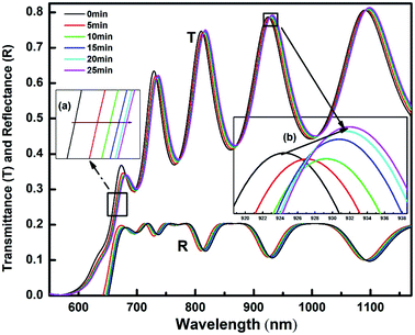
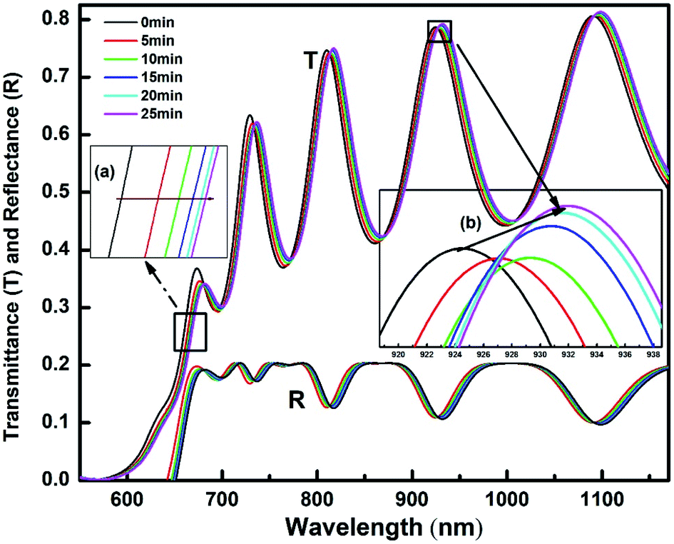
3.1.1 Transmittance (T) and reflectance (R). Fig. 1 presents the transmittance (T) and reflectance (R) spectra of the laser-irradiated film at different time frames during the in situ measurement. The absorption edge gradually shifted towards the higher wavelength regime upon irradiation with time and saturated slowly (Fig. 1a inset). This clearly infers the change in the band structure of the film causing a decrease in the optical bandgap. The appearance of the interference fringe at a higher wavelength (above 700 nm) in the non-irradiated film (0 min) presents the uniformity and homogeneity of the film29 which changed the position with laser irradiation (Fig. 1b inset). The shift in the fringe is small (∼9 nm shift between 0 min and 25 min laser irradiated film). The re-distribution of energy due to the interference causes maxima and minima in a spectrum of transmitted regions. This is due to the impact of the dynamic response of the films presenting the changes in fringe strength (TM–Tm) due to laser irradiation.17 The transmittance value increased slightly (∼1%) with laser irradiation bringing more transparency at the higher wavelength side. A similar behaviour but in an opposite manner can be observed in R spectra. The overall behaviour of these spectra suggests that the As50Se40Sb10 thin films are becoming more transparent during the laser irradiation.
 |
| | Fig. 1 T and R spectra of the films at different irradiation time. | |
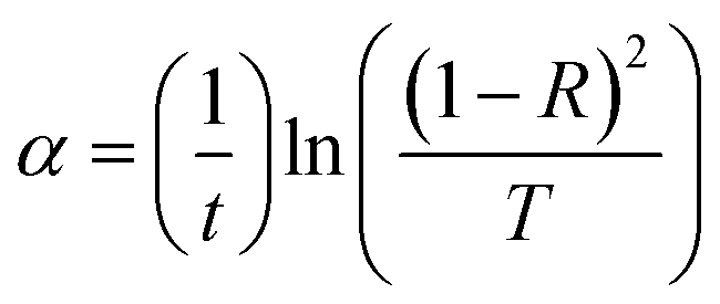
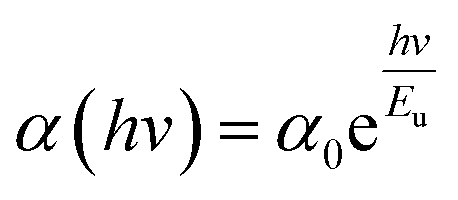
3.1.2 Absorption coefficient, extinction coefficient, optical bandgap and Urbach energy. The absorption coefficient (α) is an important parameter that gives information regarding the type of band structure and optical bandgap of the films. It signifies the ability of the films for absorbing light. The value of α was calculated by using the relation30| |
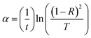 | (1) |
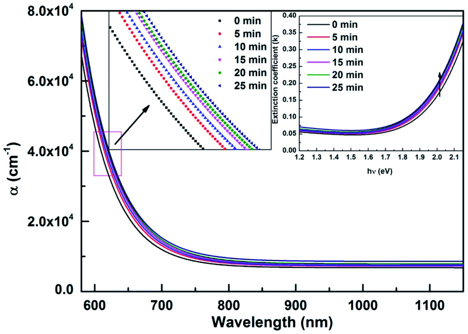
where ‘t’ represents the thickness of the films, T and R being the transmittance and reflectance value. Fig. 2 shows the changes in ‘α’ values with irradiation time represents the behaviour of the absorption coefficient with the irradiation time which all saturates at the higher wavelength regime. The increase in ‘α’ values with irradiation time (Fig. 2 inset) suggests the increase in the localized states in the gap which causes a decrease in the bandgap values and surface modifications of the films.31 The shifting of absorption edge towards higher wavelength with the increase in irradiation time confirms the reduction in bandgap and the bandgap change saturates with time.
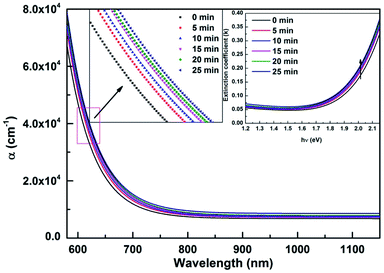 |
| | Fig. 2 The variation of ‘α’ and ‘k’ (inset) with irradiation time. | |
The extinction coefficient (k) which is also known as the absorption index provides information regarding a reasonable interaction between the material and the electric field of the electromagnetic radiation and describes the decay in oscillation amplitude of the electric field.32 The measurement of the fraction of light lost due to absorption while propagating through the material was evaluated by using the relation
The value of ‘k’ was found to be increased with irradiation time and saturates as seen from Fig. 2 (inset). A significant shift towards a higher wavelength suggests a slight increase in materials optical loss with laser irradiation time interval. This parameter is essential for designing suitable photonic devices.
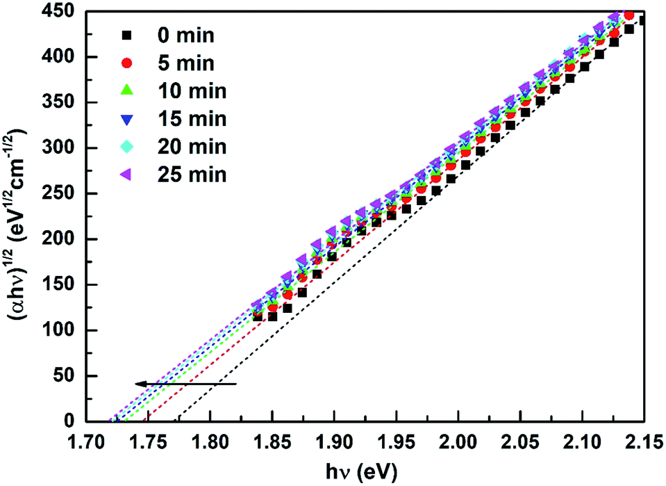
Among the three absorption regions of the amorphous materials, the region α ≥ 104 cm−1 which is known as the high absorption region determines the nature of optical transition in the film by the Tauc relation33
where
B is the Tauc parameter,
hv is photon energy and ‘
p’ is an exponent which represents the nature of the electronic transition such as direct allowed (
p = 1/2), indirect allowed (
p = 2), direct forbidden
p = 1/3 and indirect forbidden (
p = 3) respectively. The best fit to the observed data showed
p = 2 indicating the indirect allowed transition in the gap. The plot of (
αhν)
1/2 vs. hν in
Fig. 3 presents the optical band gaps (
Eg) at different irradiation time period. The reduction in
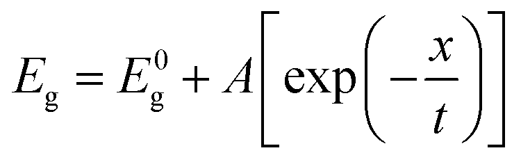
Eg with time clearly shows the PD effect which fits to the exponential decay equation
| |
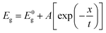 | (4) |
where
E0g is the initial optical bandgap,
x is the laser irradiation time,
A is a constant and
t is the effective time constant or the rate of darkening. The PD starts to saturate after the decay time of 6.24 min as found from the fitting of the data as shown in
Fig. 4. The change saturates after ∼20 min of irradiation. The kinetics of the changes in
Eg is well explained by the Davis–Mott model of bond breaking and rearrangement theory.
34 The incident photon energy facilitates the lone pair-lone pair interaction of the chalcogen atoms and enhanced the creation of homopolar bonds (As–As, Se–Se, Sb–Sb) from the available heteropolar bonds (As–Se, Sb–Se) through the reaction
| |
 | (5) |
 |
| | Fig. 3 Calculation of Eg for different irradiated films. | |
 |
| | Fig. 4 The fitted data of Eg and Eu with irradiation time. | |
Since the top of the valence band is formed by the lone pair electrons, the increase in lone pair-lone pair (LP–LP) interactions yields a broadening of the valence band which caused the reduction in the bandgap (PD). The photon-assisted site switching model28,35 also explains the phenomena of PD in which the incident photon energy brings a percolative growth of photon-assisted site switched chalcogenide clusters responsible for specific topological defects that reduces the optical gap. The measure of such defects in the film was evaluated from the absorption regime with 104 ≥ α ≥ 100 cm−1, which shows the exponential dependence of ‘α’ and is known as the Urbach edge.
| |
 | (6) |
where
Eu is the width of the band tail of localized states in the optical band gap and also known as the Urbach energy.
36 The slope of the linear plot between ln(
α/
α0)
vs. hν determines the value
Eu as presented in
Table 1. The fitting of
Eu also followed the exponential growth function which also inferred the rate of increase of defects time as 6.67 min nearly equal with the decay time (
Fig. 4). The increase in
Eu signifies the increase in the degree of disorder in the film that saturates after 25 min of laser irradiation resulting in PD. The creation of dangling bonds due to laser radiation increases the concentration of localized states that reduces the
Eg.
Table 1 Optical parameters of the films at different irradiation time
| Optical parameter |
0 min |
5 min |
10 min |
15 min |
20 min |
25 min |
| Optical band gap (eV) |
1.776 |
1.746 |
1.731 |
1.726 |
1.724 |
1.721 |
| Tauc parameter (B1/2) cm−1/2 eV−1/2 |
1227 |
1134 |
1105 |
1099 |
1096 |
1091 |
| Urbach energy (eV) |
0.122 |
0.130 |
0.132 |
0.134 |
0.135 |
0.136 |
| Dispersion energy (Ed) (eV) |
17.928 |
17.521 |
16.949 |
16.574 |
16.303 |
16.205 |
| Oscillator energy (Eo) (eV) |
2.74 |
2.72 |
2.69 |
2.67 |
2.65 |
2.64 |
| Static refractive index (n0) |
2.746 |
2.727 |
2.701 |
2.684 |
2.674 |
2.671 |
| Oscillator strength (E0Ed) |
49.122 |
47.657 |
45.592 |
44.252 |
43.202 |
42.781 |
| The first moments of the optical spectra (M−1) |
6.543 |
6.441 |
6.300 |
6.207 |
6.152 |
6.138 |
| The third moments of optical spectra, (M−3) |
0.8715 |
0.8705 |
0.8706 |
0.8707 |
0.8760 |
0.8806 |
| Zero frequency dielectric constant, ε∞ |
7.543 |
7.441 |
7.3 |
7.207 |
7.152 |
7.138 |
| High frequency dielectric constant, εL |
12.770 |
12.710 |
12.569 |
12.492 |
12.364 |
12.217 |
| Carrier concentration N/m* (cm3 g) |
3.904 × 1039 |
3.806 × 1039 |
3.792 × 1039 |
3.789 × 1039 |
3.743 × 1039 |
3.737 × 1039 |
| Oscillator wavelength, λo (nm) |
452 |
455 |
463 |
467 |
469 |
471 |
| Oscillator strength (s0) nm2 |
3.928 × 10⁻⁵ |
3.822 × 10⁻⁵ |
3.687 × 10⁻⁵ |
3.626 × 10⁻⁵ |
3.588 × 10⁻⁵ |
3.578 × 10⁻⁵ |
| χ1 (hν → 0) |
0.5207 |
0.5124 |
0.5012 |
0.4939 |
0.4896 |
0.4883 |
| χ3 (e.s.u.) (hν → 0) |
12.4 × 10⁻¹² |
11.7 × 10⁻¹² |
10.7 × 10⁻¹² |
10.1 × 10⁻¹² |
9.76 × 10⁻¹² |
9.66 × 10⁻¹² |
| Nonlinear refractive index (n2) (e.s.u.) |
1.70 × 10⁻¹⁰ |
1.61 × 10⁻¹⁰ |
1.49 × 10⁻¹⁰ |
1.41 × 10⁻¹⁰ |
1.37 × 10⁻¹⁰ |
1.36 × 10⁻¹⁰ |
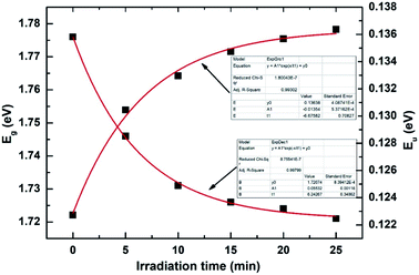
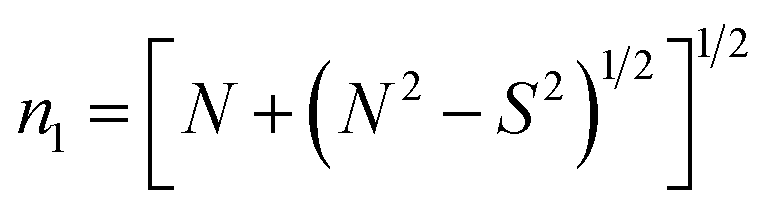
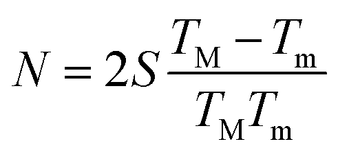
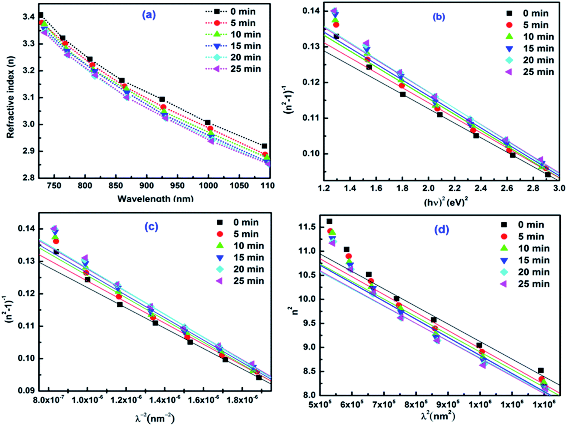
3.1.3 Linear refractive index (n). The linear refractive index (n) infers the electronic, optical and polarizability properties of a material whose variation with external stimuli is important for application point of view.37 The Swanepoel envelope method38 was used to determine the value of ‘n’ of the laser-irradiated film having uniform fringes. The approximated value of ‘n’ was calculated by the relation
where| |
 | (7) |
where TM and Tm refer to the maximum and minimum value of transmittance at a particular interference fringe of wavelength (λ) and S is the refractive index for glass substrate (1.51). The actual linear refractive index was then calculated by using 2nd = mλ where m refers to the integral or half-integral value depending on the maxima or minima. The variation of ‘n’ with wavelength at different irradiation time is shown in Fig. 5a, that depicts the gradual reduction of ‘n’ with a wavelength which is due to normal dispersion phenomena whereas the decrease of ‘n’ with irradiation time is due to the structural modifications in the localized defect states as a result of the photo-induced effect.39 This photo-induced behaviour of refractive index will be essential for various photonic applications, so it further demands detailed studies of dispersion, dielectric and nonlinear optical properties of the material.
 |
| | Fig. 5 (a) ‘n’ vs. ‘λ’ at different irradiation time (b) (n2 − 1)−1 vs. (hv)2 for the thin films (c) (n2 − 1)−1 vs. (λ)−2 for irradiated thin films (d) n2 vs. λ2 for the irradiated thin films. | |
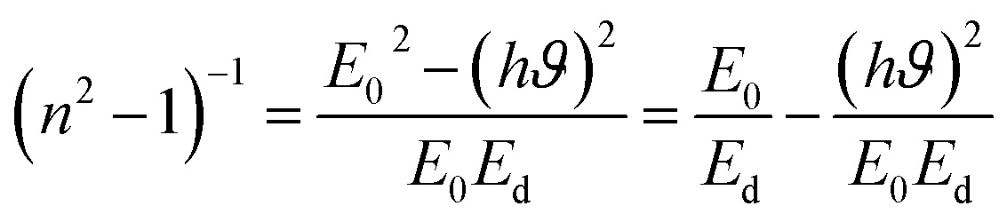
3.1.4 Dispersion parameters based on single effective oscillator model (SEO). Dispersion properties of material play an important role in deciding materials applicability in various photonic and spectral dispersion devices. The dispersion energy (Ed) and oscillator energy (Eo) were evaluated from the Wemple & Di-Domenico (WDD) single effective oscillator model40 from the relation| |
 | (8) |
The oscillator parameters were determined from slope (EoEd)−1 and intercept  values of the (n2 − 1)−1 vs. (hv)2 plot as shown in Fig. 5b. According to the WDD model, Ed can be represented by an empirical relation i.e., Ed = βNcZaNe where β is a constant, Nc is the effective coordination number of the cation, Za the formal chemical valance of the anion, Ne is the effective number of valence electrons per anion. The value of Ed represents the average strength of interband transition. The Eo represents the separation between the centres' of gravity of the valence and conduction band. Both the parameters show an overall decreasing behaviour with laser irradiation time which represents the impact on the strength of inter-band optical transition and average energy gap of the material.41 The oscillator strength of the material i.e., f = EoEd is presented in Table 1 which shows an overall decreasing behaviour. It indicates the reduction in materials oscillator strength characteristics with an increase in laser irradiation time like the change in fringe position in Fig. 1.
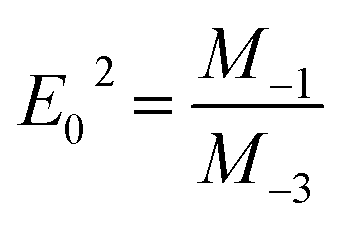
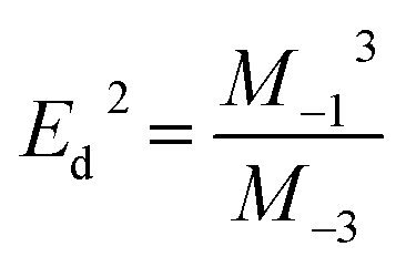
These dispersion parameters can be further utilized to estimate the first-order (M−1) and the third-order moment of optical spectra (M−3), that are related to the effective no of valence electrons in the film and can be expressed as,
, and
| |
 | (9) |
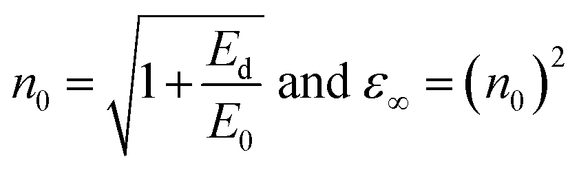
From Table 1, it can be observed that both the parameters show an overall decreasing order with an increase in irradiation time. Similarly, the zero-frequency dielectric constant (ε∞) and static refractive index n0 (when hν → 0) can be obtained by the given relation,
| |
 | (10) |
From Table 1, it can be observed that ε∞ and n0 values decreased with irradiation time like the oscillator parameters.
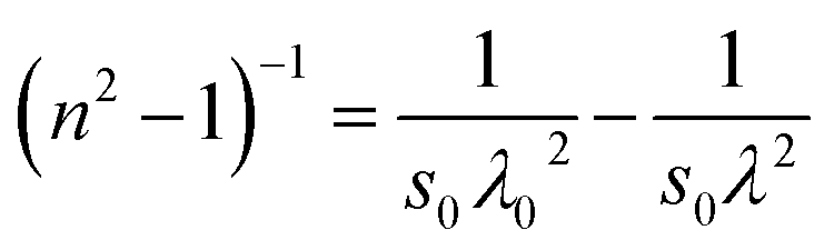
3.1.5 Dispersion parameters based on Sellmeier's classical dispersion model. Based on Sellmeier's classical dispersion model, the relationship between the refractive index at a lower frequency can be expressed by the given relation,42| |
 | (11) |
where s0 and λ0 are known as the strength of oscillator and oscillator wavelength respectively. These parameters were obtained from the vertical intercept and slope of the (n2 − 1)−1 vs. (λ)−2 the plot presented in Fig. 5c. From Table 1, the s0 values decreased whereas the λ0 values were increased by the impact of laser irradiation. The obtained dispersion parameters from both the dispersion models indicate that the dispersion behaviour favors the designing of high-quality photonic devices from the studied films as it shows significant changes with laser irradiation.
3.2III.2. Dielectric properties
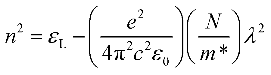
3.2.1 High-frequency dielectric constant (εL). The high-frequency dielectric constant (εL) and carrier concentration (N/m*) were calculated by using the formula43 which involves the dependence between refractive index (n) and wavelength is given by the relation,| |
 | (12) |
where ‘e’ is the electronic charge, ε0 is the permittivity of free space, N/m* is the ratio between no. of charge carriers to their effective masses. These parameters were obtained by considering the lattice vibrational modes and free-electron charge carriers of a system. The εL and N/m* were evaluated from the vertical intercept and slope of the plot between n2 and λ2 presented in Fig. 5d. The εL values showed a decreasing behaviour with laser irradiation. As it is well known that, both the parameters εL and N/m* contributes to the polarization process of the material, the observed changes in these parameters support the promising outcomes of nonlinear optical properties.44 The higher values of εL than that of the ε∞ is due to the change in carrier concentration.
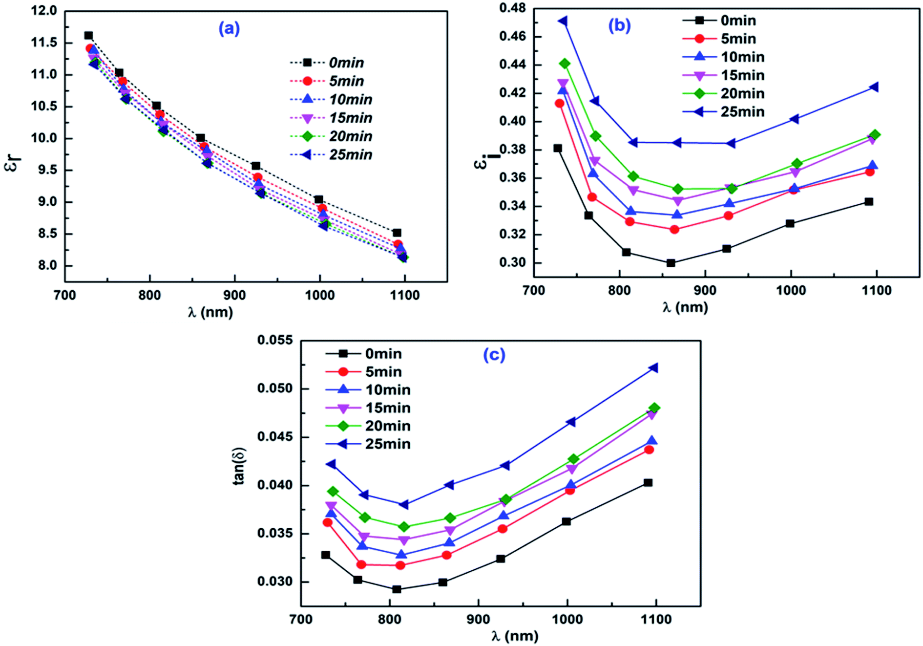
3.2.2 Real and imaginary dielectric constant, dielectric loss factor. The dielectric properties of material play a crucial role in defining the materials polarizability which is suitable for various photonic applications. The complex dielectric constant is given by the relation45 ε* = εr + iεi = (n + ik)2 where εr and εi are the real and imaginary part of the dielectric constant and can be evaluated as the following relation,| | |
εr = n2 − k2 and εi = 2nk
| (13) |
where n and k are the linear refractive index and extinction coefficient of corresponding thin films. The real part (εr) signifies the dispersion of electromagnetic wave traveling inside the material and also responsible for the reduction in its propagation speed whereas the imaginary part (εi) signifies the energy absorbed from the electric field due to dipole motion hence provides an idea regarding the disruptive rate of the wave in the sample.46 Fig. 6a and b represent the corresponding behaviour of the real and imaginary part of dielectric constant with wavelength during the laser irradiation at different time domains. It can be observed that, the values of εr ≫ εi which is due to the dependence of εr mainly on the larger n values than the smaller values of k. The variations in these parameters with wavelength suggest an interaction between the incident photon and free electrons. The behaviour of dielectric parameters with respect to the photo-induced impact during the laser irradiation suggested the decrease in energy dissipated and increase in the disruptive rate of the electromagnetic wave.47 Since εr and εi acts as a mirror of material's optical characteristics, so investigating these parameters is vital for developing/designing the optoelectronic devices. From these real and imaginary part, the dielectric loss of the medium can be obtained by the relation, tan (δ) = εi/εr where δ is the loss angle. This parameter measures the loss rate of mechanical mode power of a dissipative medium.48 In other words, it defines the phase difference of the loss energy at a particular frequency in a sample.49 The loss factor is inversely related to the quality factor which represents the quality of oscillation. The corresponding behaviour of this parameter is presented in Fig. 6c represents a resultant increase in dielectric loss of the medium with the laser irradiation at different time intervals. The laser irradiation maximizes the energy loss during the time domain which is also supported by the obtained behaviour of the extinction coefficient.
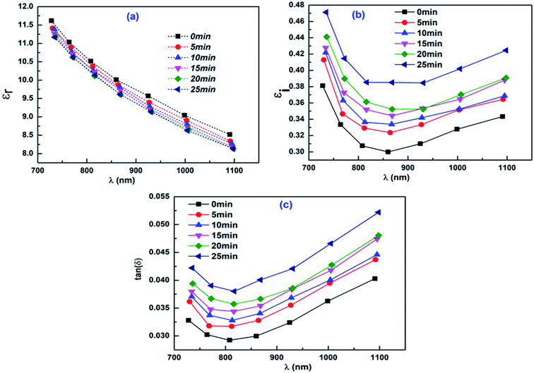 |
| | Fig. 6 (a) εr vs. λ for the film at different irradiation time (b) εi vs. λ for the film at different irradiation time (c) dielectric loss factor at different irradiation time. | |
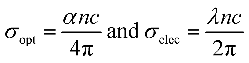
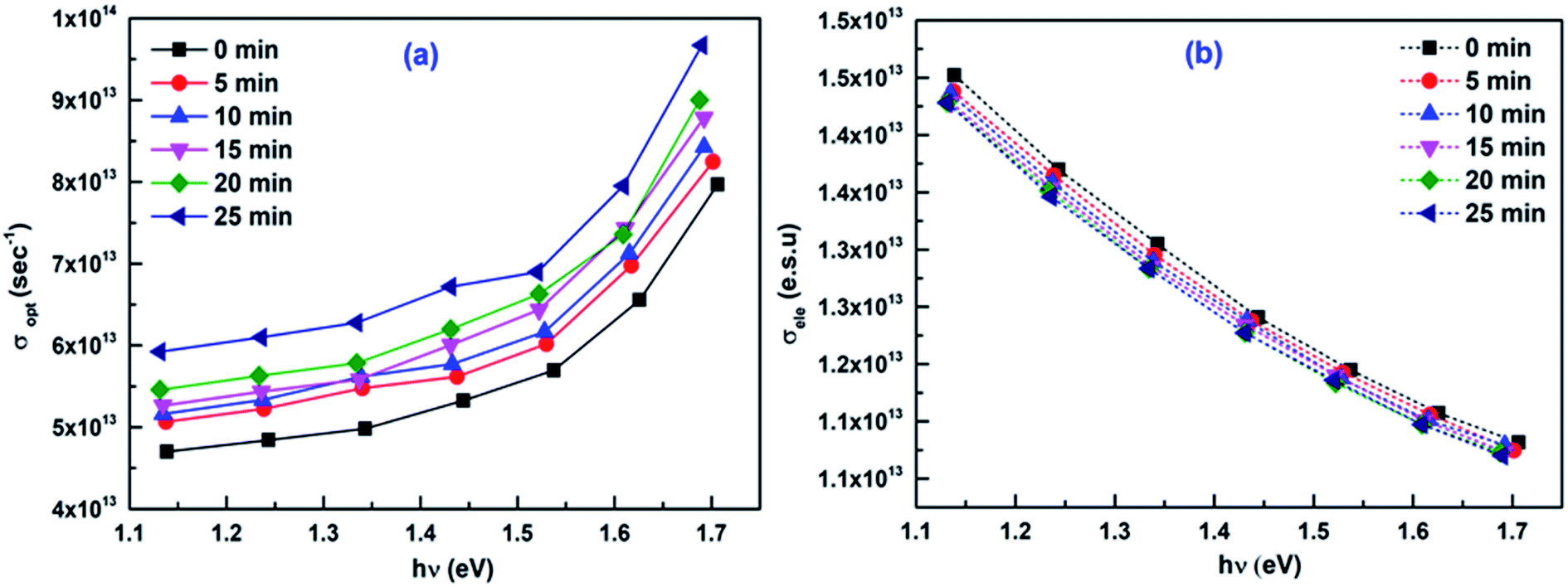
3.3III.3. Optical conductivity (σopt) and electrical conductivity (σelec)
The information regarding the electronic states of the material can be obtained from the measurement of materials optical and electrical conductivity which depends upon the α, n and λ by the relation,50| |
 | (14) |
The σopt represents the conductance of charge carriers due to the optical excitation.51 The variation of these two conductivities at different irradiation time is seen from Fig. 7a and b. The σopt values increased with an increase in laser irradiation time interval whereas the σelec values decreased. The increase in σopt can be justified by the increase in absorption coefficient and density of localized defect states due to the laser irradiation and hence the probability of electron excitation through the band.52 As the σelec inversely related to the absorption coefficient, hence a decreasing behaviour was observed.
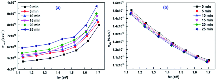 |
| | Fig. 7 Variation of (a) σopt (b) σele at different irradiation time of the studied films. | |
3.4III.4. Nonlinear optical parameters
Nonlinear optical properties of material play an important role in various nonlinear optical devices such as all-optical switching and integrated photonic devices etc. The nonlinear relation between optical parameters and electric field in chalcogenide materials refers to optical nonlinearity. The source of the optical nonlinearity arises due to the nuclear interactions with electronic polarizability (αp) and hence influences bond lengths.53 This phenomenon arises owing to the net polarization developed in materials upon intense exposure to the light beam. The net dipole moment is directly proportional to the susceptibility i.e., P = εo, χ, E where εo stands as permeability of free space and E is the electric field intensity. The susceptibility, χ, is equal to the sum of both linear and nonlinear contribution: χ = χL + χNL where χL = χ(1) denotes the linear part of the susceptibility and χNL = χ(2) + χ(3) is given as the nonlinear part of the susceptibility.
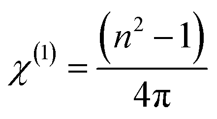
For isotropic medium (in this case the As50Se40Sb10 chalcogenide thin film), the first-order nonlinear optical susceptibility χ(1) can be expressed in terms of linear refractive index by the given relation,54,55
| |
 | (15) |
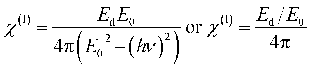
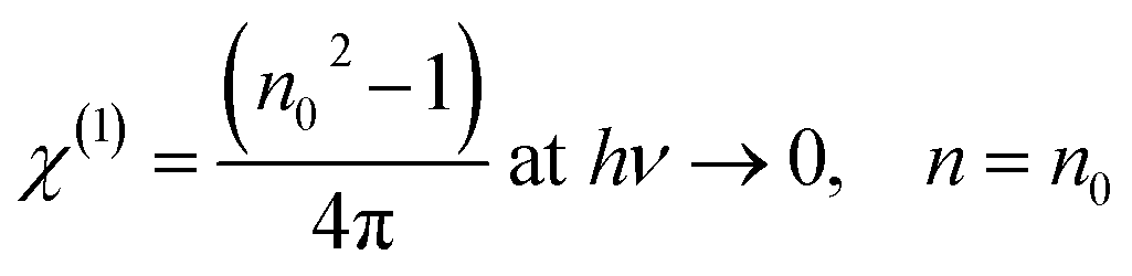
From eqn (15) and the linear refractive index dispersion relation of WDD model i.e. eqn (8), the χ(1) can be expressed as
which becomes
| |
 | (16) |
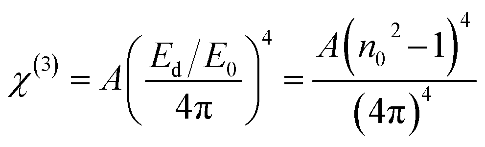
Miller's generalised rule i.e. χ(3) = A(χ(1))4 was used to obtain the third-order nonlinear optical susceptibility χ(3),
| |
 | (17) |
where
n0 is the static refractive index at
hν → 0 and
A is a constant having an estimated value of
A = 1.7 × 10
−10 e.s.u. The decrease in both
χ(1) and
χ(3) with laser irradiation brings down the nonlinearity (
Table 1) in the films which are useful for the stability of the photonic devices. The
χ(3)value of 12.4 × 10
−12 (e.s.u.) for the as-prepared film reduced to 9.76 × 10
−12 and 9.66 × 10
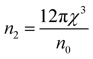
−12 (e.s.u.) for the 20 min and 25 min laser irradiation. So, the difference in the change of values saturates with an increase in irradiation time. The nonlinear refractive index (
n2) was evaluated in terms of
χ(3) by the given relation
| |
 | (18) |
The value of n2 decreased with the time of laser irradiation as shown in Table 1. The n2 value of 1.70 × 10⁻¹⁰ e.s.u. for the as-prepared film reduced to 1.37 × 10⁻¹⁰ and 1.36 × 10⁻¹⁰ e.s.u. for the 20 min and 25 min laser irradiation. The decrease in the value saturates with time which brings control over the fluctuation. Such controlling of n2 value by photoinduced effects is suitable for various modern photonic applications like ultra-fast optical switching, high-speed communication devices, optical limiter, etc.
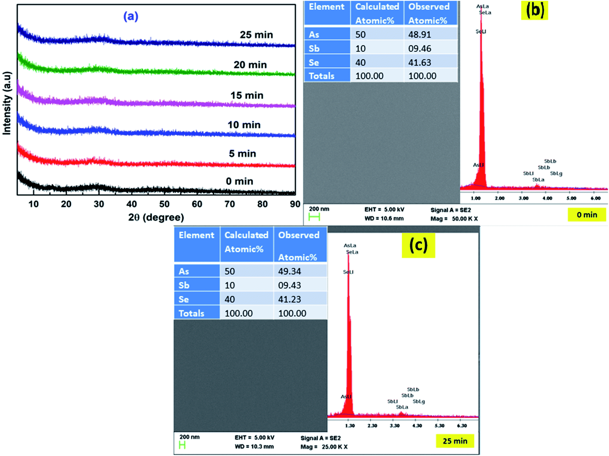
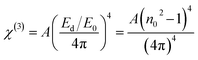
3.5III.5. Structural and morphological study
The photoinduced effect in the As50Se40Sb10 thin films at different irradiation times did not show any noticeable structural change as seen from the XRD patterns (Fig. 8a). The amorphous nature is sustained with laser irradiation. The XRD pattern did not reveal any sharp peaks thus confirming the amorphous nature of the films. The FESEM image of the two laser irradiated films (0 min and 25 min) are shown in Fig. 8b and c. The images clearly show the uniform and homogeneous nature of the films. The presence of the constituent elements like As, Se and Sb in the two films are presented inside Fig. 8b and c. The composition of the films remains nearly the same after laser irradiation and the atomic% of the elements are present in Fig. 8b and c.
 |
| | Fig. 8 (a) XRD patterns for the film at different irradiation time (b) FESEM (inset EDX) image for the 0 min irradiated film (c) FESEM (inset EDX) image for the 25 min irradiated film. | |
4. Conclusion
In summary, we have studied the in situ laser irradiation impact on the linear and nonlinear optical properties of the As50Se40Sb10 thin films at different time period. The kinetics of the bandgap change followed an exponential decay with the decay rate of ∼6.24 min. The fringe strength decreased with irradiation time thus decreasing the oscillator strength of the film. The change in transmittance with laser irradiation caused a significant increase in its absorption coefficient and decrease in refractive index. The increase in the density of states in the gap regime reduced the bandgap (PD) along with the increase in disorder (Urbach energy). The incident laser energy facilitated the LP–LP interaction thus creating more homopolar bonds. The change in the dispersion parameters by photoinduced effect favours for designing high-quality photonic devices as it shows significant changes with laser irradiation. The σopt increased whereas σelec values decreased with laser irradiation time. The real part of the dielectric constant decreased whereas the dielectric loss factor increased with time. The nonlinear refractive index and 3rd order susceptibility decreased and the changes were saturated with time which brings stability in the film properties that is useful for various optical applications.
Author contributions
Deviprasad Sahoo: writing – original draft, software, data curation, investigation, Priyanka Priyadarshini: data analysis, R. Dandela: conceptualization, review and editing, D. Alagarasan: sample preparation, investigation, S. Vardharajperumal: data collection, investigation, R. Ganesan: visualization, investigation, Ramakanta Naik: conceptualization, methodology, writing – review & editing, supervision.
Conflicts of interest
There are no conflicts of interest for this manuscript.
Acknowledgements
The author Dr Naik thank Department of Physics, Indian Institute of Science (IISc.) for Optical, XRD and FESEM measurements.
References
- K. Tanaka, Photo-induced phenomena in chalcogenide glass: comparison with those in oxide glass and polymer, J. Non-Cryst. Solids, 2006, 352, 2580–2584 CrossRef CAS.
- K. Shimakawa, A. Kolobov and S. R. Elliott, Photoinduced effects and metastability in amorphous semiconductors and insulators, Adv. Phys., 1995, 44, 475–588 CrossRef CAS.
- P. Fabbri and M. Messori, Surface modification of polymers chemical, physical, and biological routes, modification of polymer properties, Elsevier, 2017, pp. 109–130 Search PubMed.
- B. J. Eggleton, B. Luther-Davies and K. Richardson, Chalcogenide photonics, Nat. Photonics, 2011, 5, 141–148 CrossRef CAS.
- P. Pradhan, R. Naik, N. Das and A. K. Panda, Band gap tuning in As40Se53Sb07 thin films by 532 nm laser irradiation: an optical investigation by spectroscopic techniques, Opt. Mater., 2018, 75, 699–709 CrossRef CAS.
- A. C. Popta, R. G. DeCorby, C. J. Haugen, T. Robinson, J. N. McMullin, D. Tonchev and S. O. Kasap, Photoinduced refractive index change in As2Se3 by 633 nm illumination, Opt. Express, 2002, 10, 639–644 CrossRef PubMed.
- A. Ganjoo, K. Shimakawa, K. Kitano and E. A. Davis, Transient photodarkening in amorphous chalcogenides, J. Non-Cryst. Solids, 2002, 299–302, 917–923 CrossRef CAS.
- R. Naik, S. Jena, R. Ganesan and N. K. Sahoo, Effect of laser irradiation on optical properties of Ge12Sb25Se63 amorphous chalcogenide thin films, Indian J. Phys., 2015, 89, 1031–1040 CrossRef CAS.
- R. Naik, C. Sripan and R. Ganesan, Photo darkening in As50Se50 thin films by 532 nm laser irradiation, Opt. Laser Technol., 2017, 90, 158–164 CrossRef CAS.
- Q. Liu and F. Gan, Photobleaching in amorphous GeS2 thin films, Mater. Lett., 2002, 53, 411–414 CrossRef CAS.
- A. R. Barik, R. Naik and K. V. Adarsh, Unusual observation of fast photodarkening and slow photobleaching in a-GeSe2 thin film, J. Non-Cryst. Solids, 2013, 377, 179–181 CrossRef CAS.
- V. Lyubin, M. Klebanov, A. Bruner, N. Shitrit and B. Sfez, Transient photodarkening and photobleaching in glassy GeSe2 films, Opt. Mater., 2011, 33, 949–952 CrossRef CAS.
- C. Yan, B.-A. Liu, X. C. Li, C. Liu and X. Ju, Time-dependent photothermal characterization on damage of fused silica induced by pulsed 355-nm laser with high repetition rate, Chin. Phys. B, 2020, 29(2), 027901 CrossRef CAS.
- E. Marquez, J. M. Gonzalez-Leal, R. Prieto-Alcon, R. Jimenez-Garay and M. Vlcek, On the photo and thermally-induced darkening phenomena in As40S40Se20 amorphous chalcogenide thin films, J. Phys. D: Appl. Phys., 1999, 32, 3128 CrossRef CAS.
- R. Naik, S. Jena, R. Ganesan and N. K. Sahoo, Photo-induced optical bleaching in Ge12Sb25S63 amorphous chalcogenide thin films: effect of 532 nm laser illumination, Laser Phys., 2015, 25, 036001 CrossRef.
- A. Ganjoo and H. Jain, Millisecond kinetics of photoinduced changes in the optical parameters of a-As2S3 films, Phys. Rev. B: Condens. Matter Mater. Phys., 2006, 74, 024201 CrossRef.
- K. Antoine, H. Jain and M. Vlcek, Optical spectroscopy of a-As2Se3 under in situ laser irradiation, J. Non-Cryst. Solids, 2006, 352, 595–600 CrossRef CAS.
- S. Ducharme, J. Hautala and P. C. Taylor, Photodarkening profiles and kinetics in chalcogenide glasses, Phys. Rev. B: Condens. Matter Mater. Phys., 1990, 42, 9194 CrossRef CAS PubMed.
- R. Naik, R. Ganesan, K. V. Adarsh, K. S. Sangunni, V. Takats and S. Kokenyesi, In situ pump probe optical absorption studies on Sb/As2S3 nanomultilayered film, J. Non-Cryst. Solids, 2009, 355, 1943–1946 CrossRef CAS.
- A. Zakery and S. R. Elliot, Optical properties and application of chalcogenide glass: a review, J. Non-Cryst. Solids, 2003, 330, 1–12 CrossRef CAS.
- C. Corredor, I. Quiroza, J. Vazquez, J. Galdon, P. Villares and R. Jimenez-Garay, Structural interpretation of the infrared spectrum of a Sb0.05As0.45Se0.50 glassy semiconductor, Mater. Lett., 2000, 42, 229–231 CrossRef CAS.
- E. Akat and G. Aktas, Frequency-resolved photoconductivity studies in amorphous As–Se–Sb, Philos. Mag. B, 2001, 81(7), 689–697 CrossRef CAS.
- A. Dahshan, H. H. Amer, A. H. Moharam and A. A. Othman, Photoconductivity of amorphous As–Se–Sb thin films, Thin Solid Films, 2006, 513, 369–373 CrossRef CAS.
- A. Gadalla, E. R. Shaaban, F. A. Anas, S. Rafique and E. S. Yousef, Resistivity-temperature dependence, thermal and electrical parameters of Se65−xAs35Sbx thin films, Chalcogenide Lett., 2020, 17(5), 229–241 CAS.
- P. Pradhan, P. Khan, J. R. Aswin, K. V. Adarsh, R. Naik, N. Das and A. K. Panda, Quantification of nonlinear absorption in ternary As–Sb–Se chalcogenide glasses, J. Appl. Phys., 2019, 125, 015105 CrossRef.
- R. Naik, A. Jain, E. M. Vinod, R. Ganesan and K. S. Sangunni, Photo induced changes in the optical properties of thermally evaporated As40Se50Sb10 films, Phys. Status Solidi C, 2011, 8, 2785–2788 CrossRef CAS.
- R. Naik, A. Jain, R. Ganesan and K. S. Sangunni, Compositional dependence optical properties study of As40Se60−xSbx thin films, Thin Solid Films, 2012, 520, 2510 CrossRef CAS.
- A. Ganjoo, K. Shimakawa, H. Kamiya, E. A. Davis and J. Singh, Percolative growth of photodarkening in amorphous As2S3 films, Phys. Rev. B: Condens. Matter Mater. Phys., 2000, 62(22), R14601–R14604 CrossRef CAS.
- M. Behera, N. C. Mishra and R. Naik, Thermal annealing induced evolution of Bi3Se2 topological phase from Bi/As2Se3 thin film: structural, optical and morphological study, Phys. B, 2019, 560, 51–59 CrossRef CAS.
- D. Sahoo, P. Priyadarshini, A. Aparimita, D. Alagarasan, R. Ganesan, S. Varadharajaperumal and R. Naik, Role of annealing temperature on optimizing the linear and nonlinear optical properties of As40Se50Ge10 films, RSC Adv., 2020, 20, 26675 RSC.
- N. Barreau, S. Marsillac, J. C. Bern Ede, T. Ben Nasrallah and S. Belgacem, Optical properties of wide band gap indium sulphide thin films obtained by physical vapor deposition, Phys. Status Solidi A, 2001, 184, 179 CrossRef CAS.
- A. S. Hassanien and I. Sharma, Optical properties of quaternary a-Ge15−xSbxSe50Te35 thermally evaporated thin-films: refractive index dispersion and single oscillator parameters, Optik, 2020, 200, 163415 CrossRef CAS.
- J. Tauc, Amorphous and Liquid Semiconductors, Plenum Press, New York, 1979, p. 159 Search PubMed.
- N. F. Mott and E. Davis, Electronics Processes in Non-Crystalline Materials, Clarendon, Oxford, 1979, p. 428 Search PubMed.
- K. Shimakawa, N. Nakagawa and T. Itoh, The origin of stretched exponential function in dynamic response of photodarkening in amorphous chalcogenides, Appl. Phys. Lett., 2009, 95, 051908 CrossRef.
- F. Urbach, The long-wavelength edge of photographic sensitivity and of the electronic absorption of solids, Phys. Rev., 1953, 92, 1324 CrossRef CAS.
- A. S. Hassanien, I. Sharma and A. A. Akl, Physical and optical properties of a-Ge–Sb–Se–Te bulk and film samples: refractive index and its association with electronic polarizability of thermally evaporated a-Ge15−xSbxSe50Te35 thin-films, J. Non-Cryst. Solids, 2020, 531, 119853 CrossRef CAS.
- R. Swanepoel, Determination of the thickness and optical constants of amorphous silicon, J. Phys. E: Sci. Instrum., 1983, 16, 1214 CrossRef CAS.
- A. M. Abd-Elnaiem, A. Z. Mahmoud and S. Moustafa, Structural and optical properties of thermally evaporated and annealed Ge20Se76Sn4 thin films, Opt. Mater., 2021, 111, 110607 CrossRef CAS.
- S. H. Wemple and M. DiDomenico, Behavior of the electronic dielectric constant in covalent and ionic materials, Phys. Rev. B: Condens. Matter Mater. Phys., 1971, 3, 1338 CrossRef.
- A. Sharma and P. B. Barman, An optical study of vacuum evaporated Se85−xTe15Bix chalcogenide thin films, Phys. B, 2010, 405(3), 822–827 CrossRef.
- P. Priyadarshini, D. Sahoo, A. Aparimita, D. Alagarasan, R. Ganesan, S. Varadharajaperumal and R. Naik, Switching of linear and nonlinear optical parameters in As35Se65 thin films upon annealing at both above and below Tg, Appl. Phys. A, 2020, 126, 910 CrossRef CAS.
- M. Behera, N. C. Mishra, R. Naik, C. Sripan and R. Ganesan, Thermal annealing induced structural, optical and electrical properties change in As40Se60−xBix chalcogenide thin films, AIP Adv., 2019, 9, 095065 CrossRef.
- M. El-Nahass, M. H. Ali and I. T. Zedan, Photoinduced changes in linear and non-linear optical properties of Ge10In10Se80 thin films, J. Non-Cryst. Solids, 2014, 404, 78–83 CrossRef CAS.
- L. Tsang, J. A. Kong and K. H. Ding, Scattering of Electromagnetic Waves: Theories and Applications, Wiley, New York, 2004 Search PubMed.
- S. Ikeda and M. Aniya, Correlation between the nonlinear optical constants and the structural relaxation parameters in chalcogenide glasses, J. Non-Cryst. Solids, 2012, 358(17), 2381–2384 CrossRef CAS.
- Q. Shen, K. Katayama, T. Sawada and T. Toyoda, Characterization of electron transfer from CdSe quantum dots to nanostructured TiO2 electrode using a near-field heterodyne transient grating technique, Thin Solid Films, 2008, 516(17), 5927–5930 CrossRef CAS.
- S. Mishra, P. Kumar Singh, R. K. Yadav, A. Umar, P. Lohia and D. K. Dwivedi, Investigation of glass forming ability, linear and non-linear optical properties of Ge–Se–Te–Sb thin films, Chem. Phys., 2021, 541, 111021 CrossRef CAS.
- A. S. Hassanien, Studies on dielectric properties, opto-electrical parameters and electronic polarizability of thermally evaporated amorphous Cd50S50−xSex thin films, J. Alloys Compd., 2016, 671, 566–578 CrossRef CAS.
- M. M. Soraya, Structural and optical properties of Se85−xTe15Inx chalcogenide thin films for optoelectronics, Appl. Phys. A, 2020, 126, 590 CrossRef CAS.
- Q. Liu and X. Zhao, Non-linear optical properties of chalcogenide and chalcohalide glasses, J. Non-Cryst. Solids, 2010, 356(44–49), 2375–2377 CrossRef CAS.
- F. Yakuphanoglu, A. Cukurovali and I. Yilmaz, Refractive index and optical absorption properties of the complexes of a cyclobutane containing thiazolyl hydrazone ligand, Opt. Mater., 2005, 27(8), 1363–1368 CrossRef CAS.
- L. K. Benjamin, P. Dube, C. B. Tabi and C. M. Muiva, Physical, linear and nonlinear optical properties of amorphous Se90−xTe10Mx (M = Zn, In, Pb, x = 0, 5) chalcogenide thin films by electron-beam deposition, J. Non-Cryst. Solids, 2021, 557, 120646 CrossRef CAS.
- H. Ticha and L. Tichy, Semiempirical relation between non-linear susceptibility (refractive index), linear refractive index and optical gap and its application to amorphous chalcogenides, J. Optoelectron. Adv. Mater., 2002, 4(2), 381–386 CAS.
- R. Chauhan, A. K. Srivastava, A. Tripathi and K. K. Srivastava, Linear and nonlinear optical changes in amorphous As2Se3 thin film upon UV exposure, Prog. Nat. Sci.: Mater. Int., 2011, 21, 205–210 CrossRef.
|
| This journal is © The Royal Society of Chemistry 2021 |
Click here to see how this site uses Cookies. View our privacy policy here. 
 Open Access Article
 This Open Access Article is licensed under a Creative Commons Attribution-Non Commercial 3.0 Unported Licence
 *a
*a


 values of the (n2 − 1)−1 vs. (hv)2 plot as shown in Fig. 5b. According to the WDD model, Ed can be represented by an empirical relation i.e., Ed = βNcZaNe where β is a constant, Nc is the effective coordination number of the cation, Za the formal chemical valance of the anion, Ne is the effective number of valence electrons per anion. The value of Ed represents the average strength of interband transition. The Eo represents the separation between the centres' of gravity of the valence and conduction band. Both the parameters show an overall decreasing behaviour with laser irradiation time which represents the impact on the strength of inter-band optical transition and average energy gap of the material.41 The oscillator strength of the material i.e., f = EoEd is presented in Table 1 which shows an overall decreasing behaviour. It indicates the reduction in materials oscillator strength characteristics with an increase in laser irradiation time like the change in fringe position in Fig. 1.