
 Open Access Article
 This Open Access Article is licensed under a
 Creative Commons Attribution 3.0 Unported Licence
Plasmonic enhancement of aqueous processed organic photovoltaics†
R. Chowdhuryab,
L. Teggac,
V. J. Keasta,
N. P. Holmesc,
N. A. Coolingb,
B. Vaughanb,
N. C. Nicolaidisb,
W. J. Belcherb,
P. C. Dastoorab and
X. Zhou *ab
*ab
aDepartment of Physics, School of Mathematical and Physical Sciences, The University of Newcastle, Callaghan, NSW 2308, Australia. E-mail: Xiaojing.zhou@newcastle.edu.au
bCentre for Organic Electronics, Faculty of Science, The University of Newcastle, Callaghan, NSW 2308, Australia
cAustralian Centre for Microscopy and Microanalysis, University of Sydney, NSW 2006, Australia
First published on 25th May 2021
Abstract
Sodium tungsten bronze (NaxWO3) is a promising alternative plasmonic material to nanoparticulate gold due to its strong plasmonic resonances in both the visible and near-infrared (NIR) regions. Additional benefits include its simple production either as a bulk or a nanoparticle material at a relatively low cost. In this work, plasmonic NaxWO3 nanoparticles were introduced and mixed into the nanoparticulate zinc oxide electron transport layer of a water processed poly(3-hexylthiophene):phenyl-C61-butyric acid methyl ester (P3HT:PC61BM) nanoparticle (NP) based organic photovoltaic device (NP-OPV). The power conversion efficiency of NP-OPV devices with NaxWO3 NPs added was found to improve by around 35% compared to the control devices, attributed to improved light absorption, resulting in an enhanced short circuit current and fill factor.
1 Introduction
To meet the environmental, socio-economic and ethical sustainability demands of a future energy system necessarily requires that this energy system be renewable and sustainable.1,2 Within this framework, solar energy (compared to other sources of renewable energy) offers a cost effective, non-polluting, sustainable, silent solution that has the capacity to supply efficient power at large scale.3 Over the past few decades, organic photovoltaics (OPVs), based on the bulk-heterojunction (BHJ) structure, have been developed into a promising technology due to their intrinsically low manufacturing cost and eco-friendly fabrication process through roll-to-roll printing techniques.4,5 Additionally, several life cycle cost analysis reports have confirmed the ability of OPV technology to contribute cost-effectively to the global energy supply.6,7The main drawback of current BHJ-OPV technology is the synthesis of the photo-active layer from hazardous chlorinated and/or aromatic solvents such as chloroform (CF), chlorobenzene (CB) and dichlorobenzene (DCB). In response to these concerns, researchers have been working on non-toxic or ‘green’ solvent ink formations for OPV application.8–11 Non-toxic solvents, in particular, aqueous nanoparticulate organic photovoltaics (NP-OPV) have been investigated in our group since last ten years and the device efficiency has steadily increased from 1.4% to 3.3%.12–15 Other research groups using different donor–acceptor materials have reported NP-OPV device performance in the range of 1.9% to 3.8%.16,17 More recently, the efficiency of aqueous NP-OPV devices has reached 7.5% through the use of removable surfactants.18
Nevertheless, aqueous processed OPVs are still much less efficient than those of conventional BHJ OPVs. Previous work to improve device efficiency has focussed on investigating the donor–acceptor mixed NP domain morphology and its associated photo-physics.19 This research identified the origin of the poor performance of these NP-OPV devices to be: (1) the presence of excess surfactant in the photoactive layer; (2) poor wetting of aqueous nanoparticle inks resulting in low film quality in the photoactive layer; (3) improper distribution of the donor and acceptor material domains in the photoactive layer, leading to poor charge generation.18,20
A number of studies have already been undertaken to address these issues. For instance, removing the excess of surfactant from the NP ink and forming better quality of films by optimising the dialysis strategy and utilising the thermal treatment has been reported.18,21 In addition, a new rapid evaporation technique was introduced by Marks et al. to form highly intermixed donor–acceptor film morphology.22 However, the issue of poor charge generation in NP-OPV devices has yet to be addressed and requires, through careful nanoscale engineering, the development of new NP-OPV structures that are able to enhance charge generation and extraction.
Due to the low carrier mobility of conducting polymers23 and short exciton lifetime,24 the optimal thickness of the active layer of BHJ-OPVs is limited to 100 nm or less.25–27 Hence, this thin active layer limits the light absorption and consequently affects the photo-conversion efficiency. The introduction of plasmonic NPs into BHJ-OPVs is commonly used to improve their light absorption and charge generation by enhancing the light scattering either within the active layer or at the active layer/electrode interface, which in turn increases the length of the optical path thus improving light absorption in the photoactive layer.28–32 Moreover, plasmonic nanoparticles can be made into a suspension that is compatible with the solution processing techniques used for BHJ-OPV fabrication.33–35 To date, a number of different plasmonic nanoparticles, such as Au, Ag, graphene oxide with Au spheres, etc., have been reported as plasmonic nanoparticles for BHJ-OPVs.36–38
Recent work has assessed the feasibility of NaxWO3 as an alternative plasmonic material since it exhibits strong plasmonic resonances compared to Au and offers simple nanofabrication at low cost.39,40 In this work, plasmonic structured NP-OPV devices have been fabricated to study the light–matter interaction in the nanoscale region between metal oxide plasmonic nanoparticle and water processed photo-active layer. A combination of microscopic and film physical/chemical spectroscopic techniques have been used to elucidate the multilayer film morphology of NaxWO3 NP-OPV devices and the effect of plasmonic nanoparticles on their performance.
2 Experimental details
2.1 Synthesis of NaxWO3 nanoparticles
NaxWO3 nanoparticles were prepared using a modification of furnace-assisted method of Straumanis,41 as described previously.42 Briefly, powders of sodium tungstate dihydrate (Na2WO4·2H2O, VWR, >99%), tungsten(VI) oxide (WO3, Sigma-Aldrich, 99.9%) and tungsten (Aldrich, ≥99.9%) were mixed proportionally to target x = 0.81. The powders were crushed and mixed using mortar and pestle, pressed under ≈20 MPa into a pellet, then heated in a vertical tube furnace at 875 °C for 3 min under flowing N2. The sample was then milled in a high-energy ball mill for 1 h, with a 1![[thin space (1/6-em)]](https://www.rsc.org/images/entities/char_2009.gif) :5 charge ratio of 2–5 mm steel balls. X-ray diffraction (XRD) patterns of the NaxWO3 nanoparticles were collected using a Philips X'Pert MPD XRD fitted with a Cu Kα anode. Patterns were collected across 5° ≤ 2θ ≤ 90° in 0.013° steps, with a total acquisition time of ≈60 min. From the Rietveld analysis of the patterns, the sample purity was determined using the method of Hill and Howard,43 and the Na content of the NaxWO3 phase was found using the relationship of Brown and Banks.44
:5 charge ratio of 2–5 mm steel balls. X-ray diffraction (XRD) patterns of the NaxWO3 nanoparticles were collected using a Philips X'Pert MPD XRD fitted with a Cu Kα anode. Patterns were collected across 5° ≤ 2θ ≤ 90° in 0.013° steps, with a total acquisition time of ≈60 min. From the Rietveld analysis of the patterns, the sample purity was determined using the method of Hill and Howard,43 and the Na content of the NaxWO3 phase was found using the relationship of Brown and Banks.44
2.2 P3HT:PC61BM photoactive nanoparticle synthesis
Poly(3-hexylthiophene) (P3HT) (Mn 20 kDa) and PC61BM were synthesised in house (Centre for Organic Electronics, University of Newcastle, Australia) according to literature.45,46 Sodium dodecyl sulphate (SDS) with 98% purity was purchased from Sigma-Aldrich. PEDOT:PSS (AI4083) was purchased from Heraeus, Germany and filtered through a 0.45 μm PVDF filter before use. 15 mg of P3HT polymer donor material and 15 mg of PC61BM fullerene acceptor material were mixed in 560 μl of anhydrous chloroform and stirred at 500 rpm, 35 °C for 25 min on a hotplate to form organic phase. The aqueous phase was prepared by mixing 33 mg of sodium dodecyl sulphate (SDS) surfactant in 2800 μl of filtered Milli-Q water using stirring condition of 500 rpm for 25 min at room temperature. After that the organic and aqueous phases were mixed to form a macroemulsion and then generate a miniemulsion using Hielscher UP400S (ultra-horn sonication) at 50% amplitude for 2 minutes with a surrounding ice bath in place (to dissipate produced heat during sonication). The miniemulsion was then transferred immediately into the pre-set hotplate (stirrer at 1200 rpm, 60 °C) for overnight to evaporate the chloroform from the emulsion droplets to form the nanoparticle dispersion. Next, the dispersion was placed by pipette into the Hettich Zentrifugen Rotina 420 centrifugal dialysis to remove excess surfactant as well as concentrate the nanoparticle inks following the same procedure reported in our previous work to get an ink solid loading of 6 wt%.152.3 Microscopy
For scanning electron microscopy (SEM) analysis, NaxWO3 nanoparticles were mixed with ZnO in ethanol and SEM samples were prepared by spin coating of 70 μl of the mixture onto glass substrates at 5000 rpm for 1 min. Another sample of mixture of NaxWO3 nanoparticles and ZnO on aluminium sheet was prepared by drop cast of solution to collect the energy dispersive spectrometer (EDS) data. A Zeiss Sigma VP Field Emission SEM (FESEM) was used under 15 kV beam, using back scattering electron detector and magnification ranges of 5k–50k×. High-magnification transmission electron microscopy (TEM) (JEOL JEM-2100 LaB6) instrument also was used to observe the morphology of the ZnO and NaxWO3 NP mixture as well as to collect the local EDS element mapping to validate that the mixture contains both ZnO and NaxWO3 nanoparticles. The acceleration voltage was 200 kV. The TEM sample also prepared by drop cast process on lacey Cu grid and dried the solution in ambient environment. The drop casting of nanoparticles on lacey Cu grid run 2–3 times to confirm enough nanoparticles on grid.Atomic force microscopy (AFM) images were collected using an Asylum Research Cypher in AC mode. Soft tapping mode Tap150Al-G AFM tips were supplied by Budget Sensors with resonant frequency of 150 kHz and force constant: 5 N m−1. Bare ZnO and mixture of NaxWO3 plasmonic nanoparticles with ZnO nanoparticle films were coated onto glass substrates for AFM analysis.
2.4 Spectroscopy
To measure the UV-vis spectrum, an ultraviolet-visible absorption spectrophotometer (UV Vis, Varian Cary 6000i) with an integrating sphere was used in the wavelength range of 200–1200 nm in 1 nm step, with a deuterium plasma lamp for the 200–350 nm range, and a tungsten halogen lamp used for the 350–1200 nm range. For photoluminescence (PL) measurements, Shimadzu RF-6000 spectrofluorophotometer with a beam to sample angle of 65°, λexc = 550 nm, λem = 400–900 nm, excitation bandwidth of 5 nm and emission bandwidth of 10 nm was used. A 420 nm high-pass cut-off filter was placed in the path of the beam before the sample. All samples for UV Vis and PL were kept as the same structure of NP-OPV devices (without Al layer).2.5 Device fabrication
To fabricate the NP-OPV devices, pre-cleaned (by water, acetone and isopropanol for 10 minutes) patterned Indium Tin Oxide (ITO) substrates were treated by UV–ozone cleaner for 20 minutes. PEDOT:PSS (AI4083) films of 33 ± 6 nm thickness were spin coated onto ITO at 5000 rpm (1 min) and then dried on a hotplate at 150 °C, 20 min. After that, the PEDOT:PSS coated ITO substrates were treated 10 min into the UV–ozone cleaner. Then, P3HT:PC61BM NP ink (35 μl) was spin-coated at 2000 rpm for 1 min and baked for 5 min at 110 °C. The thickness of the photoactive layer was 103 ± 7 nm. Then, ZnO/ZnO:NaxWO3 films were deposited at 5000 rpm for 1 min and dried at 110 °C for 5 min in nitrogen glove box. The thickness of ZnO/ZnO:NaxWO3 layers were measured with an average thickness of 15 ± 6 nm. Finally, Al (thickness: 100 nm) electrodes were deposited under vacuum conditions (10−6 torr) via thermal evaporation using an Angstrom Amod deposition system.
2.6 Device characterisation
The current density–voltage (J–V) measurements of fabricated NP-OPV devices were conducted using a Newport Class A solar simulator with an AM 1.5 spectrum filter. The light intensity was measured to be 100 mW cm−2 by a silicon reference solar cell (FHG-ISE) and the J–V data were recorded with a Keithley 2400 Source Meter. The NP-OPV devices were masked during testing under AM 1.5 conditions where the masked area was 4 mm2. For the device performance, it is reported as the average value ± standard deviation which were calculated from 12 devices based on two substrates with the value for the best devices in the bracket.3 Results and discussion
3.1 Characterisation of NaxWO3 and ZnO![[thin space (1/6-em)]](https://www.rsc.org/images/entities/h3_char_2009.gif) :NaxWO3 mixed nanoparticles
:NaxWO3 mixed nanoparticles
The light absorption spectra of NaxWO3 nanoparticles coated on a quartz substrate is presented in Fig. 1a. There are two distinct visible and near infrared absorption features arising from the NaxWO3 plasmonic material, at ∼630 nm and ∼1045 nm, corresponding to the excitation of localised surface plasmonic resonances (LSPR) of NaxWO3.47 The strong but narrow absorption peak at ∼230 nm in the ultraviolet (UV) range is attributed to the inter-band transition of NaxWO3 plasmonic nanoparticle.39 The transmission electron microscopy (TEM) image shown in Fig. 1b indicates that the size of nanoparticles is of the order of tens of nanometres. Fig. 1c shows an XRD pattern of the NaxWO3 nanoparticles after ball-milling. Overall, the refined model is a good fit to the measured data. From quantitative phase analysis, the sample was found to be ≈99 mol% NaxWO3, and ≈1 mol% W and Fe impurity. From the refinement of the NaxWO3 lattice parameter, a = 3.8508(1) Å, the Na content was found to be x = 0.81.
 | ||
Fig. 1 (a) UV-vis spectrum of NaxWO3 nanoparticle film. (b) The TEM image of NaxWO3 nanoparticle with 50 nm scale bar. (c) XRD pattern and Rietveld refinement of NaxWO3 nanoparticles. The black dots show the data, the red line shows the Rietveld model, and the green line is the difference between the two. Peaks of NaxWO3 are indexed according to the Pm![[3 with combining macron]](https://www.rsc.org/images/entities/char_0033_0304.gif) m structure of Straumanis.41 The blue dashes indicate the peaks included in the model, from top to bottom corresponding to NaxWO3,44 BCC Fe and BCC W. m structure of Straumanis.41 The blue dashes indicate the peaks included in the model, from top to bottom corresponding to NaxWO3,44 BCC Fe and BCC W. | ||
The back-scattered SEM image of a drop-cast ZnO:NaxWO3 mixture on aluminium sheet is shown in Fig. 2a, with the NaxWO3 nanoparticles clearly visible (marked by arrow sign and circle) as bright objects with respect to background. The EDS spectra (Fig. 2b) clearly show that tungsten is present in the mixture, along with zinc, oxygen and aluminium; consistent with well-mixed ZnO and NaxWO3 plasmonic nanoparticles deposited on an aluminium substrate. The small peaks at about 6.39 keV correspond to the Kα peak of iron; consistent with the low levels of iron impurity identified in the XRD analysis. Moreover, the Zn Lα and Na Kα peaks are overlapped as observed in Fig. 2b, therefore the obtained elemental composition of 31% around 1 keV would be the summation of both elements. However, clear EDS peaks of Zn Kα and W M indicate presence of both Zn and Na in NaWO3. High-magnification transmission electron microscopy (TEM) imaging and corresponding Zn and W element EDS mappings of the ZnO:NaxWO3 mixture are shown in Fig. 2c–e. The images show a nanoparticulate aggregate within the ZnO:NaxWO3 mixture, with a NaxWO3 (Fig. 2e) core region surrounded by a ZnO coating (Fig. 2d).
 | ||
| Fig. 2 (a) Backscattering detector scanning electron microscopy (BSD-SEM) image of ZnO:NaxWO3 mixture nanoparticles where ZnO:NaxWO3 solution drop casted on Al sheet substrate. The NaxWO3 nanoparticles mixed with ZnO clearly observed in the SEM image those were marked by red arrows and circles. (b) Energy dispersive X-ray spectrum (EDS) of the SEM scanned area indicates the composition of Na, Zn, O and W which confirms the proper mixing of NaxWO3 nanoparticles into the ZnO. (c) High-magnification transmission electron microscopy (TEM) image of the drop cast ZnO:NaxWO3 mixture nanoparticles was presented along with EDS mapping of (d) Zn and (e) W elements. | ||
3.2 Performance of plasmonic NP-OPV devices
The architecture of the control NP-OPV device (ITO/PEDOT:PSS/NP-P3HT:PC61BM/ZnO/Al) the plasmonic NP-OPV device (ITO/PEDOT:PSS/NP-P3HT:PC61BM/NaxWO3:ZnO/Al) is shown in Fig. 3a and b, respectively. The NaxWO3:ZnO weight ratios (dispersed in ethanol) were 0, 0.35, 0.40, 0.45, 0.50.
 | ||
| Fig. 3 Schematic diagrams of the device architecture (a) control NP-OPV device and (b) NaxWO3 plasmonic NP-OPV device. | ||
The performance of the ITO/PEDOT:PSS/NP-P3HT:PC61BM/NaxWO3:ZnO/Al OPV devices (device A to E) for the five different NaxWO3:ZnO ratios are presented in Fig. 4a–f with the device performance statistics summarised in Table 1. By systematically varying the NaxWO3:ZnO weight concentration ratios in the suspension based on Table 1 (device A to E), the corresponding device PCEs (Fig. 4a) improved from 1.25 ± 0.09% (1.32%) (device A NaxWO3:ZnO = 0) to 1.42 ± 0.05% (1.58%) in NP-OPV (device B NaxWO3:ZnO = 0.35) before maximising at 1.60 ± 0.09% (1.78%) (device C NaxWO3:ZnO = 0.4). The improvements (corresponding to a ∼17% and ∼35% increase in PCE for device B and C, respectively) originate primarily from an increased FF (Fig. 4c) and JSC (Fig. 4d). In particular, for device B, the FF and JSC increase from 0.48 to 0.51 and JSC from 6.64 mA cm−2 to 7.20 mA cm−2, respectively, whereas for device C, the FF and JSC increase from 0.48 to 0.53 and 6.64 mA cm−2 to 7.47 mA cm−2 correspondingly. It should be noted that, for device A (control), the 10 mg ml−1 of ZnO weight concentration has been optimized to achieve the best OPV device performance.48 Therefore, any device performance enhancement cannot be due to the change of ZnO weight concentrations.
 | ||
| Fig. 4 (a) Average power conversion efficiency, (b) average open circuit voltage (VOC), (c) average fill factor (FF), (d) average short circuit current density (JSC) and (e) current density–voltage (J–V) curves of NP-OPV devices with (NP-OPV devices from B to E) and without (NP-OPV device A) NaxWO3 nanoparticles. (f) The external quantum efficiency of the best NaxWO3 NP-OPV device C compared with the control NP-OPV device A. | ||
| Name of NP-OPV | Weight concentration (mg ml−1) | PCE (%) | VOC (V) | FF (%) | JSC (mA cm−2) | |
|---|---|---|---|---|---|---|
| NaxWO3 | ZnO | |||||
| A | 0 | 10 | 1.25 ± 0.09 | 0.41 ± 0.01 | 0.47 ± 0.02 | 6.47 ± 0.48 |
| (1.32) | (0.41) | (0.48) | (6.64) | |||
| B | 3.5 | 6.5 | 1.42 ± 0.05 | 0.42 ± 0.01 | 0.50 ± 0.02 | 6.80 ± 0.16 |
| (1.58) | (0.43) | (0.51) | (7.20) | |||
| C | 4 | 6 | 1.60 ± 0.09 | 0.43 ± 0.01 | 0.51 ± 0.02 | 7.29 ± 0.31 |
| (1.78) | (0.45) | (0.53) | (7.47) | |||
| D | 4.5 | 5.5 | 0.83 ± 0.26 | 0.36 ± 0.05 | 0.39 ± 0.07 | 5.80 ± 0.63 |
| (1.22) | (0.41) | (0.47) | (6.33) | |||
| E | 5 | 5 | 0.74 ± 0.17 | 0.36 ± 0.04 | 0.37 ± 0.07 | 5.64 ± 0.59 |
| (0.93) | (0.39) | (0.40) | (5.95) | |||
Further increases of the NaxWO3:ZnO ratio had a negative effect on NP-OPV performance; for device D (NaxWO3:ZnO = 0.45) and device E (NaxWO3:ZnO = 0.5) the PCE dropped to 0.83 ± 0.26% (1.22%) and 0.74 ± 0.17% (0.93%), respectively. Devices A to C show no noticeable changes in the trend of VOC as presented in Fig. 4b. By contrast, for NaxWO3:ZnO ratios above 0.4, the PCE starts to decrease as shown in Fig. 4a, due to decreases across VOC, FF and JSC (Fig. 4b–d). The external quantum efficiency (EQE) spectra of best NP-OPV device (device C) in comparison with the control NP-OPV (device A) device are presented in Fig. 4f. Device C exhibits higher EQE compared to device A across the entire spectral range; consistent with the JSC data.
3.3 Effect of NaxWO3 on device performance
To investigate the origin of device performance enhancement of NaxWO3 nanoparticle embedded aqueous NP-OPV devices, microscopy and spectroscopy have been used to examine the film quality and the morphological distribution of the plasmonic NP in the overall electron transport layer (ETL). The back scattering SEM images of bare ZnO and NaxWO3:ZnO films are shown in Fig. 5, with the bright particles (with respect to the background) corresponding to NaxWO3 nanoparticles. Fig. 5a reveal a very smooth bare ZnO film whereas Fig. 5b and c show that for NaxWO3:ZnO ratios of 0.35 and 0.4, the surface contains an increasing number of NaxWO3 NPs that are evenly distributed within the ZnO film. For NaxWO3:ZnO ratios of 0.45 (Fig. 5d) and 0.5 (Fig. 5e), NaxWO3 NPs aggregates (marked as red arrow signs) start to appear in the SEM images. The presence of aggregated NaxWO3 nanoparticles in the ZnO ETL would have a detrimental effect on the morphology of the ZnO ETL and, consequently, on the film quality of the subsequently deposited aluminium electrode. As such, the observation of NaxWO3 NP aggregates at NaxWO3:ZnO ratios above 0.4 is entirely consistent with the decreased device performance observed for devices with higher NaxWO3 loadings.
 | ||
| Fig. 5 SEM images of mixture of films (prepared on glass substrates) with (a) 0 mg ml−1, (b) 3.5 mg ml−1, (c) 4 mg ml−1, (d) 4.5 mg ml−1 and (e) 5 mg ml−1 weight concentration of NaxWO3 in ZnO. All of the SEM images are collected using back scattering electron detector. The scale bar is 10 μm. | ||
Atomic force microscopy (AFM) has also been used to examine the morphology of a control ZnO film (Fig. 6a), and NaxWO3:ZnO films with weight ratios of 0.4 (Fig. 6b) and 0.5 (Fig. 6c). In addition, to compare the effect of optimal (NaxWO3:ZnO = 0.4) and highest NaxWO3 NP concentration (NaxWO3:ZnO = 0.5) of NaxWO3 on ZnO film, the 3D views of the films are illustrated in Fig. 6d–f. The morphology of bare ZnO film (Fig. 6a) is very smooth, consistent with the SEM image (Fig. 5a) and the surface root-mean-square (RMS) roughness is very small (0.5 ± 0.1 nm). By comparison, the roughness of the NaxWO3:ZnO = 0.4 film increases to 2.5 ± 2.1 nm. However, the distribution of NaxWO3 nanoparticles in the NaxWO3:ZnO = 0.4 film (Fig. 6b–e) is uniform, with well separated NPs showing no significant aggregation in the 3D image (Fig. 6e); consistent with the corresponding SEM image (Fig. 5c). By contrast, the surface of NaxWO3:ZnO = 0.5 film is rougher (RMS 5.5 ± 3.4 nm) with more densely packed NaxWO3 nanoparticles and larger aggregates observed in 3D view (Fig. 6f); consistent with the observation in Fig. 5e. Typical surface height profiles for the three films are presented in Fig. 6g–i, with average NPs heights of 2.7 ± 0.4 nm, 12 ± 11 nm and 28 ± 20 nm for the NaxWO3:ZnO = 0, 0.4 and 0.5 films, respectively. The AFM data supports the SEM observation that for NaxWO3:ZnO ratios above 0.4, the NaxWO3 plasmonic nanoparticles start to aggregate and form larger surface structures with dimensions that are large enough to completely penetrate into the aqueous photoactive layer and degrade of device performance. In addition, the increased roughness at ZnO/Al interface can also deteriorate electron transport within NP-OPV device again leading to lower device performance. Therefore, the device performance starts to drop at NaxWO3:ZnO ratios above 0.4. The AFM morphology of the NaxWO3:ZnO = 0.35 and NaxWO3:ZnO = 0.45 samples provide further support for this observation (Fig. S1, ESI†).
 | ||
| Fig. 6 (a)–(c) Show the AFM images (5 μm × 5 μm) of ZnO films with NaxWO3:ZnO concentration ratios of 0, 0.4 and 0.5, respectively. (d)–(f) Show the corresponding 3D images of (a)–(c). (g)–(i) Typical surface height profiles of the NaxWO3 nanoparticles observed in (a)–(c) with respect to the X-axis. | ||
The UV-vis absorption spectra of the ZnO and the optimal NaxWO3:ZnO ratio (0.4) films on quartz substrates are presented in Fig. 7a. It clearly shows the light absorption arising from the NaxWO3 NPs across the visible to near infrared regions compared to the ZnO only film and matches the light absorption spectra of the pure NaxWO3 film shown in Fig. 1a. The UV-vis data confirms that the NaxWO3:ZnO film consists of well-mixed NaxWO3 nanoparticles within the ZnO layer; consistent with the EDS data in Fig. 2. The absorption spectra of the PEDOT:PSS/NP-P3HT:PC61BM/ZnO multilayer films with and without NaxWO3 nanoparticles are presented in Fig. 7b, where the light absorption in the near infrared range (650–800 nm) is presented as an inset. Sample A to E follow the same NaxWO3:ZnO ratios described in Table 1. The effect of the NaxWO3 plasmonic enhancement on the light absorption is most clearly visible for samples B and C. As the weight concentration of NaxWO3 NPs in the ZnO film is increased, the light absorbance of sample B and C across the visible region is enhanced by around 9% and 15%, respectively, compared to the control sample A. This increased light absorption explains the enhanced photocurrent in the plasmonic nanoparticle embedded NP-OPV devices of B and C over the control NP-OPV device. The higher scattering background in the near infrared range of 650 to 800 nm (inset) for samples B and C is also consistent with a plasmonic enhancement due to light scattering. Furthermore, the overall light absorption of the plasmonic nanoparticle embedded films for sample D and E decreases by around 1% (sample D) and 11% (sample E) as the NaxWO3:ZnO ratio increases to 0.45 and 0.5, respectively, again in good agreement with the variation of the photocurrent density.
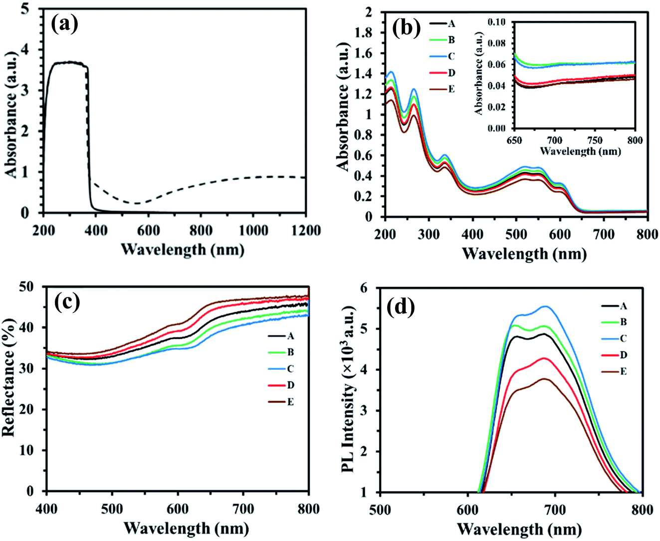 | ||
| Fig. 7 Light absorbance spectra of (a) ZnO:NaxWO3 film (dash line) and ZnO film (solid line). (b) The light absorbance spectrum of PEDOT:PSS/P3HT:PC61BM NP/ZnO films A to E, the inset figure expands and highlights the light absorbance spectra in the higher wavelength of visible region. (c) The total light reflectance (specular and diffuse reflectance) spectra and (d) photoluminescence (PL) spectra of the PEDOT:PSS/P3HT:PC61BM NP/ZnO films for the control multilayer sample A and PEDOT:PSS/P3HT:PC61BM NP/ZnO:NaxWO3 samples B to E. | ||
To further probe the effect of the higher NaxWO3 weight concentrations on light absorption, the total (specular plus diffuse) light reflectance spectrum of PEDOT:PSS/NP-P3HT:PC61BM/ZnO:NaxWO3 multilayer films were collected and are presented in Fig. 7c. Samples D and E exhibit higher reflectivity across the entire 400–800 nm spectral range, consistent with decreased light absorption32,49 arising from the increased aggregation of the NaxWO3 NPs observed for these samples; resulting in a reduced plasmonic enhancement of their surrounding electric field.50 Moreover, as the aggregated NPs are large enough (peak heights > 50 nm observed in Fig. 6i) to penetrate the active layer, it is likely that the morphology of the water processed P3HT:PC61BM nanoparticle based photoactive layer is also degraded; decreasing the light absorption capacity of these multilayer films D and E. By contrast, the spectrum-wide lower reflectivity of the lower NaxWO3:ZnO ratio samples (B and C) is consistent with increased light absorption arising from the plasmonic enhancement of the NaxWO3 NPs.
The photoluminescence (PL) spectra of the PEDOT:PSS/NP-P3HT:PC61BM/ZnO (NaxWO3) multilayer films are presented in Fig. 7d in order to investigate the effect of NaxWO3 nanoparticles on exciton generation. The incorporation of the NaxWO3 plasmonic NPs leads to broader PL spectra and an increase of the PL intensity by ∼8% for the multilayer film B and by ∼13% for the multilayer film C compared to the control multilayer film A. The broadening and enhancement of the PL intensity can be attributed to the fact that the LSPR excitation and light scattering of the NaxWO3 plasmonic nanoparticles inside the device increase the degree of light collection, thereby, leading to an enhanced light excitation generation rate.51 Moreover, the enhanced PL intensity arises from the strong coupling between the excitonic state of the polymer and the plasmonic field of the NaxWO3 nanoparticles, which is due to the oscillation of the surface plasmonic dipole electric field and excitons.52 Thus, it can be concluded that the incorporation of NaxWO3 nanoparticles significantly enhances the exciton generation, rate as observed in multilayer films B and C. However, further increasing the NaxWO3 nanoparticles weight concentration in the ZnO results in the aggregation of nanoparticles, as is evident in the SEM images of multilayer films D and E (Fig. 5d and e). As a result, the electric field intensity starts to decay with the increase of nanoparticle aggregate size, leading to a reduction in the LSPR excitation effect of the plasmonic materials, as well a decrease in the PL intensity of the multilayer film, as shown in Fig. 7d, which is consistent with the UV-vis spectra of the corresponding multilayer films D and E.
To further validate the effect of NaxWO3 nanoparticles on the exciton generation and dissociation of the NP-OPV devices, the maximum exciton generation rate (Gmax) and the exciton dissociation probability (P[E,T]) are considered for the hero NP-OPV device C with respect to control NP-OPV device A, following a previously reported method.32,53,54 The dependence of the photocurrent density (Jph) on the effective voltage (Veff) is shown in Fig. 8a for NP-OPV device A and NP-OPV device C. Herein, Jph is calculated by the following formula:
| Jph = JL − JD | (1) |
 | ||
| Fig. 8 (a) Jph vs. Veff curves and (b) P[E,T] vs. Veff curves of the NP-OPV devices with (NP-OPV device C) and without (NP-OPV device A) NaxWO3 plasmonic nanoparticles. | ||
Veff is described by the following equation:
| Veff = V0 − Va | (2) |
| Jsat = qGmaxL | (3) |
| Jph = qGmaxP[E,T] | (4) |
The corresponding values of P[E,T] at any effective voltage (Veff) can be attained from the plot of the normalized photocurrent density Jph/Jsat. The calculated Jph values at Va = 0 were 4.88 mA cm−2 and 6.40 mA cm−2 resulting in P(E,T) of around 75% and 80%, for the control (NP-OPV device A) and best NaxWO3 (NP-OPV device C) devices, respectively. These results demonstrate that the presence of the NaxWO3 nanoparticles in the NP-OPV structure directly increases the dissociation of excitons into free carriers.
For the best of our knowledge, our work is the first study using plasmonic nanoparticles, in particular, a plasmonic material other than Au or Ag nanostructures, in aqueous processed OPV devices. We put a summary of literature in Table 2 that shows different types of plasmonic nanostructures used in bulk heterojunction (BHJ) OPV devices and compare them with our aqueous processed OPV work. The enhancement due to the plasmonic nanostructure observed in this work is comparable to those studies. It also should be noted that the previous studies in our group have showed that the aqueous processed OPV devices behave very differently from the conventional BHJ OPV devices.12–15 This work points a future direction to further explore NaxWO3 nanoparticles in the OPV applications.
| Plasmonic structure | Location of plasmonic structure | Proposed mechanism | PCE (%) | JSC (mA cm−2) | Enhancement (%) | |
|---|---|---|---|---|---|---|
| PCE | JSC | |||||
| Au nano-rods32 | ETL | Scattering | 8.01 (7.43) | 17.17 (16.27) | 7.8 | 5.5 |
| Fe3O4 NPs33 | Photoactive layer | Scattering | 2.22 (1.09) | 8.62 (7.74) | 104 | 11 |
| Au–Ag nano-cube35 | HTL | Electric field and scattering | 3.10 (2.85) | 8.70 (8.40) | 8.8 | 3.6 |
| Au NPs36 | HTL | LSPR | 4.19 (3.48) | 10.18 (8.95) | 20 | 14 |
| Au spheres and Au rods37 | HTL | Scattering and LSPR | 4.28 (3.46) | 11.49 (9.28) | 24 | 24 |
| Au spheres and GO composites38 | HTL | Near field effect | 3.98 (3.25) | 10.44 (9.37) | 22 | 11 |
| Au nano-arrows56 | ETL | Scattering and LSPR | 7.82 (6.14) | 17.40 (14.70) | 27 | 18 |
| Au NPs–TiO2 composite57 | ETL | Scattering and LSPR | 4.20 (3.73) | 10.15 (9.38) | 13 | 8.2 |
| Au/Ag NPs58 | Active layer | LSPR | 4.85 (4.44) | 12.21 (11.17) | 9.2 | 9.3 |
| Ag NPs59 | Active layer | LSPR | 3.92 (3.19) | 10.41 (8.67) | 23 | 20 |
| Ag NPs–SiO260 |
Active layer | LSPR | 3.96 (3.44) | 9.50 (8.37) | 15 | 14 |
| Au NPs–SiO261 |
Active layer | LSPR | 2.17 (1.95) | 9.19 (7.23) | 11 | 27 |
| Au NRs62 | Active layer | LSPR | 3.58 (3.17) | 8.73 (7.97) | 13 | 9.5 |
| NaxWO3 [this work] | ETL | Scattering and LSPR | 1.78 (1.32) | 7.47 (6.64) | 35 | 13 |
4 Conclusions
Low cost NaxWO3 plasmonic nanoparticles have been added to the architecture of water processed NP-OPVs and an improved device performance is found. By carefully controlling the mixing ratio of the absolute weight concentration of NaxWO3 (4 mg ml−1) and ZnO in the cathodic interfacial layer, the light absorbance of the NP-OPV device can be improved about 15% which leads to an enhanced EQE. The JSC of the best NP-OPV device is found to be amplified about 12.5% and ultimately, the PCE of the corresponding NP-OPV device was boosted from 1.32% (1.25 ± 0.09%) (control NP-OPV device without NaxWO3) to 1.8% (1.60 ± 0.09%) (with NaxWO3), about a 35% enhancement. Further investigation of the maximum exciton generation rate and probability of exciton dissociation of this hero NP-OPV device showed that these parameters increased by around 21.5% and 6.6% correspondingly, confirming the effect of NaxWO3 nanoparticles on enhancing the performance of NP-OPV device. In addition, recorded PL data is consistent with the calculated maximum exciton generation rate at the optimized mixing ratio of ZnO:NaxWO3 used in the NP-OPV devices. The overall results indicate that enhancement in light absorption of the water processed photoactive layer by scattering and LSPR effects increases the exciton generation rate and probability of exciton dissociation which play the most important roles in the charge generation of the water processed NP-OPV device. However, our current study so far can rule out the possibility that the device performance improvement is due to morphological difference(s) in the photoactive layer, and/or, the interfacial layer between the photoactive layer and the NaxWO3 embedded ZnO buffer layer. Since this is the first study on NaxWO3 based aqueous processed OPVs, further work to clarify the plasmonic effect is warranted.
Conflicts of interest
There are no conflicts to declare.Acknowledgements
This research was supported by the Higher Degree by Research (HDR) scholarship at the University of Newcastle. Also, this work was performed in part at the Materials Node (Newcastle) of the Australian National Fabrication Facility (ANFF), which is a company established under the National Collaborative Research Infrastructure Strategy to provide nano- and microfabrication facilities for Australia's researchers. The authors also want to give thanks to the University of Newcastle Electron Microscopy and X-ray Unit for the technical support.References
- K. Alanne and A. Saari, Distributed energy generation and sustainable development, Renewable Sustainable Energy Rev., 2006, 10(6), 539–558 CrossRef.
- S. Huang, et al., Highly efficient inverted polymer solar cells by using solution processed MgO/ZnO composite interfacial layers, J. Colloid Interface Sci., 2021, 583, 178–187 CrossRef CAS PubMed.
- N. S. Lewis, Toward cost-effective solar energy use, Science, 2007, 315(5813), 798–801 CrossRef CAS PubMed.
- Q. Wang, et al., Progress in emerging solution-processed thin film solar cells–part I: polymer solar cells, Renewable Sustainable Energy Rev., 2016, 56, 347–361 CrossRef CAS.
- D. Darwis, et al., Novel low voltage and solution processable organic thin film transistors based on water dispersed polymer semiconductor nanoparticulates, J. Colloid Interface Sci., 2013, 401, 65–69 CrossRef CAS PubMed.
- A. Pandey, et al., Recent advances in solar photovoltaic systems for emerging trends and advanced applications, Renewable Sustainable Energy Rev., 2016, 53, 859–884 CrossRef.
- H. Kang, et al., Bulk-heterojunction organic solar cells: five core technologies for their commercialization, Adv. Mater., 2016, 28(36), 7821–7861 CrossRef CAS PubMed.
- K. Landfester, et al., Semiconducting polymer nanospheres in aqueous dispersion prepared by a miniemulsion process, Adv. Mater., 2002, 14(9), 651–655 CrossRef CAS.
- L. Tan, et al., Toward enhancing solar cell performance: an effective and “green” additive, ACS Appl. Mater. Interfaces, 2018, 10(7), 6498–6504 CrossRef CAS PubMed.
- N. P. Holmes, et al., Unravelling donor–acceptor film morphology formation for environmentally-friendly OPV ink formulations, Green Chem., 2019, 21(18), 5090–5103 RSC.
- X. Pan, et al., Environmentally friendly preparation of nanoparticles for organic photovoltaics, Org. Electron., 2018, 59, 432–440 CrossRef CAS.
- M. S. Ulum, Improving Nanoparticle Organic Photovoltaic Device Performance, PhD Thesis, The University of Newcastle, 2013 Search PubMed.
- S. Ulum, et al., The role of miscibility in polymer: fullerene nanoparticulate organic photovoltaic devices, Nano Energy, 2013, 2(5), 897–905 CrossRef CAS.
- S. Ulum, et al., Determining the structural motif of P3HT:PCBM nanoparticulate organic photovoltaic devices, Sol. Energy Mater. Sol. Cells, 2013, 110, 43–48 CrossRef CAS.
- N. P. Holmes, et al., Nano-pathways: bridging the divide between water-processable nanoparticulate and bulk heterojunction organic photovoltaics, Nano Energy, 2016, 19, 495–510 CrossRef CAS.
- L. D'Olieslaeger, et al., Eco-friendly fabrication of PBDTTPD:PC71BM solar cells reaching a PCE of 3.8% using water-based nanoparticle dispersions, Org. Electron., 2017, 42, 42–46 CrossRef.
- L. D'Olieslaeger, et al., Tuning of PCDTBT:PC71BM blend nanoparticles for eco-friendly processing of polymer solar cells, Sol. Energy Mater. Sol. Cells, 2017, 159, 179–188 CrossRef.
- C. Xie, et al., Overcoming efficiency and stability limits in water-processing nanoparticular organic photovoltaics by minimizing microstructure defects, Nat. Commun., 2018, 9(1), 1–11 CrossRef.
- N. P. Holmes, et al., Probing the origin of photocurrent in nanoparticulate organic photovoltaics, Sol. Energy Mater. Sol. Cells, 2015, 140, 412–421 CrossRef CAS.
- M. F. Al-Mudhaffer, et al., The origin of performance limitations in miniemulsion nanoparticulate organic photovoltaic devices, Sol. Energy Mater. Sol. Cells, 2018, 175, 77–88 CrossRef CAS.
- F. Almyahi, et al., Optimisation of purification techniques for the preparation of large-volume aqueous solar nanoparticle inks for organic photovoltaics, Beilstein J. Nanotechnol., 2018, 9, 649–659 CrossRef CAS PubMed.
- M. Marks, et al., Building intermixed donor–acceptor architectures for water-processable organic photovoltaics, Phys. Chem. Chem. Phys., 2019, 21(10), 5705–5715 RSC.
- P. Schilinsky, C. Waldauf and C. J. Brabec, Recombination and loss analysis in polythiophene based bulk heterojunction photodetectors, Appl. Phys. Lett., 2002, 81(20), 3885–3887 CrossRef CAS.
- J. J. Halls, et al., Exciton diffusion and dissociation in a poly(p-phenylenevinylene)/C60 heterojunction photovoltaic cell, Appl. Phys. Lett., 1996, 68(22), 3120–3122 CrossRef CAS.
- Y. M. Nam, J. Huh and W. H. Jo, Optimization of thickness and morphology of active layer for high performance of bulk-heterojunction organic solar cells, Sol. Energy Mater. Sol. Cells, 2010, 94(6), 1118–1124 CrossRef CAS.
- T. Kirchartz, et al., Understanding the thickness-dependent performance of organic bulk heterojunction solar cells: the influence of mobility, lifetime, and space charge, J. Phys. Chem. Lett., 2012, 3(23), 3470–3475 CrossRef CAS PubMed.
- G. Namkoong, et al., Active layer thickness effect on the recombination process of PCDTBT:PC71BM organic solar cells, Org. Electron., 2013, 14(1), 74–79 CrossRef CAS.
- Y. H. Jang, et al., Plasmonic solar cells: from rational design to mechanism overview, Chem. Rev., 2016, 116(24), 14982–15034 CrossRef CAS PubMed.
- E. Stratakis and E. Kymakis, Nanoparticle-based plasmonic organic photovoltaic devices, Mater. Today, 2013, 16(4), 133–146 CrossRef CAS.
- L. Feng, et al., Recent advances of plasmonic organic solar cells: photophysical investigations, Polymers, 2018, 10(2), 123 CrossRef PubMed.
- I. Vangelidis, et al., Plasmonic organic photovoltaics: unraveling plasmonic enhancement for realistic cell geometries, ACS Photonics, 2018, 5(4), 1440–1452 CrossRef CAS.
- G. Kakavelakis, et al., Plasmonic Backscattering Effect in High-Efficient Organic Photovoltaic Devices, Adv. Energy Mater., 2016, 6(2), 1501640 CrossRef.
- Z. Çaldıran, et al., Improving the performance of the organic solar cell and the inorganic heterojunction devices using monodisperse Fe3O4 nanoparticles, Optik, 2017, 142, 134–143 CrossRef.
- T. K. Wong, Effect of embedded nanoparticle surface chemistry on plasmonic organic photovoltaic devices, Mater. Renew. Sustain. Energy, 2017, 6(1), 4 CrossRef.
- W. R. Erwin, et al., Enhancement in organic photovoltaics controlled by the interplay between charge-transfer excitons and surface plasmons, ACS Omega, 2016, 1(4), 722–729 CrossRef CAS PubMed.
- F.-C. Chen, et al., Plasmonic-enhanced polymer photovoltaic devices incorporating solution-processable metal nanoparticles, Appl. Phys. Lett., 2009, 95(1), 182 Search PubMed.
- Y.-S. Hsiao, et al., Improving the light trapping efficiency of plasmonic polymer solar cells through photon management, J. Phys. Chem. C, 2012, 116(39), 20731–20737 CrossRef CAS.
- M.-K. Chuang, et al., Gold nanoparticle-decorated graphene oxides for plasmonic-enhanced polymer photovoltaic devices, Nanoscale, 2014, 6(3), 1573–1579 RSC.
- L. Tegg, D. Cuskelly and V. J. Keast, The sodium tungsten bronzes as plasmonic materials: fabrication, calculation and characterization, Mater. Res. Express, 2017, 4(6), 065703 CrossRef.
- L. Tegg, D. Cuskelly and V. J. Keast, Plasmon Responses in the Sodium Tungsten Bronzes, Plasmonics, 2018, 13(2), 437–444 CrossRef CAS.
- M. Straumanis, The sodium tungsten bronzes. I. Chemical properties and structure, J. Am. Chem. Soc., 1949, 71(2), 679–683 CrossRef CAS.
- L. Tegg, D. Cuskelly and V. J. Keast, Bulk scale fabrication of sodium tungsten bronze nanoparticles for applications in plasmonics, Nanotechnology, 2018, 29(40), 40LT02 CrossRef.
- R. Hill and C. Howard, Quantitative phase analysis from neutron powder diffraction data using the Rietveld method, J. Appl. Crystallogr., 1987, 20(6), 467–474 CrossRef CAS.
- B. Brown and E. Banks, The sodium tungsten bronzes, J. Am. Chem. Soc., 1954, 76(4), 963–966 CrossRef CAS.
- T. M. Pappenfus, et al., Exploration of the Direct Arylation Polymerization Method for the Practical Application of Conjugated Materials: Synthetic Scale-Up, Solar Cell Performance, and Cost Analyses, Macromol. Chem. Phys., 2018, 219(21), 1800272 CrossRef.
- J. C. Hummelen, et al., Preparation and characterization of fulleroid and methanofullerene derivatives, J. Org. Chem., 1995, 60(3), 532–538 CrossRef CAS.
- H. Takeda and K. Adachi, Near infrared absorption of tungsten oxide nanoparticle dispersions, J. Am. Ceram. Soc., 2007, 90(12), 4059–4061 CAS.
- F. A. Almyahi, Optimisation of Aqueous Solar Nanoparticle Inks for Roll to Roll Fabrication of Organic Photovoltaics, PhD thesis, The University of Newcastle, 2019.
- S.-W. Baek, et al., Plasmonic forward scattering effect in organic solar cells: a powerful optical engineering method, Sci. Rep., 2013, 3(1), 1–7 Search PubMed.
- D. Chi, et al., Fully understanding the positive roles of plasmonic nanoparticles in ameliorating the efficiency of organic solar cells, Nanoscale, 2015, 7(37), 15251–15257 RSC.
- H. A. Atwater and A. Polman, Plasmonics for improved photovoltaic devices, Materials for sustainable energy: a collection of peer-reviewed research and review articles from Nature Publishing Group, 2011, pp. 1–11 Search PubMed.
- J. H. Lee, et al., High efficiency polymer solar cells with wet deposited plasmonic gold nanodots, Org. Electron., 2009, 10(3), 416–420 CrossRef CAS.
- V. Mihailetchi, et al., Photocurrent generation in polymer-fullerene bulk heterojunctions, Phys. Rev. Lett., 2004, 93(21), 216601 CrossRef CAS PubMed.
- V. D. Mihailetchi, et al., Charge transport and photocurrent generation in poly(3-hexylthiophene): methanofullerene bulk-heterojunction solar cells, Adv. Funct. Mater., 2006, 16(5), 699–708 CrossRef CAS.
- C. Shuttle, et al., Charge-density-based analysis of the current–voltage response of polythiophene/fullerene photovoltaic devices, Proc. Natl. Acad. Sci. U. S. A., 2010, 107(38), 16448–16452 CrossRef CAS PubMed.
- S. Li, et al., Performance enhancement of organic photovoltaic devices enabled by Au nanoarrows inducing surface plasmonic resonance effect, Phys. Chem. Chem. Phys., 2016, 18(35), 24285–24289 RSC.
- D. Zhang, et al., Plasmonic Electrically Functionalized TiO2 for High-Performance Organic Solar Cells, Adv. Funct. Mater., 2013, 23(34), 4255–4261 CrossRef CAS.
- S. R. Gollu, et al., Incorporation of silver and gold nanostructures for performance improvement in P3HT:PCBM inverted solar cell with rGO/ZnO nanocomposite as an electron transport layer, Org. Electron., 2016, 29, 79–87 CrossRef CAS.
- B. Paci, et al., Improving stability of organic devices: a time/space resolved structural monitoring approach applied to plasmonic photovoltaics, Sol. Energy Mater. Sol. Cells, 2017, 159, 617–624 CrossRef CAS.
- W. Shen, et al., Enhanced efficiency of polymer solar cells by incorporated Ag–SiO2 core–shell nanoparticles in the active layer, RSC Adv., 2014, 4(9), 4379–4386 RSC.
- Y.-F. Huang, et al., Mitigation of metal-mediated losses by coating Au nanoparticles with dielectric layer in plasmonic solar cells, RSC Adv., 2013, 3(36), 16080–16088 RSC.
- X. Xu, et al., A plasmonically enhanced polymer solar cell with gold–silica core–shell nanorods, Org. Electron., 2013, 14(9), 2360–2368 CrossRef CAS.
Footnote |
| † Electronic supplementary information (ESI) available. See DOI: 10.1039/d1ra02328d |
| This journal is © The Royal Society of Chemistry 2021 |