DOI:
10.1039/D1RA02310A
(Paper)
RSC Adv., 2021,
11, 22088-22094
γ-Ray irradiation-induced unprecedent optical, frictional and electrostatic performances on CVD-prepared monolayer WSe2
Received
23rd March 2021
, Accepted 21st May 2021
First published on 22nd June 2021
Abstract
Distinguishing from traditional working environments, we propose the harsh gamma radiation method to study the stability and reliability of the emerging two-dimensional (2D) quantum material tungsten diselenide (WSe2). Transmission electron microscopy studies showed clear chemical modulation with an atomically sharp interface, indicating that the selenium vacancy content increased with the irradiation dose. The WSe2 crystal could be transitioned into an n-doped semiconductor due to the anion vacancies created by radiation. Changes in the lattice vibrational modes induced by the passivation of oxygen was captured via Raman spectroscopy. The frequency shifts in both in-plane and out-of-plane modes are dependent linearly on the selenium vacancy content. The friction of WSe2 increases with the irradiation dose. Electrostatic properties were investigated by measuring the surface potential via Kelvin probe force microscopy. Due to different environments, molecular collisions lead to an increase in the concentration of vacancy defects, which made our results different from those previously reported. The first principles calculation suggests that an increase in the selenium vacancy population is generally accompanied by a transition from a direct gap material to an indirect one. This opens up a new venue to engineer the optical, frictional and electronic properties of transition metal dichalcogenides using irradiation.
1. Introduction
Transition metal dichalcogenides (TMDs) are a well-studied class of layered materials,1 and they have been recently attracting significant academic interests2 because of the unique electronic and optical properties exhibited by their monolayers.3 The quantum confinement effect4 in the reduced dimension of a monolayer renders it a direct-gap semiconductor,5 whereas the strong Coulomb interaction due to reduced dielectric screening endows strong photoluminescence6–8 and large exciton binding energy,9–13 making it a promising candidate for optoelectronic14 and photovoltaic15 applications. One distinct member of the TMD family is tungsten diselenide (WSe2), whose monolayer accommodates not only a large spin splitting, due to inversion symmetry breaking,16 but also a long valley coherence time,17 which is desirable in the realization of electric manipulation of the spin degree of freedom in novel fields, such as spintronics. The bandgap of a semiconductor is an intrinsic yet fundamental parameter that governs its electronic and optical properties. In low dimensional semiconductors, such as monolayer TMDs, bandgap engineering has been a long-standing challenge because atomically thin materials are often highly vulnerable to extrinsic effects.18 Despite outstanding difficulties, new methods based on a broad range of mechanisms, such as defect engineering,19–21 doping,22,23 inducing strains,22,24,25 and application of external fields,26–28 have been developed to tailor and control the bandgap. On the other hand, interaction with photons or charged particles provides an alternative route to edit and even engineer the properties of a solid-state material. In particular, when undergoing a laser or plasma treatment in air, chalcogen vacancies in TMDs may be substituted by oxygen atoms,20,24,25 giving rise to modified electronic or optical responses. Exposure to γ-ray irradiation creates vacancies and ionized defects in the sample, which are further translated into modulated electronic properties or shifted characteristic Raman peaks.29–31 Moreover, γ-ray has been employed to alter the localized surface states.32 From the perspective of industrial applications, a thorough understanding of the impact of γ-ray radiation on TMD materials is of practical interest in radioactive environments, such as space33 or nuclear reactors. Recently, Elafandi et al. have investigated monolayer WSe2 and WS2 crystals subjected to gamma irradiation in high-vacuum.34 They observed that WSe2 exhibited great tolerance to radiation exposure as confirmed by optical imaging and spectroscopy (Raman and PL) characterization. In an ambient laboratory atmospheric environment, the presence of oxygen cannot be ignored. Therefore, compared with the high vacuum environment, the oxidation of oxygen was reduced by placing the sample in argon atmosphere. Further, the monolayer WSe2 was put in an argon environment to increase the collision between molecules and aggravate the effect of the motion reaction to further study the harshness of the two-dimensional device physical performance under the environment. In this study, we studied the γ-ray treatment as a viable route to engineer vacancy defects in the WSe2 monolayer. The electronic and optical properties of WSe2 flakes after the treatment at different radiation doses were investigated via Raman spectroscopy, photoluminescence (PL) spectroscopy, transmission electron microscopy (TEM), force friction microscopy (FFM) and Kelvin probe force microscopy (KPFM).
It is observed that, with the selenium vacancies generated by the radiation, the WSe2 monolayer behaves as an n-doped semiconductor, in which the carrier concentration increases as the radiation dose grows. Interestingly, trion X− was demonstrated to be present in the PL spectroscopy, which is a bounded three-particle system consisting of a neutral exciton and an electron. The work function of the WSe2 monolayer was altered by the induced defects, which converted the WSe2 monolayer from a direct-gap semiconductor to an indirect one according to the first-principles calculation.
2. Materials and methods
2.1 Materials
A highly crystalline WSe2 film was grown on a sapphire substrate via the CVD method, and the experimental setup is illustrated in Fig. 1. The growth processes were performed in a quartz tube furnace using WO3 and selenium (Se) powder as the starting materials. We used a sapphire substrate with the orientation of (001), and cleaned the surface by the ultrasonic method. The WO3 powder (∼0.1 g) was placed in a ceramic boat located in the heating zone center. The Se powder (∼0.5 g) in a separate ceramic boat was placed at a distance of ∼50 cm at the upper stream of the WO3 powder. The sapphire substrates were put at the downstream side at ∼20 cm away from the heating zone center. During the reaction, Se and WO3 vapors were brought on the targeting sapphire substrates by Ar/H2 flow gas.
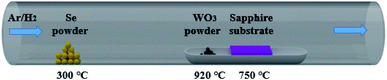 |
| | Fig. 1 Schematic of the experimental setup for CVD growth of the WSe2 atomic layers. | |
2.2 Experiments
WSe2 flakes were placed into the sample box with argon (Ar), then irradiated with γ-ray from a 60Co source. Irradiation was performed on a 60Co irradiator (22.57 GBq in total activity) at the Irradiation Center, China Institute of Atomic Energy, with a photon energy of 1.3 MeV. The irradiation doses were 0, 20, 40, 60, 80 and 100 kGy, respectively. The morphology of the as-synthesized samples was characterized by atomic force microscopy (AFM, Cypher S, Oxford Instruments, USA) and transmission electron microscopy (TEM, FEI-Themis Z, USA). Resolution scanning transmission electron microscopy (HRSTEM) was carried out using a high angle annular dark field (HAADF) detector. All of the STEM images presented in this manuscript were acquired in the HAADF mode. Photoluminescence (PL) and Raman spectra of the WSe2 sample were excited at room temperature using a Renishaw inVia micro-Raman spectrometer. Both PL spectra and Raman measurements were performed on the microscope using a laser of wavelength of 532 nm in an ambient environment at room temperature. The electrostatic properties of the sample were investigated by Kelvin probe force microscopy (KPFM). KPFM experiments were conducted under ambient conditions using Mikro-Masch CSC-17/Cr-Au tips with a force constant of 0.15 N m−1. In order to covert the contact potential difference (CPD) to the work function, the tips were calibrated with highly-ordered pyrolytic graphite (HOPG).
WSe2 monolayers were exfoliated from sapphire substrates, and transferred to the TEM grids with the following method. A PMMA solution (Mw = 950 K, 4 wt%, AR-P 679.04, Allresist) was spin-coated onto the source substrate at 3000 rpm for 1 min, and then baked at 100 °C for 30 min to form a thin film that encapsulated nanomaterials. A PMMA film was then peeled off in a KOH solution (1 M, 80 °C). The slight hydrolyzation of PMMA in the basic solution resulted in its peeling-off from the source substrate. Next, the PMMA film was attached to the micro copper grid (Gilder Grids, 200 mesh), and then annealed at 70 °C for 3 h. Finally, the PMMA film was removed by decomposing in acetone for 1 h, leaving the transferred nanomaterials anchored on the target substrate. We repeated it numerous times and used the annealing method to reduce mechanical or chemical damages during the transfer as much as possible.
2.3 Characterization
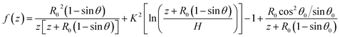
According to the Amonton's law, the friction force Ff is given by eqn (1):35where μ, FN, and Fadh are the friction coefficient, the normal force applied to probe, and the tip-sample adhesion force, respectively. Fadh is given by eqn (2):36where Fbg is a non-voltage-dependent background term, originating from, for example, capillary and van der Waals forces, and the Fe is the electrostatic force between the tip and sample.
Considering the CPD between the tip and sample, an effective sample bias is defined as eqn (3):37
where
Vs and
Vc are sample voltage and CPD. CPD can be expressed as
eqn (4):
38| | |
Vcpd = (Φtip − Φsample)/e
| (4) |
where
Φsample and
Φtip are the work functions of the sample and tip, respectively, and
e is the electronic charge. By modeling the tip as a spherical apex and cone,
Fe is given as
eqn (5)–(7):
39| | |
Fe = πε0[Vs + (Φsample − Φtip)/e]2f(z)
| (5) |
| |
 | (6) |
With
where
ε0,
Ve,
R0,
θ0 and
H are vacuum permittivity, effective sample bias, sphere radius of the tip, the apex half-angle of the tip, and effective tip height, respectively. The approximate expression of electrostatic force
f(
z) can be experimentally evaluated by tip geometric parameters.
DFT calculations were performed using the Vienna ab initio Simulation Package (VASP) with the projector augmented-wave method. Exchange and correlation effects were implemented using PBEsol, which is a Perdew–Burke–Ernzerhof generalized gradient approximation revised for solids. The energy cut-off for the plane-wave basis was set at 500 eV. For the first Brillouin zone, the Γ-center Monkhorst–Pack k-point mesh was chosen as 9 × 9 × 1. To separate the adjacent slabs, a 25 Å space vacuum was inserted in the direction that is normal to the monolayer. All the geometric structures were optimized until the maximum forces in all directions were less than 5 meV Å−1, and the convergence of the total energy became lower than 1 × 10⁻⁸ eV per atom.
3. Results and discussion
For high-performance devices, WSe2 flakes with uniform thicknesses and minimal roughness are essential.40 In particular, the WSe2 flake had a height of ∼0.70 nm (Fig. 2(a)), indicating a monolayer. Moreover, the AFM height profile confirms that most flakes are monolayers (Fig. 2(a)). The selected area electron diffraction (SAED) patterns are shown in Fig. 2(b). The hexagonally arranged diffraction spots can be indexed to the hexagonal symmetry of the [001] zone plane of the WSe2 lattice structures. Together, these studies (Fig. 2(a and b)) demonstrate the well-defined structure of the TMD monolayer WSe2 crystal with an atomically sharp interface. During the γ-ray irradiation in the Ar environment, high-energy photons facilitate the exoenergetic process, which generates selenium vacancies. A higher radiation dose is expected to create more selenium vacancies. Hence, we systematically studied the PL and Raman spectroscopy measurements on the WSe2 flake as a function of incrementally varied radiation doses (from 0, 20, 40, 60, 80 to 100 kGy). One peak at around 708 nm is observed on the high-energy regime (Fig. 2(c)), which has an equivalent energy of 1.75 eV and is identified as the neutral exciton X0. The position of X0 seems to be insensitive to the changing charge concentration41 and radiation dose. The higher peak at ∼709 nm is identified as an impurity trapped exciton.42 Robust peaks at ∼750 nm are attributed to the trion X−, which is a bounded three-particle state formed by a neutral exciton X0 and an excessive electron. The WSe2 crystals do not donate electrons to fill the gamma-induced positive charges (i.e., electron traps) on the substrate surface; hence, the PL peaks at 750 nm do not shift with the irradiation dose.34 This was made possible by the γ-ray irradiation that introduced anion (Se) vacancies, which rendered the sample effectively an n-doped WSe2 monolayer. The PL spectra suggest that the γ-ray irradiation treatment is an effective approach allowing the control of the structural defects in monolayers. In the absence of irradiation, a major peak at ∼250.6 cm−1 was identified as the in-plane vibrational mode E12g (Fig. 2(d)), accompanied by a small shoulder at ∼259 cm−1, which was identified as the out-of-plane vibrational mode A1g. As the radiation dose increases, the intensities of both E12g and A1g peaks are reduced. This reduction in intensity, however, is to a good approximation dependent linearly on the radiation dose. With the increase in the vacancy defect density, there are fewer W–Se bonds involved the E12g and A1g vibration modes, and thus, the restoring force constant of the corresponding peak continuously weakened.21 The broadening of FWHM also increases linearly as the radiation dose (Fig. 2(d)), which is most likely attributable to the lowered crystal quality caused by the treatment of high-energy photons.21 As the irradiation dose increases from 0 kGy to 100 kGy, we observed a blue-shift in the out-of-plane A1g mode, which is accompanied by a slight red-shift in the in-plane E12g mode (Fig. 2(d)). We attribute this Raman peak shift to the change in bond restoring force as a response to the vacancy.21,43 The stiffening of the out-of-plane A1g is much more prominent than the softening in-plane mode E12g, which showed the difference between the peak values of A1g and E12g as a function of the oxidation content. This feature is consistent with the Raman mode shift observed in MoS2, which is subjected to the electron irradiation treatment.43 We also estimated the selenium vacancy content corresponding to each proportion at different doses, which are 0/18, 1/32, 1/18, 2/18, 3/18, and 4/18, respectively. As one of the main results of this study, such a linear relationship between the changes in Raman modes and the oxidation content allowed us to engineer the monolayer properties at a quantitative level, which is highly desirable in device design and fabrication.
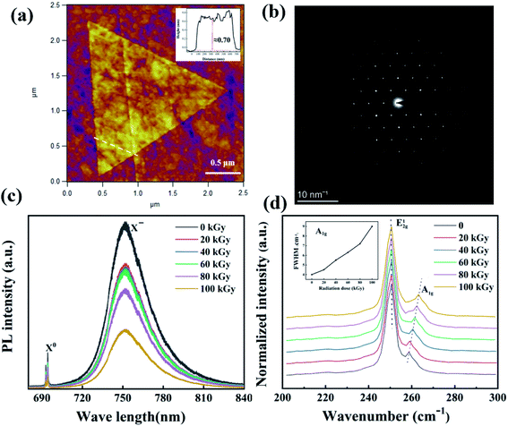 |
| | Fig. 2 (a) AFM image and height profile corresponding to a monolayer WSe2 flake. (b) Selected area electron diffraction (SEAD) patterns taken from monolayer WSe2. (c) PL spectra of monolayer WSe2 under different γ-ray oxidation contents (irradiation doses). Neutral exciton peak X0 is located at ∼708 nm and the trion X− peak is at ∼750 nm. (d) Raman spectra of monolayer WSe2 and γ-ray irradiation treated-WSe2 as a function of the irradiation dose. The subplot figure is the relationship between FWHM of A1g Raman band and radiation dose. | |
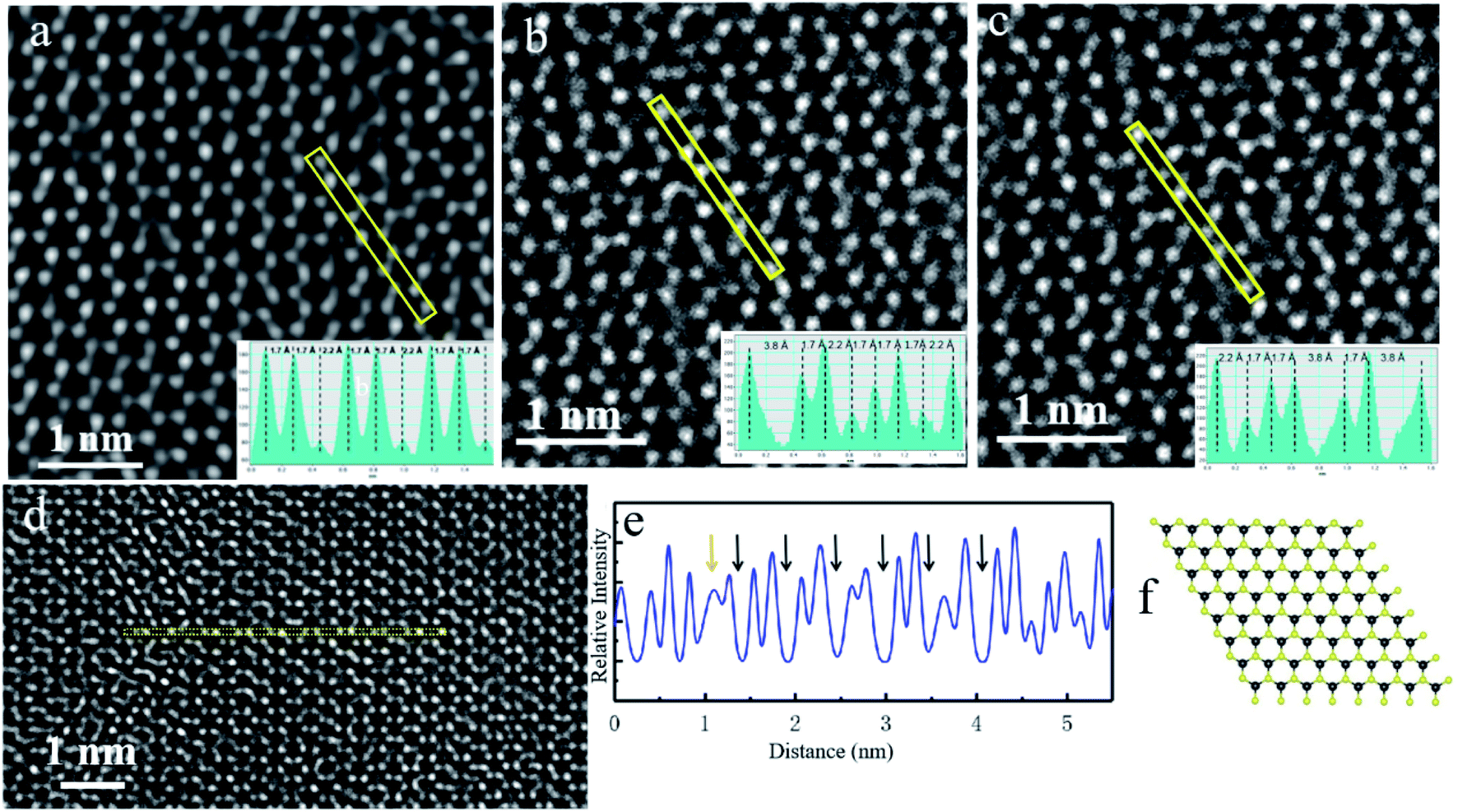
To further evaluate the crystallinity and determine the structure of the CVD-grown monolayer WSe2, we transferred the monolayer flakes to holey carbon grids for transmission electron microscopy (TEM) and scanning transmission electron microscopy (STEM) characterizations. Fig. 3(a) shows a high resolution HAADF-STEM experimental image obtained from the WSe2 sample. Scanning transmission electron microscopy (STEM) was employed to establish the correlation between the atomic arrangements. The contrast of the STEM high-angle annular dark-field (STEM-HAADF) image is sensitive to the atomic number, which makes it possible to identify the detailed atomic arrangement.44 In Fig. 3(a), one-single layer (Se–W–Se) hexagonal lattice is observed. As it can be observed that two different atomic columns can be noticed in the image, the most intense corresponding to W atoms (Z = 74), and the less intense to Se atoms (Z = 34). This is due to the large difference in the atomic number of both elements (W = 74 and Se = 34).45 The interatomic distances between the atoms in the selected region are 1.7, 1.7 and 2.2 Å, repeatedly. This indicates the coexistence of W and Se atoms, and that these atoms are arranged regularly. The interatomic distances between the atoms in the selected region are 3.8, 1.7, 2.2, 1.7, 1.7, 1.7 Å (Fig. 3(b)). 3.8 Å indicates one vacancy site in the pristine WSe2 crystal. With the increasing of vacancy content induced by irradiation, more vacancy site took place (Fig. 3(c)), making the atom arrangement more irregular, which caused the complexity of the crystal structure to increase. Fig. 3(b–d) demonstrate the growing asymmetric of the WSe2 crystal and gradual increase in the disorder in the lattice due to the creation of vacancy defect sites. In particular, as shown in Fig. 3(d and e), the black arrows (interatomic distance ∼ 3.8 Å) indicate vacancy sites and the yellow arrow indicates that other impurities may be introduced. Thus, irradiation caused the crystal internal structure change from quantitative to qualitative. These results may be able to provide some explanation for the decrease in the intensities of E12g and A1g peaks and the broadening of FWHM linearly as the radiation increased. The vertical view of the pristine monolayer WSe2 atomic arrangement is shown in Fig. 4(f). The same atoms are in lines. This configuration assists us to compare Fig. 4(a–d).
 |
| | Fig. 3 Atomic-resolution HAADF-STEM image of monolayer WSe2, the corresponding intensity profile (the lower right) with radiation doses of (a) 0 kGy, (b) 20 kGy (c) 40 kGy and (d) 60 kGy, respectively. (e) The corresponding intensity profile of the yellow selected area of (d). (f) The vertical view of the defect-free monolayer WSe2 atomic arrangement. The black ball represents the W atom, the yellow ball represents Se atom. | |
The band structure presented in Fig. 4 shows that the bandgap of WSe2 decreases monotonically from 2.10 eV to 0.79 eV, as the rate of selenium vacancy increases from 0% to 4/18. This results in a red-shift of the PL peaks upon γ-ray irradiation. The increase in vacancy also slightly raises the position of the valence band at Γ and the conduction band minimum (CBM) at the K space. Moreover, the bandgap is found to become indirect at a high vacancy rate, leading to the decrease in the PL intensity after the γ-ray irradiation. Therefore, the radiative recombination should be assisted by electron–phonon scattering in the first Brillouin zone, which contributes to the substantial reduction of the PL intensity. The work function (Φsample) of each vacancy rate was also calculated by DFT.
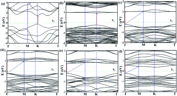 |
| | Fig. 4 Band structure calculated using DFT for monolayer WSe2. (a) Energy bands of pristine, (b) band structure of monolayer WSe2 with thirty-two Se atoms replaced by one, and (c–f) band structure of monolayer WSe2 with eighteen Se atoms replaced by one, two, three and four Se vacancies, respectively. | |
The friction force versus normal load and the friction coefficient versus radiation dose are shown in Fig. 5(a and b). Clearly, the friction force and friction coefficient increased monotonically with the increase in the radiation dose. This is different from the previous report because γ-irradiation causes the molecular impact movement in the sample chamber, which increases the number of cavities, yields a high density of selenium vacancies,34 generates deep electron traps,46 which can invoke as charged scattering centers, making uneven stress distribution of the surfaces. Fig. 5(c) shows that in a dry environment, removing the influence of adhesion, the main factor of friction increase is caused by irradiation. Fig. 5(d) shows that the surface potential difference first decreases and then increases with the irradiation, and the irradiation regulates the distribution of the surface potential. The principle is explained by the subsequent DFT theory. The electrostatic principle is commonly applied in MEMS sensors and divers,47 so that the friction parts and moving modules are related to the friction and wear problems under electromechanical coupling effects. We also perform first-principles calculations to determine the band structure at different defect concentrations. The values of the electrostatic force and the CPD are not constant with radiation dose (Fig. 5(e and f)), implying a strong correlation with the amount of vacancy defect introduced by irradiation. Such a nonlinear dependence is consistent with the electrostatic force and the CPD calculated using DFT. The CPD obtained from calculation shows a similar trend to that of obtained from KPFM measurements. This indicates that the variation of work functions (Φsample) originated from the change in the band structure, and the defects introduced in lattice by irradiation. The difference between the Fermi level and the vacuum level determined the variation of work functions. Therefore, the change of the work function is caused by the variation of density of states near the Fermi level.48,49 The experimental results can be explained by that the vacancy position is related to the Se vacancy concentration. The work function has been found to strongly correlate with the Se vacancy site. Se vacancy at the edge site is dominant for the defect-free WSe2 lattice, while vacancy at the in-plane site occurs for vacancy-rich WSe2 nanosheets.50 When the vacancy concentration is low, the influence position of increasing work function is greater than that of the decreasing work function, so the work function increases. On the contrary, when the vacancy concentration is high, the influence position of decreasing work function is greater than that of the increasing work function, so the work function decreases. Thereby, the trends of the electrostatic force and CPD changed accordingly. This opens a new venue to process WSe2 monolayers towards numerous industrial applications.
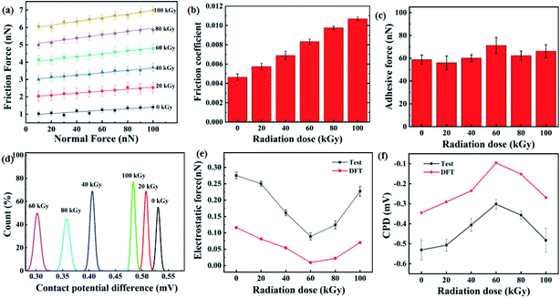 |
| | Fig. 5 (a) The friction force vs. normal load, (b and c) the friction coefficient and the adhesive force vs. the radiation dose, (d) contact potential distributions and CPD test values under different radiation dose from 0 to 100 kGy. Different colors correspond to measurements performed under different radiation doses, (e) the test results (black lines) and DFT (red lines) of the electrostatic force vs. the radiation dose, and (f) the test results (black lines) and DFT (red lines) of the CPD vs. the radiation dose. | |
4. Conclusions
Our study shows a new defect-inducing technique to engineer the bandgap and control the optical, frictional and electrostatic properties of atomically thin WSe2. In summary, the WSe2 monolayer behaves as an n-doped semiconductor, in which the carrier concentration increases with the radiation dose. The measured friction was found to monotonically increase with the irradiation dose. The surface potential was also altered by the introduction of the vacancy defect. First principles calculations reveal that the WSe2 monolayer undergoes a transition from a direct-gap semiconductor to an indirect one with the generation of vacancy defects. The manipulation of the electrostatic force, work function and contact potential as functions of the vacancy defect content opens a new venue to engineer transition metal dichalcogenides via γ-ray irradiation.
Conflicts of interest
There is no conflict of interest.
Acknowledgements
This work was supported by the National Natural Science Foundation of China (11832016, 51775471), Changsha Zhuzhou Xiangtan Landmark Engineering Technology Project (2020GK2014, 2019XK2303), and Xiangtan Science and Technology Project (ZDZD20191007), the Hunan Innovative Province Construction Special Major Landmark Innovation Demonstration Project (2019XK2303), and Xiangtan University Graduate Research and Innovation 20 Project (XDCX2020B127).
References
- J. A. Wilson and A. D. Yoffe, Adv. Phys., 1969, 18, 193–335 CrossRef CAS.
- Q. H. Wang, K. Kalantarzadeh, A. Kis, J. N. Coleman and M. S. Strano, Nat. Nanotechnol., 2012, 7, 699–712 CrossRef CAS.
- D. Xiao, G. B. Liu, W. X. Feng, X. D. Xu and W. Yao, Phys. Rev. Lett., 2012, 108, 196802 CrossRef PubMed.
- A. Kuc, N. Zibouche and T. Heine, Phys. Rev. B: Condens. Matter Mater. Phys., 2011, 83, 245213 CrossRef.
- K. F. Mak, C. Lee, J. Hone, J. Shan and T. F. Heinz, Phys. Rev. Lett., 2010, 105, 136805 CrossRef PubMed.
- A. Splendiani, L. Sun, Y. Zhang, T. Li, J. Kim, C.-Y. Chim, G. Galli and F. Wang, Nano Lett., 2010, 10, 1271–1275 CrossRef CAS.
- G. Eda, H. Yamaguchi, D. Voiry, T. Fujita, M. Chen and M. Chhowalla, Nano Lett., 2011, 11, 5111–5116 CrossRef CAS PubMed.
- W. Zhao, Z. Ghorannevis, L. Chu, M. Toh, C. Kloc, P. H. Tan and G. Eda, ACS Nano, 2013, 7, 791–797 CrossRef CAS PubMed.
- K. F. Mak, K. He, C. Lee, G. H. Lee, J. Hone, T. F. Heinz and J. Shan, Nat. Mater., 2012, 12, 207–211 CrossRef PubMed.
- K. He, N. Kumar, L. Zhao, Z. Wang, K. F. Mak, H. Zhao and J. Shan, Phys. Rev. Lett., 2014, 113, 026803 CrossRef CAS.
- Z. Ye, T. Cao, K. O. Brien, H. Zhu, X. Yin, Y. Wang, S. G. Louie and X. Zhang, Nature, 2014, 513, 214 CrossRef CAS PubMed.
- A. T. Hanbicki, M. Currie, G. Kioseoglou, A. L. Friedman and B. T. Jonker, Solid State Commun., 2015, 203, 16–20 CrossRef CAS.
- J. Huang, T. B. Hoang and M. H. Mikkelsen, Sci. Rep., 2016, 6, 22414 CrossRef CAS.
- K. F. Mak and J. Shan, Nat. Photonics, 2016, 10, 216–226 CrossRef CAS.
- C. Li, Q. Cao, F. Wang, Y. Xiao, Y. Li, J. J. Delaunay and H. Zhu, Chem. Soc. Rev., 2018, 47, 4981–5037 RSC.
- Z. Y. Zhu, Y. C. Cheng and U. Schwingenschlögl, Phys. Rev. B: Condens. Matter Mater. Phys., 2011, 84, 153402 CrossRef.
- K. Hao, G. Moody, F. Wu, C. K. Dass, L. Xu, C. H. Chen, M. Y. Li, L. J. Li, A. H. MacDonald and X. Li, Nat. Phys., 2016, 12, 677 Search PubMed.
- H. Schmidt, F. Giustiniano and G. Eda, Chem. Soc. Rev., 2015, 44, 7715–7736 RSC.
- H. Nan, Z. Wang, W. Wang, Z. Liang, Y. Lu, Q. Chen, D. He, P. Tan, F. Miao, X. Wang, J. Wang and Z. Ni, ACS Nano, 2014, 8, 5738–5745 CrossRef CAS PubMed.
- J. Lu, A. Carvalho, X.
K. Chan, H. Liu, B. Liu, E. S. Tok, K. P. Loh, A. H. C. Neto and C. H. Sow, Nano Lett., 2015, 15, 3524–3532 CrossRef CAS PubMed.
- Z. T. Wu and Z. H. Ni, Nanophotonics, 2017, 6, 1219–1237 CAS.
- G. R. Bhimanapati, M. Wetherington, S. Mahabir and J. A. Robinson, 2D Mater., 2016, 3, 025028 CrossRef.
- M. Foxe, G. Lopez, I. Childres, R. Jalilian, C. Roecker, J. Boguski, I. Jovanovic and Y. P. Chen, IEEE Nucl. Sci. Symp. Conf. Rec., 2009, 90–95 CAS.
- M. R. Islam, N. Kang, U. Bhanu, H. P. Paudel, M. Erementchouk, L. Tetard, M. N. Leuenberger and S. I. Khondaker, Nanoscale, 2014, 6, 10033–10039 RSC.
- J. Yang, S. Kim, W. Choi, S. H. Park, Y. Jung, M. H. Cho and H. Kim, ACS Appl. Mater. Interfaces, 2013, 5, 4739–4744 CrossRef CAS PubMed.
- H. Conley, B. Wang, J. I. Ziegler, J. R. F. Haglund, S. T. Pantelides and K. I. Bolotin, Nano Lett., 2013, 13, 3626–3630 CrossRef CAS.
- Y. L. Liu, H. Y. Nan, X. Wu, W. Pan, W. Wang, J. Bai, W. Zhao, L. Sun, X. Wang and Z. Ni, ACS Nano, 2013, 7, 4202–4209 CrossRef CAS PubMed.
- E. D. Corro, H. Terrones, A. Elias, C. Fantini, S. Feng, M. A. Nguyen, T. E. Mallouk, M. Terrones and M. A. Pimenta, ACS Nano, 2014, 8, 9629–9635 CrossRef.
- M. X. Han, Z. Y. Ji, L. W. Shang, Y. P. Chen, H. Wang, X. Liu, D. M. Li and M. Liu, Chin. Phys. B, 2011, 20, 086102 CrossRef.
- Y. Wang, Y. Feng, F. Mo, G. Qian, Y. Chen, D. Yu, Y. Wang and X. Zhang, Appl. Phys. Lett., 2014, 105, 023102 CrossRef.
- R. C. Walker II, T. Shi, E. C. Silva, I. Jovanovic and J. A. Robinson, Phys. Status Solidi A, 2016, 213, 3065–3077 CrossRef.
- B. Du, Y. Gao and Z. Huo, J. Electrost., 2009, 67, 22–26 CrossRef CAS.
- T. Vogl, K. Sripathy, A. Sharma, P. Reddy, J. Sullivan, J. R. Machacek, L. Zhang, F. Karouta, B. C. Buchler, M. W. Doherty, Y. Lu and P. K. Lam, Nat. Commun., 2019, 10, 1202 CrossRef.
- S. Elafandi, R. Christiansen, N. Azam, M. Cichon, M. Park, M. C. Hamilton and M. Mahjouri-Samani, Appl. Phys. Lett., 2020, 116, 213105 CrossRef CAS.
- E. Riedo, F. Lévy and H. Brune, Phys. Rev. Lett., 2002, 88, 185505 CrossRef PubMed.
- B. M. Law and F. Rieutord, Phys. Rev. B: Condens. Matter Mater. Phys., 2002, 66, 035402 CrossRef.
- S. Hudlet, M. Saint Jean, C. Guthmann and J. Berger, Eur. Phys. J. B, 1998, 2, 5–10 CrossRef CAS.
- Y. Qi, J. Y. Park, B. L. M. Hendriksen, D. F. Ogletree and M. Salmeron, Phys. Rev. B: Condens. Matter Mater. Phys., 2008, 77, 184105 CrossRef.
- W. Melitz, J. Shen, A. C. Kummel and S. Lee, Surf. Sci. Rep., 2011, 66, 1–27 CrossRef CAS.
- H. Fang, S. Chuang, T. C. Chang, K. Takei, T. Takahashi and A. Javey, Nano Lett., 2012, 12, 3788–3792 CrossRef CAS PubMed.
- A. M. Jones, H. Yu, N. J. Ghimire, S. Wu, G. Aivazian, J. S. Ross, B. Zhao, J. Yan, D. G. Mandrus, D. Xiao, W. Yao and X. Xu, Nat. Nanotechnol., 2013, 8, 634–638 CrossRef CAS PubMed.
- J. S. Ross, S. Wu, H. Yu, N. J. Ghimire, A. M. Jones, G. Aivazian, J. Yan, D. G. Mandrus, D. Xiao, W. Yao and X. Xu, Nat. Commun., 2013, 4, 1474 CrossRef PubMed.
- W. M. Parkin, A. Balan, L. Liang, P. M. Das, M. Lamparski, C. H. Naylor, J. A. Rodríguez-Manzo, A. T. C. Johnson, V. Meunier and M. Drndíc, ACS Nano, 2016, 10, 4134–4142 CrossRef CAS PubMed.
- M. Xia, B. Li and K. Yin, ACS Nano, 2015, 9(12), 12246–12254 CrossRef CAS PubMed.
- A. Garcia, et al., Ultramicroscopy, 2014, 146, 33–38 CrossRef CAS PubMed.
- T. Vogl, K. Sripathy, A. Sharma, P. Reddy, J. Sullivan, J. R. Machacek, L. Zhang, F. Karouta, B. C. Buchler, M. W. Doherty, Y. Lu and P. K. Lam, Nat. Commun., 2019, 10(1), 1202 CrossRef PubMed.
- W. C. Chuang, H. L. Lee, P. Z. Chang and Y. C. Hu, Sensors, 2010, 10, 6149–6171 CrossRef PubMed.
- Y.-J. Yu, Y. Zhao, S. Ryu, L. E. Brus, K. S. Kim and P. Kim, Nano Lett., 2009, 9, 3430 CrossRef CAS PubMed.
- B. Kang, S. Lim, W. H. Lee, S. B. Jo and K. Cho, Adv. Mater., 2013, 25, 5856 CrossRef CAS PubMed.
- J. Hu, L. Yu and J. Deng, et al., Nat. Catal., 2021, 4, 242–250 CrossRef.
|
| This journal is © The Royal Society of Chemistry 2021 |
Click here to see how this site uses Cookies. View our privacy policy here. 
 Open Access Article
 This Open Access Article is licensed under a Creative Commons Attribution-Non Commercial 3.0 Unported Licence
 *ab,
Xuejun Zheng
*ab,
Xuejun Zheng