
 Open Access Article
 This Open Access Article is licensed under a Creative Commons Attribution-Non Commercial 3.0 Unported Licence
Enhanced negative magnetoresistance near the charge neutral point in Cr doped topological insulator†
Qixun Guoa,
Yu Wuab,
Dongwei Wangc,
Gang Hand,
Xuemin Wangd,
Libo Fue,
Lihua Wang e,
Wei Hef,
Tao Zhuf,
Zhendong Zhug,
Tao Liuh,
Guanghua Yua and
Jiao Teng*a
e,
Wei Hef,
Tao Zhuf,
Zhendong Zhug,
Tao Liuh,
Guanghua Yua and
Jiao Teng*a
aDepartment of Material Physics and Chemistry, University of Science and Technology Beijing, Beijing 100083, P. R. China. E-mail: tengjiao@mater.ustb.edu.cn
bBeijing Tongfang Huachuang Technology Co., Ltd, Beijing 100089, P. R. China
cCAS Key Laboratory of Standardization and Measurement for Nanotechnology, National Center for Nanoscience and Technology, Beijing 100190, P. R. China
dCollaborative Innovation Center of Advanced Steel Technology, University of Science and Technology Beijing, Beijing 100083, P. R. China
eInstitute of Microstructure and Property of Advanced Materials, Beijing Key Lab of Microstructure and Property of Advanced Materials, Beijing University of Technology, Beijing 100124, P. R. China
fBeijing National Laboratory for Condensed Matter Physics and Institute of Physics, Chinese Academy of Sciences, Beijing 100190, P. R. China
gNational Institute of Metrology, Beijing 100029, P. R. China
hNational Engineering Research Center of Electromagnetic Radiation Control Materials, University of Electronic Science and Technology of China, Chengdu 610054, P. R. China
First published on 14th April 2021
Abstract
Negative magnetoresistance (MR) is not only of great fundamental interest for condensed matter physics and materials science, but also important for practical applications, especially magnetic data storage and sensors. However, the microscopic origin of negative MR is still elusive and the nature of the negative MR in magnetic topological insulators has still not been completely elucidated. Here, we report magnetotransport studies on Cr doped (Bi1−xSbx)2Te3 topological insulator thin films grown by magnetron sputtering. At the temperature of 2 K, a giant negative MR reaching 61% is observed at H = 2 T. We show that the negative MR is closely related to the position of the Fermi level, and it reaches the maximum when the Fermi level is gated near the charge neutral point. We attribute these results to the Coulomb potential due to the random composition fluctuations in Cr doped (Bi1−xSbx)2Te3. Our results provide a deeper insight into the mechanism of negative MR, and are helpful to realize the quantum anomalous Hall effect in the sputtered Cr-(Bi1−xSbx)2Te3 thin-film systems by tuning the Fermi level and reducing disorder effects.
Introduction
Topological insulators (TIs) are a new state of quantum matter with unique spin and charge properties owing to the nontrivial band topology and their interesting Dirac surface state properties.1,2 By tuning the Fermi level close to the charge neutral point, various unique quantum phenomena of TIs have been discovered both experimentally and theoretically, leading to a fascinating prospect in the field of TIs. For instance, the quantum anomalous Hall effect (QAHE), an exotic quantum phenomenon originating from dissipationless chiral channels, was achieved in Cr-doped (Bi1−xSbx)2Te3 thin films in the past seven years.3–11 In recent years, non-saturating linear magnetoresistance has been found to be most pronounced when the Fermi level is electrically tuned near the charge neutral point.12–14 Wu and colleagues reported that the spin–orbit torque from the Dirac surface state is significantly enhanced near the charge neutral point in (Bi1−xSbx)2Te3.15 Besides, as the Fermi level is systematically tuned in (Bi1−xSbx)2Te3 thin films with a fixed thickness via varying Bi concentration x, an enhanced, tunable spin Seebeck effect16 and spin dynamics17 can be observed in the (Bi1−xSbx)2Te3/YIG heterostructures when the Fermi level approaches the charge neutral point.Because (Bi1−xSbx)2Te3 is an alloy with random compositional inhomogeneities, disorders occur naturally. The randomly distributed ions give rise to the fluctuations in the charge distribution and Coulomb potential associated with these charges. Due to the vanishing number of free charge carriers near complete compensation, these fluctuations are poorly screened and can locally bend the valence and conduction band edges. These fluctuations are strong enough that the valence or conduction band edge is bent above or below the Fermi level, yielding local accumulations of charge carriers, the so-called puddles.18 The existence of charge puddles has been confirmed by various methods such as scanning tunneling microscopy/spectroscopy (STM/STS),18–20 optical conductivity21 and transport measurements.13,22–24 Even though a lot of works have been carried out to clarify the influence of charge puddles on the electron transport properties of (Bi1−xSbx)2Te3 thin films, the effects of charge puddles on the magnetotransport properties of disordered magnetic topological insulator are rarely studied.
In this work, the magnetotransport properties of Cr-doped (Bi1−xSbx)2Te3 thin films synthesized by magnetron sputtering with thickness around 8 nm were measured through back gate modulation at low temperatures. Electron and hole puddles are formed in these thin films at low temperature, and a variable range hopping (VRH)-like behavior is observed. By varying Sb concentration x and systematically tuning the chemical potential, we find that the negative magnetoresistance (MR) strongly depends on the Fermi level position and reaches the maximum near the charge neutral point, indicating dominating magnetotransport properties from charge puddles.
Method
The Cry(Bi1−xSbx)2−yTe3 (CBST) thin films were deposited on silicon (100) substrates (300 nm SiO2 /silicon) by a magnetron sputtering system (ATC-1800F). The CBST thin films were deposited from Bi2Te3 (99.99%), Sb2Te3 (99.99%) and Cr (99.95%) targets by dc sputtering and a Te (99.99%) target by rf sputtering. The base pressure of the deposition chamber was below 3 × 10⁻⁷ Torr, and the working argon pressure was set at 2 × 10⁻³ Torr. During deposition, the Si/SiO2 substrate was kept at 175 °C for CBST thin films. After deposition, the thin films were annealed in situ at the same temperature for 25 min as the deposition. We prepared three samples, CBST1, CBST2, and CBST3 with the same doping concentration of y = 0.24 and the same thickness of 8 nm. To control the film composition and carrier type, the sputtering power of the Sb2Te3 target was fixed at 30 W while the sputtering power of the Bi2Te3 target was 15.0 W, 16.5 W, and 17.5 W for CBST1, CBST2, and CBST3, respectively. The nominal Sb concentrations x are 0.64, 0.62 and 0.6 for CBST1, CBST2, and CBST3, respectively. The Sb, Bi and Cr concentrations in the films were determined by their sputtering power ratios and inductively coupled plasma atomic emission spectroscopy (ICP-AES). CBST2 and CBST3 were capped in situ with a 4 nm thick Al thin film, which naturally oxidized upon exposure to atmosphere. CBST1 was uncapped. The transport measurements are carried out using a 9 T Physical Properties Measurement System (PPMS, Quantum Design) with a base temperature of 2 K. Thin films of CBST were transferred onto holey carbon support film for TEM characterizations, which were performed with a Titan-ETEM operating at 300 kV.Results
The carrier type of Sb2Te3 is naturally p-type, while Bi2Te3 is n-type. The sputtering powers of Sb2Te3, and Bi2Te3 targets are carefully controlled to maintain magnetic topological insulator thin films with required carrier type. It is reported that both Sb2Te3 and Bi2Te3 have the same crystal structure and close lattice constants, making it ideal to form (Bi1−xSbx)2Te3 ternary compounds with arbitrary mixing ratio.25 Transmission electron microscopy (TEM) was used to examine the structure of the CBST2 thin films (Fig. S1†).Fig. 1(a) and (b) show the magnetic field dependence of Hall resistance and MR with the magnetic field applied perpendicular to the film plane of CBST1, CBST2, and CBST3 at T = 2 K, respectively. The nearly square-shaped Hall hysteresis loops and butterfly-shaped MR curves suggest that the long-range ferromagnetic order with perpendicular magnetic anisotropy is developed at T = 2 K. Generally, the total Hall resistance is expressed as Rxy = RHH + RAHE(M),26,27 where RH is the slope of the ordinary Hall background, H is the applied magnetic field, RAHE is the anomalous Hall resistance, and M is the magnetization component in the perpendicular direction. It can be seen that in Fig. 1(a) with decreasing Sb content x (from CBST1 to CBST3), the slope of ordinary Hall background at high field evolves from positive to negative, indicating the change of the dominating carriers from p- to n-type at around x = 0.62 (CBST2). On the other hand, among these samples, anomalous Hall resistance RAHE shows the largest value of 13.2 kΩ for CBST2, reaching 1/2 of the quantum anomalous Hall resistance (h/e2 ≈ 25.8 kΩ). As shown in the inset of Fig. 1(a), the coercive field Hc of the p-type CBST1 is much larger than that of CBST2 and CBST3, which is consistent with previous reports,28,29 indicating a hole-mediated Ruderman–Kittel–Kasuya–Yosida (RKKY) coupling signature. The MR is defined as ΔRxx/Rxx(0) = [Rxx(H) − Rxx(0)]/Rxx(0) × 100%, where Rxx(0) and Rxx(H) are the resistances at zero field and at an applied field H, respectively. Interestingly, the values of MR are nearly proportional to the Hall resistance, and a giant negative MR of −60% at 2 T magnetic field is observed in CBST2 sample, exceeding by far the MR effects from devices capable for realizing the QAHE.3
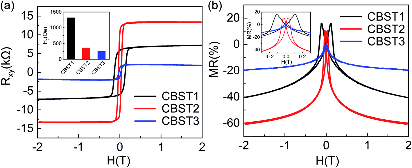 | ||
| Fig. 1 Magnetic field dependence of the hall resistance (Rxy) (a) and longitudinal sheet resistance Rxx (in terms of MR) (b) for CBST1, CBST2 and CBST3 at T = 2 K. The inset of (a) shows the coercive field Hc of CBST1, CBST2, and CBST3. The inset of (b) shows a zoomed-in view of MR-H with −0.3 T < H < 0.3 T. | ||
To understand the behavior and the underlying mechanisms of the giant negative MR, we tune the position of Fermi level of the material by applying different voltages to back gate (Fig. 2(a)). Fig. 2(b) and (c) show the Hall hysteresis loops and MR curves of the sample CBST2 at different gate voltages. It can be seen that both Rxy and MR can be effectively tuned by back gate voltages. At different gate voltages, we extract the ordinary Hall coefficients RH and anomalous Hall resistance RAHE from the slope of Hall curves and the intercept of the linear background at a high magnetic field, respectively. A schematic of gate voltage dependence of the RH is shown in each inset of Fig. 2(d)–(f).12,23,30 With the maximum and minimum points on the curve, three distinguished zones were formed and labeled with I, II and III. The positive RH increases until it reaches a maximum in region I, indicating the hole-dominated transport. In region II, the RH decreases monotonously from the positive maximum to the negative minimum. In region III, the negative RH increases with back gate, indicating the electron-dominated transport. The carrier densities can be calculated by p2D = 1/(eRH) with p2D the density of hole type carriers in region I and n2D = 1/(eRH) with n2D the density of electrons in region III. However, in the region II, assuming only a single carrier type of density 1/(eRH) would result in an infinite carrier density at RH = 0, which is unphysical. This can only be explained by a two-carrier-type model in which electrons and holes coexist and give rise to the formation of charge puddles. The gate voltage at the zero RH is charge neutral point (CNP) voltage (VCNP), where the electrons and holes have the exactly same density.23
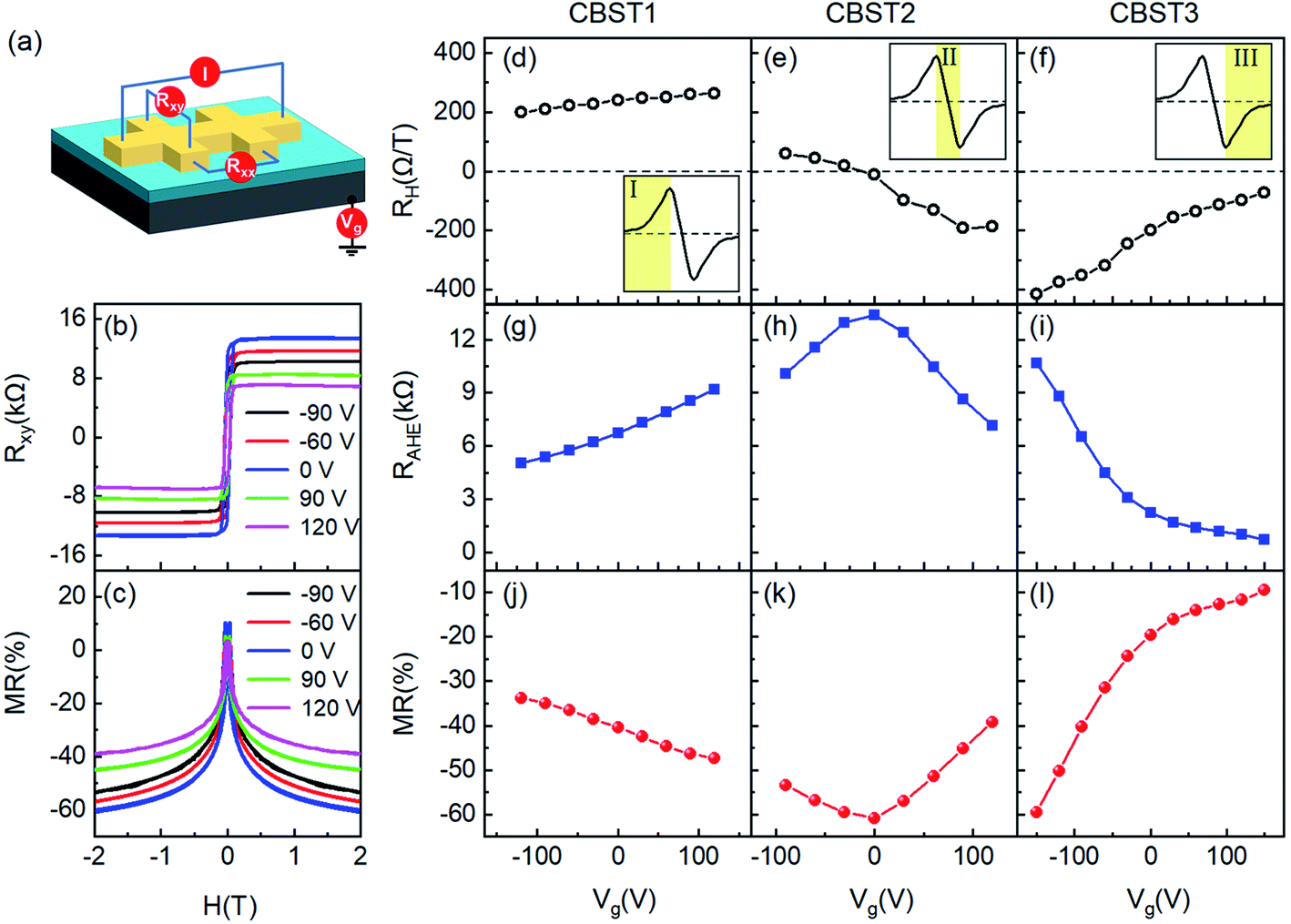 | ||
| Fig. 2 (a) The schematic illustration of hall bar device using SiO2 as the back-gate dielectric. (a) Hall bar geometry is used to measure the Rxx and Rxy simultaneously under various gate voltages Vg and magnetic field. (b) Hall resistance Rxy and (c) MR vs. H at different gate voltages of the sample CBST2 at a temperature of 2 K. (d–l) Gate voltage dependence of RH, RAHE and MR at 2 T for p-type CBST1 (d, g and j), near compensated CBST2 (e, h and k) and n-type CBST3 (f, i and l) magnetic topological insulator samples. The insets of (d–f) are schematic of gate voltage dependence of the hall coefficient RH. The area shaded in yellow and labeled I, II and III in each inset of (d–f) represents three different transport regimes: hole-doped, electron–hole puddles and electron-doped, respectively. | ||
In our Si/SiO2/Cr(Bi,Sb)2Te3 system, it is hard to observe the three regions in one sample. However, the above three CBST samples just can cover the whole region: CBST1, CBST2 and CBST3 are in region I, II and III (Fig. 2(d)–(f)), respectively. In Fig. 2(g), the value of the RAHE increases with increasing Vg for the CBST1 sample. For the near compensated CBST2 sample (Fig. 2(h)), we can see that the RAHE increases as Vg increases from −90 V to 0 V, reaches a peak at 0 V (just the VCNP of this sample), and then decreases with increasing Vg. RAHE decreases with increasing Vg for the n-type CBST3 sample (Fig. 2(i)). Even more interestingly, the trends of MR–Vg curves are just opposite to the RAHE–Vg: the maximum values of RAHE and MR happen near the charge neutral point, and gradually decrease on both sides of the charge neutral point. We already know that RAHE has a maximum value near the charge neutral point, even reaching QAHE, but what is the mechanism of giant MR near the charge neutral point is still unclear.
To gain a deeper understanding of the mechanisms of the giant negative MR, we also measured the temperature dependence of MR and Rxx of Cr doped topological insulators, as shown in Fig. 3(a)–(d). For CBST1 and CBST2, the MR is always negative below 20 K, while for CBST3 the evolution of MR with decreasing temperature shows a crossover from positive to negative at T = 8 K (Fig. 3(a)). It should be noted that, at the Curie temperature Tc of each sample the sign of MR has not changed. Besides, although the Tc of CBST3 is close to and even higher than that of CBST2, the temperature dependence of MR of CBST3 is significantly different from that of CBST2, and the value of MR is much smaller than CBST2. The difference between Tc and the crossover temperature at which the sign of MR changes indicate that the ferromagnetic transition cannot account for the giant MR at low temperatures. On the other hand, we notice that at low temperatures, the degree of disorders of these samples is different. The sheet resistances show insulating behavior over the whole temperature range (Fig. 3(b)–(d)), indicating the Fermi level EF is within the bulk band gap. In the high temperature regime Rxx increases slowly the decreases of T, while in the low temperature regime Rxx exhibits a rapidly increase. We estimate the disorder level by taking the dimensionless conductivity, g = kFl= (h/e2)/Rxx, where kF is the Fermi wave vector and l is the mean free path. According to the Ioffe–Regel criterion,31 kFl ≫ 1 indicates a weak disorder system, whereas kFl ≪ 1 indicates a strong disorder system. The Rxx–T curves of CBST1 and CBST2 show a transition from weak disorder to strong disorder when temperature decreases from 300 to 2 K. However, the disorder level of CBST3 is much lower than that of CBST1 and CBST2. These results strongly suggest that the mechanism of the negative MR in Cr doped topological insulator thin films is related to disorder effect: in the weak disorder case, the MR maintains positive, while with increasing disorder, the MR changes from positive to negative.
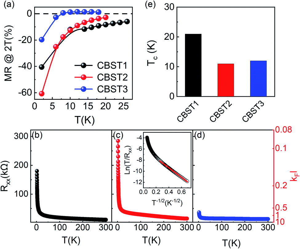 | ||
| Fig. 3 (a) The temperature dependence of MR values of CBST thin films at H = 2 T. Sheet resistance (Rxx) vs. temperature curve for CBST1 (b), CBST2 (c), and CBST3 (d), respectively. The inset shows the semi-logarithmic-scale plot of ln(T/Rxx) vs. T−1/2. The red straight line is the fitting of the VRH behavior to the data at low temperature. (e) The curie temperatures Tc for CBST1, CBST2 and CBST3 samples are 21, 11 and 12 K, respectively. | ||
Furthermore, we find that at low temperature the resistance can be well described by the variable range hopping (VRH) conduction process. In general, the hopping transport can be characterized as R(T) = R0T![[thin space (1/6-em)]](https://www.rsc.org/images/entities/char_2009.gif) exp[(T0/T)p], where R0 is a prefactor, T0 is a characteristic temperature, and p is the exponent depending on the details of density of states around Fermi level. For Mott-VRH,31 the density of states is constant, leading to p = 1/(d + 1) for materials with effective dimension d, whereas for Efros–Shklovskii (ES)32,33 VRH, which considers Coulomb interactions, the density of states vanishes at the Fermi level, leading to p = 1/2 regardless of the dimensionality. Our results support ES hopping rather than Mott hopping behavior. Inset of Fig. 3(c) shows that at low temperatures, ln(T/Rxx) has a linear dependence on T−1/2. These results provide evidence of the existence of electron–hole Coulomb interactions in our disordered magnetic topological insulator. Fig. 4 shows the schematic of the spatial electronic structure of the CBST film, which is highly inhomogeneous and is broken into electron and hole puddles at low temperature.
exp[(T0/T)p], where R0 is a prefactor, T0 is a characteristic temperature, and p is the exponent depending on the details of density of states around Fermi level. For Mott-VRH,31 the density of states is constant, leading to p = 1/(d + 1) for materials with effective dimension d, whereas for Efros–Shklovskii (ES)32,33 VRH, which considers Coulomb interactions, the density of states vanishes at the Fermi level, leading to p = 1/2 regardless of the dimensionality. Our results support ES hopping rather than Mott hopping behavior. Inset of Fig. 3(c) shows that at low temperatures, ln(T/Rxx) has a linear dependence on T−1/2. These results provide evidence of the existence of electron–hole Coulomb interactions in our disordered magnetic topological insulator. Fig. 4 shows the schematic of the spatial electronic structure of the CBST film, which is highly inhomogeneous and is broken into electron and hole puddles at low temperature.
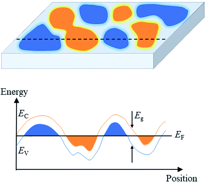 | ||
| Fig. 4 Cartoon illustration of charge puddles in the topological insulator thin films with strong fluctuations due to the compensation doping. The blue and orange filled areas denote nanoscale hole and electron puddles, respectively. The lower panel is the cross section along the broken black line drawn in the upper panel. The solid black line shows the Fermi level. | ||
Discussion
It has been shown in this study that a giant negative MR of −60% is observed at the charge neutral point and a strong correlation between the negative MR and the disorder effect in the magnetic doped topological insulators exists. We have also confirmed that the disorder effect in low temperatures is mainly manifested as the spatial charge fluctuations or the formation of electron–hole puddles near the charge neutral point. Therefore, the origin of the large negative MR in the magnetic doped topological insulators is ascribed to a mechanism related to the spatial disorder of the electronic system in the form of charge puddles, which results in magnetic-field-sensitive percolation of the current paths. With the increasing magnetic field, the Coulomb potential does not change, but the magnetic field induced Zeeman effect shifts the band bottom/top with respect to the disordered potential landscape and hence enlarges the size of puddles.24,34 In other words, under the application of a magnetic field, these puddles tend to merge together. The resistance of the system is determined by percolating current paths, thus the increase of percolating puddles leads to a decrease of resistance.Finally, we discuss the origin of the spatial charge fluctuations or the charge puddles. In graphene, Coulomb potential fluctuations mainly result from the static distribution of defects in the substrate (substrate disorder), and placing graphene on hexagonal boron nitride (hBN) can reduce the fluctuation by two orders of magnitude as compared with those on silicon oxide.35 In three dimensional topological insulators thin films, however, potential fluctuations can also come from the disorder of the composition of film itself. It is worth mentioning that Bi2Te3 films are known to exhibit mostly n-type charge carriers due to doubly charged donor Te vacancies (VTe) while Sb/Te antisite defects (SbTe) in Sb2Te3 films act as electron acceptors and generate p-type doping.25 Besides, doped Cr atoms can also serve as charge impurities,36 which increase local potential fluctuations. Magnetron sputtering is a high-rate depositing technique, and it does not require an ultra-high vacuum environment. Compared to the CBST thin films grown by molecular beam epitaxy on single-crystalline substrates, the sputtered CBST thin films on amorphous Si/SiO2 substrate are polycrystalline and have more grains and more microscopical inhomogeneities. As the CBST thin films were synthesized by co-sputtering n-type Bi2Te3, p-type Sb2Te3 and Cr, samples may have random composition fluctuations, and thus randomly fluctuating Coulomb potentials. Therefore, we believe that both the substrate and intrinsic charged defects such as Te vacancies and Sb/Te antisite defects contribute to the formation of puddles in our CBST devices. To experimentally realize the QAHE, the Fermi level of magnetic topological insulator needs to be tuned in the tiny surface-state gap.3,37,38 The dramatic bending of the bands in our CBST thin films may result in the overlap of the surface-state gap and bulk state, making the aim of tuning the Fermi level to a clean, isolated surface-state gap more difficult, and thus a quite low temperature is required to localize the remaining bulk carriers for a sample to realize quantization.11,29
Conclusion
In conclusion, we systematically investigate the low temperature MR behavior in Cr-doped (Bi1−xSbx)2Te3 random alloy thin films with different carrier type. At low temperatures, the resistances of CBST thin films are governed by ES-type variable range hopping. More importantly, we have observed a giant negative MR as the Fermi level in the magnetic topological insulator is tuned to the charge neutral point, which we explained by the charge puddles in the random alloy. Our results and discussions may be important to understand the role of Coulomb potential in magnetic topological insulators and be helpful to realize the QAHE by reducing these disorders in the sputtered CBST thin-film systems.Author contributions
Jiao Teng designed the experiments. Qixun Guo and Yu Wu carried out magnetic sputtering growth and transport measurements. Dongwei Wang, Wei He and Tao Zhu assisted with the transport measurements. Libo Fu, Gang Han and Lihua Wang carried out the structural characterization. Tao Liu, Xuemin Wang, Zhendong Zhu and Guanghua Yu contributed to the analysis and commented on the manuscript. Qixun Guo, Jiao Teng and Tao Liu prepared the manuscript. All authors have read and approved the final version of the manuscript.Conflicts of interest
There are no conflicts to declare.Acknowledgements
This work was supported by the National Natural Science Foundation of China (Grant No. 52072030, 52071025 and 51871018), the Beijing Outstanding Young Scientists Projects (BJJWZYJH01201910005018), Beijing Natural Science Foundation (Z180014) and Beijing Laboratory of Metallic Materials and Processing for Modern Transportation.References
- M. Z. Hasan and C. L. Kane, Rev. Mod. Phys., 2010, 82, 3045 CrossRef CAS.
- X.-L. Qi and S.-C. Zhang, Rev. Mod. Phys., 2011, 83, 1057 CrossRef CAS.
- C. Z. Chang, J. S. Zhang, X. Feng, J. Shen, Z. C. Zhang, M. H. Guo, K. Li, Y. B. Ou, P. Wei, L. L. Wang, Z. Q. Ji, Y. Feng, S. H. Ji, X. Chen, J. F. Jia, X. Dai, Z. Fang, S. C. Zhang, K. He, Y. Y. Wang, L. Lu, X. C. Ma and Q. K. Xue, Science, 2013, 340, 167 CrossRef CAS PubMed.
- J. G. Checkelsky, R. Yoshimi, A. Tsukazaki, K. S. Takahashi, Y. Kozuka, J. Falson, M. Kawasaki and Y. Tokura, Nat. Phys., 2014, 10, 731 Search PubMed.
- M. Mogi, R. Yoshimi, A. Tsukazaki, K. Yasuda, Y. Kozuka, K. S. Takahashi, M. Kawasaki and Y. Tokura, Appl. Phys. Lett., 2015, 107, 182401 CrossRef.
- M. Mogi, M. Kawamura, R. Yoshimi, A. Tsukazaki, Y. Kozuka, N. Shirakawa, K. S. Takahashi, M. Kawasaki and Y. Tokura, Nat. Mater., 2017, 16, 516 CrossRef CAS PubMed.
- Y. Okazaki, T. Oe, M. Kawamura, R. Yoshimi, S. Nakamura, S. Takada, M. Mogi, K. S. Takahashi, A. Tsukazaki, M. Kawasaki, Y. Tokura and N.-H. Kaneko, Appl. Phys. Lett., 2020, 116, 143101 CrossRef CAS.
- X. Kou, S. T. Guo, Y. Fan, L. Pan, M. Lang, Y. Jiang, Q. Shao, T. Nie, K. Murata, J. Tang, Y. Wang, L. He, T. K. Lee, W. L. Lee and K. L. Wang, Phys. Rev. Lett., 2014, 113, 137201 CrossRef PubMed.
- A. Kandala, A. Richardella, S. Kempinger, C. X. Liu and N. Samarth, Nat. Commun., 2015, 6, 7434 CrossRef PubMed.
- S. Grauer, S. Schreyeck, M. Winnerlein, K. Brunner, C. Gould and L. W. Molenkamp, Phys. Rev. B: Condens. Matter Mater. Phys., 2015, 92, 201304 CrossRef.
- Y. Ou, C. Liu, G. Jiang, Y. Feng, D. Zhao, W. Wu, X. X. Wang, W. Li, C. Song, L. L. Wang, W. Wang, W. Wu, Y. Wang, K. He, X. C. Ma and Q. K. Xue, Adv. Mater., 2018, 30, 1703062 CrossRef PubMed.
- X. He, T. Guan, X. Wang, B. Feng, P. Cheng, L. Chen, Y. Li and K. Wu, Appl. Phys. Lett., 2012, 101, 123111 CrossRef.
- D. Nandi, B. Skinner, G. H. Lee, K. F. Huang, K. Shain, C.-Z. Chang, Y. Ou, S. P. Lee, J. Ward, J. S. Moodera, P. Kim, B. I. Halperin and A. Yacoby, Phys. Rev. B, 2018, 98, 214203 CrossRef CAS.
- L. N. Wei, Z. H. Wang, Z. D. Zhang, C.-W. Liu, P. Xuan and A. Gao, Nano Res., 2019, 13, 1332 CrossRef.
- H. Wu, P. Zhang, P. Deng, Q. Lan, Q. Pan, S. A. Razavi, X. Che, L. Huang, B. Dai, K. Wong, X. Han and K. L. Wang, Phys. Rev. Lett., 2019, 123, 207205 CrossRef CAS PubMed.
- Z. Jiang, C. Z. Chang, M. R. Masir, C. Tang, Y. Xu, J. S. Moodera, A. H. MacDonald and J. Shi, Nat. Commun., 2016, 7, 11458 CrossRef CAS PubMed.
- C. Tang, S. Qi, C.-Zu Chang, Y. Xu, Y. Ohnuma, M. Matsuo, Y. Liu, W. Yuan, Y. Yao, J. S. Moodera, S. Maekawa, W. Han and J. Shi, Sci. Adv., 2018, 4, eaas8660 CrossRef PubMed.
- T. Knispel, W. Jolie, N. Borgwardt, J. Lux, Z. Wang, Y. Ando, A. Rosch, T. Michely and M. Grüninger, Phys. Rev. B, 2017, 96, 195135 CrossRef.
- H. Beidenkopf, P. Roushan, J. Seo, L. Gorman, I. Drozdov, Y. San Hor, R. J. Cava and Y. Ali, Nat. Phys., 2011, 7, 939 Search PubMed.
- W. Ko, J. Park, I. Jeon, H. W. Kim, H. Kwon, Y. Oh, J. S. Kim, H. Suh, S. W. Hwang and C. Chung, Appl. Phys. Lett., 2016, 108, 083109 CrossRef.
- N. Borgwardt, J. Lux, I. Vergara, Z. Wang, A. A. Taskin, K. Segawa, P. H. M. van Loosdrecht, Y. Ando, A. Rosch and M. Grüninger, Phys. Rev. B, 2016, 93, 245149 CrossRef.
- D. Kim, S. Cho, N. P. Butch, P. Syers, K. Kirshenbaum, S. Adam, J. Paglione and M. S. Fuhrer, Nat. Phys., 2012, 8, 459 Search PubMed.
- C. W. Rischau, A. Ubaldini, E. Giannini and C. J. van der Beek, New J. Phys., 2016, 18, 073024 CrossRef.
- O. Breunig, Z. Wang, A. A. Taskin, J. Lux, A. Rosch and Y. Ando, Nat. Commun., 2017, 8, 15545 CrossRef CAS PubMed.
- J. Zhang, C. Z. Chang, Z. Zhang, J. Wen, X. Feng, K. Li, M. Liu, K. He, L. Wang, X. Chen, Q. K. Xue, X. Ma and Y. Wang, Nat. Commun., 2011, 2, 574 CrossRef PubMed.
- N. Nagaosa, J. Sinova, S. Onoda, A. H. MacDonald and N. P. Ong, Rev. Mod. Phys., 2010, 82, 1539 CrossRef.
- C. Z. Chang, J. S. Zhang, M. H. Liu, Z. C. Zhang, X. Feng, K. Li, L. L. Wang, X. Chen, X. Dai, Z. Fang, X. L. Qi, S. C. Zhang, Y. Y. Wang, K. He, X. C. Ma and Q. K. Xue, Adv. Mater., 2013, 25, 1065 CrossRef CAS PubMed.
- X. F. Kou, M. R. Lang, Y. B. Fan, Y. Jiang, T. X. Nie, J. M. Zhang, W. J. Jiang, Y. Wang, Y. G. Yao, L. He and K. L. Wang, ACS Nano, 2013, 7, 9205 CrossRef CAS PubMed.
- W. Wang, Y. Ou, L. Chang, Y. Wang, He Ke, Qi-K. Xue and W. Wu, Nat. Phys., 2018, 14, 791 Search PubMed.
- L. He, X. Kou, M. Lang, E. S. Choi, Y. Jiang, T. Nie, W. Jiang, Y. Fan, Y. Wang, F. Xiu and K. L. Wang, Sci. Rep., 2013, 3, 3406 Search PubMed.
- N. F. Mott, M. Pepper, S. Pollitt, R. H. Wallis and C. J. Adkins, Proc. R. Soc. A, 1975, 345, 169 CAS.
- E. AL and S. BI, J. Phys. C: Solid State Phys., 1975, 8, L49 CrossRef.
- D. N. Tsigankov and A. L. Efros, Phys. Rev. Lett., 2002, 88, 176602 CrossRef CAS PubMed.
- M. Bagchi, L. Pitz-Paal, C. P. Grams, B. Oliver, N. Borgwardt, Z. Wang, Y. Ando, M. Grüninger and J. Hemberger, Phys. Rev. B, 2019, 99, 161121 CrossRef CAS.
- J. Xue, J. Sanchez-Yamagishi, D. Bulmash, P. Jacquod, A. Deshpande, K. Watanabe, T. Taniguchi, P. Jarillo-Herrero and B. J. LeRoy, Nat. Mater., 2011, 10, 282 CrossRef CAS PubMed.
- L. Yu, L. Hu, J. L. Barreda, T. Guan, X. He, K. Wu, Y. Li and P. Xiong, Phys. Rev. Lett., 2020, 124, 126601 CrossRef CAS PubMed.
- Y. Wu, Q. Guo, Z. Qi, X. Xu, T. Liu, Y. Liu, Yu Yan, D. Wang, S. Long, L. Wang, S. Yang, J. Teng, S. Du and G. Yu, J. Phys. Chem. C, 2019, 123, 3823 CrossRef CAS.
- Q. Guo, Y. Wu, L. Xu, Y. Gong, Y. Ou, Y. Liu, L. Li, Yu Yan, G. Han, D. Wang, L. Wang, S. Long, B. Zhang, X. Cao, S. Yang, X. Wang, Y. Huang, T. Liu, G. Yu, He Ke and J. Teng, Chin. Phys. Lett., 2020, 37, 057301 CrossRef CAS.
Footnote |
| † Electronic supplementary information (ESI) available. See DOI: 10.1039/d1ra02079j |
| This journal is © The Royal Society of Chemistry 2021 |