
 Open Access Article
 This Open Access Article is licensed under a Creative Commons Attribution-Non Commercial 3.0 Unported Licence
Structural and morphological studies, and temperature/frequency dependence of electrical conductivity of Ba0.97La0.02Ti1−xNb4x/5O3 perovskite ceramics
M. Jebli *a,
Ch. Rayssia,
J. Dhahria,
M. Ben Hendab,
Hafedh Belmabroukb and
Abdullah Bajahzarc
*a,
Ch. Rayssia,
J. Dhahria,
M. Ben Hendab,
Hafedh Belmabroukb and
Abdullah Bajahzarc
aLaboratoire de la Matière Condensée et des Nanosciences, Département de Physique, Université de Monastir, Faculté des Sciences de Monastir, Avenue de l’environnement, 5019 Monastir, Tunisia. E-mail: marwaa.jebli12@gmail.com
bDepartment of Physics, College of Sciences at Zulfi, Majmaah University, Al-Majmaah, 11932, Saudi Arabia. E-mail: m.henda@mu.edu.sa
cDepartment of Computer Science and Information College of Science at Zulfi Majmaah University, Kingdom of Saudi Arabia
First published on 5th July 2021
Abstract
Conductivity measurements of our polycrystalline perovskite ceramic systems with a composition of Ba0.97La0.02Ti1−xNb4x/5O3 (x = 5, 7 and 10, in mol%) were performed, in order to investigate frequency and temperature dependence. Our ferroelectric ceramics were fabricated by the molten-salt method (chemical reaction followed by an evaporation and filtration reaction); X-ray diffraction patterns indicated that a single phase was formed for pure BaLT1−xNb4x/5 ceramics. The electrical behavior of the ceramics was studied by impedance spectroscopy in the 500–610 K temperature range. The conductivity was investigated which can be described by the Jonscher law. Both AC and DC electrical conductivities are completely studied as a function of frequency and temperature. The conductivity exhibits a notable increase with increasing Nb-rates. The low-frequency conductivity results from long-range ordering (close to frequency-independent) and the high-frequency conductivity is attributable to the localized orientation hopping process. Impedance analysis was performed revealing conductivity data which fitted the modified power, σAC(ω) = Aωn. The frequency dependence of the conductivity plot has been found to obey the universal Jonscher power law. Both AC and DC electrical conductivities are thoroughly studied as a function of frequency as well as temperature. The AC conductivity reveals that correlated barrier hopping (CBH) and non-overlapping small polaron tunneling (NSPT) models are suitable theoretical models to elucidate the conduction mechanisms existing in our compounds. Significantly, by increasing the temperature, the DC conductivity was increased, which verifies the semiconducting nature of the materials.
1. Introduction
Barium titanate (BaTiO3, or BT for short) has effectively been a useful material for over 60 years due to its attractive properties. Firstly, this because it is chemically and mechanically very stable; additionally, it exhibits ferroelectric properties at and above room temperature, and it tends to be easily prepared and used as polycrystalline ceramic samples.1At the essential point when donor dopants, for example, La, Sb, Y, Nb, etc. are embedded in the BT insulation, it becomes a semiconductor at room temperature possessing attributes of positive temperature coefficient resistance (PTCR). These impacts are brought about by a combination of semiconducting intra-grains and the inter-barrier layer resistive grains which are compensated for by spontaneous polarization and result in low resistance below the Curie temperature. However, when the dopant concentration exceeds 0.4–0.5 mol% during air sintering, the compounds revert to being excellent insulators and the particle size becomes tiny. It is well known that when the donor concentration is lower than these concentrations, the compensation system is basically one comprising electrons. As the donor concentration is greater than these concentrations, the clearing process shifts to a process that basically includes cation vacancies.2–4
Even so, it is typically considered that those single crystals of BaTiO3 or SrTiO3 in which the donor concentration is assuredly greater than 2 mol% still exhibit semiconductor behavior. In addition, coarse-grained polycrystalline specimens with a grain size of ten mm also showed semiconductivity although the donor concentration was as high as about 2 mol%, as demonstrated in this systematic review. Therefore, although the donor content is greater than the semiconductor/insulator limiting composition by about 0.4 mol%, the mass compensation mechanism can still be expected to be governed by limitations of the electrons.
On the other hand, no experimental confirmation was provided which did not indicate the presence of the essential concentration of the donor–doped BT bulk, nor is a value known. Wernicke5 clarified the anomaly of resistivity versus the donor content by the kinetics of cation deficiency and the unexpected drop in grain size. Conventionally, when specimens are sintered in air, grain sizes are just 1 mm above those in the case of a donor concentration of 0.4 to 0.5 mol%. In this remarkable situation, the considerable thickness of the cation-vacancy diffusion layer from the inter-grain during cooling generally resembles or exceeds the particle size.5 Consequently, the bulk properties don’t appear and only the inter-grain boundary contributions are dominant, which confers an insulating character. Therefore, to experimentally decide the basic donor concentration, the donor concentration must be increased while simultaneously retaining comparable microstructures with large grain sizes. In addition, the donor concentration above which the resistivity of the sample increases sharply must be distinguished.
Due to its low loss attributes and larger dielectric constants, BT has been used in applications, for example, multilayer capacitors (MLCs) and capacitors. Doped BT has found wide applications in semiconductors, PTC thermistors, piezoelectric devices, etc., and has been used in probably the most important ferroelectric ceramics. The properties of BT have been featured in notable articles. BT is a member of a huge group of favorable compounds commonly known as the perovskite family. Ceramic materials within the family of perovskite structures are electronic materials of colossal importance.
Some critical irregularities in the properties of Nb-doped BT have been reported in the literature.2,6–9 These obvious disparities are a direct result of the complexities in the considerable development of Nb-doped BT. The essential difficulty is typically related to the appropriate rate of incorporation of Nb into the BT network,10 and the confined temperature range within which the preparation yields a desirable outcome.11 Jonker and Havea12 generally reported that the solubility of niobium in BT at 1623 K was 12.5 at%. As these notable creators demonstrated, the solubility of niobium depends on the size of the particles. Chan and Smith8 credibly reported that the activation energy of electrical conductivity increases from 1.3 eV at 1000 K to 0.35 eV at more than 1100 K. They have generally seen that the electrical conductivity of BT doped with Nb is independent of p(O2). This possible impact suggests that their informational data on electrical conductivity was not evaluated at established equilibrium. Appropriate examinations of the La-doped BaTiO3 by Daniels and Hardtl13 correctly indicated that the electrical conductivity as a function of the p(O2) reasonably reaches an exponent of p(O2) equivalent to 21/3.7. This exponent is almost a hypothetical value anticipated by the strain problem model for a donor-doped BT which is comparable to 21/4.10 These inconsistencies prove that further examinations are needed regarding:
(i) the kinetic energy of the incorporation of niobium in BT
(ii) the electrical properties of niobium-doped BT.
Objective evaluations of electrical properties, for example, electrical conductivity, have been consistently applied in comprehensive examinations of the effects of materials at elevated temperatures. These properties can also be applied for in situ determination of material properties related to imperfections. In previous articles, the results of the published studies concerning the preparation of BT-doped with Nb have been correctly taken into account.11
Peculiarly, it has been shown that Nb particles can be properly joined in the BT lattice in a narrow temperature range of 1523 to 1733 K.11 It has also been established that at temperatures below 1500 K, Nb cannot be joined to the BT lattice for kinetic reasons.11 In addition, it has typically been specified that the effective measurement of joint Nb in BT is satisfactorily dependent on the partial pressure of oxygen in the surrounding gas phase.11 The empirical material declared in these two reports11,14 allows the correct selection of the ideal conditions for processing BT-doped with Nb sufficiently with regard to temperature, gas phase synthesis and considerable annealing time. Kowalski et al.14 was reported the electrical properties of niobium-doped BaTiO3, a physical sense of the electrical conductivity data for single crystals as well as for polycrystalline materials will be debated.
During the past few decades, the doping of BT by rare earth elements, for instance lanthanum, has been broadly considered. Lanthanum (La) is a material of vast significance15,16 which behaves as a donor when it occupies the Ba-site. This may elevate the dielectric permittivity and further broaden the dielectric peak.17 La doped into BT ferroelectric materials also plays a important role on the electrical properties.18 Yan Wang et al.19 have revealed that increasing the La3+ ions concentration in BT ceramic compounds inhibits grain growth and that both the room and maximum dielectric constants diminish monotonously. Conversely, doping with Nb5+ in the Ti-site has a significant role in microstructure and electrical properties. T. Dechakupt et al.20 have considered the microstructure and electrical properties of niobium-doped barium titanate ceramics. They have revealed that the grain size becomes uniform and reduces as the niobium concentration increases, and also that the dielectric constant increased as the amount of Nb increases. Seok-Hyun Yoon and Hwan Kim21 have reported also that the resistivity of grain and grain boundary increases with rising Nb concentration.
Numerous works have revealed that the BT semiconductor can be created by means of climatic reduction surrounding the oxygen opening or by beneficial doping at a low focal point with trivalent (Y3+, Sb3+, La3+) particles at the A site or pentavalent (Ta5+, Nb5+) at the B site.22,23 So, in this work, we have focused on the effect of the beneficial doping in the A- and B- site, in that order, by La3+ and Nb5+ respectively. Accordingly, the effects of frequency depend on temperature and the mol% of niobium.
In the present investigation, our main attention on the structural and morphological characteristics, as well as the electrical conductivity properties of Nb-doped BLT polycrystalline ceramic systems. The core objective is to associate the outcomes of the structural analysis with the AC and DC conductivity spectra of the present perovskite ceramic systems. It is also our goal to understand the influence of Nb5+ doping on the structural, morphological and electrical conductivity properties which can provide better applicability for electronic devices. The well-established X-ray diffraction (XRD) technique provides significant detailed information on the structure of polycrystalline and amorphous materials. The formation of a few nano-crystallites inside the polycrystalline perovskite networks is identified from the XRD patterns. In the polycrystalline perovskite material, transmission electron microscopy (TEM) and scanning electron microscopy (SEM) analysis were performed to study the morphology of the synthesized compounds.
2. Experimental
Three polycrystalline samples of ceramic systems were constructed from analytical reagent grade chemicals according to the molar formula Ba0.98La0.02Ti1−xNb4x/5, where x = 5, 7, and 10 in mol% (abbreviated as BLT0.95Nb0.04, BLT0.93Nb0.056 and BLT0.9Nb0.08). High purity precursors were used to produce ceramic compounds via the conventional molten salt reaction technique. The mixture was prepared following the steps described in our previous article.24At room temperature, phase purity and crystallinity were assessed via X-ray diffraction (XRD) analysis utilizing Cu-Kα radiation (λCuKα = 1.54060 Å) with 2θ ranging from 0° to 80°. The microstructure was examined via transmission electron microscopy (TEM) at room temperature. In order to measure the impedance, the powders were pressed into circular pellets of ∼2 mm thick and a diameter of 8 mm.
Aluminum electrodes were sputtered onto the compound for dielectric measurements. Afterwards, an Agilent 4294A impedance analyzer and the cold plate of a liquid nitrogen cooled cryostat were employed to collect capacitance, C, and conductance, G, measurements over a wide range of temperatures (500–610 K) and frequencies (40–106).
3. Results and discussion
3.1. Morphological TEM
Transmission electron microscopy (TEM) was utilized to inspect the morphology of the synthesized ceramic compounds. Fig. 1(a–c) shows the TEM micrographs of the calcined powders at room temperature. The obtained images for 5%, 7% and 10% moles of Nb concentration are shown in Fig. 1(a–c), respectively. From these TEM images, it is clearly observed that the products are comprised of spherical particles and the particle size was found to diminish with the increase in doping concentration. This decline in particle size may be attributed to the limited growth of the nanocrystals, resulting from the existence of dopant ions in the reaction medium.25 The lattice distortion and the defect induced by La3+ and Nb5+ in the A- and B- sites, respectively, are accountable for this diminution, which is a trend consistent with the crystallite size’s evolution as obtained by XRD analysis. It is found that the grains are non-homogeneously and uniformly distributed over the entire surface of the samples. The histograms of average grain sizes are shown in Fig. 2(a–c), calculated using ImageJ software. The average grain sizes of the prepared compounds are found to be in the range of 5 μm (see Table 1). A similar category of microstructure is found in some materials of this family.24,26 We can note that the average particle size decreases with the addition of La3+ as well as the increase of Nb levels. This means that doping with Nb5+ at the B-site has a significant effect on the microstructure of the compounds. | ||
| Fig. 1 TEM micrographs of BLT0.95Nb0.04 (a), BLT0.93Nb0.056 (b) and BLT0.9Nb0.08 (c). | ||
 | ||
| Fig. 2 Histograms of average grain size of BLT0.95Nb0.04 (a), BLT0.93Nb0.056 (b) and BLT0.9Nb0.08 (c). | ||
| Average grain size | x = 0.07 | x = 0.01 | x = 0.05 |
| DTEM (nm) | 5229 | 5055 | 4707 |
3.2. Morphological SEM
Our ceramics were elaborated at a high temperature (800 °C) at 24 h, as a result, their grains did not grow rapidly like BT (10000 nm).27To clarify the different states of the ceramic surfaces of BLT0.95Nb0.04, BLT0.93Nb0.056 and BLT0.9Nb0.08, we show both compounds over 10 μm at 10![[thin space (1/6-em)]](https://www.rsc.org/images/entities/char_2009.gif) 000× magnification (Fig. 3a–c).
000× magnification (Fig. 3a–c).
 | ||
| Fig. 3 SEM micrographs of x = 0.05, 0.07 and 0.1. | ||
The surface SEM images for the compositions of x = 0.05, 0.07 and 0.10 (see Fig. 3a–c) show a non-uniform microstructure, scattered over the entire surface of the ceramic samples. Smaller grains coexist with a certain amount of inter-granular pores. Since the coalescence process takes place, the grains present irregular shapes and undefined boundaries, irrespective of their size. All these characteristics indicate that, in the cited conditions, the sintering process is still in progress. The substitution of niobium into our samples causes the following domino-effect to occur:28
(1) Increase in porosity
(2) Reduction in density
(3) A slight diminishing of the overall average grain size can be observed.
3.3. XRD
The room-temperature X-ray diffraction patterns of calcined nano-powders of our solid-solutions are shown in Fig. 4. They demonstrate the formation of a pure single-phase of new lead-free ceramics with perovskite compositions derived from barium titanate (BT) (see Fig. 4). It is noted that all of the prepared compounds have maintained the pure tetragonal structure with space group P4/mmm, consistent with earlier reports.24,26,29 Additionally, no traces of impurity phase can be seen in our samples. All of the reflection peaks are indexed in diverse crystal systems and unit cell configurations. A tetragonal unit cell is selected on the basis of the good agreement between observed and calculated profiles. The peaks for the Nb-doped samples show a slight shift towards the lower 2θ side (see Fig. 5). This can be clearly observed in the enlarged (111) peaks, as shown in Fig. 5, indicative of enlargement of the unit cell with Nb doping. Further, the quantitative analysis of the experimental XRD data was carried out by employing the Rietveld refinement technique using the least-squares subtraction of a standard computer program package “FullProf software”,30 and the fitting parameters are given in Table 2. The incorporation of Nb into BLT induces a reduction in the unit cell volume Nb concentration, which indicates the increase of the average radius of site B (rNb5+ = 0.64 Å and rTi4+ = 0.605 Å).29 | ||
| Fig. 4 XRD patterns of Nb-doped BLT nano-powders. | ||
 | ||
| Fig. 5 Enlarged image of the prominent diffraction peaks. | ||
| Sample | BLT0.95Nb0.05 | BLT0.93Nb0.056 | BLT0.9Nb0.08 |
| Crystal system | Tetragonal | ||
| Space group | P4/mmm | ||
| a (Å) | 3.988(5) | 3.970(6) | 3.965(0) |
| c (Å) | 4016(4) | 4.017(2) | 4.018(1) |
| V (Å3) | 64.15(1) | 64.14(6) | 64.12(6) |
| tG | 1.016 | 1.015 | 1.017 |
| Rp (%) | 7.66 | 8.63 | 8.08 |
| RF (%) | 8.28 | 7.08 | 5.95 |
| Rwp (%) | 10.4 | 11.4 | 11.0 |
| χ2 | 1.57 | 1.68 | 1.89 |
The observed (Yobs) and calculated (Ycal) patterns, along with their differences, are depicted in Fig. 6(a–c), and the simulated patterns fit well with the obtained XRD data. However, with limited data, it was possible to determine crystal structure and the space group of the compound. The deduced lattice parameter a (=b) ≠ c shows a linear increase with an increase in x (see Table 2), which is in agreement with Vegard’s law (1921). This is attributable to the larger ionic radius of Nb than Ti, which leads to the expansion of the crystal lattice. Similar results were also reported for Nb doping on the Ti site of BaTiO3.11,14,20,21,31
 | ||
| Fig. 6 Profile of the measured (in red) and calculated (in black) intensities of DRX lines after refinement by the Rietveld method in the P4/mmm space group. The positions of the Bragg reflections are marked by vertical lines in green. The difference between the observed and calculated intensities is shown in blue at the bottom of the diagram for BLT0.95Nb0.04 (a), BLT0.93Nb0.056 (b) and BLT0.9Nb0.08 (c). | ||
3.4. Conductivity formalism
Electrical conductivity measurements have been frequently applied in investigations of defect-related properties of non-stoichiometric samples.32,33 The advantage of effectively measuring this property is that it allows the material to be evaluated in situ at elevated temperatures, and furthermore to accurately observe these properties during the processing of the material. Nevertheless, elucidation of electrical conductivity data, especially for polycrystalline materials, is sufficiently complicated due to the complexity of the physical meaning of electrical conductivity.The main complication in effectively analyzing the electrical conductivity data is that it usually combines the terms of concentration and mobility. Instantaneous determination of electrical conductivity and thermal power is usually required to quickly recognize these two components.32,33 The elucidation of changes in electrical conductivity (depending on composition) usually depends on following presumptions:
(1) One type of charge carrier prevails in the conduction
(2) The mobility term stays constant against the composition
An additional complication arises from how the electrical conductivity data of a ceramic material incorporates many components, for example:
(i) The component identified with bulk properties
(ii) The component associated with the contacts between the electrodes and the sample
(iii) The component attached to grain boundaries
Accurate measurements of electrical conductivity generally focus on a favorable assessment of bulk properties. This is indeed the typical situation when the considerable parts (i) and (iii) can be conveniently neglected. The impact of the contacts can be limited by the use of a four-probe technique32,33 in which the electrical sign is requested within a currentless circuit. In addition, the applications of an alternating current (AC) make it possible to avoid the polarization effects generally produced by a direct (DC) signal. The probable impact accurately identified as a result of grain boundaries could be gradually eliminated with the correct use of a single crystal. The most ideal approach to deciding which part is a result of a grain boundary is to perform similar searches for singular polycrystalline and crystalline examples of a similar synthesis. However, single crystals are not widely available. For this situation, it is essential to assess the component of electrical conductivity associated with the inter-grain. This component can reasonably assume substantial values when the fine connections of electrical conductivity are properly formed across grain boundaries. Even so, when the local resistance of the grain boundary layer is lower than that of the bulk phase, the electrical conductivity data can be tentatively identified as bulk properties.
The basic properties of metal oxide dependent materials of non-stoichiometric composition are strongly affected by their defect chemistry. Correspondingly, the detailed properties of the inter-grain can also be considered with regard to local defect troubles of the inter-grain area. As a result, concerted efforts were made to quickly decide on the defect patterns associated with this established area. This problem can be solved in the following manner:
(1) Verification of defect related properties, like electrical properties, for single crystals and ceramic materials of a similar structure
(2) Confirmation of the effect of particle size on a defect-associated property
(3) Independent determination of bulk-related properties, for example, thermo-power, and interface-related properties, for instance, work function32,33
Electronic materials, such as dielectrics and varistors, depend on the BT ceramic. The properties related to the application of BT are properly controlled by its grain boundaries rather than the bulk phase. Following on from this, there is an increasing need to perform studies for ceramic materials rather than single crystals. For this reason, there has been an accumulation of reports on the properties of BT-related defects that apprehend ceramic materials.8,9,34–38 Apparently, the semiconductor properties of undoped BT, decided using electrical conductivity are virtually indistinguishable for both ceramics and single crystals.39
The properties of oxidized materials, such as electrical properties and the associated transport of charge (electron and electron holes) and matter (particles or ions), are dictated by their defect/deformity disorder.
In this way, the detection of defect chemistry and the associated defect equilibria including both ionic and electronic defects can be examined. The fundamental inductions of defect chemistry models depend on experimental data evaluated at temperatures at which gas/solid equilibrium can be established.
The electrical conductivity formalism generally provides important data on particle dynamics. Total electrical conductivity can be determined using complex impedance parameters:40
| σToT(f,T) = σAC + σDC | (1) |
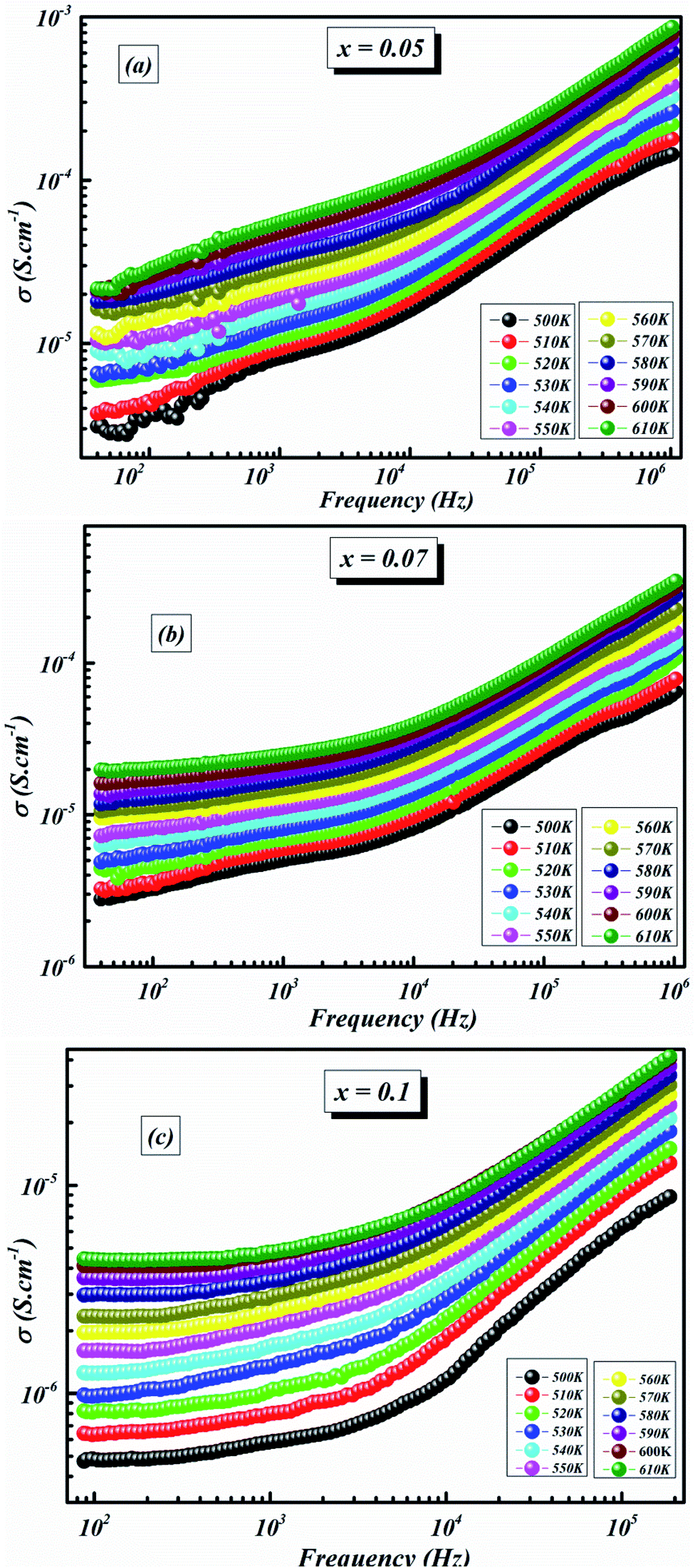
The variation in conductivity as a function of frequency at the designated temperature is shown in Fig. 7(a–c). In these graphs of experimental data, it can be seen from the curves that there are effectively two specific areas. Especially, at low frequencies, the first is related to the continuous conductivity (DC) which has remained roughly constant. In another part, the second is identical to the alternating conductivity (AC), which relies heavily on the frequency of the higher ones. The evolution of the alternating current reveals the presence of a thermally activated process caused by the increase in the energy of the charge carrier.41 As indicated by Jonscher’s universal power law, electrical conductivity can be described by:42
| σToT = σDC + Aωn | (2) |
 | ||
| Fig. 7 Evolution of the electrical conductivity as a function of frequency at different temperatures for BLT0.95Nb0.04 (a), BLT0.93Nb0.056 (b) and BLT0.9Nb0.08 (c). | ||
In eqn (2), σDC and Aωn express the (σAC) conductivity in continuous and alternating currents, respectively. A is a constant for a particular temperature. n defines an exponent subject to temperature and frequency. The study of exponent comportment n(T) is the useful solution. Its variation gives rise to different models.
Also, the decrease of grain size with increasing Nb content (see Fig. 3(a–c) and discussion of SEM) results in increased grain boundaries and hence less transfer of electrons from grain to grain. More substitution of Ti by Nb leads to a decrease of electrical conductivity due to the insulating property of grain boundaries43
The conductivities of different samples are included in the range of semiconductor. We can clearly distinguish the considerable rise in conductivity by the rise in temperature (see Fig. 8). It is reasonably inferred that the higher temperature parts generally generated a higher oxygen vacancy density.44 In this way, the rise in conductivity as the temperature increases can be explained by the increment of space charges, yielded to the inter-grain.45
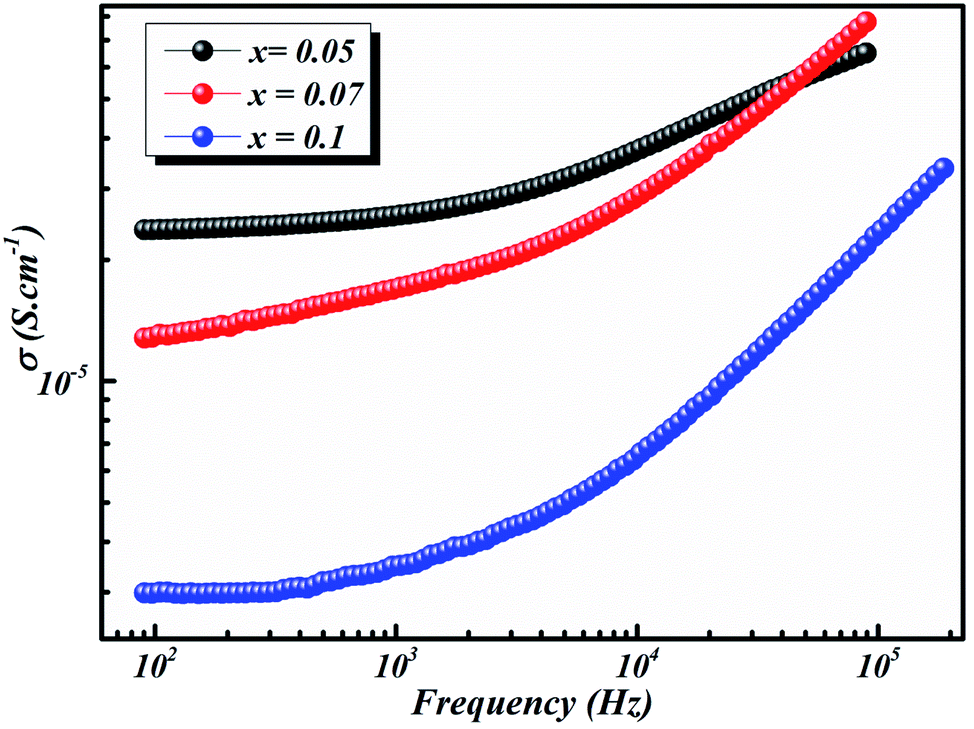 | ||
| Fig. 8 Frequency dependence of conductivity of BLT0.95Nb0.04, BLT0.93Nb0.056 and BLT0.9Nb0.08 samples at 580 K. | ||
A transition occurs which can be attributed to the presence of impurities and the slight growth of grains and grain boundaries.46 The behavior of semiconductors in our polycrystalline compounds is definitely characterized by the increase in conductivity with temperature.
As the temperature decreases the value of AC conductivity also decreases (cf. Fig. 8). The AC conductivity is found to be of the order of 10−3 S cm−1 at 580 K for x = 0.05 and it decreases to the order of 10−5 S cm−1 for x = 0.07. Our results are in good agreement with the results obtained by Singh et al.47 Also, the values of activation energy for various x values indicated that the activation energy for facilitating AC conductance is related to the motion of the dipoles and the dielectric loss behavior at different frequencies.48
The plot in Fig. 8 unveils two distinct regions: the low-frequency region and the high frequency region. At low frequencies, a plateau which characterizes the direct current conductivity is present, while at high frequencies, the conductivity increases gradually with increasing frequency and Nb-doping. The behavior of AC conductivity of Nb-doped BLT with temperature and frequency is similar to the observations reported for any other low-mobility crystalline oxide materials and can be attributed to the hopping of charge carriers.49
 | (3) |
Fig. 9(a–c) illustrates the frequency-dependence of the conductivity from 500 K to 610 K.
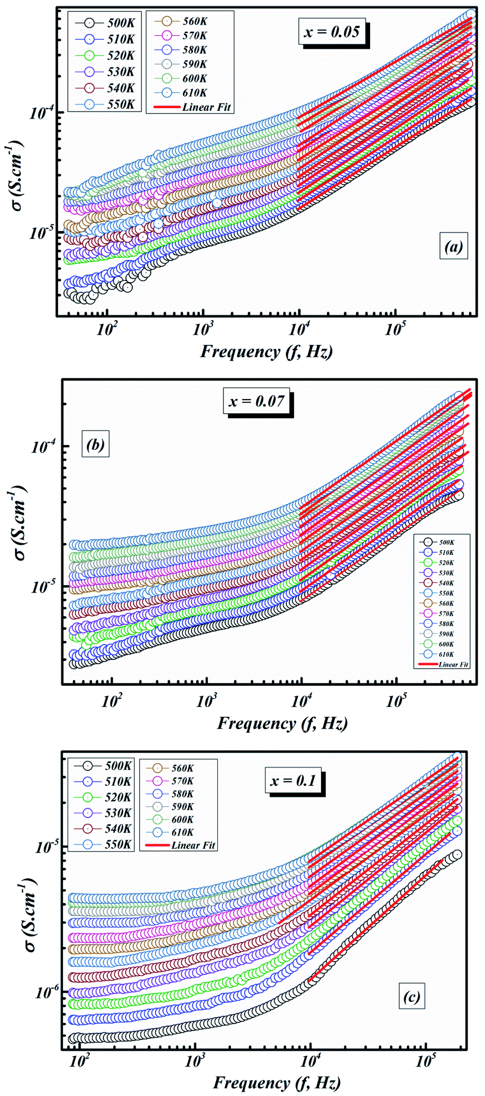 | ||
| Fig. 9 The fit of the electrical conductivity using the universal Jonscher power law for BLT0.95Nb0.04 (a), BLT0.93Nb0.056 (b) and BLT0.9Nb0.08 (c). | ||
Furthermore, a dispersive locale (region II) is noticed at medium frequencies. The AC conductivity advances linearly with the frequency as indicated by the power law Aωn. It interprets the cooperations that influence the movement of load transporters.
As can be seen in Fig. 9(a–c), the value of σAC increases with increasing frequency. This σAC contributes only to the dielectric loss, which becomes infinite at zero frequency and not important at high frequencies. As the frequency increases, σAC increases because the polarization decreases with increasing frequency. Increase in the σAC also leads to an increase of the eddy current which in turn increases the energy dielectric loss. This result is also compatible with the literature, where it is suggested that the increase in σAC with increasing frequency is attributed to the gradual decrease in resistance.51–53 As a result, the change in the AC electric conductivity (σAC) is a result of restructuring and reordering of charges at the sample’s interface under external electric field or temperature and interface polarization.
Different models to explain the conduction methods of AC conductivity with n(T) in various materials have been presented in the literature survey, for example:
– The overlapping-large polaron tunneling (OLPT) model, applied when the exponent “n” decreases with the rise in the temperature until reaching a minimum value, then increases when the temperature increases.54
– The non-overlapping small polaron tunneling (NSPT) model; the exponent n increases as the temperature increases.55
– The correlated barrier hopping (CBH) model; the exponent n decreases as the temperature increases.56
– The tunneling quantum mechanics (QMT) model; the exponent n is almost constant around a value of 0.8 and increases softly with increasing temperature.57
In order to determine the most suitable conduction mechanism of the ac conductivity for the BLT1–xNb4x/5 sample, the study of exponent comportment n(T) is the useful solution. Its variation gives rise to different models:
3.4.1.1 CBH model. In this model, the conduction is affected by the skipping of electrons, trapped in two defect centers, over a Coulomb barrier that disconnects or isolates it. The CBH model was revealed in 1972 by Pike56 for the jumping of a single electron. In 1977, Elliot extended this model for the simultaneous jumping of two electrons.58 The height of the barrier is associated to the distance isolating the two defect states through coulomb interactions. For adjacent sites (decrease of separation R) the potential wells overlap, leading to a lessening of the barrier height from Wm to W given by:
 | (4) |
 | (5) |
 | (6) |
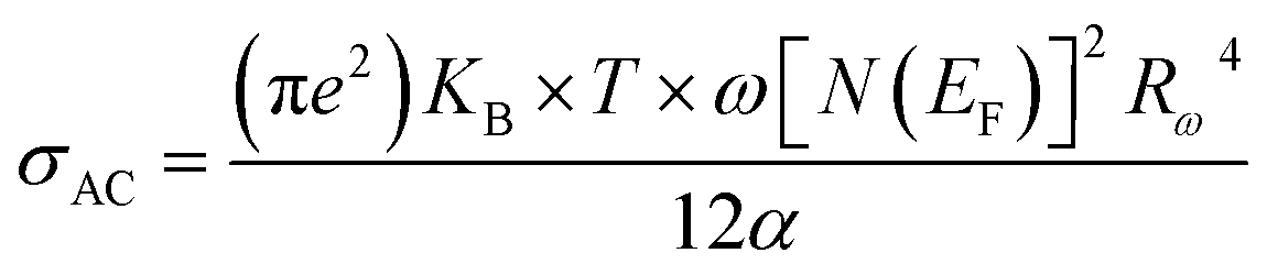
The AC conductivity in the CBH model is articulated as follows:60
 | (7) |
 | (8) |
The DC conductivity of the CBH model was assessed by Pramanik et al.62 where the development of charge carriers is not constrained to pairs of locales; rather it stretches out to the contribution of different states with the intercession of percolation conditions. The DC conductivity is given by:
 | (9) |
3.4.1.2 NSPT model. In a covalent solid, the addition of the charge transporters to a site brings about a local distortion of the lattice. The organization of electrons and its nearby distortion forms a polaron; and the energy of the states is reduced by a quantity Wp (the polaron energy). In the “small polaron” these particles are limited to the point that their distortion clouds do not overlap. In this case, the electron tunnels between the states near the Fermi level, and the tunneling energy is characteristically expressed by WH ≈ (1/2)Wp which is independent of the inter-site separation. In the NSPT model, the exponent “n” is given by:63
 | (10) |
For the approximation of large values of WH/KBT, the expression of “n” is expressly reduced to:
 | (11) |
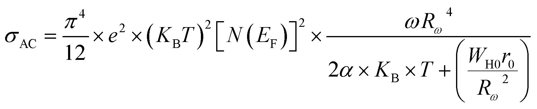
According to NSPT model, the AC conductivity is principally given by the formula:63
 | (12) |
 | (13) |
The tunneling distance diminishes with increasing frequency until arriving at the very minimum value, which can’t be equal to zero, yet is equivalent to the interatomic dispersal.
3.4.1.3 OLPT model. The overlapping-large polaron tunneling occurs when the polaron distortion clouds overlap.
The name “large polaron” comes from the large spatial extent of the polaron wells in comparison to the interatomic distances. The overlap of two neighboring wells brings about the lowering of the polaron transfer energy according to:
 | (14) |
 | (15) |
 | (16) |
 | (17) |
Rω is the tunneling distance at a frequency ω, mathematically, given by the following expression:60
 | (18) |
3.4.1.4 QMT model. For the quantum mechanical tunnel model, conduction generally occurs by tunneling of electrons between defect states near the Fermi level without polaron formation. This model is characterized by the temperature independence of the significant exponent “n” given by:66
 | (19) |
For a typical values of τ0 = 10−13 s and ω = 104 s−1, a value of nQMT ≈ 0.8 is obtained. The AC conductivity, according to QMT model, is expressed by the following formula:67
 | (20) |
 | (21) |
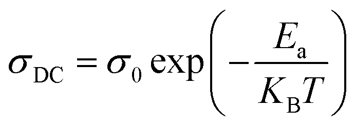
The DC conductivity of the tunneling models obeys the Mott law where σDC varies according to exp(−T−1/4) which is supposed to result from variable-range phonon-assisted tunneling between localized states.60,63
According to eqn (2), it is clear that σtot(ω) is frequency-dependent in the high frequency range; these linear dependencies of AC electrical conductivity with frequency could account for the electron conduction via a hopping process between coordinating sites, local structural relaxations and segmental motions of the compound.68 In order to determine the conduction mechanism, the values of the exponent, n, were deduced for all samples at different temperatures and plotted against temperature.
3.4.1.5 BLT0.95Nb0.04. Fig. 10(a) presents the variation of the exponent “n” which increases with increasing in temperature (in the region 500–570 K) and then decreases (570–610 K); this suggests that two conduction mechanisms are existed. Thus, the change in the ac electric conductivity (σac) is a result of restructuring and reordering of charges for the ceramic compound interface under temperature and interface polarization. Also, the values of activation energy for x = 0.05 indicated that the activation energy proves the existence of two conduction mechanisms in the temperature range from 500–570 K and 570–610 K is related to the motion of the dipoles behavior at different frequencies.48 Thus, according to these variations, NSPT and CBH models are the appropriate models, respectively. The polaron hopping energy Wh for the NSPT model was calculated from the linear fit of the experimental data 1 − n vs. T and it was Wh = 0.311 eV. The barrier height Wm for the CBH model was calculated in the same way and it was Wm = 0.476 eV (see Fig. 10(d)).
3.4.1.6 BLTi0.93Nb0.056. NSPT is the suitable conduction model in this sample, which is proved by the rise of “nNSPT ” as a function of temperature (see Fig. 10(b)). The value of Wh is found to be equal to 0.208 (see Fig. 10(e)).
It is well noticed that the height of the barrier for each model decreases by increasing the sintering temperature. Thus, the transport of the electrons or polarons is facilitated resulting consequently in the increase of the conductivity.
3.4.1.7 BLT0.9Nb0.08. The evolution of the frequency exponent “nCBH” versus temperature appears in the Fig. 10(c). This result implies that the CBH model (the barrier height Wm is found to be 0.106 eV) and the NSPT model (the polaron hopping energy Wh was calculated to be equal to 0.140 eV) are the closely excellent theoretical models to describe the electrical conduction mechanism in our BLT0.9Nb0.08 ceramic (from the linear fit of the experimental data 1 − n vs. T (see Fig. 10(f))).
The frequency-dependent AC conductivity at different temperatures indicates that the conduction process is thermally activated. The AC conductivity is found to obey the universal power law and the CBH and NSPT models are found to successfully explain the mechanism of charge transport in the Nb-doped BLT1−xNb4x/5O3. Low values of polaron binding energy W calculated using the experimental values of the frequency exponent n confirm the existence of the transport of the electrons or polarons. The decrease in the density of states with increasing Nb content indicates an increase in the delocalization, which is deemed responsible for the increase in the AC conductivity.
The values of AC activation energy Ea are obtained at different frequencies as previously calculated from the Arrhenius equation and listed in Fig. 11a. It is noted that the values of σtot(ω) are higher than σDC and EAC are lower than EDC. This can be due to the fact that the increase in the applied field frequency enhanced the electron mobility and, subsequently, the conductivity value.58,69 In addition, the loss factor dominates at higher frequencies and, therefore the conductivity increases up to comparatively higher values for higher frequency ranges.70,71 The decrease in the total conductivity at higher temperatures may be due to the scattering of electrons which is the dominant behavior by increasing temperature.72
The temperature dependence of AC conductivity at various frequencies, for example x = 0.05, is revealed in Fig. 11b. The conductivity is increased with rising temperature. The temperature-dependent conductivity of the ceramic exhibits an Arrhenius behavior.73 The AC conductivity dependence of temperature of the ceramic can be written as
 | (22) |
This leads us to propose that the applied field frequency enhances the electronic jumps stuck between the localized states and that is why activation energy diminishes with frequency. The smaller activation energy values and increases in the AC conductivity with rising frequency confirm the hopping to be the dominant conduction mechanism.
 | (23) |
For our synthetic ceramic compounds, by plotting log(σDC) against 1/T or 1/T−1/4, we obtain a straight line with a slope over all the temperature sequences. The adjustment of the experimental results could be carried out by Arrhenius or Mott’s law. The adjustment R square values are established in Fig. 10(d–f) for Ba0.97La0.02Ti1−xNb4x/5O3 (x = 5, 7 and 10, in mol%), respectively.
 | ||
| Fig. 10 (a–c) Variations of exponent n and (d–f) n − 1 with temperature for BLT0.95Nb0.04, BLT0.93Nb0.056 and BLT0.9Nb0.08. | ||
 | ||
| Fig. 11 (a) Variation of (σT) as a function of temperature for x = 0.05 (b) plots of lnσACT vs. 1/T1/4 of x = 0.05 at different frequencies. | ||
 | ||
| Fig. 12 (a–c) Variation of (σT) as a function of temperature of Ba0.97La0.02Ti1−xNb4x/5O3, respectively, for x = 0.05, x = 0.07 and x = 0.1. (d–f) The evolution of log(σT) against 1/T1/4 of BLT0.95Nb0.04, BLT0.93Nb0.056 and BLT0.9Nb0.08. | ||
4. Conclusion
Frequency- and temperature-dependent conductivity measurements for our polycrystalline perovskite ceramic systems with a composition of Ba0.97La0.02Ti1−xNb4x/5O3 (x = 5, 7 and 10, in mol%) were performed. Our perovskite polycrystalline compounds have been prepared by a high-temperature molten-salt reaction technique. Preliminary X-ray diffraction results prove the tetragonal crystal structure at room temperature. The morphology of the samples was studied through TEM, which gives the average grain size on the order of 5 μm. The electrical behavior of the polycrystalline compounds was investigated by impedance spectroscopy in the 500–610 K temperature range. The conductivity analysis reveals a distinguished increase with increasing Nb content. Besides, the electrical conductivity obeys Jonscher’s universal power law. For the AC conductivity, the evolution of the exponent s with temperature indicates the presence of NSPT and CBH models as dominant conduction processes in our materials. An increase in DC conductivity (i.e., bulk and grain boundary) with rising temperature is also observed.Conflicts of interest
The authors (M. Jebli, Ch. Rayssi, J. Dhahri, M. Ben Henda, Hafedh. Belmabrouk and Abduallah Bajahzar) declare that there are no conflicts of interest regarding this manuscript.References
- F. Jona and G. Shirane, Ferroelectric crystals, Dover Publications, INC., New York, 1993 Search PubMed.
- G. H. Jonker, Solid-State Electron., 1964, 7, 895 CrossRef CAS.
- H. M. Chan, M. P. Harmer and D. M. Smyth, J. Am. Ceram. Soc., 1986, 69, 507 CrossRef CAS.
- C. J. Ting, C. J. Peng, H. Y. Lu and S. T. Wu, J. Am. Ceram. Soc., 1990, 73, 329 CrossRef CAS.
- R. Wernicke, Phys. Status Solidi B, 1978, 47, 139 CrossRef CAS.
- A. M. Muller and K. H. Hardtl, Appl. Phys. A, 1989, 49, 75 CrossRef.
- N. G. Eror and D. M. Smyth, in The Chemistry of Extended Defects in Non-metallic Solids, ed. L. R. Eyring and M. O’Keeffee, North-Holland, Amsterdam, 1970, p. 62 Search PubMed.
- N. H. Chan and D. M. Smyth, J. Am. Ceram. Soc., 1984, 67, 285 CrossRef CAS.
- N. H. Chan, R. K. Sharma and D. M. Smyth, J. Am. Ceram. Soc., 1981, 64, 556 CrossRef CAS.
- J. Nowotny and M. Rekas, Ceram. Int., 1994, 20, 265 CrossRef CAS.
- K. Kowalski, M. Ijjaali, T. Bak, B. Dupre, J. Nowotny, M. Rekas, C. C. Sorrell and Y. Zhao, J. Phys. Chem. Solids, 2001, 62, 531–535 CrossRef CAS.
- G. H. Jonker and E. E. Havinga, Mater. Res. Bull., 1982, 17, 345 CrossRef CAS.
- J. Daniels and K. H. Hardtl, Philips Res. Rep., 1976, 31, 489–504 CAS.
- K. Kowalski, M. Ijjaali, T. Bak, B. Dupre, J. Nowotny, M. Rekas, C. C. Sorrell and Y. Zhao, J. Phys. Chem. Solids, 2001, 62, 537–541 CrossRef CAS.
- Y. W. Hu, P. P. Yong, L. C. Xiao and F. W. Jin, Study of reoxidation in heavily La-doped barium titanate ceramics, J. Phys.: Conf. Ser., 2009, 152, 012040 CrossRef.
- K. Alioune, L. A. Guehria, A. Simon and J. Ravez, Study of new relaxor materials in BaTiO3-BaZrO3-La2/3TiO3 system, Solid State Sci., 2005, 7, 1324–1332 CrossRef.
- M. Ganguly, S. K. Rout and T. P. Sinha, Characterization and Rietveld refinement of A-site deficient lanthanum doped barium titanate, J. Alloys Compd., 2013, 579, 473–484 CrossRef CAS.
- P. Dhak, D. Dhak, M. Das, K. Pramanik and P. Pramanik, Mater. Sci. Eng., B, 2009, 164, 165–171 CrossRef CAS.
- Y. Wang, K. Miao, W. Wang and Yi Qin, J. Eur. Ceram. Soc., 2017, 37, 2385–2390 CrossRef.
- T. Dechakupt, J. Tangsritrakul, P. Ketsuwan and R. Yimnirun, Ferroelectrics, 2011, 415, 141–148 CrossRef CAS.
- S.-H. Yoon and J. Hwan Kim, Appl. Phys., 2002, 92, 1039 CAS.
- R. Mahbub, Md. Sazzad Hossain and Md. Fakhrul Islam, Materiálové inžinierstvo (MEMI) Journal, 2013, 20, 45–53 Search PubMed.
- R. N. Basu and H. S. Maiti, Mater. Res. Bull., 1986, 21(9), 1107 CrossRef.
- M. Jebli, et al., Frequency and thermal studies of dielectric permittivity and Raman analysis of Ba0.97La0.02Ti0.98Nb0.016O3, J. Mater. Sci.: Mater. Electron., 2020, 31(24), 22323–22339 CrossRef CAS.
- H. Saadi, et al., Enhancing the electrical and dielectric properties of ZnO nanoparticles through Fe doping for electric storage applications, J. Mater. Sci.: Mater. Electron., 2021, 1–21 Search PubMed.
- M. Jebli, et al., Raman spectra, photoluminescence, and low-frequency dielectric properties of Ba0.97La0.02Ti1−xNb4x/5O3 (x = 0.00, 0.05) ceramics at room temperature, J. Mater. Sci.: Mater. Electron., 2020, 31(18), 15296–15307 CrossRef CAS.
- D. Y. Lu, M. Sugano and M. Toda, High-permittivity double rare earth-doped barium titanate ceramics with diffuse phase transition, J. Am. Ceram. Soc., 2006, 89, 3112–3123 CrossRef CAS.
- N. Horchidan, et al., J. Alloys Compd., 2011, 509, 4731–4737 CrossRef CAS.
- M. Jebli, et al., Effect of Nb-doping on the structural and electrical properties of Ba0.97La0.02Ti1−xNb4x/5O3 ceramics at room temperature synthesized by molten-salt method, J. Alloys Compd., 2019, 784, 204–212 CrossRef CAS.
- V. Chauhan, et al., J. Alloys Compd., 2016, 674, 413–424 CrossRef CAS.
- P. G. Radaelli, G. Iannone, M. Marezio, H. Y. Hwang, S.-W. Cheong, J. D. Jorgensen and D. N. Argyriou, Phys. Rev. B: Condens. Matter Mater. Phys., 1997, 56, 8265 CrossRef CAS.
- J. Nowotny, in, CRC Handbook on Solid State Electrochemistry, ed. P. J. Gellings and H. J. M. Bouwmeester, CRC Press, Boca Raton, 1997, p. 121 Search PubMed.
- J. Nowotny and C. C. Sorrell, Electrical Properties of Oxide Materials, Trans Tech Publications, Zurich, 1997 Search PubMed.
- W. R. Buessem and M. Kahn, J. Am. Ceram. Soc., 1971, 54, 458 CrossRef CAS.
- O. Saburi, J. Phys. Soc. Jpn., 1959, 14, 1159 CrossRef CAS.
- D. Hennings, Int. J. High Technol. Ceram., 1987, 3, 91 CrossRef CAS.
- G. H. Jonker and E. E. Havinga, Mater. Res. Bull., 1982, 17, 345 CrossRef CAS.
- A. M. J. H. Seuter, Philips Res. Rep., Suppl., 1974, 3, 1 Search PubMed.
- J. Nowotny and M. Rekas, Ceram. Int., 1994, 20, 225 CrossRef CAS.
- S. Karoui and S. Kamoun, Int. J. Sci. Res., 2015, 4, 2201–2210 Search PubMed.
- S. Hajlaoui, I. Chaabane and K. Guidara, RSC Adv., 2016, 6, 91649–91657 RSC.
- A. K. Jonscher, J. Phys. D: Appl. Phys., 1999, 57, 32 Search PubMed.
- Ch. Rayssi, F. I. H. Rhouma, J. Dhahri, K. Khirouni, M. Zaidi and H. Belmabrouk, Appl. Phys. A, 2017, 123, 778 CrossRef CAS.
- C.-M. Wang, K.-S. Kao, S.-Y. Lin, Y.-C. Chen and S.-C. Weng, J. Phys. Chem. Solids, 2008, 69, 608–610 CrossRef CAS.
- L. Fang and M. Shen, J. Appl. Phys., 2004, 95, 6483–6485 CrossRef CAS.
- W. Yang, S. Yu, R. Sun and R. Du, Acta Mater., 2011, 59, 5593–5602 CrossRef CAS.
- P. K. Singh and A. Chandra, The effect of ferroelectric ceramics materials Ba0.70Sr0.30TiO3 and Ba0.88Sr0.12TiO3, J. Phys. D: Appl. Phys., 2003, 36, 193–196 CrossRef.
- W.-S. Kang, et al., Ceram. Int., 2015, 41, 6925–6932 CrossRef CAS.
- V. Gupta and A. Mansingh, Phys. Rev. B: Condens. Matter Mater. Phys., 1994, 49, 1989 CrossRef CAS PubMed; A. Mansingh, Bull. Mater. Sci., 1980, 16, 2325 Search PubMed.
- J. Hao, et al., J. Am. Ceram. Soc., 2012, 95(6), 1998–2006 CrossRef CAS.
- I. M. Afandiyeva, M. M. Bülbül, S. Altındal and S. Bengi, Microelectron. Eng., 2012, 93, 50 CrossRef CAS.
- A. A. Sattar and S. A. Rahman, Phys. Status Solidi, 2003, 200, 415 CrossRef CAS.
- P. Dutta, S. Biswas and S. K. De, Mater. Res. Bull., 2002, 37, 193 CrossRef CAS.
- A. Ghosh and D. Chakravorty, J. Phys.: Condens. Matter, 1990, 2, 5365–5372 CrossRef CAS.
- X. Cleac’hJ, Phys, 1979, 40, 417–428 Search PubMed.
- G. E. Pike, Phys. Rev. B: Solid State, 1972, 6, 1572–1580 CrossRef CAS.
- S. R. Elliott, Philos. Mag. B, 1978, 36, 129 Search PubMed.
- S. R. Elliott, Philos. Mag., 1977, 36, 1291–1304 CrossRef CAS.
- M. Ben Bechir, K. Karoui, M. Tabellout, K. Guidara and A. Ben Rhaiem, J. Appl. Phys., 2014, 115, 203712 CrossRef.
- S. R. Elliott, Adv. Phys., 1987, 36, 135–218 CrossRef CAS.
- Y. Ben Taher, A. Oueslati, K. Khirouni and M. Gargouri, Mater. Res. Bull., 2016, 78, 148–157 CrossRef CAS.
- M. H. A. Pramanik, P. N. Butcher and I. D. Cox, Philos. Mag. B, 1983, 47, 437–443 CAS.
- A. R. Long, Adv. Phys., 1982, 31, 553–637 CrossRef CAS.
- A. Zaafouri and M. Megdiche, Ionics, 2017, 23, 1155–1164 CrossRef CAS.
- A. Ghosh, Phys. Rev. B: Condens. Matter Mater. Phys., 1990, 41, 1479–1488 CrossRef CAS PubMed.
- S. R. Elliott, Philos. Mag. B, 1978, 37, 553–560 CAS.
- S. Mollah, K. K. Som, K. Bose and B. K. Chaudhuri, J. Appl. Phys., 1993, 74, 931–937 CrossRef CAS.
- A. Ghosh, Ac conduction in iron bismuthate glassy semiconductors, Phys. Rev. B: Condens. Matter Mater. Phys., 1990, 42, 1388 CrossRef CAS PubMed.
- M. El-Shaarawy, A. Mansour, S. El-Bashir, M. El-Mansy and M. Hammam, Electrical conduction and dielectric properties of poly(methyl methacrylate)/perylene solar concentrators, J. Appl. Polym. Sci., 2003, 88, 793–805 CrossRef CAS.
- A. K. Jonscher, Dielectric relaxation in solids, J. Phys. D: Appl. Phys., 1999, 32, R57 CrossRef CAS.
- A. K. Jonscher, The universal dielectric response, Nature, 1977, 267(5613), 673–679 CrossRef CAS.
- D. A. Seanor, Electrical Properties of Polymers, Elsevier, 2013 Search PubMed.
- S. Kumar and K. B. R. Varma, Solid State Commun., 2008, 146, 137 CrossRef CAS.
| This journal is © The Royal Society of Chemistry 2021 |