
 Open Access Article
 This Open Access Article is licensed under a Creative Commons Attribution-Non Commercial 3.0 Unported Licence
High rate fabrication of copper and copper–gold electrodes by laser-induced selective electroless plating for enzyme-free glucose sensing
Evgeniia M. Khairullinaa,
Maxim S. Panov a,
Vladimir S. Andriianova,
Karolis Ratautasb,
Ilya I. Tumkin*a and
Gediminas Račiukaitisb
a,
Vladimir S. Andriianova,
Karolis Ratautasb,
Ilya I. Tumkin*a and
Gediminas Račiukaitisb
aSaint Petersburg State University, 7/9 Universitetskaya nab., St. Petersburg 199034, Russia. E-mail: i.i.tumkin@spbu.ru
bCenter for Physical Sciences and Technology, 231 Savanoriu ave., Vilnius 02300, Lithuania
First published on 30th May 2021
Abstract
In the current study, the method of Selective Surface Activation Induced by Laser (SSAIL) was used for the fabrication of metallic and bimetallic structures based on copper and gold on the surface of glass and glass-ceramics. It was shown that the fabricated electrodes are suitable for non-enzymatic detection of biologically essential analytes such as glucose. The implemented approach allows performing high-rate metallization of various dielectrics. Voltammetric methods were applied to evaluate the electrocatalytic activity of the obtained structures, which were used as working electrodes. The most promising results were revealed by copper–gold electrode structures manufactured on glass-ceramics. For these structures, sensitivity towards glucose sensing was 3060 μA mM−1 cm−2. The linear range of glucose detection varied between 0.3 and 1000 μM. Besides, the manufactured electrodes exhibited high selectivity and long-term stability.
Introduction
It is difficult to overestimate the importance of monitoring various bioanalytes in human blood. Recent advances in science and technology provide the necessary conditions for the efficient treatment and diagnosis of many diseases, including diabetes, hypertension, atherosclerosis, cancer and Parkinson's disease.1–3 Sensors for the detection of glucose deserve special attention in this regard.4,5 Measuring the concentration of glucose in human blood is quite important, and many diabetic patients around the world have an opportunity to significantly improve their quality of life using modern glucose meters.6 The devices for invasive blood glucose monitoring are widely available on the market and are in great demand. Typically, such sensors are based on electrochemical or optical glucose detection. In the electrochemical approach, this process is typically realised by enzymatic oxidation of glucose. Such an approach has several significant disadvantages such as low detection accuracy, poor stability as a result of enzyme decomposition, relatively low selectivity and short service time due to high sensitivity to pH and humidity.7Modern sensors and biosensors8 should satisfy plenty of requirements such as durability, ability to operate in physiological conditions, mechanical stability, high selectivity and others. Therefore, the development of new methods for the fabrication of materials suitable for sensing many types of bioanalytes is a very relevant scientific and technological challenge. Furthermore, there is a reasonably good alternative to enzyme-based sensors that deals with direct detection of the biologically essential substances. In the case of such non-enzymatic detection, the use of enzymes is not required, and oxidation of an analyte (e.g., glucose) is achieved via catalytic ox-red reactions taking place on the surface of the highly developed electrode structure.9–16 In addition, it is possible to increase the surface area of these electrodes by modifying them with catalytically active nanostructures based on biocompatible metals such as gold, platinum, iridium etc., which considerably improves their electrochemical characteristics (sensitivity, selectivity and stability).17–23
There is a significant number of modern methods that can be applied for the purposes mentioned above: inkjet printing,24 screen printing,25 roll-to-roll printing (R2R),26 chemical vapour deposition (CVD),27 photoelectrochemical methods28,29 etc. Among them, the techniques based on laser technologies are of the greatest interest. For example, the method of laser-induced chemical liquid phase deposition (LCLD)30–32 allows to deposit micro-sized metal structures on the surface of various dielectrics by reduction of metal ions in a local volume of a solution within the focus of the laser beam. Similar to LCLD, direct laser writing (DLW)33 also enables synthesising metallic structures. It is known that Laser Induced Forward Transfer (LIFT) can be used for manufacturing nano/micro patterns suitable for sensor applications.34 Thus, due to unique characteristics, including high spatial resolution and fast implementation, LIFT was successfully applied for fabrication of chemical sensors based on copper, gold and other metals. Another striking example of laser-induced methods is selective laser sintering (SLS).35,36 SLS is an additive technology for synthesis of three-dimensional structures of a given size and shape occurring due to laser-assisted heating powders of different materials up to temperature, at which particles of these powders stick together. There are several methods for ink paste sintering, but all of them have many similar procedures. Non-conductive ink solution based on metal compounds is reduced to metal atoms by laser irradiation. Kang et al.37 made ink paste by dispersing copper oxide (CuO) particles into a reducing agent solution. Ytterbium-doped fibre laser was used for irradiation of the deposited layer. Both pulsed nanosecond and CW lasers have been applied. Photon energy of the irradiating laser has photon energy high enough to brake Cu–O bonds. After bond breaking, a reduction of Cu ions by ethylene glycol takes place. The results of such studies have been confirmed by Energy Disperse Spectroscopy (EDS). It should be mentioned here that around 90% of Cu ions could be reduced by pulse laser irradiation. In another work carried out by Chen et al.,38 PI films were treated by KOH solution. As a result, PI became hydrolysed and potassium polyamine was generated. Later, the specimen was immersed in the AgNO3 solution. Therefore, Ag ions exchanged potassium ions. Laser writing was performed by Nd:YAG laser nanosecond laser with the IV harmonics wavelength. After laser irradiation, the Ag ions were reduced to Ag0.38 The disadvantages of both processes are very similar and related to the difficulties of thin layer deposition. Another method for selective metal deposition on the surface is Laser Direct Structuring (LDS). LDS is the method using precursors mixed in a polymer matrix.39 These precursor additives are activated during the laser writing process by converting them into a catalyst for electroless deposition of the metal. Thus, the laser-treated area could be selectively plated.39 There are a few commercial materials for LDS available on the market. However, most of the LDS polymers are based on expensive metal–organic fillers, such as palladium-based metal–organic compounds or microparticles of copper oxide spinel crystal.39 Moreover, it is possible to combine LIFT technology (laser printing) and laser sintering to produce copper patterns with better electrical properties because of minimizing oxidation effects.40 For that purpose, an ink based on copper nanoparticles pre-synthesized from copper chloride, polyvinylpyrrolidone and sodium borohydride as a reducing agent were used.
The methods mentioned above are appropriate for metallization of many types of substrates. Some of them are used for fabrication of structures with a given pattern (SLS, inkjet printing, screen printing), others only for creating solid coatings and films (CVD). Nevertheless, each of these techniques has several limitations and disadvantages mostly associated with high cost, problems with maintenance, complexity, low efficiency etc.
Considering this, we proposed a versatile method of Selective Surface Activation Induced by a Laser (SSAIL) for metallization of dielectric substrates, which does not require expensive precursors and permits a high fabrication speed.41–43 The process includes laser modification of the polymer surface with a short-pulse laser, chemical activation of the laser-modified areas and electroless metal deposition on the locally activated surface. In the last step (electroless plating), in situ growth of metal particles occurs on the electrode eliminating the necessity for an additional stage of immobilisation or deposition of particles on the surface. The laser processing and electroless plating parameters can control the plating morphology and the size of copper nanostructure. It is also not necessary to add components (e.g., surfactants) to the metallization solution at all stages of the SSAIL that have a significant impact on the fabricated structures. It is worth noting that SSAIL significantly exceeds the laser methods mentioned above (such as LCLD, SLS, etc.) in terms of fabrication speed, because the rate of laser modification of the irradiated surface can reach several meters per second, and the copper plating stage can be performed with a large number of samples simultaneously. Moreover, this process is fully automated; therefore, one can create different patterns and switch between them instantly, if necessary. Another advantage of this method is a strong adhesion of the produced structures to the substrate surface, including polymers, as well as the ability to metallize 3D arbitrary surfaces to create MID devises.
In this work, our goal was to fabricate metallic and bimetallic materials based on copper and gold reliable for non-enzymatic glucose sensing using the SSAIL approach.
Materials and methods
Electrode formation using SSAIL
The Nd:YVO4 picosecond laser Atlantic (Ekspla) with the pulse duration of 10 ps, the pulse repetition rate of 400 kHz to 1 MHz and maximum average power up to 60 W was used for surface modification of the dielectric surface. Pulse picker was used to adjust a lower frequency regime. Translation of the laser beam was performed with a galvanometric scanner (Scanlab AG). The experimental setup is shown in Fig. 1. The F-theta lens of 160 mm focal length was used to focus the laser beam on the surface of a substrate. The laser beam was scanned over the area to be metallized by hatching–overlapping parallel lines. Focused laser beam spot size was 25 μm in diameter (Gaussian intensity level 1/e2).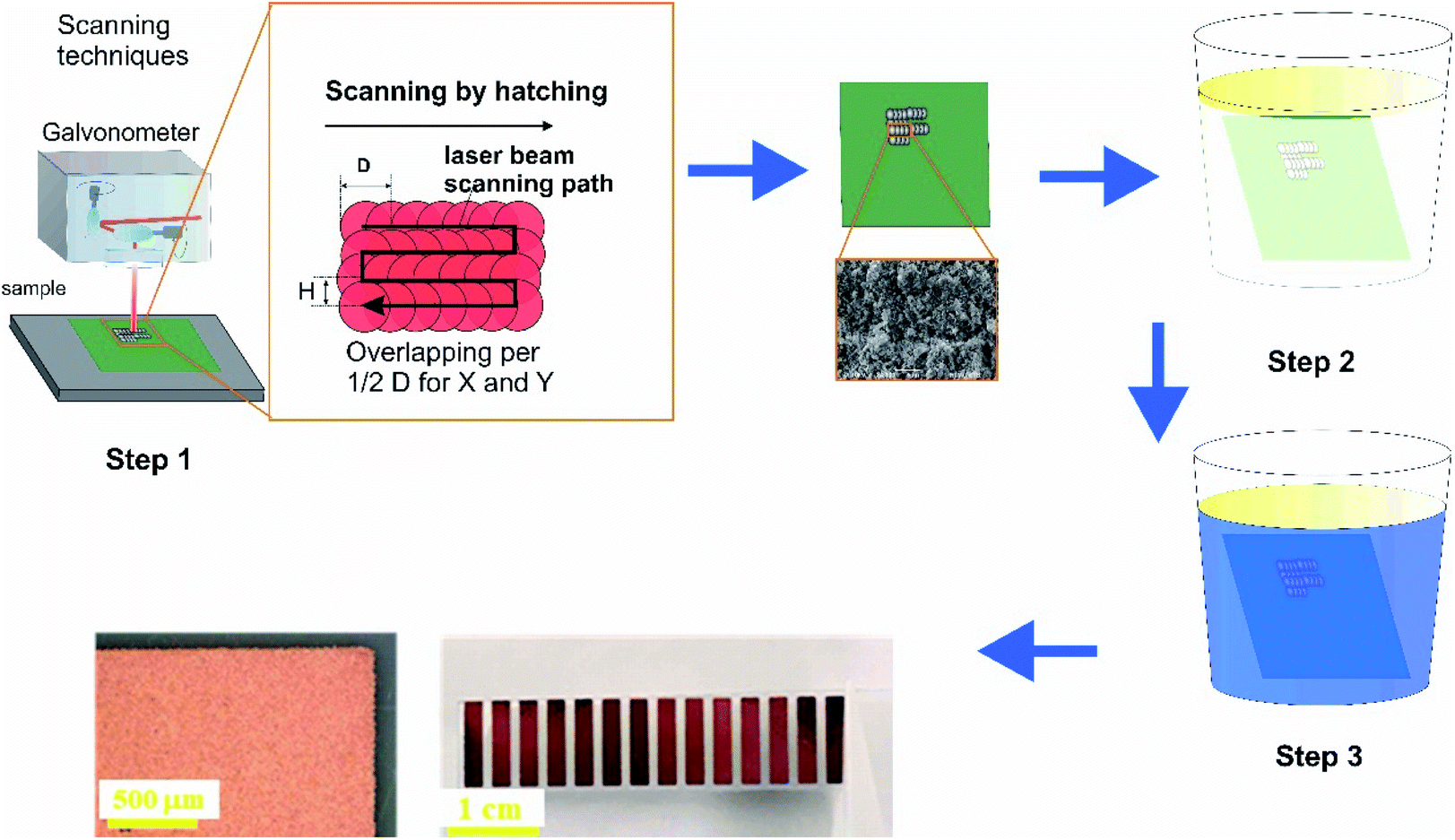 | ||
| Fig. 1 The experimental scheme of laser modification of the dielectric surfaces and their metallization by copper. Step 1: laser modification of the surface to be metallized with Nd:YVO4 pulse picosecond laser, wavelength 532 nm. Step 2: activation with silver nitrate solution (∼10–5 M) for 8 min. Step 3: electroless copper plating: copper(II) sulphate pentahydrate (0.12 M), formaldehyde (0.3 M), sodium hydroxide (1.2 M), sodium carbonate (0.3 M) and sodium–potassium tartrate (0.35), 30 °C for 30 min. | ||
After the laser treatment, all samples were washed with ethanol 99.8% (Sigma-Aldrich) and rinsed with distilled water afterwards. For chemical activation, a highly diluted silver nitrate (Sigma-Aldrich) solution (∼10−5 M) was used. Finally, the electroless copper deposition was performed for 30 min at 30 °C. The copper plating bath contained copper(II) sulphate pentahydrate (0.12 M), formaldehyde (0.3 M), sodium hydroxide (1.2 M), sodium carbonate (0.3 M) and sodium–potassium tartrate (0.35 M) (all Sigma-Aldrich) and pH = 12.7. Finally, copper structures were covered by gold using gold(III) chloride solution in dilute HCl (0.007 M) and 4-(dimethylamino)pyridine (0.1 M) (all Sigma-Aldrich). Gold deposition was carried out by immersing copper-plated substrates in the HAuCl4 (metal source) and DMAP (ligand) water-based solution for 5 minutes at 80 °C. The experiments with variation of temperature and reaction time were performed to reveal the effect of these parameters on topology of the deposits.
Materials
A soda-lime microscopic glass (Sigma-Aldrich) and glass-ceramics were used as a substrate material.Characterisation
The phase composition of the microstructures fabricated using SSAIL was investigated by an X-ray micro-diffractometer (Rigaku RINT RAPID-S) using Cu Kα radiation. The diameter of the X-ray collimator was 0.3 mm. When the X-ray incident angle was 20°, the maximum X-ray irradiation area was approximately 1 × 0.3 mm2.The morphology of the fabricated materials was analysed using scanning electron microscopy (SEM). Their atomic composition was identified by energy dispersion of X-ray spectroscopy (EDX). The EDX-system was coupled with a Zeiss Supra 40VP scanning electron microscope equipped with X-ray attachment (Oxford Instruments INCA X-act).
The electrochemical properties of the produced Cu and Cu–Au structures towards glucose were examined using voltammetric methods (potentiostat, Elins P30I). All measurements were performed at room temperature in a standard three-electrode cell using a platinum wire as a counter electrode, an Ag/AgCl reference electrode and Cu and Cu–Au microelectrodes as working electrodes. The solutions of D-glucose of different concentrations were added to a background solution (0.1 M sodium hydroxide) with simultaneous stirring.
Results and discussion
To successfully perform surface modification of the dielectric substrates according to the specified electrode geometry and size (in our case, rectangles of 2 × 10 mm), we found the optimal experimental conditions by varying several parameters: average laser power, pulse repetition rate, scanning speed and distance between the adjacent scanned lines–hatch (Table 1). The average laser power was adopted when changing the pulse repetition rate to keep the same pulse energy. The pulse energy varied from 10 to 160 μJ. The hatch distance did not exceed the diameter of the focused laser beam to perform overlapping of the parallel scanned lines. This process of hatching is illustrated in Fig. 1. Scanning electronic images (SEM) of glass and glass-ceramics modified at various experimental conditions are shown in Fig. 2 and 3, respectively. After laser modification, the surfaces of these dielectrics were activated by immersing them for 8 minutes in a silver nitrate solution (5 × 10⁻⁴ M). The final stage involves the chemical deposition of copper on the activated dielectrics, which are placed in an aqueous solution of copper(II) sulfate (0.12 M), formaldehyde (0.3 M), sodium hydroxide (1.2 M) and sodium–potassium tartrate (0.35 M) for 30 minutes at 30 °C. Fig. 2 and 3 show optical images of the glass and glass-ceramics samples taken after metallization by copper at different experimental conditions. The optimal regimes for laser modification of each substrate and their subsequent metallization were selected, based on results of the finally plated surface (Table 2). In addition, all synthesised materials successfully passed the adhesive tape test (scotch test), in which adhesive tape was applied to estimate the adhesion strength of the coating (in this case, copper). After removing the tape, no coating was detached from the substrate surface confirming good adhesion properties of the synthesised materials.| Substrate | Scanning speed (v), m s−1 | Hatch distance (h), μm |
|---|---|---|
| Glass | 0.2, 0.4, 0.6, 0.8 | 10, 15 |
| Glass-ceramics | 0.1, 0.2 | 10, 15 |
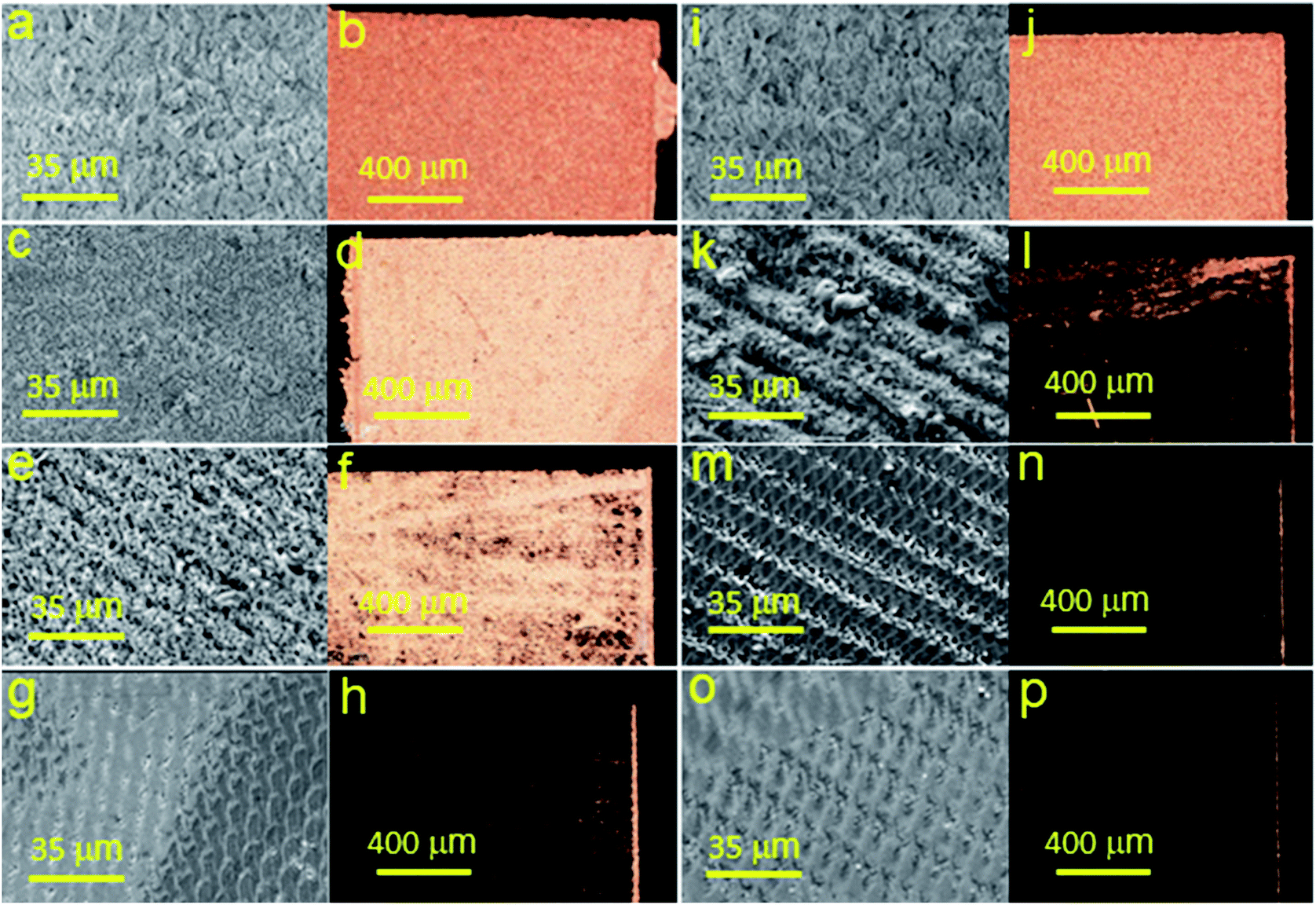 | ||
| Fig. 2 SEM images of glass after laser modification conducted at the following v (m s−1) and h (μm): (a) 0.2 and 10; (c) 0.4 and 10; (e) 0.6 and 10; (g) 0.8 and 10; (i) 0.2 and 15; (k) 0.4 and 15; (m) 0.6 and 15; (o) 0.8 and 15. Optical images of the modified glass after metallization by copper carried out at the following v (m s−1) and h (μm): (b) 0.2 and 10; (d) 0.4 and 10; (f) 0.6 and 10; (h) 0.8 and 10; (j) 0.2 and 15; (l) 0.4 and 15; (n) 0.6 and 15; (p) 0.8 and 15. | ||
 | ||
| Fig. 3 SEM images of glass-ceramics after laser modification conducted at the following v (m s−1) and h (μm): (a) 0.1 and 10; (c) 0.2 and 10; (e) 0.1 and 15; (g) 0.2 and 15. Optical images of the modified glass-ceramics after metallization by copper carried out at the following v (m s−1) and h (μm): (b) 0.1 and 10; (d) 0.2 and 10; (f) 0.1 and 15; (h) 0.2 and 15. | ||
| Substrate | Laser power, W | Repetition rate, kHz | Scanning speed, m s−1 | Hatching size, μm |
|---|---|---|---|---|
| Glass | 6.23 | 100 | 0.2 | 15 |
| Glass-ceramics | 0.61 | 10 | 0.1 | 15 |
Furthermore, morphology and elemental analysis of the fabricated copper structures on glass and glass-ceramics were investigated using SEM and EDX, respectively (Fig. 4 and 5). For each material, EDX spectra were recorded at different locations to determine the atomic composition more accurately. SEM images were taken with a magnification of 100![[thin space (1/6-em)]](https://www.rsc.org/images/entities/char_2009.gif) 000, 25000 and 1000 for all samples. The surface morphology of the samples of both substrates was different, showing chaotic crystal formation ranging in a size from several hundred nm to several microns. All studied materials consisted of copper (97–100%), in turn, the presence of oxygen, magnesium and calcium demonstrated in Fig. 4 can be explained by the material of the substrate (glass). It is also suggested that the substrate material may affect the probability of formation of a monolithic deposit on its surface. X-ray diffraction analysis (XRD) was performed to clarify this assumption and reveal the phase composition of each sample. The results of these studies are presented in Fig. 6a and b. It was shown that individual copper peaks are present in each X-ray diffractogram. The presence of copper(I) and copper(II) oxides peaks can be referred to incomplete copper reduction reaction in a solution and/or oxidation of the material surface by air oxygen during storage.
000, 25000 and 1000 for all samples. The surface morphology of the samples of both substrates was different, showing chaotic crystal formation ranging in a size from several hundred nm to several microns. All studied materials consisted of copper (97–100%), in turn, the presence of oxygen, magnesium and calcium demonstrated in Fig. 4 can be explained by the material of the substrate (glass). It is also suggested that the substrate material may affect the probability of formation of a monolithic deposit on its surface. X-ray diffraction analysis (XRD) was performed to clarify this assumption and reveal the phase composition of each sample. The results of these studies are presented in Fig. 6a and b. It was shown that individual copper peaks are present in each X-ray diffractogram. The presence of copper(I) and copper(II) oxides peaks can be referred to incomplete copper reduction reaction in a solution and/or oxidation of the material surface by air oxygen during storage.
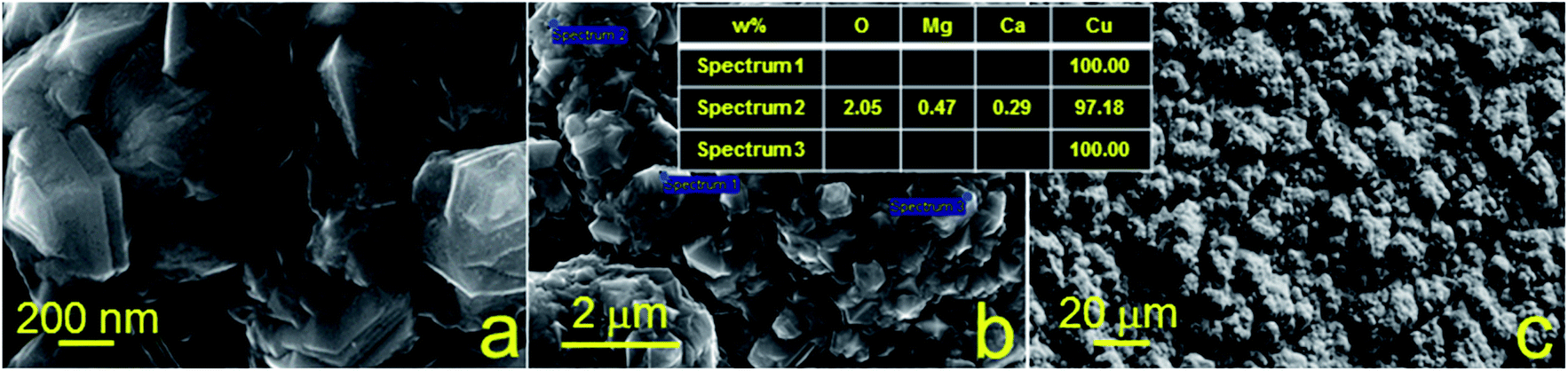 | ||
| Fig. 4 SEM images and EDX analysis of copper structures fabricated using SSAIL on the surface of glass. | ||
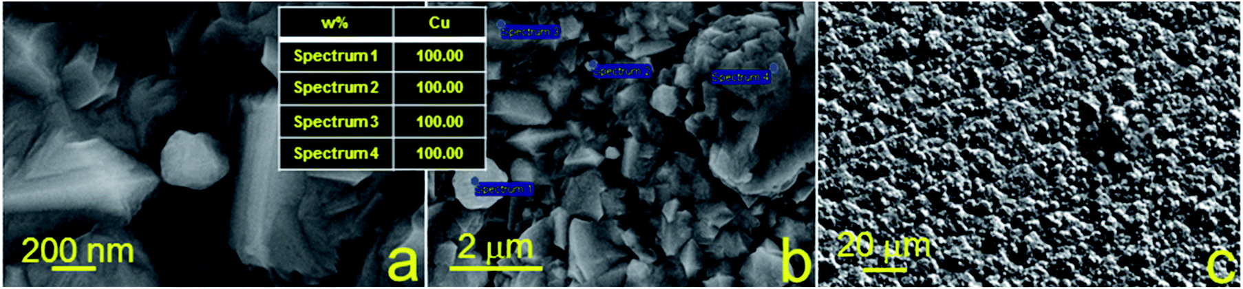 | ||
| Fig. 5 SEM images and EDX analysis of copper structures fabricated using SSAIL on the surface of glass-ceramics. | ||
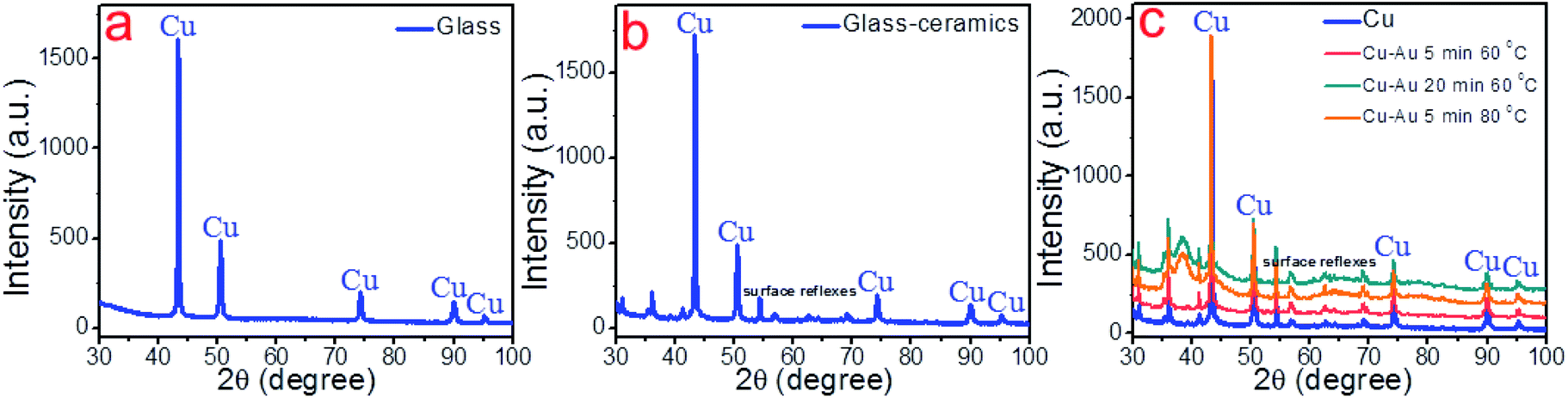 | ||
| Fig. 6 XRD patterns of copper structures fabricated using SSAIL on the surface of (a) glass and (b) glass-ceramics. (c) XRD patterns of copper–gold structures fabricated using SSAIL on the surface of glass-ceramics. | ||
From literature, it is known that electrochemical characteristics of copper-based structures (electrodes) towards enzyme-less sensing can be significantly improved by their modification with noble metals, which exhibit high electrocatalytic activity and have biocompatible nature.9,21,44 As a result, in the current work, we also modified the synthesised copper structures by gold nanoparticles (AuNPs) for the same purpose. The method for template-free grows of AuNW was developed based on procedures published in.45,46 DMAP45 was used as shape-directing agent, where Au deposition proceeded as galvanic replacement reaction, which consisted of a redox process between Cu electrode, serving as a sacrificial template, and AuCl4 ions in solution. Liu et al.46 have reported that copper tends to form Cu–Au alloys with branched structure HAuCl4:
| Cu + Au3+ → Cu2+ + Au(alloy) |
The optimal conditions for the synthesis of bimetallic Cu–Au electrode materials for non-enzymatic sensing are presented in Fig. 7. The results of SEM, EDX and XRD studies are shown in Fig. 8 and 6c, respectively. XRD patterns of Cu–Au electrodes does not reveal any reflexes of crystal Au. However, EDX mapping (Fig. 8) shows the presence of 6% of Au (or more depending on synthesis conditions).
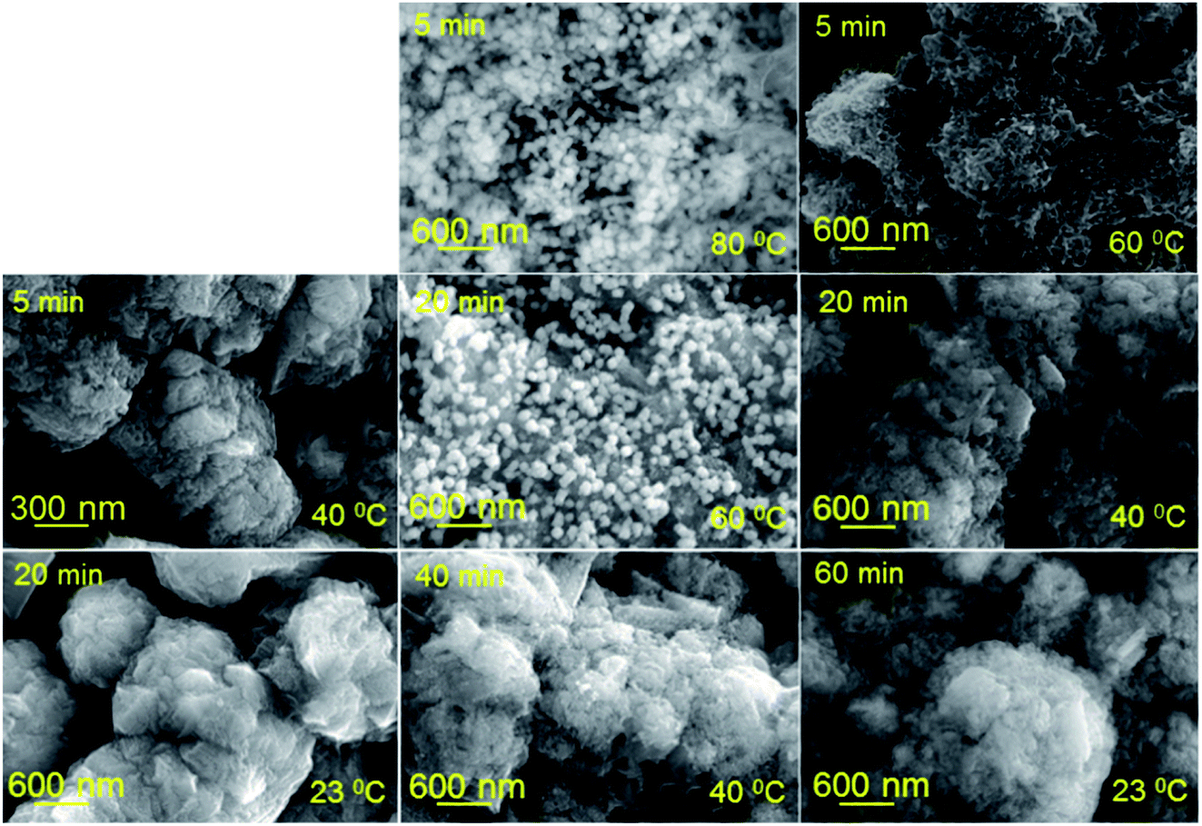 | ||
| Fig. 7 SEM images of copper nanostructures exposed in HAuCl4–DMAP–H2O solution for different time periods at various temperatures. | ||
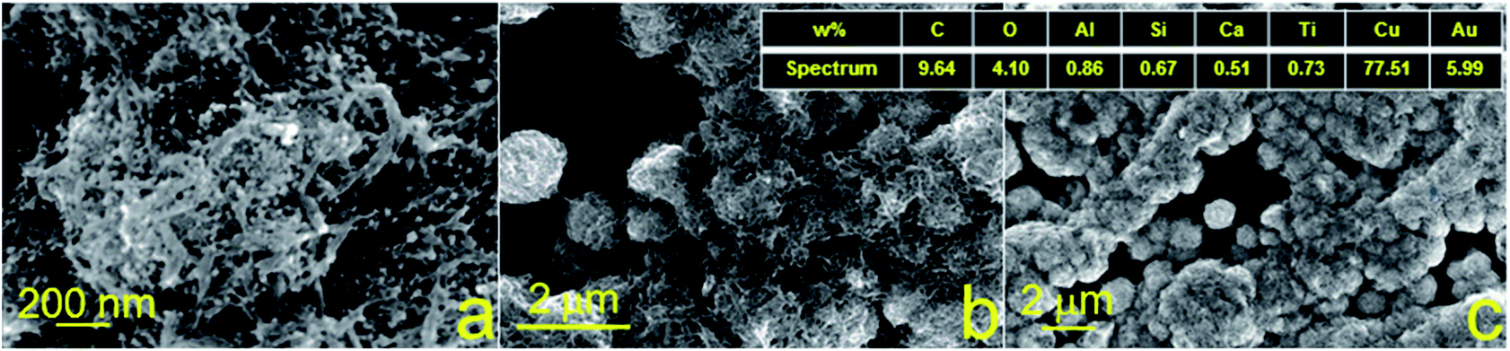 | ||
| Fig. 8 SEM images and EDX analysis of copper–gold structures on the surface of glass-ceramics. | ||
The electrocatalytic activity of the fabricated copper and copper–gold electrodes concerning non-enzymatic sensing of glucose was tested using voltammetric methods. Fig. 9a, 10a and 11a demonstrate cyclic voltammograms (CVs) of these materials measured in the background and D-glucose solutions of various concentrations. The shape of these CVs is similar and has an extensive range of potentials between 0.3 and 0.7 V corresponding to anodic glucose oxidation. The sensitivity of an electrode is a rather important parameter that could be estimated by calculating the area of a CV. As a result, the calculated sensitivities towards glucose detection for copper on glass and glass-ceramics are 719 and 911 μA mM−1 cm−2, respectively. On the other hand, the calculated sensitivity towards glucose detection for copper–gold on glass-ceramics are 3060 μA mM−1 cm−2 (Table 3).
 | ||
| Fig. 9 Electrochemical studies of copper structures on glass: (a) cyclic voltammograms (CVs) recorded in 0.1 M NaOH at different D-glucose concentrations; (b) Amperogram obtained in 0.1 M NaOH with different concentration of D-glucose at the potential of 0.50 V; (c) linear dependence of the measured Faraday current on the D-glucose concentrations; (d) amperometric response to successive addition of 100 μM D-glucose (Glu), 20 μM uric acid (UA), 20 μM ascorbic acid (AA) and 20 μM 4-acetamidophenol (AP) in 0.1 M NaOH. | ||
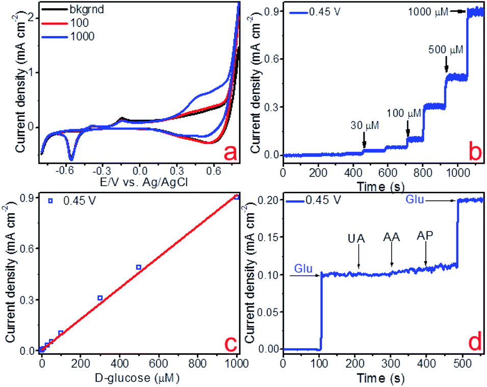 | ||
| Fig. 10 Electrochemical studies of copper structures on glass-ceramics: (a) cyclic voltammograms (CVs) recorded in 0.1 M NaOH at different D-glucose concentrations; (b) amperogram obtained in 0.1 M NaOH with different concentration of D-glucose at the potential of 0.45 V; (c) linear dependence of the measured Faraday current on the D-glucose concentrations; (d) amperometric response to successive addition of 100 μM D-glucose (Glu), 20 μM uric acid (UA), 20 μM ascorbic acid (AA) and 20 μM 4-acetamidophenol (AP) in 0.1 M NaOH. | ||
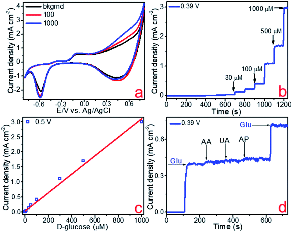 | ||
| Fig. 11 Electrochemical studies of copper–gold structures on glass-ceramics: (a) cyclic voltammograms (CVs) recorded in 0.1 M NaOH at different D-glucose concentrations; (b) amperogram obtained in 0.1 M NaOH with different concentration of D-glucose at the potential of 0.39 V; (c) linear dependence of the measured Faraday current on the D-glucose concentrations; (d) amperometric response to successive addition of 100 μM D-glucose (Glu), 20 μM uric acid (UA), 20 μM ascorbic acid (AA) and 20 μM 4-acetamidophenol (AP) in 0.1 M NaOH. | ||
| Electrode material | Sensitivity (μA mM−1 cm−2) | Linear range (μM) | Limit of detection (μM) | Ref. |
|---|---|---|---|---|
| Cu on glass | 719 | 10–1000 | 1.97 | This work |
| Cu on glass-ceramics | 911 | 3–1000 | 0.75 | This work |
| Cu–Au on glass-ceramics | 3060 | 0.3–1000 | 0.06 | This work |
| Cu coating | 2149.1 | 1–4600 | 0.03 | 47 |
| Cu microparticle | 2432 | 0–4711 | 0.19 | 48 |
| Cu NP | 412 | 0–700 | 2.76 | 49 |
| Cu thin coating | 3643 | 0–811 | 0.59 | 50 |
| Au NP film | 749.2 | 55.6–13890 |
9 | 51 |
| Pt–Cu nanochain | 135 | 10–17000 |
2.5 | 52 |
| Pt-nanoporous Au | 145.7 | 500–10000 |
0.6 | 53 |
| CuO porous film | 2900 | 1–2500 | 0.14 | 54 |
Other important electrochemical characteristics such as the limit of detection (LOD), the linear range of glucose detection and selectivity were obtained using amperometry. Fig. 9b, 10b and 11b illustrate the amperometric response to consecutive additions of D-glucose to 0.1 M NaOH at potentials of 0.45, 0.50 and 0.39 V, respectively. Further, the linear dependence of the analytical signal (Faraday current) was plotted vs. D-glucose concentration, for each material (Fig. 9c, 10c and 11c). According to this data, the linear regime of non-enzymatic glucose detection is provided between 10–1000 and 3–1000 μM for copper on glass and glass-ceramics, respectively, whereas for copper–gold linear range lies between 0.3 and 1000 μM (Table 3). In addition, limits of glucose and hydrogen peroxide detection were calculated for all samples as LOD = 3S/b, where S is the standard deviation from linearity and b is the slope of the calibration curve indicated in Fig. 9c, 10c and 11c, and it is equal to 1.97, 0.75 and 0.06 μM for copper on glass and glass-ceramics as well as copper–gold on glass-ceramics, respectively (Table 3).
It is known from the literature9,44 that the active centers throughout the surface of the electrodes based on transition metals and the presence of hydroxyl radicals play a crucial role in the electrooxidation of glucose and many other analytes. In addition, in bimetallic structures containing noble metals, the resulting synergistic effects lead to an increase in the catalytic activity with respect to the electrooxidation of the above-mentioned substances. Therefore, taking into account these facts and already known models, we can propose a mechanism for glucose oxidation on the surface of the materials obtained in this work (Fig. 12).
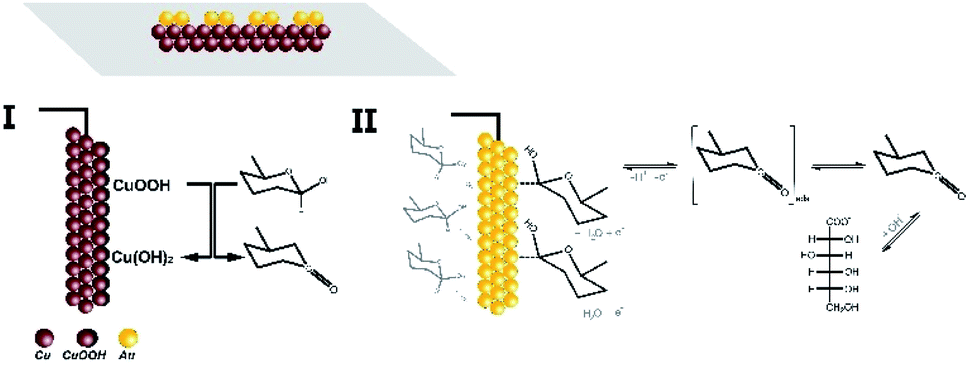 | ||
| Fig. 12 Possible mechanism for electrooxidation of glucose on the surface of copper and copper–gold electrodes. | ||
The selectivity of the fabricated materials towards glucose sensing was tested in the presence of such interfering substances as 4-acetamidophenol (AP), ascorbic acid (AA) and uric acid (UA) that typically coexist with glucose in the human blood (Fig. 9d, 10d and 11d). As a result, copper and copper–gold electrodes have good selectivity for glucose sensing, demonstrating much more significant analytical response towards D-glucose in contrast to other interfering analytes. The long-run stability of copper and copper–gold electrodes was also investigated (Fig. 13). Decent stability was confirmed by testing six samples of each material for 15 days. We observed that during this period, all samples maintained ∼93–96% their initial electrocatalytic activity concerning non-enzymatic glucose sensing.
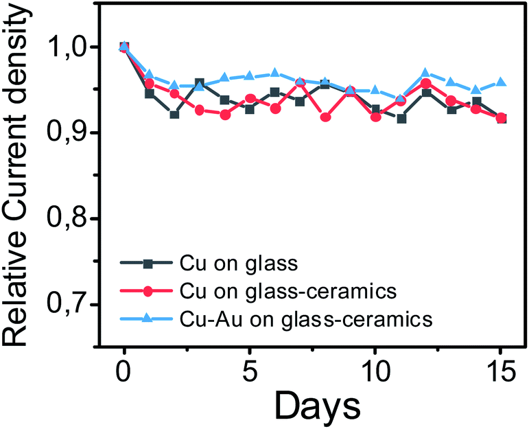 | ||
| Fig. 13 Long-run stability of copper and copper–gold electrodes for non-enzymatic glucose sensing tested during 15 days. | ||
Moreover, the sensor characteristics of copper and copper–gold structures produced by SSAIL were compared with analogical enzyme-less electrodes known from the literature47–54 (Table 3). Thus, one can conclude that SSAIL is a useful and efficient technique for the fabrication of materials suitable enzyme-free sensing of biologically important analytes.
Conclusions
In this work, we used the method of Selective Surface Activation Induced by Laser (SSAIL) to fabricate the electrodes appropriate for enzyme-free glucose determination. This method can afford quick and efficient manufacturing copper electrodes on various dielectric substrates. These electrode materials can easily be modified using nanostructures of such an inert, biologically compatible and catalytically active metal as gold to increase the development of the electrode surface and, as a result, improve its electrochemical characteristics. Thus, we fabricated copper and copper–gold electrodes on the surface of glass and glass-ceramics. We also investigated the electrochemical properties of the obtained materials using voltammetry methods. It was found that the modification of the copper surface with gold nanoparticles can significantly increase the sensitivity of the electrode towards dopamine sensing (3060 vs. 911 μA mM−1 cm−2 for copper on glass-ceramics), improve the detection limit and expand the linear range of detection of this analyte. Besides, the fabricated copper and copper–gold sensor platforms have good selectivity and excellent stability. Thus, SSAIL is a promising high-performance approach to develop new sensors for the enzyme-free detection of various important bioanalytes both in model systems and in the human blood.Conflicts of interest
There are no conflicts to declare.Acknowledgements
I. I. T., E. M. K. and M. S. P. acknowledge Russian Science Foundation (grant 20-79-10075). The authors would like to thank the SPbSU Nanotechnology Interdisciplinary Centre, Centre for Optical and Laser Materials Research and Centre for X-ray Diffraction Studies.References
- E. Cesewski and B. N. Johnson, Electrochemical biosensors for pathogen detection, Biosens. Bioelectron., 2020, 159, 112214 CrossRef CAS PubMed.
- J. Y. Sun, Y. Shi, X. Y. Cai and J. Liu, Potential diagnostic and therapeutic value of circular RNAs in cardiovascular diseases, Cell. Signalling, 2020, 71, 109604 CrossRef CAS PubMed.
- E. Bakker, Electrochemical sensors, Anal. Chem., 2004, 76, 3285–3298 CrossRef CAS PubMed.
- E. Sehit and Z. Altintas, Significance of nanomaterials in electrochemical glucose sensors: An updated review (2016-2020), Biosens. Bioelectron., 2020, 159, 112165 CrossRef CAS PubMed.
- C. Revathi and R. T. Rajendra Kumar, Enzymatic and nonenzymatic electrochemical biosensors, Elsevier Ltd, 2019 Search PubMed.
- A. A. Saei, J. E. N. Dolatabadi, P. Najafi-Marandi, A. Abhari and M. de la Guardia, Electrochemical biosensors for glucose based on metal nanoparticles, TrAC, Trends Anal. Chem., 2013, 42, 216–227 CrossRef CAS.
- S. Ferri, K. Kojima and K. Sode, Review of glucose oxidases and glucose dehydrogenases: A bird's eye view of glucose sensing enzymes, J. Diabetes Sci. Technol., 2011, 5, 1068–1076 CrossRef PubMed.
- S. Nasiri and M. R. Khosravani, Progress and challenges in fabrication of wearable sensors for health monitoring, Sens. Actuators, A, 2020, 312, 112105 CrossRef CAS.
- D. W. Hwang, S. Lee, M. Seo and T. D. Chung, Recent advances in electrochemical non-enzymatic glucose sensors – A review, Anal. Chim. Acta, 2018, 1033, 1–34 CrossRef CAS PubMed.
- X. Liu, W. Yang, L. Chen and J. Jia, Three-Dimensional Copper Foam Supported CuO Nanowire Arrays: An Efficient Non-enzymatic Glucose Sensor, Electrochim. Acta, 2017, 235, 519–526 CrossRef CAS.
- S. Fu, C. Zhu, J. Song, M. Engelhard, H. Xia, D. Du and Y. Lin, PdCuPt Nanocrystals with Multibranches for Enzyme-Free Glucose Detection, ACS Appl. Mater. Interfaces, 2016, 8, 22196–22200 CrossRef CAS PubMed.
- X. Wang, C.-y. Ge, K. Chen and Y. X. Zhang, An ultrasensitive non-enzymatic glucose sensors based on controlled petal-like CuO nanostructure, Electrochim. Acta, 2018, 259, 225–232 CrossRef CAS.
- M. S. Panov, I. I. Tumkin, V. S. Mironov, E. M. Khairullina, A. V. Smikhovskaia, S. S. Ermakov and V. A. Kochemirovsky, Sensory properties of copper microstructures deposited from water-based solution upon laser irradiation at 532 nm, Opt. Quantum Electron., 2016, 48(11) DOI:10.1007/s11082-016-0758-9.
- M. S. Panov, I. I. Tumkin, A. V. Smikhovskaia, E. M. Khairullina, D. I. Gordeychuk and V. A. Kochemirovsky, High rate in situ laser-induced synthesis of copper nanostructures performed from solutions containing potassium bromate and ethanol, Microelectron. Eng., 2016, 157, 13–18 CrossRef CAS.
- V. S. Andriianov, V. S. Mironov, A. V. Smikhovskaia, E. M. Khairullina and I. I. Tumkin, Laser-induced synthesis of carbon-based electrode materials for non-enzymatic glucose detection, Opt. Quantum Electron., 2020, 52, 1–8 CrossRef.
- A. V. Smikhovskaia, M. S. Panov, I. I. Tumkin, E. M. Khairullina, S. S. Ermakov, I. A. Balova, M. N. Ryazantsev and V. A. Kochemirovsky, In situ laser-induced codeposition of copper and different metals for fabrication of microcomposite sensor-active materials, Anal. Chim. Acta, 2018, 1044, 138–146 CrossRef CAS PubMed.
- C. Xu, Y. Liu, F. Su, A. Liu and H. Qiu, Nanoporous PtAg and PtCu alloys with hollow ligaments for enhanced electrocatalysis and glucose biosensing, Biosens. Bioelectron., 2011, 27, 160–166 CrossRef CAS PubMed.
- H. Gao, F. Xiao, C. B. Ching and H. Duan, One-step electrochemical synthesis of PtNi nanoparticle-graphene nanocomposites for nonenzymatic amperometric glucose detection, ACS Appl. Mater. Interfaces, 2011, 3, 3049–3057 CrossRef CAS PubMed.
- M. S. Panov, E. M. Khairullina, F. S. Vshivtcev, M. N. Ryazantsev and I. I. Tumkin, Laser-Induced Synthesis of Composite Materials Based on Iridium, Gold and Platinum for Non-Enzymatic Glucose Sensing, Materials, 2020, 13, 3359 CrossRef CAS PubMed.
- L. Wang, W. Zhu, W. Lu, X. Qin and X. Xu, Surface plasmon aided high sensitive non-enzymatic glucose sensor using Au/NiAu multilayered nanowire arrays, Biosens. Bioelectron., 2018, 111, 41–46 CrossRef CAS PubMed.
- M. S. Panov, O. A. Vereshchagina, S. S. Ermakov, I. I. Tumkin, E. M. Khairullina, M. Y. Skripkin, A. S. Mereshchenko, M. N. Ryazantsev and V. A. Kochemirovsky, Non-enzymatic sensors based on in situ laser-induced synthesis of copper–gold and gold nano-sized microstructures, Talanta, 2017, 167, 201–207 CrossRef CAS PubMed.
- M. Panov, I. Aliabev, E. Khairullina, V. Mironov and I. Tumkin, Fabrication of nickel-gold microsensor using in situ laser-induced metal deposition technique, J. Laser Micro/Nanoeng., 2019, 14, 266 CAS.
- A. V. Smikhovskaia, V. S. Andrianov, E. M. Khairullina, D. V. Lebedev, M. N. Ryazantsev, M. S. Panov and I. I. Tumkin, In situ laser-induced synthesis of copper-silver microcomposite for enzyme-free D-glucose and L-alanine sensing, Appl. Surf. Sci., 2019, 488, 531–536 CrossRef CAS.
- C. H. Su, C. W. Kung, T. H. Chang, H. C. Lu, K. C. Ho and Y. C. Liao, Inkjet-printed porphyrinic metal–organic framework thin films for electrocatalysis, J. Mater. Chem. A, 2016, 4, 11094–11102 RSC.
- M. Li, Y. T. Li, D. W. Li and Y. T. Long, Recent developments and applications of screen-printed electrodes in environmental assays-A review, Anal. Chim. Acta, 2012, 734, 31–44 CrossRef CAS PubMed.
- M. Bariya, Z. Shahpar, H. Park, J. Sun, Y. Jung, W. Gao, H. Y. Y. Nyein, T. S. Liaw, L. C. Tai, Q. P. Ngo, M. Chao, Y. Zhao, M. Hettick, G. Cho and A. Javey, Roll-to-Roll Gravure Printed Electrochemical Sensors for Wearable and Medical Devices, ACS Nano, 2018, 12, 6978–6987 CrossRef CAS PubMed.
- D. Barreca, C. Massignan, S. Daolio, M. Fabrizio, C. Piccirillo, L. Armelao and E. Tondello, Composition and microstructure of cobalt oxide thin films obtained from a novel cobalt(II) precursor by chemical vapor deposition, Chem. Mater., 2001, 13, 588–593 CrossRef CAS.
- M. Li, H. Wang, X. Wang, Q. Lu, H. Li, Y. Zhang and S. Yao, Ti3C2/Cu2O heterostructure based signal-off photoelectrochemical sensor for high sensitivity detection of glucose, Biosens. Bioelectron., 2019, 142, 111535 CrossRef CAS PubMed.
- M. Jalali, R. S. Moakhar, T. Abdelfattah, E. Filine, S. S. Mahshid and S. Mahshid, Nanopattern-Assisted Direct Growth of Peony-like 3D MoS2/Au Composite for Nonenzymatic Photoelectrochemical Sensing, ACS Appl. Mater. Interfaces, 2020, 12, 7411–7422 CrossRef CAS PubMed.
- V. E. Baranauskaite, M. O. Novomlinskii, I. I. Tumkin, E. M. Khairullina, A. S. Mereshchenko, I. A. Balova, M. S. Panov and V. A. Kochemirovsky, In situ laser-induced synthesis of gas sensing microcomposites based on molybdenum and its oxides, Composites, Part B, 2019, 157, 322–330 CrossRef CAS.
- V. A. Kochemirovsky, M. Y. Skripkin, Y. S. Tveryanovich, A. S. Mereshchenko, A. O. Gorbunov, M. S. Panov, I. I. Tumkin and S. V. Safonov, Laser-induced copper deposition from aqueous and aqueous–organic solutions: state of the art and prospects of research, Russ. Chem. Rev., 2015, 84, 1059–1075 CrossRef CAS.
- L. S. Logunov, M. S. Panov, L. A. Myund, I. I. Tumkin, E. M. Khairullina, M. N. Ryazantsev, I. A. Balova and V. A. Kochemirovsky, Influence of the ligand nature on the in situ laser-induced synthesis of the electrocatalytically active copper microstructures, Arabian J. Chem., 2018, 11, 624–634 CrossRef CAS.
- G. Li, Direct laser writing of graphene electrodes, J. Appl. Phys., 2020, 127, 8725–8729 Search PubMed.
- S. Papazoglou and I. Zergioti, Laser Induced Forward Transfer (LIFT) of nano-micro patterns for sensor applications, Microelectron. Eng., 2017, 182, 25–34 CrossRef CAS.
- M. Mizoshiri, S. Arakane, J. Sakurai and S. Hata, Direct writing of Cu-based micro-temperature detectors using femtosecond laser reduction of CuO nanoparticles, Appl. Phys. Express, 2016, 9 DOI:10.7567/APEX.9.036701.
- V. B. Nam, J. Shin, Y. Yoon, T. T. Giang, J. Kwon, Y. D. Suh, J. Yeo, S. Hong, S. H. Ko and D. Lee, Highly Stable Ni-Based Flexible Transparent Conducting Panels Fabricated by Laser Digital Patterning, Adv. Funct. Mater., 2019, 29, 1–10 Search PubMed.
- B. Kang, S. Han, J. Kim, S. Ko and M. Yang, One-step fabrication of copper electrode by laser-induced direct local reduction and agglomeration of copper oxide nanoparticle, J. Phys. Chem. C, 2011, 115, 23664–23670 CrossRef CAS.
- D. Chen, Q. Lu and Y. Zhao, Laser-induced site-selective silver seeding on polyimide for electroless copper plating, Appl. Surf. Sci., 2006, 253, 1573–1580 CrossRef CAS.
- M. Huske, J. Kickelhain, J. Muller and G. Eber, Laser supported activation and additive metallization of thermoplastics for 3D-MIDs, Proc. LANE, 2001, 3, 587–598 Search PubMed.
- O. Koritsoglou, I. Theodorakos, F. Zacharatos, M. Makrygianni, D. Kariyapperuma, R. Price, B. Cobb, S. Melamed, A. Kabla, F. de la Vega and I. Zergioti, Copper micro-electrode fabrication using laser printing and laser sintering processes for on-chip antennas on flexible integrated circuits, Opt. Mater. Express, 2019, 9, 3046 CrossRef CAS.
- K. Ratautas, M. Andrulevičius, A. Jagminienė, I. Stankevičienė, E. Norkus and G. Račiukaitis, Laser-assisted selective copper deposition on commercial PA6 by catalytic electroless plating – Process and activation mechanism, Appl. Surf. Sci., 2019, 470, 405–410 CrossRef CAS.
- K. Ratautas, A. Jagminienė, I. Stankevičienė, M. Sadauskas, E. Norkus and G. Račiukaitis, Evaluation and optimisation of the SSAIL method for laser-assisted selective electroless copper deposition on dielectrics, Results Phys., 2020, 16 DOI:10.1016/j.rinp.2020.102943.
- K. Ratautas, V. Vosylius, A. Jagminienė, I. Stankevičienė, E. Norkus and G. Račiukaitis, Laser-induced selective electroless plating on pc/abs polymer: Minimisation of thermal effects for supreme processing speed, Polymers, 2020, 12, 1–16 CrossRef PubMed.
- K. E. Toghill and R. G. Compton, Electrochemical non-enzymatic glucose sensors: A perspective and an evaluation, Int. J. Electrochem. Sci., 2010, 5, 1246–1301 CAS.
- F. Muench, S. Schaefer, L. Hagelüken, L. Molina-Luna, M. Duerrschnabel, H. J. Kleebe, J. Brötz, A. Vaskevich, I. Rubinstein and W. Ensinger, Template-Free Electroless Plating of Gold Nanowires: Direct Surface Functionalization with Shape-Selective Nanostructures for Electrochemical Applications, ACS Appl. Mater. Interfaces, 2017, 9, 31142–31152 CrossRef CAS PubMed.
- Y. Liu and A. R. Hight Walker, Preferential outward diffusion of Cu during unconventional galvanic replacement reactions between HAuCl4 and surface-limited Cu nanocrystals, ACS Nano, 2011, 5, 6843–6854 CrossRef CAS PubMed.
- L. Hou, H. Zhao, S. Bi, Y. Xu and Y. Lu, Ultrasensitive and highly selective sandpaper-supported copper framework for non-enzymatic glucose sensor, Electrochim. Acta, 2017, 248, 281–291 CrossRef CAS.
- M. M. Guo, Y. Xia, W. Huang and Z. Li, Electrochemical fabrication of stalactite-like copper micropillar arrays via surface rebuilding for ultrasensitive nonenzymatic sensing of glucose, Electrochim. Acta, 2015, 151, 340–346 CrossRef CAS.
- L. Shi, X. Zhu, T. Liu, H. Zhao and M. Lan, Encapsulating Cu nanoparticles into metal–organic frameworks for nonenzymatic glucose sensing, Sens. Actuators, B, 2016, 227, 583–590 CrossRef CAS.
- M. M. Guo, P. S. Wang, C. H. Zhou, Y. Xia, W. Huang and Z. Li, An ultrasensitive non-enzymatic amperometric glucose sensor based on a Cu-coated nanoporous gold film involving co-mediating, Sens. Actuators, B, 2014, 203, 388–395 CrossRef CAS.
- C. W. Hsu, F. C. Su, P. Y. Peng, H. T. Young, S. Liao and G. J. Wang, Highly sensitive non-enzymatic electrochemical glucose biosensor using a photolithography fabricated micro/nano hybrid structured electrode, Sens. Actuators, B, 2016, 230, 559–565 CrossRef CAS.
- X. Cao, N. Wang, S. Jia and Y. Shao, Detection of glucose based on bimetallic PtCu nanochains modified electrodes, Anal. Chem., 2013, 85, 5040–5046 CrossRef CAS PubMed.
- H. Qiu and X. Huang, Effects of Pt decoration on the electrocatalytic activity of nanoporous gold electrode toward glucose and its potential application for constructing a nonenzymatic glucose sensor, J. Electroanal. Chem., 2010, 643, 39–45 CrossRef CAS.
- S. Cherevko and C. H. Chung, The porous CuO electrode fabricated by hydrogen bubble evolution and its application to highly sensitive non-enzymatic glucose detection, Talanta, 2010, 80, 1371–1377 CrossRef CAS PubMed.
| This journal is © The Royal Society of Chemistry 2021 |