
 Open Access Article
 This Open Access Article is licensed under a Creative Commons Attribution-Non Commercial 3.0 Unported Licence
Effect of the number of nitrogen dopants on the electronic and magnetic properties of graphitic and pyridinic N-doped graphene – a density-functional study
Erik Bhekti Yutomo ,
Fatimah Arofiati Noor* and
Toto Winata
,
Fatimah Arofiati Noor* and
Toto Winata
Physics of Electronics Materials Research Division, Department of Physics, Faculty of Mathematics and Natural Sciences, InstitutTeknologi Bandung, Bandung 40132, Indonesia. E-mail: erikbhektiyutomo@gmail.com; fatimah@fi.itb.ac.id; toto@fi.itb.ac.id
First published on 21st May 2021
Abstract
Doping with nitrogen atom is an effective way to modify the electronic and magnetic properties of graphene. In this paper, we studied the effect of the number of dopant atoms on the electronic and magnetic properties of the two most common nitrogen bond configurations in N-doped graphene, that is, graphitic and pyridinic, using density functional theory (DFT). We found that the formation of graphitic and pyridinic configurations can initiate the transition of the electronic properties of graphene from semimetal to metal with n-type conductivity for the graphitic configuration and p-type conductivity for the pyridinic configuration. The formation of a bandgap-like structure was observed in both configurations. The bandgap increased with the increase in the number of dopant atoms. We also observed that the formation of graphitic configuration did not cause a transition to the magnetic properties of graphene even though the number of dopant atoms was increased. In the pyridinic configuration, the increase in the number of dopant atoms caused graphene to be paramagnetic, with the remarkable total magnetic moment of 0.400 μB per cell in the pyridinic-N3 model. This study provides a deeper understanding of the modification of electronic and magnetic properties of N-doped graphene by controlling the bond configuration and the number of nitrogen dopants.
1. Introduction
Low-dimensional materials, especially in 2D forms such as graphene, transition metal dichalcogenides, metal chalcogenide, hexagonal boron nitride, and silicene, have attracted both experimental and theoretical interest because of their unique structure and electronic properties.1–3 The properties differ significantly from those of the parent compound, owing to quantum confinement and lattice symmetry changes.4,5 Among these materials, the 2D material graphene has superior electronic and mechanical properties.6–8 The combination of high carrier mobility and robust structure makes graphene a promising candidate for many potentials applications, such as nanoelectronic and spintronic devices.9,10 However, the absence of a bandgap limits the application of graphene in nanoelectronics to those allowing for high on–off ratios, such as a field-effect transistor (FET) and integrated circuit (IC).11–13 Furthermore, pristine graphene is nonmagnetic because of its delocalized π bonds, limiting its application in spintronics.14 To expand the application of graphene-based electronic devices, the modulation of the electronic and magnetic properties of graphene is necessary.Many methods have been proposed to modulate the electronic and magnetic properties of graphene, such as creating nanoribbon structures, controlling edge geometry, incorporating covalent or noncovalent functionalization, and doping with foreign atoms.15–19 Among these methods, doping is the most feasible for opening the bandgap and initiating magnetic phase transitions. Nitrogen is the most commonly used dopant because its covalent radius is similar to carbon but with one extra electron.14,18,20 Nitrogen-doped graphene can be synthesized through several methods, such as chemical vapor deposition (CVD), using CH4 as a carbon source and NH3 as a nitrogen source, and mechanical exfoliation of graphene oxide (GO) followed by the addition of hydrazine hydrate as a nitrogen source.21,22 In a graphene lattice, nitrogen can form three types of bond configurations (graphitic, pyridinic, and pyrrolic) depending on the synthesis parameters (e.g., temperature, method, and nitrogen source).14,20,23 In the graphitic configuration, nitrogen atoms substitute carbon atoms in the graphene lattice through sp2 hybridization. Then, the pyridinic configuration is created when the carbon atom has a single vacancy, and the nitrogen atom substitutes the carbon atom near the vacancy site, forming sp2 hybridization. Finally, the pyrrolic formation is created when graphene has a double vacancy; then, the nitrogen atom, together with the carbon atom, forms a pentagonal ring bond. In the pyrrolic configuration, the nitrogen atoms undergo sp3 hybridization. Experimentally, the three atomic nitrogen configurations can be distinguished easily using X-ray photoelectron spectroscopy (XPS) and analyzing the binding energies of the N 1s peaks.14,24
Several studies have shown that different bond configurations can significantly affect the electronic and magnetic properties of graphene. For example, Jalili et al.25 studied the effect of nitrogen–dopant bond configuration on graphene electronic properties using the density functional theory (DFT) method and found a change in conductivity behavior where graphitic N-doped graphene has n-type conductivity, but pyridinic and pyrrolic N-doped graphene have p-type conductivity. Ma et al.26 used the DFT method and found that pristine graphene and graphitic N-doped graphene are nonmagnetic. However, pyridinic and pyrrolic N-doped graphene have spin polarization with magnetic moments of 0.54 and 0.95 μB. The unpaired electrons and the π bond play an essential role in modifying the magnetic properties of graphene. In addition to the bond configuration, the number of dopant atoms also affects the physical properties of graphene. Zhang et al.27 and Olaniyan et al.28 reported that increasing the dopant atoms in the graphitic N-doped graphene can increase the opening of graphene Dirac cones and the Fermi shift towards the conduction band.
Among these, the formation of graphitic and pyridinic configurations can potentially improve the physical properties of graphene. Moreover, graphitic and pyridinic nitrogen are the most thermodynamically stable bond configurations in the graphene lattice.29,30 Zhang et al.31 applied the DFT method to analyze the effect of the nitrogen bonding configuration on the capacitance properties of graphene. They found that the formation of graphitic and pyridinic configurations can increase total capacitance by increasing quantum capacitance. In contrast, the formation of pyrrolic configurations decreases total capacitance because of their low quantum capacitance. Faisal et al.32 supported this finding and succeeded in increasing the capacitance properties of graphene by synthesizing pyridinic and graphitic nitrogen-rich graphene. The sample had a capacitance of 230 F g−1 at a current density of 1 A g−1 and a remarkable high energy density of 62.6 W h kg−1, making it suitable for supercapacitor electrodes. Furthermore, Lin et al.18 synthesized graphitic N-doped graphene with remarkable carrier mobility of 13![[thin space (1/6-em)]](https://www.rsc.org/images/entities/char_2009.gif) 000 cm2 (V s)−1 and reduced sheet resistance down to 130 Ω sq.−1.
000 cm2 (V s)−1 and reduced sheet resistance down to 130 Ω sq.−1.
However, no reports assess the effect of the number of dopant atoms in graphitic dan pyridinic configuration on the modulation of the electronic and magnetic properties of graphene. Previous reports have only focused on the effect of the number of dopant atoms on the electronic properties of graphitic N-doped graphene. In this research, we systematically studied the electronic and magnetic properties of nitrogen-doped graphene with graphitic and pyridinic configurations at different numbers of dopant atoms. We also discuss the structural properties of each model for a better understanding.
2. Computational methodology
In this study, graphitic N-doped graphene and pyridinic N-doped graphene were modeled by 4 × 4 supercell graphene, consisting of 32 carbon atoms. The carbon atom was substituted directly with the nitrogen (N) atom to obtain the graphitic configuration.20,33 While in the pyridinic configuration, one carbon atom was removed first to make a vacancy, then the carbon atom near the vacancy site was substituted with an N atom.20,33 The schematic of the formation of graphitic and pyridinic nitrogen configurations is shown in Fig. 1. In this study, we used three variations in the number of dopant atoms – graphitic-N, graphitic-N2, and graphitic-N3 refer to the graphene doped by one, two, and three nitrogen atoms, respectively, forming the graphitic configurations. Furthermore, pyridinic-N, pyridinic-N2, and pyridinic-N3 represent the graphene doped by one, two, and three nitrogen atoms, respectively, forming pyridinic configurations.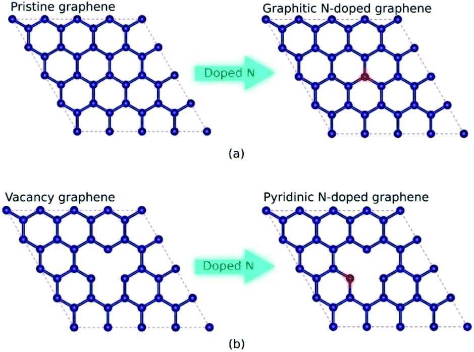 | ||
| Fig. 1 The schematic of the formation of (a) graphitic and (b) pyridinic bond configurations with one dopant atom in an N-doped graphene system (the red balls denote N atoms, and the blue balls denote C atoms). The nitrogen atom directly substitutes for a carbon atom in the graphitic configuration. In contrast, in the pyridinic configuration, the binding of the nitrogen atom in the graphene lattice is assisted by a single vacancy. | ||
The calculations of structural, electronic, and magnetic properties were carried out using the Quantum ESPRESSO code based on the DFT method.34,35 The projector-augmented-wave (PAW) method was used to treat valence electron configurations.36 The exchange–correlation interaction was approximated by generalized gradient approximation (GGA) based on the Perdew–Burke–Ernzerhof (PBE) functional.37 In previous research, the GGA-PBE functional has successfully described the electronic properties of carbon-based materials.38,39 A vacuum of 10 Å along the z-axis was used to avoid interactions between the closest graphene layers. A k-point mesh of 7 × 7 × 1, an energy cut-off of ∼816 eV, a threshold energy of ∼13.6 meV, and a threshold force of ∼25 meV Å−1 were the parameters in the SCF calculation. The band structure calculation was carried out through the Γ–K–M–Γ path in the irreducible Brillouin zone. The non-self-consistent field (NSCF) calculation was performed using the same parameters when calculating the SCF. However, the number of k-points mesh doubled to 14 × 14 × 1, which was suitable for calculating the spin-polarized density of state (SPDOS). Before calculating the structural, electronic, and magnetic properties, the lattice parameters and atomic positions were fully optimized using a vc-relax calculation with the Broyden–Fletcher–Goldfarb–Shanno (BFGS) algorithm.40–43
We also calculated defect formation energies ΔE according to eqn (2). The defect formation energy is a parameter that expresses the stability of the system.44,45
 | (1) |
| ΔE = EC32−x−yNx + (x + y)μC − EC32 − xμN | (2) |
3. Result and discussion
3.1. Structural properties
Table 1 presents the optimized bond lengths and defect formation energies ΔE of all models. The average C–C bond length of pristine graphene is slightly larger than the experimental results (C–C bond length = 1.420 Å).48 However, because the difference is not significant, the result is acceptable. Pristine graphene has a hexagonal lattice with a planar structure, as shown in Fig. 2(a). Furthermore, Fig. 3(a–c) show the optimized geometry of graphitic N-doped graphene with different numbers of dopant atoms. We observed a symmetry breaking of the graphene sub-lattices after a graphitic bond formed. In this study, the magnitude of symmetry breaking was represented by the difference of the maximum and minimum C–C bond length ΔC–C. The ΔC–C value increased with the number of dopant atoms on the graphitic configuration (Table 1), thus increasing the symmetry breaking. The sub-lattice symmetry breaking in the graphitic N-doped graphene was due to nitrogen atoms having smaller covalent radii than carbon atoms (rN = 0.75 Å and rC = 0.77 Å). The same behavior is also observed when graphene is doped by other atoms with different covalent radii, such as B, Al, Si, Ge, As, and Sb.49 The difference in covalent radii between two atoms in a unit cell will cause lattice distortion.50 We also observed that the graphitic bonding configuration did not destroy the planar structure of graphene.| Models | ΔE (eV) | Bond length (Å) | |||||||
|---|---|---|---|---|---|---|---|---|---|
| C–C | C–N | ||||||||
| Min | Max | ΔC–C | Average | Min | Max | ΔC–N | Average | ||
| Pristine | — | 1.424 | 1.424 | 0.000 | 1.424 | — | — | — | — |
| Graphitic-N | 0.066 | 1.414 | 1.429 | 0.015 | 1.422 | 1.412 | 1.412 | 0.000 | 1.412 |
| Graphitic-N2 | 0.173 | 1.404 | 1.434 | 0.030 | 1.420 | 1.398 | 1.424 | 0.026 | 1.414 |
| Graphitic-N3 | 0.249 | 1.398 | 1.433 | 0.036 | 1.416 | 1.396 | 1.437 | 0.041 | 1.426 |
| Pyridinic-N | 0.375 | 1.393 | 1.523 | 0.131 | 1.429 | 1.318 | 1.318 | 0.000 | 1.318 |
| Pyridinic-N2 | 0.352 | 1.392 | 1.449 | 0.057 | 1.422 | 1.334 | 1.362 | 0.028 | 1.334 |
| Pyridinic-N3 | 0.258 | 1.415 | 1.452 | 0.037 | 1.431 | 1.340 | 1.340 | 0.000 | 1.340 |
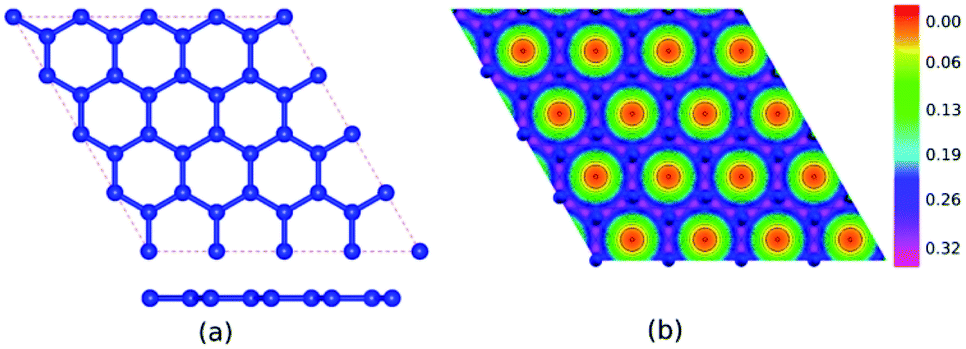 | ||
| Fig. 2 (a) Optimized geometry and (b) electron density of pristine graphene. | ||
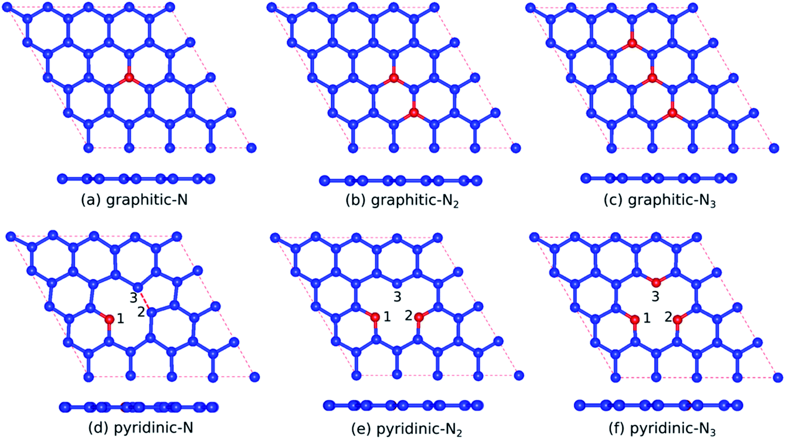 | ||
| Fig. 3 Optimized geometry of (a) graphitic-N, (b) graphitic-N2, (c) graphitic-N3, (d) pyridinic-N, (e) pyridinic-N2, and (f) pyridinic-N3 models (the red balls denote N atoms, and the blue balls denote C atoms). | ||
However, in the pyridinic configuration, the symmetry breaking of the graphene sub-lattice decreased when the number of dopant atoms increased, which was indicated by a decreasing ΔC–C (Table 1). The pyridinic-N model has the greatest symmetry breaking because of the weak covalent bond between unpaired electrons of the C2 and C3 atoms. Therefore, the two atoms moved closer to each other, producing a distance between C2 and C3 atoms of 1.7 Å, as shown in Fig. 3(d). This interaction caused the formation of a pentagonal ring, initiating the Jahn–Teller distortion.51 Wu et al.52 also observed changes in the graphene structure due to the interaction between two carbon atoms around the vacancy site, which resulted in a bond length of 2.17 Å.
Therefore, the presence of nitrogen atoms could strengthen the interaction between the C2 and C3 atoms because of the reduced bond length. The addition of one dopant atom (pyridinic-N2) left one dangling bond in atom C3, as indicated by Fig. 3(e), causing graphene to become more reactive, a suitable feature for gas sensor applications.53 In the pyridinic-N3 model, the symmetry breaking of the graphene sub-lattice decreased because the three carbon atoms closest to the vacancy site, which have unsaturated dangling bonds, were substituted with nitrogen atoms, as presented in Fig. 3(f). Furthermore, as in the graphitic configuration, the formation of the pyridinic bond did not destroy the planar structure of graphene.
In this study, we also observed that the defect formation energy ΔE increased with the magnitude of symmetry breaking. In this way, the model with less symmetry breaking is more energetically favorable. In the graphitic configuration, the model with the smallest number of dopant atoms (graphitic-N) was most energetically favorable. In contrast, a pyridinic configuration with the largest number of dopant atoms (pyridinic-N3) was most energetically favorable. Furthermore, because the defect formation energy in the graphitic configuration was smaller than that in the pyridinic configuration, the graphitic configuration is predicted to be more energetically favorable. These results explain why, in N-doped graphene, growth is always dominated by the formation of a graphitic configuration.21,22
3.2. Electronic properties
Fig. 2(b) shows the electron density of pristine graphene. The red color represents the electron-lack region, and the purple color represents the electron-rich region. In pristine graphene, the electrons are distributed on a hexagonal lattice. This result is consistent with the theory in which each carbon atom in graphene has four valence electrons that undergo sp2 hybridization so that the electrons will be distributed around the C–C bond.7Furthermore, Fig. 4(a–f) shows the electron densities of the graphitic and pyridinic N-doped graphene with different numbers of dopant atoms. The nitrogen dopant caused a decrease in electron density around the carbon atom near the dopant site. More electrons occupied the area around the nitrogen atom, indicating a transfer of electrons from the carbon atom to the nitrogen atom. Charge transfer could occur because nitrogen atoms have a greater electronegativity than carbon atoms (χN = 3.04 and χC = 2.55), and, thus, nitrogen atoms tend to attract electrons when bonding with carbon atoms. Several previous studies have also confirmed the existence of electron transfer when there is a difference in electronegativity between the dopant atom and the carbon atom in the graphene lattice.19,54 In the pyridinic-N model, an increase in electron density was observed in the region between atoms C2 and C3, as shown in Fig. 4(d). This result confirmed the interaction between the unpaired electrons on the carbon atom near the vacancy site.
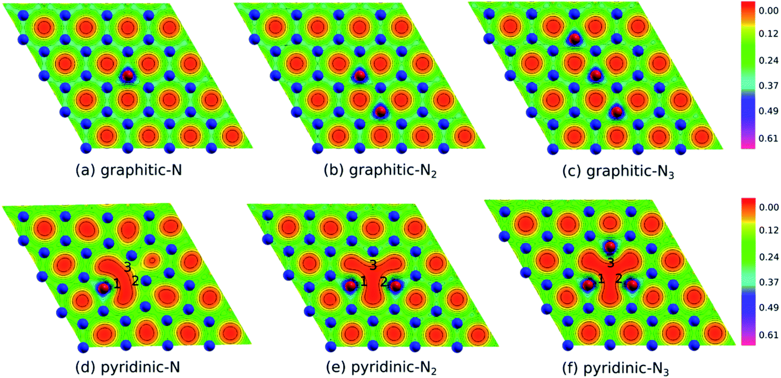 | ||
| Fig. 4 Electron density of (a) graphitic-N, (b) graphitic-N2, (c) graphitic-N3, (d) pyridinic-N, (e) pyridinic-N2, and (f) pyridinic-N3 models. | ||
Fig. 5(a) shows the band structure of pristine graphene, revealing a relatively wide bandgap at the Γ and M points. At the K point, the valence and conduction bands meet at the Fermi energy to form a Dirac point. The combination of semiconductor and conductor behavior classifies graphene as a semimetal. These results are consistent with previous experimental and theoretical studies.7,55 Furthermore, Fig. 6(a–c) shows the band structure of graphitic N-doped graphene with different numbers of dopant atoms. We observed a transition in the electronic properties of graphene from semimetal to metal, indicated by the Fermi level across the conduction band. These results show that the formation of graphitic bond can increase the conductivity of graphene. An increase in conductivity was also observed by Lin et al.18 who reduced N-doped graphene resistance down to 130 Ω sq.−1 by making graphitic bonds dominate the system.
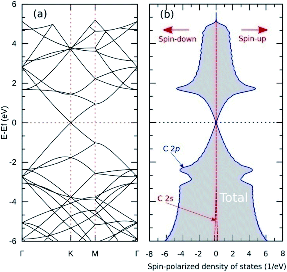 | ||
| Fig. 5 (a) Band structure and (b) SPDOS of pristine graphene. | ||
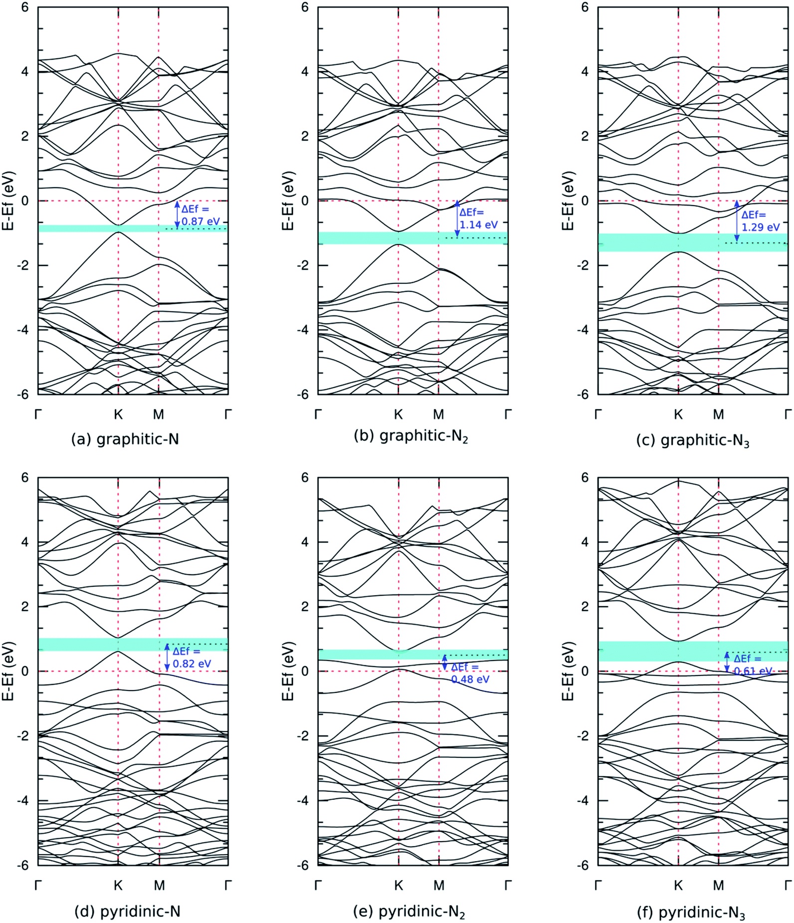 | ||
| Fig. 6 Band structures of (a) graphitic-N, (b) graphitic-N2, (c) graphitic-N3, (d) pyridinic-N, (e) pyridinic-N2, and (f) pyridinic-N3 models. Cyan colored areas denote bandgap, and ΔEf refers to the magnitude of the Fermi level shifting. | ||
In graphitic bonds, the nitrogen atom will undergo sp2 hybridizations where three electrons from the nitrogen atom will form a σ bond with three carbon atoms. One electron will form a π bond with the carbon atom, and the remaining electron will contribute to the formation of the π* donor state in conduction bands. This donor state will cause a shift in Fermi energy towards a higher energy level. Fig. 6(a–c) whos that this shift increased with the number of dopants because the nitrogen atom contributed more donor states. Graphitic N-doped graphene has an n-type conductivity due to additional states in the conduction band.
The formation of graphitic configuration also caused the opening bandgap around the Dirac point. The bandgap increased with the number of dopant atoms, as shown in Table 2. The bandgap's formation is due to the symmetry breaking of the graphene sub-lattice, as explained in the structural properties analysis. The symmetry breaking expanded when the dopant concentration increased and, hence, the bandgap increased. Although basically what was formed is not the actual bandgap, the control of the transport properties of charge carrier in graphene is possible using a gate voltage.52 These results indicate that graphene can be applied as a FET as a semiconductor channel, which generally has an energy gap of 0.4 eV and above.11
The magnitude of the bandgap of the graphitic configuration obtained in this study is consistent with other calculation results (Table 2). Notably, in this study, we only used GGA-PBE functional to treat exchange–correlation interaction, while the calculation conducted by Olaniyan et al.28 used a hybrid/HSE06 functional, which requires a longer calculation time. Next, our results were compared with experimental studies. Usachov et al.56 reported graphitic N-doped graphene with 1–2% dopant concentration has a bandgap of 0.2 eV. These results were used to validate the results obtained in this study.
Fig. 6(d–f) show the band structure of pyridinic N-doped graphene. In this model, we also observed the Fermi level across the valence band, which indicates a transition in the electronic properties of graphene from semimetal to metal. The shift in Fermi levels was caused by a single vacancy that forms in the pyridinic configuration. A single vacancy yields a system that lacks electrons, thus creating an acceptor state in the valence band that pushes the Fermi level downward. The Fermi level shift was reduced as the number of dopant atoms increased, owing to the increased donor state provided by the nitrogen atom. Pyridinic N-doped graphene has p-type conductivity, resulting from the presence of additional states in the valence band. In the pyridinic-N2 and pyridinic-N3 models, we observed a flat band near the Fermi level, which was predicted to come from unsaturated dangling bonds. This flat band is critical to maintaining the stability of the magnetic properties of graphene at high temperatures.57
We also observed an opening bandgap in the pyridinic configuration model due to the symmetry breaking of the graphene sub-lattices (Table 2). Jalili et al.25 obtained a bandgap of the pyridinic-N3 model of 0.500 eV using the LDA functional, but we obtained a slightly larger bandgap because the GGA functional is more accurate in calculating the material bandgap. Pyridinic N-doped graphene has a larger bandgap than graphitic N-doped graphene because the symmetry breaking caused by forming pyridinic bonds is greater (Table 1). These results show that the electronic properties of nitrogen-doped graphene are very flexible and can be controlled by adjusting the bond configuration and the number of dopant atoms.
3.3. Magnetic properties
The analysis of the magnetic properties was carried out by calculating the SPDOS for each model. Fig. 5(b) shows the SPDOS of pristine graphene and the symmetrical behavior between SPDOS of spin-up and spin-down states, indicating that pristine graphene is nonmagnetic. This result is consistent with previous theoretical and experimental studies regarding the magnetic properties of pristine graphene.14 Based on the SPDOS calculations, the hybridization of the C 2s and C 2p orbitals in the C–C bond were evident. Furthermore, Fig. 7(a–c) show the SPDOS for the graphitic configuration. We also observed symmetrical behavior between SPDOS of spin-up and spin-down states for all variations of the number of dopant atoms. This condition indicates that the graphitic N-doped graphene was nonmagnetic even though the number of dopant atoms increased.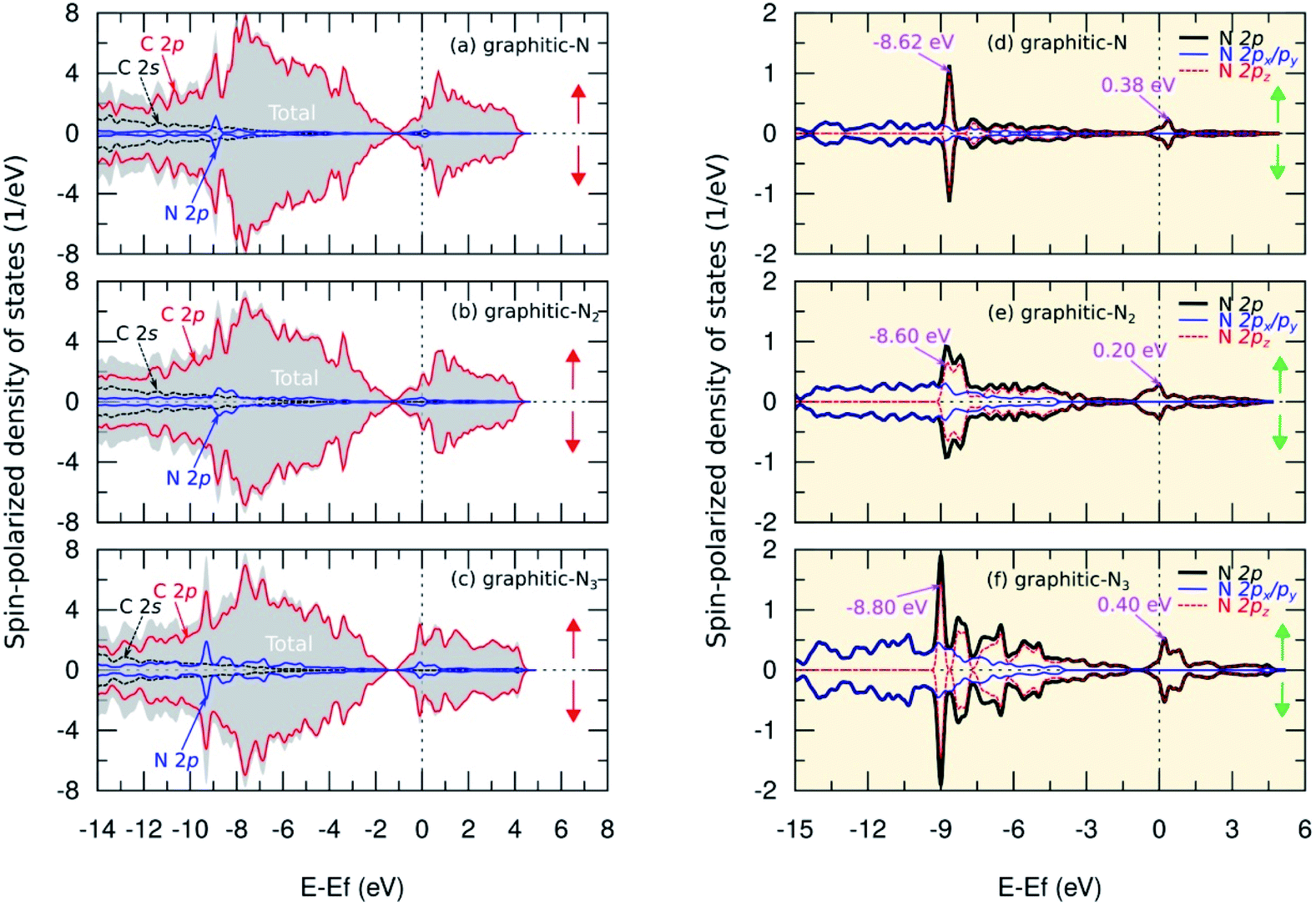 | ||
| Fig. 7 Spin-polarized density of states (SPDOS) of C 2s, C 2p, and N 2p orbitals in (a) graphitic-N, (b) graphitic-N2, and (c) graphitic-N3 models. We also present SPDOS curve of sub-N 2p (px, py, pz) orbitals in (d) graphitic-N, (e) graphitic-N2, and (f) graphitic-N3 models. The spin-up and spin-down states are denoted by ↑ and ↓. | ||
To further explain the magnetic properties of the graphitic configuration, Fig. 7(d–f) present SPDOS for the sub-N 2p orbital (px, py, pz). Fig. 7(d) shows the SPDOS of the sub-N 2p of the graphitic-N model, which confirms that all the electrons in the N 2p orbitals are paired and do not induce a magnetic transition. Notably, the two SPDOS peaks at energies of −8.62 eV and 0.38 eV are the contributions of the 2pz sub-orbitals associated with the formation of the π and π* molecular orbitals. This result is supported by the model introduced by Robertson and Davies,58 which assumes that nitrogen in the carbon network that forms a graphitic configuration will supply two electrons to form π and π* molecular orbitals in sp2 hybridization. Because nitrogen has a greater electronegativity than carbon, as mentioned in the electron density analysis, nitrogen will accept electrons from the carbon atom and cause the π* orbital located at the Fermi level to be fully occupied by obeying the Pauli principle. This condition makes the graphitic-N model nonmagnetic because it has no non-bonding orbitals. In the graphitic-N2 model, the SPDOS peaks of the 2pz sub-orbitals are slightly shifted at energies of −8.60 eV and 0.20 eV as shown in Fig. 7(e). However, the π* molecular orbital remains completely occupied so that the graphitic-N2 model remains nonmagnetic. In the graphitic-N3 model, the exact mechanism still occurs except that the peaks of the 2pz orbitals are slightly shifted to energies of −8.80 eV and 0.40 eV, as shown in Fig. 7(f).
Table 3 shows that the total magnetic moment of the graphitic-N model obtained in this study is consistent with the calculations carried out by Ma et al.26 and Kattel et al.45 Notably, we successfully analyzed the effect of the number of dopants on the magnetic properties of graphitic N-doped graphene. The magnetic properties of graphene that is directly doped with nitrogen atoms are different from other atomic substitutions. For example, the substitution of Ca, Mg, and Sr atoms can cause asymmetric spin polarization.59,60 In this model, the dopant atom always provides a non-bonding state capable of initiating a ferromagnetic state transition in the system.
Fig. 8(a–c) show SPDOS for a pyridinic configuration. For the pyridinic-N model, symmetric behavior between SPDOS of spin-up and spin-down states indicated this model was non magnetic. This condition occurred because the dangling bond on the carbon atom near the vacancy site formed a weak covalent bond and, therefore, did not induce magnetic properties on this model (see Fig. 3(d) and 4(d)). The N atom does not have a non-bonding state because all the electrons are paired, as shown by the SPDOS of the N 2p orbital in Fig. 8(d). Furthermore, for the pyridinic-N2 model, SPDOS from spin-up and spin-down states exhibited asymmetric behavior at energy levels of 0.12 eV and 0.55 eV, which indicated a transition in magnetic properties to paramagnetic. The total magnetic moment in this model was 0.160 μB per cell and was centered on the carbon atom near the vacancy site with a contribution of 0.054 μB. This result can occur because the C3 atom, as shown in Fig. 3(e) and 4(e), has a dangling bond that can trigger a magnetic properties transition. The dangling bond is related to the unpaired electrons in the C 2p orbitals, which was the main cause of asymmetrical behavior in SPDOS, as illustrated in Fig. 8(b), and also to the formation of a flat band in the band structure, as shown in Fig. 6(e). Then, the two N atoms contributed to the second-largest magnetic moment, with each having a contribution of 0.003 μB. This result is supported by the slight asymmetry in the SPDOS of the N 2p orbitals predicted due to the weak hybridization between the C and N atomic orbitals, as shown in Fig. 8(e).
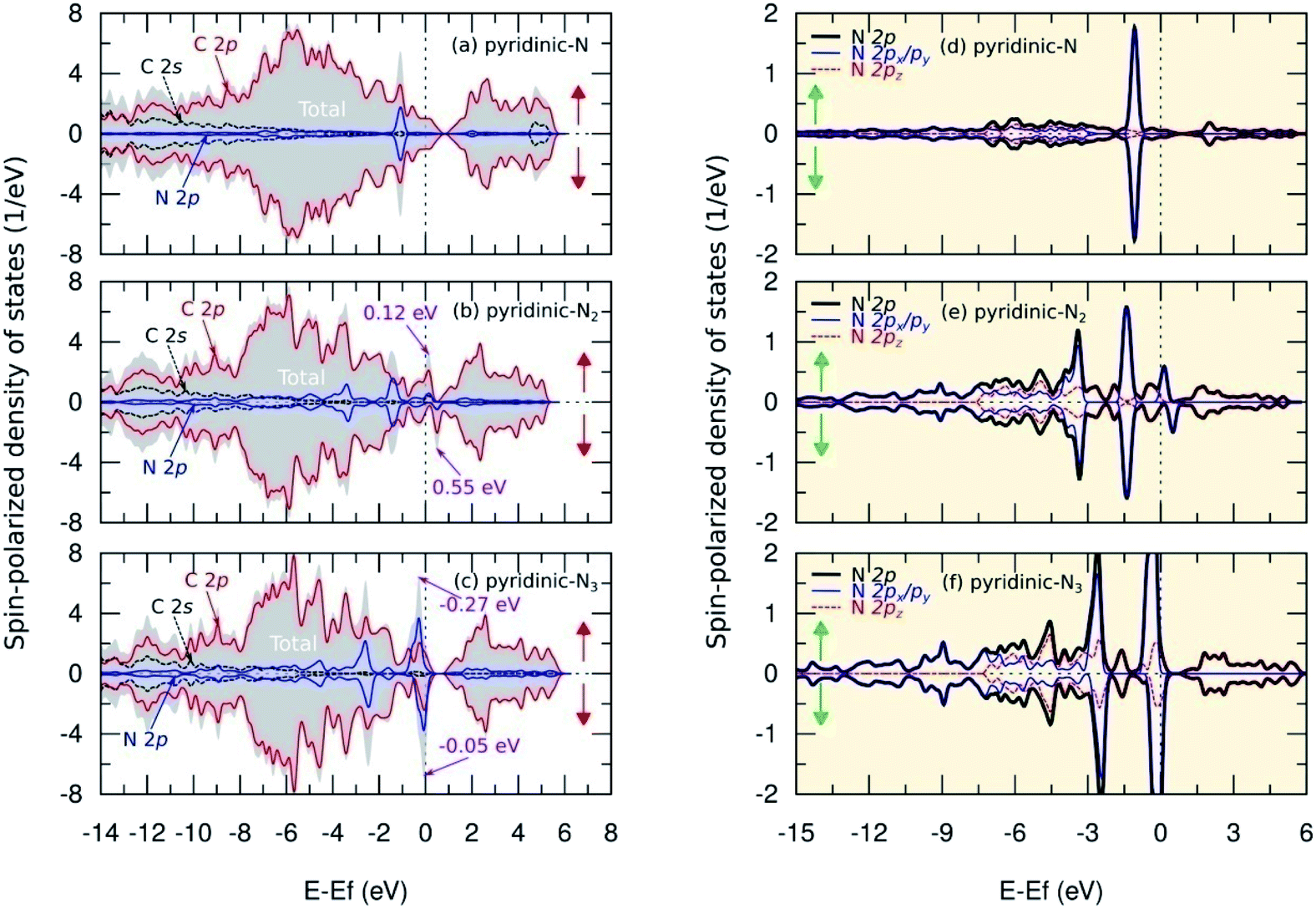 | ||
| Fig. 8 Spin-polarized density of states (SPDOS) of C 2s, C 2p, and N 2p orbitals in (a) pyridinic-N, (b) pyridinic-N2, and (c) pyridinic-N3 models. We also present SPDOS curve of sub-N 2p (px, py, pz) orbitals in (d) pyridinic-N, (e) pyridinic-N2, and (f) pyridinic-N3 models. The spin-up and spin-down states are denoted by ↑ and ↓. | ||
Fig. 8(c) shows that, in the pyridinic-N3 model, asymmetry also occurred between SPDOS of spin-up and spin-down states located at the energy levels of −0.27 eV and −0.05 eV. The SPDOS asymmetry implies a transition of paramagnetic properties with a total magnetic moment of 0.400 μB per cell. The magnetic moment of 0.050 μB per atom was centered on the three nitrogen atoms. These results were supported by the SPDOS of sub-N 2p visualization in Fig. 8(f), which shows the N 2p orbital triggered the asymmetry between the SPDOS of the spin-up and spin-down states. The increase in the magnetic moment of nitrogen atoms in this model was predicted based on the delocalized electrons in the π orbital. This prediction emerged after observing the increase in the C–N bond length of a pyridinic-N3 model (Table 1), which caused the overlap between the π orbitals to decrease and electrons likely to be unpaired. The formation of an unpaired electron increased the magnetic moment of the nitrogen atom in this model. We also compare the magnetic moment in the pyridinic configuration obtained from this study with several previous results, as shown in Table 3. For the pyridinic-N3 model, the results of this study are consistent with the results obtained by Kattel et al.45 and slightly different from the results obtained by Ma et al.26 using a local density approximation that slightly overestimates the magnetic moment calculation. These results indicate the formation of pyridinic bonds effectively modifies the magnetic properties of graphene as a candidate for future nanomagnetic materials.
4. Conclusions
We studied the effects of the number of nitrogen dopants on the electronic and magnetic properties of graphitic and pyridinic N-doped graphene. The formation of the graphitic configuration generated metallic graphene with n-type conductivity. The opening bandgap increased with the number of dopant atoms. The most significant bandgap of 0.583 eV resulted in the graphitic-N3 model. Meanwhile, the formation of a pyridinic configuration yielded metallic graphene with p-type conductivity. The increase in the number of dopants also caused the bandgap to enlarge. The most significant bandgap of 0.638 eV resulted in the pyridinic-N3 model. Furthermore, graphitic N-doped graphene remained nonmagnetic even though the number of dopant atoms increased. In contrast, pyridinic N-doped graphene is paramagnetic, and increasing the number of dopant atoms could increase the total magnetic moment in this model. The most extensive total magnetic moment occurred in the pyridinic-N3 model, which was 0.400 μB per cell. This study shows that pyridinic N-doped graphene has the potential for future nanoelectronic and nanomagnetic materials.Author contributions
E. B. Y., F. A. N., and T. W. designed and conceived the study. E. B. Y. conducted the simulation, analyzed the data and wrote the initial paper. F. A. N. and T. W. revised the paper, wrote proposal and acquired project funding. All authors confirmed the final manuscript.Conflicts of interest
There are no conflicts to declare.Acknowledgements
E. B. Y. gratefully acknowledges Program Magister-Doktor untuk Sarjana Unggul (PMDSU) Republik Indonesia which has funded this study with contract number: 201/SP2H/PMDSU/DRPM/2020.References
- A. K. Geimand and I. V. Grigorieva, Nature, 2013, 499, 419–425 CrossRef PubMed.
- K. Nagashio, Semicond. Sci. Technol., 2020, 35, 103003 CrossRef CAS.
- S. Z. Butler, S. M. Hollen, L. Cao, Y. Cui, J. A. Gupta, H. R. Gutierrez, T. F. Heinz, S. S. Hong, J. Huang, A. F. Ismach, E. Johnston-Halperin, M. Kuno, V. V. Plashnitsa, R. D. Robinson, R. S. Ruoff, S. Salahuddin, J. Shan, L. Shi○, M. G. Spencer, M. Terrones, W. Windl and J. E. Goldberger, ACS Nano, 2013, 7, 2898–2926 CrossRef CAS PubMed.
- D. A. Badurin, A. V. Tyurnina, G. L. Yu, A. Mishchenko, V. Zolyomi, S. V. Morozov, R. K. Kumar, R. V. Gorbachev, Z. R. Kudrynskyi, S. Pezzini, Z. D. Kovalyuk, U. Zeitler, K. S. Novoselov, A. Patane, L. Eaves, I. V. Grigorieva, V. I. Fal'ko, A. K. Geimand and Y. Cao, Nat. Nanotechnol., 2017, 12, 223–227 CrossRef PubMed.
- D. Sun, G. Aivazian, A. M. Jones, J. S. Ross, W. Yao, D. Cobden and X. Xu, Nat. Nanotechnol., 2012, 7, 114–118 CrossRef CAS PubMed.
- S. V. Morozov, K. S. Novoselov, M. I. Katsnelson, F. Schedin, D. C. Elias, J. A. Jaszczak and A. K. Geim, Phys. Rev. Lett., 2008, 100, 016602 CrossRef CAS PubMed.
- A. H. C. Neto, F. Guinea, N. M. R. Peres, K. S. Novoselov and A. K. Geim, Rev. Mod. Phys., 2009, 81, 109 CrossRef.
- D. G. Papageorgiou, I. A. Kinlocg and R. J. Young, Prog. Mater. Sci., 2017, 90, 75–127 CrossRef CAS.
- K. Ho, C. Huang, J. Liao, w. Zhang, L. Li, C. Lai and C. Shu, Sci. Rep., 2014, 4, 5893 CrossRef CAS PubMed.
- W. Han, R. K. Kawakami, M. Gmitra and J. Febian, Nat. Nanotechnol., 2014, 9, 794–807 CrossRef CAS PubMed.
- F. Schwierz, Nat. Nanotechnol., 2010, 5, 487–496 CrossRef CAS PubMed.
- D. Zhan, J. Yan, L. Lai, Z. Ni, L. Liu and Z. Shen, Adv. Mater., 2012, 24, 4055–4069 CrossRef CAS PubMed.
- E. Suhendi, R. Syariati, F. A. Noor, N. Kurniasih and K. Khairurrijal, Adv. Mat. Res., 2014, 974, 205–209 Search PubMed.
- P. Błoński, J. Tuček, Z. Sofer, V. Mazánek, M. Petr, M. Pumera, M. Otyepka and R. Zbořil, J. Am. Chem. Soc., 2017, 139, 3171–3180 CrossRef PubMed.
- N. U. J. Hauwali, I. Syuhada, V. E. Ligasetiawan and T. Winata, IOP Conf. Ser., Mater. Sci. Eng., 2019, 578, 012037 CrossRef.
- E. Suhendi, F. A. Noor, N. Kurniasih and K. Khairurrijal, Adv. Mat. Res., 2014, 896, 367–370 Search PubMed.
- G. Yang, D. Bao, H. Liu, D. Zhang, N. Wang and H. Li, J. Inorg. Organomet. Polym. Mater., 2017, 27, 1129–1141 CrossRef CAS.
- L. Lin, J. Li, Q. Yuan, Q. Li, J. Zhang, L. Sun, D. Rui, Z. Chen, K. Jia, M. Wang, Y. Zhang, M. H. Rummeli, N. Kang, H. Q. Xu, F. Ding, H. Peng and Z. Liu, Sci. Adv., 2019, 5, 1–9 Search PubMed.
- X. Zhou, C. Zhao, G. Wu, J. Chen and Y. Li, Appl. Surf. Sci., 2018, 459, 354–362 CrossRef CAS.
- P. Lazar, R. Mach and M. Otyepka, J. Phys. Chem. C, 2019, 123, 10695–10702 CrossRef CAS.
- D. Wei, Y. Liu, Y. Wang, H. Zhang, L. Huang and G. Yu, Nano Lett., 2009, 9, 1752–1758 CrossRef CAS PubMed.
- S. Chen, Y. Xu, C. Li, X. Xiao and Y. Chen, Sol. Energy, 2018, 174, 66–72 CrossRef CAS.
- X. Jiang, H. Shi, J. Shen, W. Han, X. Sun, J. Li and L. Wang, J. Electroanal. Chem., 2018, 823, 32–39 CrossRef CAS.
- A. Ejoz and S. Jeon, Int. J. Hydrog. Energy, 2018, 43, 5690–5702 CrossRef.
- S. Jalili and R. Varizi, Mol. Phys., 2011, 109, 687–694 CrossRef CAS.
- C. Ma, X. Shao and D. Cao, J. Mater. Chem., 2012, 22, 8911–8915 RSC.
- J. Zhang, L. Ma, M. Zhang, L. Ma and J. Zhang, Superlattice Microst, 2020, 139, 106363 CrossRef CAS.
- O. Olaniyan, R. E. Maphasha, M. J. Madito, A. A. Khaleed, E. Igumbor and N. Manyala, Carbon, 2018, 129, 207–227 CrossRef CAS.
- Z. F. Hou, X. L. Wang, T. Ikeda, K. Terakura, M. Oshima, M. Kakimoto and S. Miyata, Phys. Rev. B: Condens. Matter Mater. Phys., 2012, 85, 165439 CrossRef.
- Z. F. Hou, X. L. Wang, T. Ikeda, K. Terakura, M. Oshima and M. Kakimoto, Phys. Rev. B: Condens. Matter Mater. Phys., 2013, 87, 165401 CrossRef.
- C. Zhang, Y. Zhang, P. T. Cummings and D. Jiang, Phys. Chem. Chem. Phys., 2016, 18, 4668 RSC.
- S. N. Faisal, E. Haque, N. Noorbehesht, W. Zhang, A. T. Harris, T. L. Church and A. I. Minett, RSC Adv., 2017, 7, 17950–17958 RSC.
- C. P. Ewels and M. Glerup, J. Nanosci. Nanotechnol., 2005, 5, 1345–1363 CrossRef CAS PubMed.
- P. Giannozzil, S. Baroni, N. Bonini, M. Calandra, R. Car, C. Cavazzoni, D. Ceresoli, G. L. Chiarotti, M. Cococcioni, I. Dabo, A. D. Corso, S. d. Gironcoli, S. Fabris, G. Frestesi, R. Gebauer, U. Gerstmann, C. Gougoussis, A. Kokalj, M. Lazzeri, L. Martin-Samos, N. Marzani, F. Mauri, R. Mazzarello, S. Paolini, A. Pasquarello, L. Paulatto, C. Sbraccia, S. Scandolo, G. Sclauzero, A. P. Seitsonen, A. Smogunov, P. Umari and R. M. Wentzcovitch, J. Phys. Condens. Matter, 2009, 21, 395502 CrossRef PubMed.
- P. Giannozzi, O. Andreussi, T. Brumme, O. Bunau, M. B. Nardelli, M. Calandra, R. Car, C. Cavazzoni, D. Ceresoli and M. Cococcioni, J. Phys. Condens. Matter, 2017, 29, 465901 CrossRef CAS PubMed.
- P. E. Blochl, Phys. Rev. B, 1994, 50, 17953 CrossRef PubMed.
- J. P. Perdew, K. Burke and M. Ernzerhof, Phys. Rev. Lett., 1996, 77, 3865–3868 CrossRef CAS PubMed.
- X. Zhu, K. Liu, Z. Lu, Y. Xu, S. Qi and G. Zhang, Physica E Low Dimens. Syst. Nanostruct., 2020, 117, 113827 CrossRef CAS.
- F. Buonocore, N. Lisi and O. Pulci, J. Phys. Condens. Matter, 2019, 31, 235302 CrossRef CAS PubMed.
- C. G. Broyden, IMA J. Appl. Math., 1970, 6, 76–90 CrossRef.
- R. Fletcher, Comput, 1970, 13, 317–322 Search PubMed.
- D. Goldfarb, Math. Comput., 1970, 24, 23–26 CrossRef.
- D. F. Shanno, Math. Comput., 1970, 24, 647–656 CrossRef.
- X. S. Dai, T. Shen and H. C. Liu, Mater. Res. Express, 2019, 6, 085635 CrossRef CAS.
- S. Kattel, P. Atanassov and B. Kiefer, J. Phys. Chem. C, 2012, 116, 8161–8166 CrossRef CAS.
- E. Finazzi, C. D. Valentin, A. Selloni and G. Pacchioni, J. Phys. Chem. C, 2007, 111, 9275–9282 CrossRef CAS.
- K. Yong, Y. Dai, B. Huang and S. Han, J. Phys. Chem. B, 2006, 110, 24011–24014 CrossRef PubMed.
- E. Lee, H. C. Lee, S. B. Jo, H. Lee, N. S. Lee, C. G. Park, S. K. Lee, H. H. Kim, H. Bong and K. Cho, Adv. Funct. Mater., 2016, 26, 562–568 CrossRef CAS.
- Y. Wang, W. Wang, S. Zhu, G. Yang, Z. Zhang and P. Li, RSC Adv., 2019, 9, 11939–11950 RSC.
- P. Rani and V. K. Jindalt, RSC Adv., 2013, 3, 802–812 RSC.
- Y. Ma, P. O. Lehtinen and R. M. Nieminen, New J. Phys., 2004, 6, 68–81 CrossRef.
- M. Wu, C. Cao and J. Z. Jiang, Nanotechnology, 2010, 21, 505202 CrossRef CAS PubMed.
- M. Ghadiry, R. Ismail, B. Naraghi, S. T. Abed, D. Kavosi and F. Fatovatikhah, Semicond. Sci. Technol., 2015, 30, 045012 CrossRef.
- H. Wang, H. Wang, Y. Chen, Y. Liu, J. Zhao, Q. Chai and X. Wang, Appl. Surf. Sci., 2013, 273, 302–309 CrossRef CAS.
- A. Bostwick, J. McChesney, T. Ohta, E. Rotenberg, T. Seyller and K. Horn, Prog. Surf. Sci., 2009, 84, 380–413 CrossRef CAS.
- D. Usachov, O. Vilkov, A. Grüneis, D. Haberer, A. Fedorov, V. K. Adamchuk, A. B. Preobrajenski, P. Dudin, A. Barinov, M. Oehzelt, C. Laubschat and D. V. Vyalikh, Nano Lett., 2011, 11, 5401–5407 CrossRef CAS PubMed.
- M. Ali, X. Pi, Y. Liu and D. Yang, AIP Adv, 2017, 7, 045308 CrossRef.
- J. Robertson and C. A. Davis, Diam. Relat. Mater., 1995, 4, 441–444 CrossRef CAS.
- A. C. F. Serraon, J. A. D. D. Rosario, P. A. Chuang, M. N. Chong, Y. Morikawa, A. A. B. Padama and J. D. Ocon, RSC Adv., 2021, 11, 6268–6283 RSC.
- M. Rafique, Y. Shuai, H. Tana and M. Hassana, RSC Adv., 2017, 7, 16360–16370 RSC.
| This journal is © The Royal Society of Chemistry 2021 |