
 Open Access Article
 This Open Access Article is licensed under a Creative Commons Attribution-Non Commercial 3.0 Unported Licence
Engineering tunability through electro-optic effects to manifest a multifunctional metadevice†
Taimoor Naeem,
Hafiz Saad Khaliq,
Muhammad Zubair *,
Tauseef Tauqeer* and
Muhammad Qasim Mehmood*
*,
Tauseef Tauqeer* and
Muhammad Qasim Mehmood*
NanoTech Lab, Department of Electrical Engineering, Information Technology University (ITU) of the Punjab, Ferozepur Road, Lahore 54600, Pakistan. E-mail: tauseef.tauqeer@itu.edu.pk; qasim.mehmood@itu.edu.pk; muhammad.zubair@itu.edu.pk
First published on 8th April 2021
Abstract
Ultrafast modulation of the refractive index exhibits either linear or nonlinear electro-optic (EO) effect, which is extensively utilized in tunable photonic circuits. Silicon, a mature material for on-chip devices, lacks a strong electro-optic (EO) Pockels effect. Utilization of the Pockels effect alters the intrinsic property (refractive index) of the material that manifests tunability and offers expanded functionalities. Driven by the limited space constraints in data storage, sensing, and imaging applications, we propose an electrically tunable meta-device whose resonance wavelength and focal length can be tuned by varying applied electric fields in the visible range. The fundamental unit of a metalens is the barium titanate (BTO) diffractive optical element placed on indium titanium oxide (which serves as an electrode) with SiO2 as the substrate. The metalens' tunability is characterized by point spread function (PSF), full-width half-maximum (FWHM), and imaging bandwidth that demonstrates the tuning of resonance wavelength and focal length. Moreover, polarization-insensitive meta-holograms are realized at a wavelength of 633 nm without utilizing propagation and Pancharatnam–Berry (PB) phase. The proposed study can find exciting applications in machine vision, broadband microscopy, and spectroscopy.
Introduction
Flat surfaces offer arbitrary full-wave manipulation and have been studied extensively in recent years due to their significant breakthroughs in various fields such as optical activity,1–3 holography,4–6 and optical imaging.7–9 Planar optical structures, specifically metalenses,10,11 have attained tremendous interest across the research community and developed rapidly in context of their functionalities and efficiencies. Novel metasurface-based lenses are ubiquitous for biomedical applications,12 such as endoscopy and wearable medical devices.13 These are replacing conventional bulky optical lenses such as Fresnel micro-lenses and micro-grating, which have limited imaging quality, high cost, inadequate phase coverage, and integration difficulties. The noteworthy advancements in the development of metalenses are the wide field-of-view,14,15 high aspect ratio dielectric,16 achromatic,17–20 and tunable metalens.21Tunable lenses manipulate the amplitude, phase, and polarization dynamically with the help of external stimuli. Tunability is generally introduced by any physical mechanism that forces a change in the material's intrinsic property or geometrical configuration of the diffractive optical element. Among various methods to introduce external stimuli, such as chemical activation22 and mechanical reconfiguration,23,24 an electro-optic (EO) method is in the limelight due to its benefits of compatibility, low power consumption, and fast switching. The negative birefringence primarily drives tunability due to the applied electric field, which changes the refractive index along two optical axes, i.e., ordinary and extraordinary axes. The variation of the refractive index under the electric field is linear to a certain limit known as the Pockels effect.25 It starts varying proportionally to the square of the electric field, which is called as Kerr effect.26 These effects may be exploited to have unique properties that overcome the limitations of conventional silicon-based devices, such as high operational velocity and low driving voltages.
Numerous investigations of dynamic optical responses have been conducted with EO materials such as graphene,27,28 heavily doped semiconductors,29–31 and conducting oxides.32–34 Among EO materials, lithium niobate (LiNbO3 or LN) is widely used and has a reasonable Pockel's coefficient around 30 pm V−1.35 However, its integration is challenging with silicon-based devices. On the other hand, BTO has a Pockels coefficient around 1300 pm V−1, which is 30 times higher than LiNbO3.36 Besides its low driving voltages and its ability to be grown epitaxially on the silicon substrate, it has emerged as a strong successor for EO applications.37 For a strong Pockels effect, barium titanate (BTO) appears to be an exceptional candidate for its compatibility with oxide substrates. Its usage in thin-films enhances its importance for on-chip based devices.38,39 Additionally, it exhibits the largest Pockels coefficients compared to their counterparts, increasing their tunability to extended ranges.40 Furthermore, thermal and chemical stability is proven by the realization of BTO in silicon waveguides.41
Tunability is indispensable for an ideal meta-device that realizes numerous electromagnetic responses, which not only utilizes the limited space efficiently but also integrates diverse functionalities. The possible approaches for applying voltages to introduce tunability is categorized into three schemes. The first one is to employ a single voltage source to the whole metasurface where every element of the metasurface has the same potential. The second one is to connect all the elements in rows or columns such that applying voltage to individual row leads to the same potential in every element of a row or column. The last one is to apply voltages to all the individual elements of metasurface, which is more robust but practically not realizable.
In this paper, we employed all the aforementioned schemes to the designed metasurface and demonstrated different phenomena using each scheme that offers a multi-functional platform for imaging and sensing applications. Initially, a tunable metalens is proposed, which works on the principle of EO effect and offers spectral multiplexing. A single BTO-based metalens is designed, which shifts the resonance to different wavelengths (488 nm, 532 nm, 633 nm) in the visible range under various biased voltages (−8.9 V, −16.7 V, −33.6 V, respectively). Under this scheme, the biased voltage is applied to the whole metasurface with a single voltage source, thus providing a spectral multiplexing platform. In the second scheme, each row of the metasurface is bus-connected electrically, which offers a step-zoom metalens by changing each row's voltage. The main benefit of this scheme is the fabrication flexibility since the phase of each row is governed by the voltage source, which does not need structural parameter accuracy in the fabrication process. The different focal lengths through a single metalens can be realized by applying required voltages to each pixel (row). The third scheme in which each meta-atom is connected with different voltage sources to alter the phase demonstrates polarization-insensitive holography. Previously, to achieve these phenomena, the entire metasurface needed to be changed if metasurface resonance tuning, dynamic focusing (step-zoom), or holography is required.
Background and design
To achieve the desired phase profile with high amplitude, a two-dimensional array of BTO meta-atoms are placed at the substrate as shown in Fig. 1(a) and (b). Significant birefringence should be introduced for attaining desired phase control along with photon spin reversal. To achieve this effect, we employed optimized nanobars that behave as a half-wave plate, yielding a phase shift with the cross-polarized component. The attained phase shift increases linearly (from 0–2π), as the orientation angle between the fast axis and x-axis is rotated (from 0–π). To accomplish the phase coverage (0–2π), phase modulation realized by Pancharatnam–Berry (PB) is implemented42 by varying only the rotation of nanobar. | ||
| Fig. 1 (a) Demonstration of tunable metalens focusing the light of wavelengths of 488 nm, 532 nm and 633 nm by varying voltages to V1, V2 and V3, respectively. (b) Underlying mechanism of the step zoom metalens for different focal points at a wavelength of 633 nm. (c) Perspective view of the designed meta-atom with parameters (P = 350 nm) height (H = 500 nm), length (L = 250 nm) width (W = 65 nm) that works in the visible range (d) single tunable metasurface displaying hologram at two different wavelengths by merely varying voltages. | ||
The wavefront of the incident light can be engineered by a high refractive index meta-atom since it has a localized ability to change the phase. Arranging these meta-atoms in an array following the hyperbolic phase profile constructs the metasurface-based lens. The underlying phenomenon of the tunable lens of focusing on different wavelengths and step zoom under external stimuli (electric field) is depicted in Fig. 1(a) and (b), respectively. The BTO-based meta-atom is supported by ITO, which serves as an electrode to deliver voltage to regulate refractive index, and is placed on the SiO2. The structural parameters such as periodicity (P), length (L), and width (W) are optimized to achieve the maximum cross-polarized transmission coefficient as shown in Fig. 1(c). Among the designed parameters, the period of meta-atom is taken as 350 nm, which has a limit of Nyquist criterion, i.e., the maximum period should follow p < λ/2NA, where λ is the wavelength and NA is the numerical aperture.
Numerical simulations have been performed for transmission efficiency by the sweeping length from 170 nm to 300 nm and width from 50 nm to 120 nm of the meta-atom. We employed a finite difference time domain (FDTD) algorithm to optimize the meta-atom at a working wavelength of 550 nm by taking a perfectly-matched layer along the propagation axis, i.e., z-axis, and periodic boundary conditions in x and y directions. Fig. 2(a) shows that BTO provides high transmission efficiency across different lengths and widths. The co-polarized component for the BTO nanobar is shown in Fig. 2(b), which is minimum at the desired wavelength thus working as optimized halfwave plate. The optimized L and W for the meta-atom is 250 nm and 65 nm, respectively, where the cross-polarized component is minimum, and the cross-polarized component is maximum. The acquired phase of the meta-atom with geometrical parameters is L = 250 nm and W = 65 nm is shown in Fig. 2(c).
 | ||
| Fig. 2 (a) Cross-polarized and (b) co-polarized component of tunable BTO based optical diffractive element (c) phase of the tunable diffractive optical element at different rotations (d) change in refractive index across different voltages. | ||
For designing an electrically tunable meta device, we start designing a metalens at a wavelength of 550 nm, whose phase profile is compensated spatially by each meta-atom. The desired spatial phase for this particular scheme is achieved by manipulating the geometric phase (Pancharatnam–Berry (PB) phase) of the meta-atom. The equation for a lens phase profile is expressed by
 | (1) |
The designed metasurface-based lens modulates the incident planar wavefront into the spherical to focus light on the focal plane. Commonly, modulators encode optical signals by changing the phase and intensity of the light, while the EO effect provides a platform to control phase by varying refractive index. This control over the refractive index allows us to tune the designed meta-device to shift wavelength resonances under different electric fields.
Results and discussion
The tunability of refractive index is primarily driven by Pockels effect, which exists only in materials that possess non-centrosymmetric crystal structures. Semiconductors, such as silicon, possess low optical loss and exhibit a centrosymmetric structure, lacking strong Pockels effect. The non-centrosymmetric crystal structure of BTO provides high Pockels coefficient, thus offering refractive index tunability to extended ranges with low power consumption. The dynamic optical response of a material is determined by change in refractive index upon applying voltage, which eventually becomes the merit for power consumption. The parameter that governs the dynamic response or tunability is the Pockels coefficient of a material. The detailed mathematical derivation to extract the Pockels coefficient of a given material is presented in ESI Note 1.† In Table 1, different materials including heavily doped semiconductors and conducting oxides are tabulated along with their corresponding Pockels coefficient denoted by “r” and measurement conditions. It is evident from Table 1 that among other EO materials BTO has a very high Pockels coefficient, which makes it an exceptional choice.| Material | r (pm V−1) | Wavelength (nm) | Temperature (°C) | Refractive index (n) | Reference |
|---|---|---|---|---|---|
| Bi12SiO20 | 5 | 633 | 22–502 | 2.54 | 43 |
| Bi12TiO20 | 5.5 | 633 | — | 2.578 | 44 |
| LiTaO3 | 30.5 | 632.8 | 0–500 | 2.45 | 45 |
| LiNbO3 | 33 | 633 | 0–500 | 2.286 | 46 |
| Bi12GeO20 | 3.22 | 666 | 20 | 2.54 | 47 |
| Ba0.4Sr0.6TiO3 | 350 | 510 | 20–50 | 2.36 | 48 |
| KNbO3 | 450 | 633 | 20–180 | 2.329 | 49 |
| BaTiO3 | 1300 | 546 | 25 | 2.45 | 50 |
The utilization of the EO effect for controlling the refractive index by varying various bias voltages is given by
| δnl = −0.5n3rlkEk | (2) |
The performance of the tunable metalens is characterized in terms of their focal spot profiles. Benefitting from the EO effect, the designed tunable metalens can operate at three different wavelengths (488 nm, 532 nm, 633 nm) in the visible range under different applied voltages (−8.9 V, −16.6 V, −33.7 V, respectively). Three simulations have been performed at each wavelength for the focal spot profiles under different voltages to analyze the metalens performance, as shown in Fig. 3. The focal profiles are computed by normalizing with the highest electric field amplitude at each wavelength. Fig. 3(a)–(c) demonstrate the lens focal spot in the xy plane at the wavelength of 488 nm, 532 nm and 633 nm by applying −8.9 volts (n = 2.51), −16.6 volts (n = 2.69), and 33.7 volts (n = 3), respectively. Fig. 3(d)–(f) depict focal points in the xz plane at the wavelength of 488 nm, 532 nm and 633 nm by applying −8.9 volts (n = 2.51), −16.6 volts (n = 2.69), and 33.7 volts (n = 3), respectively, which demonstrates the tunability of PSF for the designed lens.
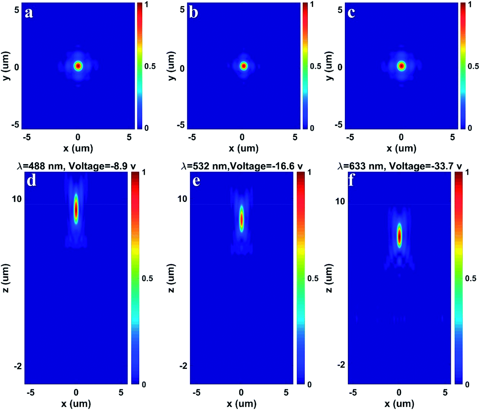 | ||
| Fig. 3 Simulated point spread function (PSF) for tunable metalens with different applied voltages in the xz plane with normal incident light. PSF or focal spot in the xy plane for an incident wavelength of (a) 488 nm, (b) 532 nm and (c) 633 nm with applied voltages of −8.9, −16.6 and 33.7, respectively. PSF or focal spot in the xz plane for an incident wavelength of (d) 488 nm, (e) 532 nm and (f) 633 nm with applied voltages of −8.9, −16.6 and 33.7, respectively. | ||
Another figure of merit that describes the limit for maximum resolution is full-width at half-maximum (FWHM), which is defined as the wavelength region where transmittance remains half of the maximum value. Fig. 4(a)–(c) show FWHM at the wavelength of 488 nm, 532 nm, and 633 nm, which illustrates that FWHM for these wavelengths is limited to half of the working wavelength. Fig. 4(d) illustrates FWHM at a wavelength of 488 nm, 532 nm, and 633 nm under all the possible applied voltages of −8.9 V, −16.6 V, and −33.7 V. The spectral multiplexing of the metalens is demonstrated by varying only the bias voltage, without manipulating the geometry of the metasurface.
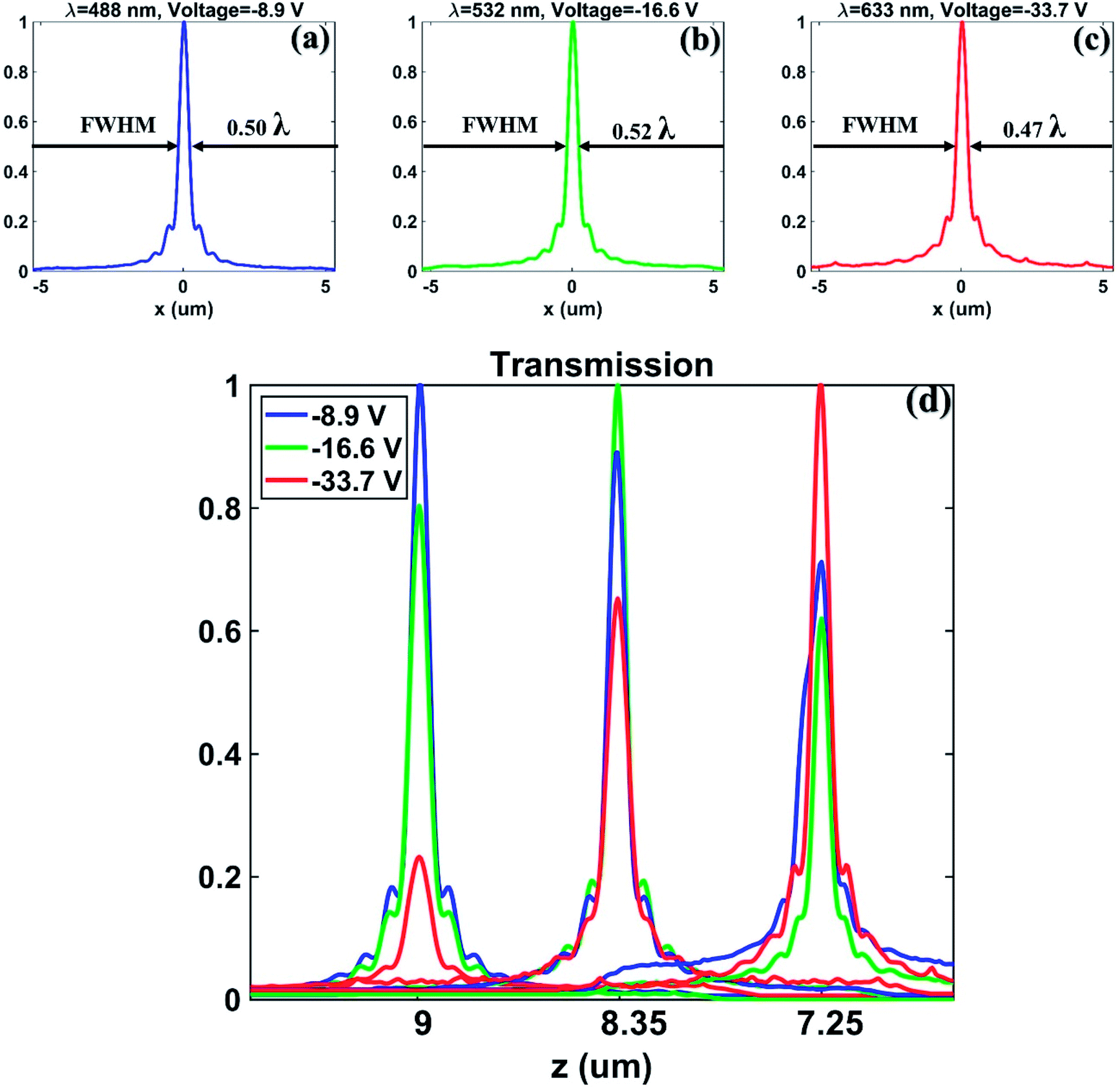 | ||
| Fig. 4 Simulated full-width at half maximum (FWHM) for the designed tunable metalens with varying applied voltages. FWHM for the incident wavelength of (a) 488 nm with an applied voltage of −8.9 V (b) 532 nm with an applied voltage of −16.6 V. (c) 633 nm with an applied voltage of −33.7 V. (d) FWHM for each incident wavelength of 488 nm, 532 nm, and 633 nm under each applied voltages of −8.9, −16.6, and 33.7, respectively. | ||
To further corroborate the tunability, we demonstrated a “star” shaped hologram designed at 550 nm wavelength, as shown in Fig. 1(d). The phase map for the “star” shaped hologram is acquired with an adaptive Gerchberg–Saxton (GS) algorithm, which forms the image of non-existing objects in the far-field. This phase map is translated at the metasurface, where each pixel phase is realized through the rotation of the meta-atom by utilizing the PB phase. This single metasurface is illuminated with light of wavelength of 488 nm and observed with applied voltages of −8.9 V and −33.7 V. From Fig. 5(a) and (b), it can be observed that the metasurface demonstrates the star-shaped hologram at −8.9 V, and for −33.7 V the intensity of the hologram is diminished. For the incident wavelength of 633 nm, the hologram is unclear [Fig. 5(c)] by applying −8.9 V, while at −33.7 V, the hologram is clearly displayed at the focal plane as shown in Fig. 5(d). It clearly emphasizes that a single metasurface working wavelength can be controlled only by varying the applied electric field or voltage of the metasurface.
 | ||
| Fig. 5 Simulated tunable holograms with varying applied voltages in the xy plane with normal incident light. The metasurface is designed as a 100 × 100 array at a wavelength of 550 nm with a focal plane at 28 μm. A star-shaped hologram is illustrated at an incident wavelength of 488 nm at applied voltages of (a) −8.9 V and (b) −33.7 V. Star hologram demonstrated for the incident wavelength of 633 nm at an applied voltage of (c) −8.9 V and (d) −33.7 V. | ||
After controlling the spectral tunability of our metasurface, we designed a tunable zoom metalens at the wavelengths of 488 nm, 532 nm, and 633 nm, respectively, because practically realizable meta-devices do not allow one to vary the voltages of individual elements. To address this, we connected unit elements electrically in one direction, resulting in equipotential rows. Each row is considered a pixel that can be controlled by applying separate voltage to acquire the required phase. The spatial phase profile for dynamic zooming at different focusing is attained by a one-dimensional lens equation assuming the rows are bus-connected (ESI Note 2†). The spatial phase profile for focusing at 25 μm and 40 μm for a wavelength of 488 nm (Fig. 6(g and h)), 532 nm (Fig. 6(i and j)), and 633 nm (Fig. 6(k and l)) is illustrated. The corresponding voltage distribution to attain the required spatial phase profile for focusing at 25 μm and 40 μm for a wavelength of 488 nm, 532 nm, and 633 nm is depicted in Fig. 6(a, b), (c, d) and (e, f), respectively. By applying the required voltages to each pixel, the far-field pattern of the transmitted electric field of tunable focusing metasurface is illustrated in the xz plane. The dynamic zooming with focusing from 25 μm to 40 μm with a 5 μm step is illustrated in ESI Note 2.† The electric field transmission is demonstrated with focusing at 25 μm and 40 μm at the wavelength of 488 nm, 532 nm, and 633 nm as depicted in Fig. 6(m, n), (o, p) and (q, r), respectively. The focusing of the tunable metasurface is realized at f = 25 μm and f = 40 μm upon applying acquired bias voltages to the metasurface pixels.
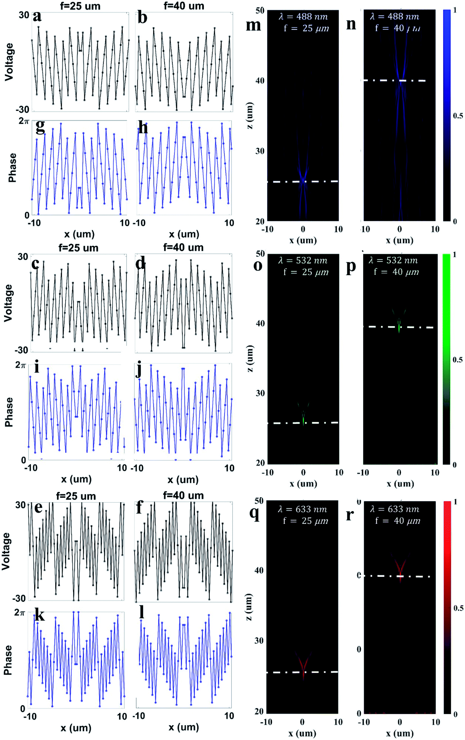 | ||
| Fig. 6 Demonstration of tunable focusing metalens. Voltage distribution for focusing at 25 μm and 40 μm for the wavelength of (a and b) 488 nm, (c and d) 532 nm, and (e and f) 633 nm, respectively. The corresponding phase distribution at simulated voltages for focusing at 25 μm and 40 μm for the wavelength of (g and h) 488 nm, (i and j) 532 nm, and (k and l) 633 nm, respectively. Full-wave simulation of |E|2 for focusing at 25 μm and 40 μm at the wavelength of (m and n) 488 nm, (o and p) 532 nm, and (q and r) 633 nm, respectively. | ||
Finally, the approach in which each individual element is provided by a separate voltage is illustrated. To validate phase control by biased voltages, we implemented a “star” shaped hologram with different point sources where each point source exhibits a specific phase. The 360° phase map of the “star” shaped hologram is encoded into eight different voltage levels, which provide a phase difference of 45°. The metasurface size is 35 × 35 μm2, which forms a phase matrix of 100 × 100 elements with a pixel of 350 nm by using the finite difference time domain (FDTD) algorithm. The perfect matched layer boundary condition is applied and a monitor is placed at 28 μm to extract the electric fields at the far-field. Fig. 7 demonstrates the designed metasurface subjected to various polarizations depicting optical outputs. The holographic image of equal intensity is obtained under (Fig. 7(a)) linear horizontal polarized (LHP), (Fig. 7(b)) linear vertical polarized (LVP), (Fig. 7(c)) LCP, and (Fig. 7(d)) RCP, respectively, demonstrating polarization-insensitive holography.
 | ||
| Fig. 7 Polarization insensitive meta-hologram is demonstrated with the interference of point sources of the metasurface. Reconstruction of “star” shaped holographic image under (a) LHP (b) LVP (c) LCP (d) RCP. | ||
Conclusion
By using the electro-optic effect, the intrinsic property (refractive index) of the material is tuned to achieve control on the wavelength resonance of the metalens. The high Pockels coefficient of BTO allows us to effectively control the refractive index, which eventually leads to the tunability of the device. The designed meta-device serves for the applications where spectral multiplexing is required in the visible range. Furthermore, it is analyzed theoretically to control the refractive index variation under applied electric fields characterized by the PSF, FWHM, and imaging bandwidth. The diffraction-limited imaging is achieved at the wavelengths of 488 nm, 532 nm, and 633 nm of the visible regime. Moreover, a step-zoom metalens is designed whose focal length can be altered by varying applied voltages. These tunable meta-devices find numerous applications in the imaging field, such as microscopy, machine vision, endoscopy, and augmented reality.Conflicts of interest
There are no conflicts to declare.References
- S. Chen, B. Reineke, G. Li, T. Zentgraf and S. Zhang, Nano Lett., 2019, 19, 6278–6283 CrossRef CAS PubMed.
- E. Plum, V. A. Fedotov and N. I. Zheludev, Appl. Phys. Lett., 2016, 108, 141905 CrossRef.
- O. V. Kotov and Y. E. Lozovik, Phys. Rev. B, 2017, 96, 235403 CrossRef.
- T. Naeem, A. S. Rana, M. Zubair, T. Tauqeer and M. Q. Mehmood, Opt. Mater. Express, 2020, 10, 3342–3352 CrossRef CAS.
- H. S. Khaliq, K. Riaz, M. Zubair, M. A. Ansari, M. R. Akram, T. Naeem, J. Zhang, W. Zhu, D. Zhang, X. Wang and M. Q. Mehmood, Proc. SPIE 11344, Metamaterials, 2020, XII, 113441N Search PubMed.
- H. S. Khaliq, M. R. Akram, K. Riaz, M. A. Ansari, J. Akbar, J. Zhang, W. Zhu, D. Zhang, X. Wang, M. Zubair and M. Q. Mehmood, Opt. Express, 2021, 29, 3230–3242 CrossRef CAS PubMed.
- W. Wan, J. Gao and X. Yang, Adv. Opt. Mater., 2017, 5, 1700541 CrossRef.
- F. Zhang, M. Pu, X. Li, P. Gao, X. Ma, J. Luo, H. Yu and X. Luo, Adv. Funct. Mater., 2017, 27, 1704295 CrossRef.
- N. Mahmood, H. Jeong, I. Kim, M. Q. Mehmood, M. Zubair, A. Akbar, M. Saleem, M. S. Anwar, F. A. Tahir and J. Rho, Nanoscale, 2019, 11, 20571–20578 RSC.
- H. S. Khaliq, K. Riaz, M. Zubair, M. A. Ansari, T. Naeem and M. Q. Mehmood, Proc. SPIE 11461, Active Photonic Platforms, 2020, XII, 114612P Search PubMed.
- M. Khorasaninejad, W. T. Chen, A. Y. Zhu, J. Oh, R. C. Devlin, D. Rousso and F. Capasso, Nano Lett., 2016, 16(7), 4595–4600 CrossRef CAS PubMed.
- D. Sun, Y. Yang, S. Liu, Y. Li, M. Luo, X. Qi and Z. Ma, Biomed. Opt. Express, 2020, 11, 4408–4418 CrossRef CAS PubMed.
- S. Zhang, C. L. Wong, S. Zeng, R. Bi, K. Tai, K. Dholakia and M. Olivo, Nanophotonics, 2021, 10, 259–293 CAS.
- J. Engelberg, C. Zhou, N. Mazurski, J. Bar-David, A. Kristensen and U. Levy, Nanophotonics, 2013, 7, 739–745 Search PubMed.
- G. Zheng, R. Horstmeyer and C. Yang, Nat. Photonics, 2013, 7, 739–745 CrossRef CAS PubMed.
- B. Wu, A. Kumar and S. Pamarthy, J. Appl. Phys., 2010, 108, 9 Search PubMed.
- F. Aieta, M. A. Kats, P. Genevet and F. Capasso, Science, 2015, 347, 1342–1345 CrossRef CAS PubMed.
- S. Shrestha, A. C. Overvig, M. Lu, A. Stein and N. Yu, Light: Sci. Appl., 2018, 7, 1–11 CrossRef CAS PubMed.
- M. Khorasaninejad, F. Aieta, P. Kanhaiya, M. A. Kats, P. Genevet, D. Rousso and F. Capasso, Nano Lett., 2015, 15, 5358–5362 CrossRef CAS PubMed.
- S. Wang, P. C. Wu, V. C. Su, Y. C. Lai, M. K. Chen, H. Y. Kuo, B. H. Chen, Y. H. Chen, T. T. Huang, J. H. Wang, R. M. Lin, C. H. Kuan, T. Li, Z. Wang, S. Zhu and D. P. Tsai, Nat. Nanotechnol., 2018, 13, 227–232 CrossRef CAS PubMed.
- R. Fu, Z. Li, G. Zheng, M. Chen, Y. Yang, J. Tao, L. Wu and Q. Deng, Opt. Express, 2018, 13, 227–232 Search PubMed.
- P. Yu, J. Li, S. Zhang, Z. Jin, G. Schütz, C. W. Qiu, M. Hirscher and N. Liu, Nano Lett., 2018, 18, 4584–4589 CrossRef CAS PubMed.
- J. Valente, J. Y. Ou, E. Plum, I. J. Youngs and N. I. Zheludev, Nat. Commun., 2015, 6, 1–7 Search PubMed.
- N. I. Zheludev and E. Plum, Nat. Nanotechnol., 2016, 11, 16 CrossRef CAS PubMed.
- K. J. Kormondy, Y. Popoff, M. Sousa, F. Eltes, D. Caimi, M. D. Rossell, M. Fiebig, P. Hoffmann, C. Marchiori, M. Reinke, M. Trassin, A. A. Demkov, J. Fompeyrine and S. Abel, Nanotechnology, 2017, 28, 075706 CrossRef PubMed.
- E. Freysz and J. Degert, Nat. Photonics, 2010, 4, 131–132 CrossRef CAS.
- Y. Yao, M. A. Kats, P. Genevet, N. Yu, Y. Song, J. Kong and F. Capasso, Nano Lett., 2013, 13, 1257–1264 CrossRef CAS PubMed.
- Q. Bao, H. Zhang, B. Wang, Z. Ni, C. H. Y. X. Lim, Y. Wang, D. Y. Tang and K. P. Loh, Nat. Photonics, 2011, 5, 411–415 CrossRef CAS.
- M. R. Shcherbakov, S. Liu, V. V. Zubyuk, A. Vaskin, P. P. Vabishchevich, G. Keeler, T. Pertsch, T. V. Dolgova, I. Staude, I. Brener and A. A. Fedyanin, Nat. Commun., 2017, 8, 1–6 CrossRef CAS PubMed.
- P. P. Iyer, M. Pendharkar and J. A. Schuller, Adv. Opt. Mater., 2016, 4, 1582–1588 CrossRef CAS.
- X. Su, C. Ouyang, N. Xu, W. Cao, X. Wei, G. Song, J. Gu, Z. Tian, J. F. O'Hara, J. Han and W. Zhang, Opt. Express, 2015, 23, 27152–27158 CrossRef CAS PubMed.
- G. V. Naik, J. Kim and A. Boltasseva, Opt. Mater. Express, 2011, 1, 1090–1099 CrossRef CAS.
- A. Boltasseva and H. A. Atwater, Science, 2011, 331, 290–291 CrossRef CAS PubMed.
- J. Park, J. H. Kang, X. Liu and M. L. Brongersma, Sci. Rep., 2015, 5, 1–9 CAS.
- E. L. Wooten, K. M. Kissa, A. Yi-Yan, E. J. Murphy, D. A. Lafaw, P. F. Hallemeier, D. Maack, D. V. Attanasio, D. J. Fritz, G. J. McBrien and D. E. Bossi, IEEE J. Sel. Top. Quantum Electron., 2000, 6, 69–82 CAS.
- M. Li and H. X. Tang, Nat. Mater., 2019, 18, 9–11 CrossRef CAS PubMed.
- S. Abel, F. Eltes, J. E. Ortmann, A. Messner, P. Castera, T. Wagner, D. Urbonas, A. Rosa, A. M. Gutierrez, D. Tulli, P. Ma, B. Baeuerle, A. Josten, W. Heni, D. Caimi, L. Czornomaz, A. A. Demkov, J. Leuthold, P. Sanchis and J. Fompeyrine, Nat. Mater., 2019, 18, 42–47 CrossRef CAS.
- P. Girouard, P. Chen, Y. K. Jeong, Z. Liu, S. T. Ho and B. W. Wessels, IEEE J. Quantum Electron., 2017, 53, 1–10 Search PubMed.
- A. Petraru, J. Schubert, M. Schmid, O. Trithaveesak and C. Buchal, Opt. Lett., 2003, 28, 2527–2529 CrossRef CAS.
- S. Abel, T. Stöferle, C. Marchiori, C. Rossel, M. D. Rossell, R. Erni, D. Caimi, M. Sousa, A. Chelnokov, B. J. Offrein and J. Fompeyrine, Nat. Commun., 2013, 4, 1–6 Search PubMed.
- W. Cai, C. Fu, J. Gao, Q. Guo, X. Deng and C. Zhang, Phys. Rev. B: Condens. Matter Mater. Phys., 2011, 406, 3583–3587 CrossRef CAS.
- M. Khorasaninejad and K. B. Crozier, Nat. Commun., 2011, 406, 3583–3587 Search PubMed.
- H. Xu, Y. Zhang, H. Zhang, H. Yu, Z. Pan, Y. Wang, S. Sun, J. Wang and R. I. Boughton, Opt. Commun., 2012, 285, 3961–3966 CrossRef CAS.
- S. Unser, I. Bruzas, J. He and L. Sagle, Sensors, 2015, 17, 6532–6539 Search PubMed.
- O. B. Jensen, P. E. Andersen, B. Sumpf, K.-H. Hasler, G. Erbert and P. M. Petersen, Opt. Express, 2009, 17, 6532–6539 CrossRef CAS.
- S. Mamoun, A. E. Merad and L. Guilbert, Comput. Mater. Sci., 2013, 79, 125–131 CrossRef CAS.
- K. Vedam and P. Hennessey, J. Opt. Soc. Am., 1975, 65, 442–445 CrossRef CAS.
- B. W. Wessels, Annu. Rev. Mater. Res., 2007, 37, 659–679 CrossRef CAS.
- G. Ghosh, Appl. Phys. Lett., 1994, 65, 3311–3313 CrossRef CAS.
- M. Zgonik, P. Bernasconi, M. Duelli, R. Schlesser, P. Günter, M. H. Garrett, D. Rytz, Y. Zhu and X. Wu, Phys. Rev. B: Condens. Matter Mater. Phys., 1994, 50, 5941 CrossRef CAS PubMed.
Footnote |
| † Electronic supplementary information (ESI) available. See DOI: 10.1039/d1ra00901j |
| This journal is © The Royal Society of Chemistry 2021 |